 | –≠–ª–µ–∫—Ç—Ä–æ–Ω–Ω—ã–π –∫–æ–º–ø–æ–Ω–µ–Ω—Ç: HT9200A | –°–∫–∞—á–∞—Ç—å:  PDF PDF  ZIP ZIP |

HT9200A/B
DTMF Generators
Selection Table
Block Diagram
Features
∑
Operating voltage: 2.0V~5.5V
∑
Serial mode for the HT9200A
∑
Serial/parallel mode for the HT9200B
∑
Low standby current
∑
Low total harmonic distortion
∑
3.58MHz crystal or ceramic resonator
General Description
The HT9200A/B tone generators are designed
for
µ
C interfaces. They can be instructed by a
µ
C to generate 16 dual tones and 8 single tones
from the DTMF pin. The HT9200A provides a
serial mode whereas the HT9200B contains a
selectable serial/parallel mode interface for
various applications such as security systems,
home automation, remote control through tele-
phone lines, communication systems, etc.
1
21st Aug '98

Pin Assignment
Pad Assignment
Pad Coordinates
Unit:
µ
m
Pad
No.
X
Y
Pad
No.
X
Y
1
≠553.30
430.40
8
553.30
≠523.50
2
≠553.30 ≠133.50
9
553.30
≠190.30
3
≠553.30 ≠328.50
10
553.30
4.70
4
≠553.30 ≠523.50
11
553.30
340.30
5
≠220.10 ≠523.50
12
374.90
523.50
6
≠25.10
≠523.50
13
≠279.30
523.50
7
308.10
≠523.50
Chip size: 1460
◊
1470 (
µ
m)
2
* The IC substrate should be connected to VSS in the PCB layout artwork.
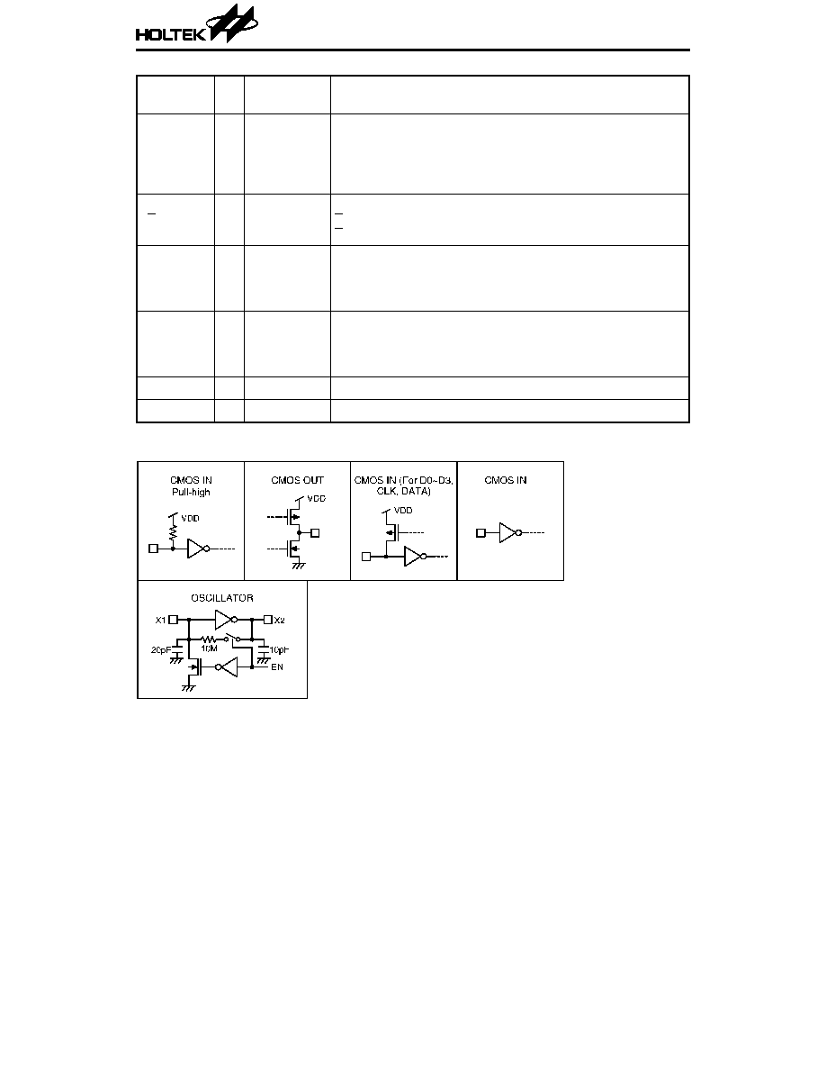
Pin Description
Pin Name
I/O
Internal
Connection
Description
CE
I
CMOS IN
Pull-high
Chip enable, active low
X2
O
Oscillator
The system oscillator consists of an inverter, a bias resistor, and
the required load capacitor on chip.
The oscillator function can be implemented by Connect a
standard 3.579545MHz crystal to the X1 and X2 terminals.
X1
I
VSS
--
--
Negative power supply
NC
--
--
No connection
HT9200A/B
2
21st Aug '98
Pin Name
I/O
Internal
Connection
Description
D0~D3
I
CMOS IN
Pull-high
or floating
Data inputs for the parallel mode
When the IC is operating in the serial mode, the data input
terminals (D0~D3) are included with a pull-high resistor. When
the IC is operating in the parallel mode, these pins become
floating.
S/P
I
CMOS IN
Operation mode selection input
S/P="H": Parallel mode
S/P="L": Serial mode
CLK
I
CMOS IN
Pull-high
or floating
Data synchronous clock input for the serial mode
When the IC is operating in the parallel mode, the input
terminal (CLK) is included with a pull-high resistor. When the
IC is operating in the serial mode, this pin becomes floating.
DATA
I
CMOS IN
Pull-high
or floating
Data input terminal for the serial mode
When the IC is operating in the parallel mode, the input terminal
(DATA) is included with a pull-high resistor. When the IC is
operating in the serial mode, this pin becomes floating.
DTMF
O
CMOS OUT
Output terminal of the DTMF signal
VDD
--
--
Positive power supply, 2.0V~5.5V for normal operation
Approximate internal connection circuits
HT9200A/B
3
21st Aug '98
Absolute Maximum Ratings*
Supply Voltage ................................. ≠0.3V to 6V
Storage Temperature................. ≠50
∞
C to 125
∞
C
Input Voltage.................... V
SS
≠0.3 to V
DD
+
0.3V
Operating Temperature............... ≠20
∞
C to 75
∞
C
*Note: These are stress ratings only. Stresses exceeding the range specified under "Absolute Maxi-
mum Ratings" may cause substantial damage to the device. Functional operation of this
device at other conditions beyond those listed in the specification is not implied and prolonged
exposure to extreme conditions may affect device reliability.
Electrical Characteristics
Ta=25
∞
C
Symbol
Parameter
Test Conditions
Min.
Typ.
Max.
Unit
V
DD
Conditions
V
DD
Operating Voltage
--
--
2
--
5.5
V
I
DD
Operating Current
2.5V S/P=V
DD
,D0~D3=V
SS
,
CE=V
SS
, No load
--
240
2500
µ
A
5.0V
--
950
3000
V
IL
"Low" Input Voltage
--
--
VSS
--
0.2V
DD
V
V
IH
"High" Input Voltage
--
--
0.8V
DD
--
V
DD
V
I
STB
Standby Current
2.5V S/P=V
DD
,CE=V
DD
,
No load
--
--
1
µ
A
5.0V
--
--
2
R
P
Pull-high Resistance
2.5V
V
OL
=0V
120
180
270
k
5.0V
45
68
100
t
DE
DTMF Output Delay
Time (Parallel Mode)
5V
--
--
t
UP
+6
t
UP
+8
ms
V
TDC
DTMF Output DC
Level
2V~
5.5V
DTMF Output
0.45V
DD
--
0.75V
DD
V
I
TOL
DTMF Sink Current
2.5V V
DTMF
=0.5V
≠0.1
--
--
mA
V
TAC
DTMF Output AC
Level
2.5V Row group, R
L
=5k
0.12
0.15
0.18
Vrms
A
CR
Column Pre-emphasis
2.5V Row group=0dB
1
2
3
dB
R
L
DTMF Output Load
2.5V t
HD
≠23dB
5
--
--
k
t
HD
Tone Signal
Distortion
2.5V R
L
=5k
--
≠30
≠23
dB
f
CLK
Clock Input Rate
(Serial Mode)
--
--
--
100
500
kHz
t
UP
Oscillator Starting
Time (When CE is low)
5.0V
The time from CE
falling edge to normal
oscillator operation
--
--
10
ms
f
OSC
System Frequency
--
Crystal=3.5795MHz
3.5759
3.5795
3.5831
MHz
HT9200A/B
4
21st Aug '98

Table 1: Digits vs. input data vs. tone output frequency (serial mode)
Digit
D4
D3
D2
D1
D0
Tone Output Frequency (Hz)
1
0
0
0
0
1
697
+
1209
2
0
0
0
1
0
697
+
1336
3
0
0
0
1
1
697
+
1477
4
0
0
1
0
0
770
+
1209
5
0
0
1
0
1
770
+
1336
6
0
0
1
1
0
770
+
1477
7
0
0
1
1
1
852
+
1209
8
0
1
0
0
0
852
+
1336
9
0
1
0
0
1
852
+
1477
0
0
1
0
1
0
941
+
1336
0
1
0
1
1
941
+
1209
#
0
1
1
0
0
941
+
1477
A
0
1
1
0
1
697
+
1633
B
0
1
1
1
0
770
+
1633
C
0
1
1
1
1
852
+
1633
D
0
0
0
0
0
941
+
1633
--
1
0
0
0
0
697
--
1
0
0
0
1
770
--
1
0
0
1
0
852
--
1
0
0
1
1
941
--
1
0
1
0
0
1209
--
1
0
1
0
1
1336
--
1
0
1
1
0
1477
--
1
0
1
1
1
1633
DTMF OFF
1
1
1
1
1
--
*Notes: The codes not listed in Table 1 are not used D4 is MSB
Functional Description
The HT9200A/B are DTMF generators for
µ
C
interfaces. They are controlled by a
µ
C in the
serial mode or the parallel mode (for the
HT9200B only).
Serial mode (HT9200A/B)
The HT9200A/B employ a data input, a 5-bit
code, and a synchronous clock to transmit a
DTMF signal. Every digit of a phone number to
be transmitted is selected by a series of inputs
which consist of 5-bit data. Of the 5 bits, the
D0(LSB) is the first received bit. The
HT9200A/B will latch data on the falling edge of
the clock (CLK pin). The relationship between
the digital codes and the tone output frequency
is shown in Table 1. As for the control timing
diagram, refer to Figure 1.
HT9200A/B
5
21st Aug '98