 | –≠–ª–µ–∫—Ç—Ä–æ–Ω–Ω—ã–π –∫–æ–º–ø–æ–Ω–µ–Ω—Ç: HT9320 | –°–∫–∞—á–∞—Ç—å:  PDF PDF  ZIP ZIP |
Document Outline
- ˛ˇ
- ˛ˇ
- ˛ˇ
- ˛ˇ
- ˛ˇ
- ˛ˇ
- ˛ˇ
- ˛ˇ
- ˛ˇ
- ˛ˇ
- ˛ˇ
- ˛ˇ
- ˛ˇ
- ˛ˇ

HT9320 Series
22-Memory Tone/Pulse Dialer
Rev. 1.10
1
October 1, 2002
Features
∑
Universal specification
∑
Operating voltag0e: 2.0V~5.5V
∑
Low standby current
∑
Lowmemoryretentioncurrent:0.1
mA(typ.)
∑
Tone/pulse switchable
∑
Interface with LCD driver
∑
32 digits for redialing
∑
32 digits for the SA memory dialing
∑
One-key redialing
∑
Pause and P
ÆT key for PBX
∑
3.58MHz crystal or ceramic resonator
∑
Hand-free control
∑
Hold-line control
∑
Pause, P
ÆT can be saved for redialing
∑
On-hook store function
∑
Keytone function
∑
Lock function
∑
Resistor options
-
M/B ratio
-
Flash function and flash time
-
Pause and P
ÆT duration
-
Pulse number
-
Inter-digit pause time for 10pps
∑
Memory number: 22 memories
∑
HT9320A/B/H/K/L-X: 28-pin DIP package
HT9320C: 22-pin SKDIP package
General Description
The HT9320 series tone/pulse dialers are CMOS LSI for
telecommunication systems. They are designed to meet
various dialing specifications through resistor option
matrix.
The HT9320 series are offered in six different versions.
The different functions of the six versions are listed in
the selection table. The HT9320A, HT9320H versions
provide the on-hook store function; the HT9320B ver-
sion provides the LCD interface function; the HT9320K
version provides the keytone function; the HT9320L ver-
sion provides both the LCD interface function and IDD
lock function. The six versions also supply the hold-line
and hand-free functions, which are suitable for feature
phone applications.
H T 9 3 2 0 s e r i e s p r o v i d e S A , R e d i a l a n d 2 0
one-touch/two-touch memory dialing. If the keyboard in-
cludes M1~M20 keys it can be used as one-touch mem-
ory dialing. Otherwise, it works as two-touch
(PAGE
ÆM1~M10) or three-touch(AÆPAGEÆ0~9)
memory dialing for speed dialing in either pulse or tone
mode.
Patent Number: 64097, 86474, 113235(R.O.C.), 5424740(U.S.A.)
Selection Table
Function
Memory
Dialing
Hold-
Line
Hand-
Free
LCD
Interface
Flash
Function
Flash
Time
(ms)
Pulse
No.
Tone
Dura-
tion
(ms)
Inter-
Tone-
Pause
(ms)
M/B
Pin
IDD
Lock
Key-
Tone
Output
On-
Hook
Store
Package
Part No.
HT9320A
SA, R
M1~M20
÷
÷
æ
Control
600
N, N+1
10
-N
82.5
85.5
÷
æ
æ
÷
28 DIP
Digit
600/300/98
HT9320B
SA, R
M1~M20
÷
÷
÷
Control
600
N, N+1
10
-N
82.5
85.5
æ
æ
æ
æ
28 DIP
Digit
600/300/98
HT9320C
SA, R
M1~M20
æ
æ
æ
Control
600
N, N+1
10
-N
82.5
85.5
æ
æ
æ
æ
22SKDIP
Digit
600/300/98
HT9320H
SA, R
M1~M20
÷
÷
æ
Digit
600/100
N
82.5
85.5
÷
æ
æ
÷
28 DIP
HT9320K
SA, R
M1~M20
÷
÷
æ
Control
600
N, N+1
10
-N
82.5
85.5
æ
æ
÷
æ
28 DIP
Digit
600/300/98
HT9320L
SA, R
M1~M20
÷
÷
÷
Control
600
N, N+1
10
-N
82.5
85.5
æ
÷
æ
æ
28 DIP
Digit
600/300/98
HT9320L-X
The same as HT9320L, but the voltage polarity of the row group and the column group are reversed.
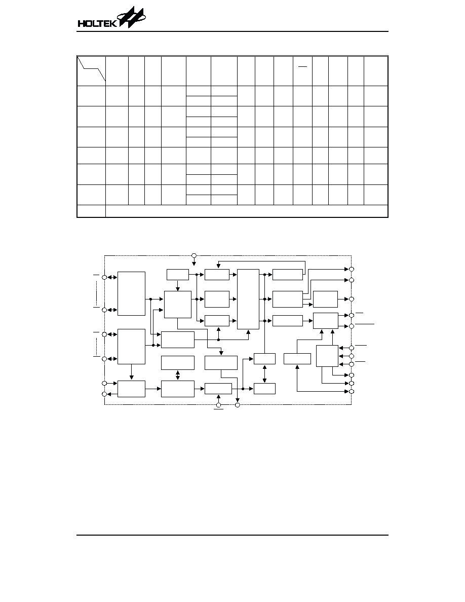
Block Diagram
HT9320 Series
Rev. 1.10
2
October 1, 2002
M / B
C 1
R 1
P O
H K S
H D I
K e y
C o l u m n
. S M
K e y
. u n c t i o n
E n c o d e r
E n c o d e r
C o n t r o l
W R M
C o u n t e r
A D D R L
K e y R o w
S R A M
D e b o u n c e
D i v i d e r
C l o c k
G e n e r a t o r
M / B
. l a s h
T i m e r
C h e c k
T o n e
E n c o d e r
C o n v e r t e r
M o d e I n
H D / H .
T o n e
O u t
P u l s e
O u t
X 1
X 2
D T M .
H . I
M O D E
H . O
H D O
D O U T
C L O C K
X M U T E
C 8
R 5
H S T
K e y t o n e
C i r c u i t
K T

Pin Assignment
Keyboard Information
HT9320A/B/C/K/L
HT9320H
HT9320 Series
Rev. 1.10
3
October 1, 2002
2 8
2 7
2 6
2 5
2 4
2 3
2 2
2 1
2 0
1 9
1 8
1 7
1 6
1 5
1
2
3
4
5
6
7
8
9
1 0
1 1
1 2
1 3
1 4
C 7
C 6
C 5
C 4
C 3
C 2
C 1
P O
H . O
X M U T E
D T M .
H D I
H D O
V S S
2 8
2 7
2 6
2 5
2 4
2 3
2 2
2 1
2 0
1 9
1 8
1 7
1 6
1 5
1
2
3
4
5
6
7
8
9
1 0
1 1
1 2
1 3
1 4
C 7
C 6
C 5
C 4
C 3
C 2
C 1
P O
H . O
X M U T E
D T M .
H D I
H D O
V S S
C 8
D O U T
R 1
R 2
R 3
R 4
R 5
H K S
C L O C K
H . I
M O D E
X 1
X 2
V D D
2 8
2 7
2 6
2 5
2 4
2 3
2 2
2 1
2 0
1 9
1 8
1 7
1 6
1 5
1
2
3
4
5
6
7
8
9
1 0
1 1
1 2
1 3
1 4
C 7
C 6
C 5
C 4
C 3
C 2
C 1
P O
H . O
X M U T E
D T M .
H D I
H D O
V S S
C 8
K T
R 1
R 2
R 3
R 4
R 5
H K S
N C
H . I
M O D E
X 1
X 2
V D D
C 8
H S T
R 1
R 2
R 3
R 4
R 5
H K S
M / B
H . I
M O D E
X 1
X 2
V D D
2 2
2 1
2 0
1 9
1 8
1 7
1 6
1 5
1 4
1 3
1 2
1
2
3
4
5
6
7
8
9
1 0
1 1
C 8
R 1
R 2
R 3
R 4
R 5
H K S
M O D E
X 1
X 2
V D D
C 7
C 6
C 5
C 4
C 3
C 2
C 1
P O
X M U T E
D T M .
V S S
H T 9 3 2 0 A / H
2 8 D I P - A
H T 9 3 2 0 B / L / L - X
2 8 D I P - A
H T 9 3 2 0 C
2 2 S K D I P - A
H T 9 3 2 0 K
2 8 D I P - A
C 1
C 2
C 3
C 4
C 5
C 6
R 1
R 2
R 3
R 4
R 5
C 1
C 2
C 3
C 4
C 5
C 7
C 8
C 6
R 1
R 2
R 3
R 4
R 5
∑ O n e - t o u c h m e m o r y k e y b o a r d
∑ T w o - t o u c h m e m o r y k e y b o a r d
∑ T h r e e - t o u c h m e m o r y k e y b o a r d
R 1
R 2
R 3
R 4
R 5
C 1
C 2
C 3
C 4
P
2
5
8
0
M 1 6
M 1 7
M 1 8
M 1 9
M 2 0
M 6
M 7
M 8
M 9
M 1 0
M 1 1
M 1 2
M 1 3
M 1 4
M 1 5
M 1
M 2
M 3
M 4
M 5
3
6
9
#
S A
1
4
7
* / T
M 6 /
M 7 /
M 8 /
M 9 /
M 1 0 /
M 1 6
M 1 7
M 1 8
M 1 9
M 2 0
M 1 1
M 1 2
M 1 3
M 1 4
M 1 5
M 1 /
M 2 /
M 3 /
M 4 /
M 5 /
P
2
5
8
0
P A G E
3
6
9
#
S A
1
4
7
* / T
.
A
S T
R
.
S T
R
.
S T
R
P
2
5
8
0
P A G E
3
6
9
#
S A
1
4
7
* / T
C 1
C 2
C 3
C 4
C 5
C 6
R 1
R 2
R 3
R 4
R 5
C 1
C 2
C 3
C 4
C 5
C 7
C 8
C 6
R 1
R 2
R 3
R 4
R 5
∑ O n e - t o u c h m e m o r y k e y b o a r d
∑ T w o - t o u c h m e m o r y k e y b o a r d
∑ T h r e e - t o u c h m e m o r y k e y b o a r d
R 1
R 2
R 3
R 4
R 5
C 1
C 2
C 3
C 4
2
5
8
0
M 1 6
M 1 7
M 1 8
M 1 9
M 2 0
M 6
M 7
M 8
M 9
M 1 0
M 1 1
M 1 2
M 1 3
M 1 4
M 1 5
M 1
M 2
M 3
M 4
M 5
3
6
9
#
S A
1
4
7
*
M 6 /
M 7 /
M 8 /
M 9 /
M 1 0 /
M 1 6
M 1 7
M 1 8
M 1 9
M 2 0
M 1 1
M 1 2
M 1 3
M 1 4
M 1 5
M 1 /
M 2 /
M 3 /
M 4 /
M 5 /
2
5
8
0
P A G E
3
6
9
#
S A
1
4
7
*
P Æ T
.
A
S T
R / P
2
5
8
0
P A G E
3
6
9
#
S A
1
4
7
*
P Æ T
.
A
S T
R / P
P Æ T
.
S T
R / P

Memory dialing vs. keyboard form table
Dialing Output
One-Touch
Memory Keyboard
Two-Touch
Memory Keyboard
Three-Touch
Memory Keyboard
M1~M10
M1 ~ M10
A
a (a=1~9, 0)
M11~M20
M11 ~ M20
PAGE Ma (Ma=M1~M10)
A PAGE a (a=1~9, 0)
Pin Description
Pin Name
I/O
Internal
Connection
Description
C1~C8
R1~R5
I/O
CMOS
IN/OUT
These pins form a 5
¥8 keyboard matrix which can perform keyboard input de-
tection and dialing specification setting functions. When on-hook (HKS=high)
all the pins are set high. While off-hook the column group (C1~C8) remains
low and the row group (R1~R5) is set high for key input detection.
For the HT9320L-X, the column group remains high and the row group is set
low for key input detection.
An inexpensive single contact 5
¥8 keyboard can be used as an input device.
Pressing a key connects a single column to a single row, and actuates the sys-
tem oscillator that results in a dialing signal output. If more than two keys are
pressed at the same time, no response occurs. The key-in debounce time is
20ms. Refer to the keyboard information for keyboard arrangement and to the
functional description for dialing specification selection.
X1
I
OSCILLATOR
The system oscillator consists of an inverter, a bias resistor and the necessary
load capacitor on chip. Connecting a standard 3.579545MHz crystal or ce-
ramic resonator to the X1 and X2 terminals can implement the oscillator func-
tion. The oscillator is turned off in the standby mode, and is actuated
whenever a keyboard entry is detected.
X2
O
XMUTE
O
NMOS OUT
XMUTE is an NMOS open drain structure pulled to VSS during dialing signal
transmission. Otherwise, it is an open circuit. XMUTE is used to mute the
speech circuit when transmitting the dial signal.
HKS
I
CMOS IN
This pin is used to monitor the status of the hook-switch and its combination
with HFI/HDI can control the PO pin output to make or break the line.
HKS=VDD: On-hook state (PO=low). Except for HFI/HDI (hand-free/hold-line
control input), other functions are all disabled.
HKS=VSS: Off-hook state (PO=high). The chip is in the stand-by mode and
ready to receive the key input.
PO
O
CMOS OUT
This pin is a CMOS output structure which by receiving the HKS and
HFO/HDO signals, control the dialer to connect or disconnect the telephone
line.
PO outputs a low to break line when HKS is high (on-hook) and HFO/HDO is
low. PO outputs a high to make line when HKS is low (off-hook) or HFO is high
or HDO is high.
During the off-hook state, this pin also outputs the dialing pulse train in pulse
mode dialing. While in the tone mode, this pin is always high.
MODE
I/O
CMOS IN/OUT
This is a three-state input/output pin, used for dialing mode selection, either
Tone mode or Pulse mode, 10pps/20pps
MODE=VDD: Pulse mode, 10pps
MODE=OPEN: Pulse mode, 20pps
MODE=VSS: Tone mode
During the pulse mode dialing, switching this pin to the tone mode changes
the subsequent digit entry to the tone mode. When the chips are in tone mode,
switching to the pulse mode will also be recognized.
DTMF
O
CMOS OUT
This pin is active only when the chip transmits tone dialing signals. Otherwise,
it always outputs a low. The pin outputs tone signals to drive the external
transmitter amplifier circuit. The load resistor should not be less than 5k
W.
HT9320 Series
Rev. 1.10
4
October 1, 2002

Pin Name
I/O
Internal
Connection
Description
HDI
I
CMOS IN
Pull-high
This pin is a Schmitt trigger input structure. Active low. Applying a negative going
pulse to this pin can toggle the HDO output once.
An external RC network is recommended for input debouncing. The pull-high
resistance is 200k
W typ.
HDO
O
CMOS OUT
The HDO is a CMOS output structure. Its output is toggle- controlled by a nega-
tive transition on HDI. When HDO is toggled high, PO keeps high to hold the line.
The hold function can be released by setting HFO high or by an on-off hook oper-
ation or by another HDI input. Refer to the functional description for the hold-line
function.
HFI
I
CMOS IN
Pull-low
This pin is a Schmitt trigger input structure. Active high. Applying a positive go-
ing pulse to HFI can toggle the HFO once and hence control the hand-free
function.
An external RC network is recommended for input debouncing. The pull-low
resistance of HFI is 200k
W typ.
HFO
O
CMOS OUT
The HFO is a CMOS output structure. Its output is toggle- controlled by a posi-
tive transition on the HFI pin. When HFO is high, the hand-free function is en-
abled and PO outputs a high to connect the line.
The hand-free function can be released by an on-off-hook operation or by
another HFI input or by setting HDO high. Refer to the functional description
for the hand-free function operation.
DOUT
O
NMOS OUT
NMOS open drain output pin. It outputs the BCD code of the dialing digits to
the LCD driver chip (HT16XX series) or MCU for dialing number display. Refer
to the functional description for the detailed timing.
CLOCK
O
NMOS OUT
NMOS open drain output. When dialing, it outputs a series of pulse trains for
DOUT data synchronization. DOUT data is valid at the falling edge of clock.
VDD
æ
æ
Positive power supply, 2.0V~5.5V for normal operation
VSS
æ
æ
Negative power supply, ground
HST
I
CMOS IN
Pull-low
(HT9320A)
On-hook store enable input
HST=VDD: On-hook store (HT9320A/H)
HST=Floating: Off-hook store (HT9320A)
HST=VSS: Off-hook store (HT9320H)
The Pull-low resistance is 200k
W typ.
CMOS IN
(HT9320H)
M/B
I
CMOS IN
Pull-high
(HT9320A)
Make/Break ratio selection
M/B=VSS: 33.3/66.6 (HT9320A)
M/B=Floating: 40/60 (HT9320A)
M/B=VDD: 33.3/66.6 (HT9320H)
M/B=VSS: 40/60 (HT9320H)
The pull-high resistance is 200k
W typ.
CMOS IN
(HT9320H)
KT
O
CMOS OUT
Keytone output pin. Outputs a 1.2kHz tone carrier for 34ms each time a key is
pressed in the pulse mode.
HT9320 Series
Rev. 1.10
5
October 1, 2002