
HI-1570
MIL-STD-1553 / 1760
5V Monolithic Dual Variable AmplitudeTransceiver
PIN CONFIGURATIONS
DESCRIPTION
bus
To minimize the package size for this function, the
transmitter outputs are internally connected to the
receiver inputs so that only two pins are required for
connection to each coupling transformer. For designs
requiring independent access to transmitter and receiver
1553 signals, please contact your Holt Sales
representative.
The HI-1570 is a low power CMOS dual +5V transceiver
with the ability to vary the amplitude of the transmitter
outputs. It is designed to meet the requirements of the
MIL-STD-1553 / 1760 specifications.
The transmitter section of each channel takes
complementary CMOS / TTL digital input data and
converts it to bi-phase Manchester encoded 1553 signals
suitable for driving the bus isolation transformer.
Separate transmitter inhibit control signals are provided
for each transmitter. A single pin allows the user to control
the transmitter output amplitude.
The receiver section of each channel converts the 1553
bi-phase
data to complementary CMOS / TTL data
suitable for inputting to a Manchester decoder. Each
receiver has a separate enable input which can be used to
force the output of the receiver to a logic "0".
V
A&B 1
BUSA 2
3
RXENA 4
GNDA 5
VDDA/B 6
BUSB 7
8
RXENB 9
GNDB 10
CONT
BUSA
BUSB
FEATURES
!
!
!
!
!
!
!
!
Compliant to MIL-STD-1553A & B,
MIL-STD-1760, ARINC 708A
CMOS technology for low standby power
Single +5V power supply
Variable transmitter output amplitude
Smallest footprint available in 20 pin plastic
ESOIC (thermally enhanced SOIC) package
Less than 1.0W maximum power dissipation
Military processing options
Industry standard pin configurations
20 Pin Ceramic DIP package
20
19 TXA
18 TXINHA
17 RXA
16
15
14 TXB
13 TXINHB
12 RXB
11
TXA
RXA
TXB
RXB
December 2002
(DS1570 Rev. B)
12/02
V
A&B 1
BUSA 2
3
RXENA 4
GNDA 5
VDDA/B 6
BUSB 7
8
RXENB 9
GNDB 10
CONT
BUSA
BUSB
20
19 TXA
18 TXINHA
17 RXA
16
15
14 TXB
13 TXINHB
12 RXB
11
TXA
RXA
TXB
RXB
20 Pin Plastic ESOIC - WB package
1570PSI
1570PST
1570PSM
1570CDI
1570CDT
1570CDM
HOLT INTEGRATED CIRCUITS
www.holtic.com
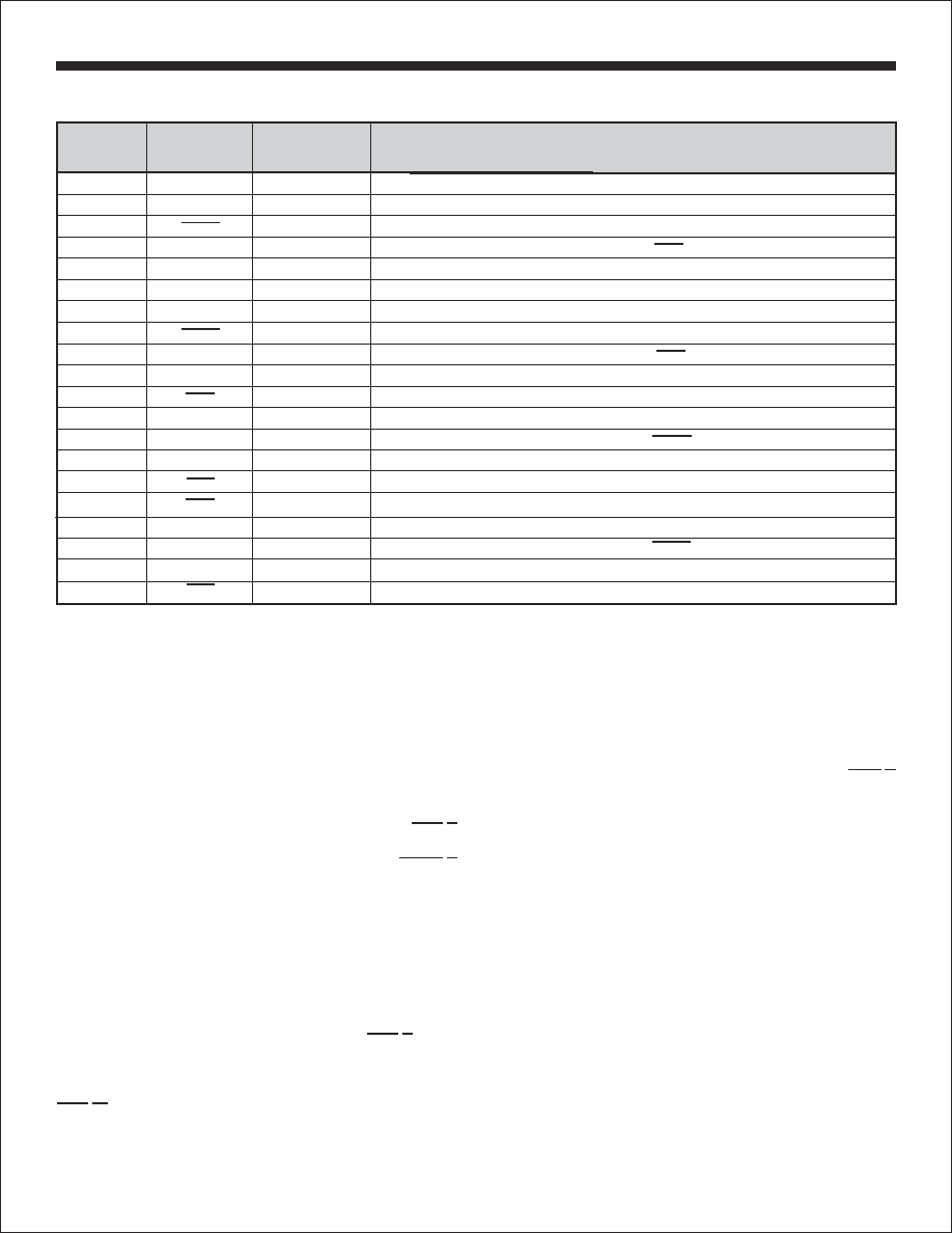
PIN DESCRIPTIONS
PIN
SYMBOL
FUNCTION
DESCRIPTION
1
V
A/B
analog Input
Transmit output amplitude control (0 - 5 Vdc, see Figure 4)
2
BUSA
analog output
MIL-STD-1533 bus driver A, positive signal
3
analog output
MIL-STD-1553 bus driver A, negative signal
4
RXENA
digital input
Receiver A enable. If low, forces RXA and
low
5
GNDA
power supply
Ground for channel A
6
VDDA/B
7
BUSB
9
RXENB
10
GNDB
11
12
RXB
digital output
Receiver B output, non-inverted
13
TXINHB
digital input
Transmit inhibit, channel B. If high BUSB,
disabled
14
TXB
digital input
Transmitter B digital data input, non-inverted
15
digital input
Transmitter B digital data input, inverted
16
digital output
CONT
BUSA
RXA
BUSB
TXB
RXA
power supply
+5 volt power for both channel A and channel B
analog output
MIL-STD-1533 bus driver B, positive signal
8
analog output
MIL-STD-1553 bus driver B, negative signal
digital input
Receiver B enable. If low, forces RXB and
low
power supply
Ground for channel B
digital output
Receiver B output, inverted
Receiver A output, inverted
17
RXA
digital output
Receiver A output, non-inverted
18
TXINHA
digital input
Transmit inhibit, channel A. If high BUSA,
disabled
19
TXA
digital input
Transmitter A digital data input, non-inverted
20
digital input
Transmitter A digital data input, inverted
BUSB
RXB
RXB
BUSA
TXA
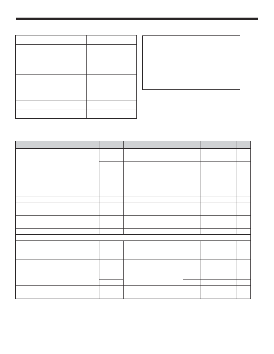
FUNCTIONAL DESCRIPTION
BUSA/B and
/
V
The transmitter is automatically inhibited and placed in the
high impedance state when both TXA/B and
/
are ei-
ther at a logic "1" or logic "0" simultaneously. A logic "1" ap-
plied to the TXINHA/B input will force the transmitter to the
high impedance state, regardless of the state of TXA/B and
/
BUSA B
TXA B
TXA B.
CONT
The HI-1570 data bus transceiver contains differential volt-
age source drivers and differential receivers. They are in-
tended for applications using a MIL-STD-1553 A/B data
bus. The device produces a trapezoidal output waveform
during transmission.
Data input to the device's transmitter section is from the
complementary CMOS / TTL inputs TXA/B and
/ .
The transmitter accepts Manchester II bi-phase data and
converts it to differential voltages on
.
The transceiver outputs are either direct or transformer cou-
pled to the MIL-STD-1553 data bus. Both coupling meth-
ods produce a nominal voltage on the bus of 7.5 volts peak
to peak at V
A&B = 5.0 Vdc. Refer to Figure 4 for
transmitter output amplitudes at other values of
A&B between 0 - 5 Vdc. (Contact your Holt Sales Repre-
sentative about the 0 - 10 Vdc Control Voltage option).
TRANSMITTER
TXA B
CONT
RECEIVER
The receiver accepts bi-phase differential data from the
MIL-STD-1553 bus through the same direct or transformer
coupled interface as the transmitter. The receiver's differ-
ential input stage drives a filter and threshold comparator
that produces CMOS/TTL data at the RXA/B and
/
output pins.
RXA B
Each set of receiver outputs can be independently forced
to a logic "0" by setting RXENA or RXENB low.
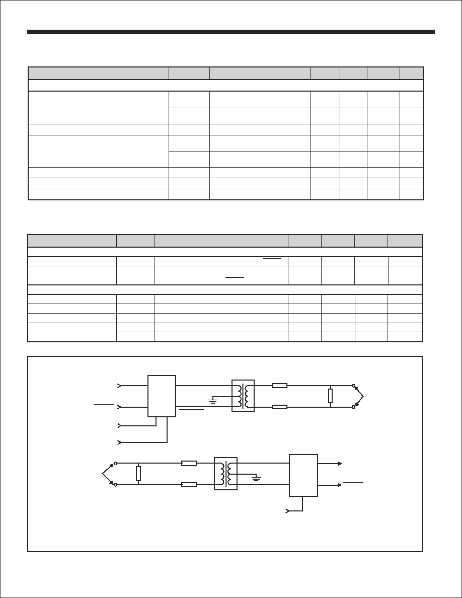
A direct coupled interface (see Figure 2) uses a 1:2.5 ratio
isolation transformer and two 55 ohm isolation resistors
between the transformer and the bus.
In a transformer coupled interface (see Figure 3), the
transceiver is connected to a 1:1.79 isolation transformer
which in turn is connected to a 1:1.4 coupling transformer.
The transformer coupled method also requires two
coupling resistors equal to 75% of the bus characteristic
impedance (Zo) between the coupling transformer and the
bus.
MIL-STD-1553 BUS INTERFACE
HI-1570
HOLT INTEGRATED CIRCUITS
2

TRANSMIT WAVEFORM - EXAMPLE PATTERN
TXA/B
TXA/B
BUSA/B - BUSA/B
RECEIVE WAVEFORMS - EXAMPLE PATTERN
RXA/B
RXA/B
Vin
(Line to Line)
Figure 1. Block Diagram
V
A&B
CONT
TXA/B
TXINHA/B
RXA/B
RXA/B
RXENA/B
Each Channel
Transmit
Logic
Receive
Logic
Slope
Control
Comparator
Input
Filter
BUSA/B
BUSA/B
TRANSMITTER
RECEIVER
Data Bus
Isolation
Transformer
Coupler
Network
Direct or
Transformer
HI-1570
TXA/B
HOLT INTEGRATED CIRCUITS
3
PARAMETER
SYMBOL
CONDITION
MIN
TYP
MAX
UNITS
Operating Voltage
VDD
4.75
5
5.25
V
Total Supply Current
ICC1
Not Transmitting
20
30
mA
ICC2
Transmit one channel @
340
mA
50% duty cycle
ICC3
Transmit one channel @
550
mA
100% duty cycle
Power Dissipation
PD1
Not Transmitting
0.11
W
PD2
Transmit one channel @
0.70
0.95
W
100% duty cycle
Min. Input Voltage
(HI)
V
Digital inputs
2.0
1.4
V
Max. Input Voltage
(LO)
V
Digital inputs
1.4
0.8
V
Min. Input Current
(HI)
I
V
= 4.9V, Digital inputs
20
�A
Max. Input Current
(LO)
I
V
= 0.1V, Digital inputs
-20
�A
Min. Output Voltage
(HI)
V
I
= -0.4mA, Digital outputs
2.7
V
Max. Output Voltage
(LO)
V
I
= 4.0mA, Digital outputs
0.4
V
Input resistance
R
Differential
20
K
Input capacitance
C
Differential
5
pF
Common mode rejection ratio
CMRR
40
dB
Input Level
V
Differential
9
Vp-p
Input common mode voltage
V
-5.0
5.0
V-pk
Threshold Voltage - Direct-coupled
Detect
1.15
20.0
No Detect
0.28
Threshold Voltage -
Detect
0.86
14.0
No Detect
0.20
200
400
V
1 Mhz Sine Wave
Vp-p
V
(Measured at Point "A " in Figure 2)
Vp-p
Transformer-coupled
V
1 MHz Sine Wave
Vp-p
V
(Measured at Point "A " in Figure 3)
Vp-p
IH
IL
IH
IH
IL
IL
OH
OUT
IH
OUT
D
RECEIVER
(Measured at Point "A " in Figure 2 unless otherwise specified)
IN
IN
IN
ICM
W
THD
THND
THD
THND
D
T
NOTE:
Stresses above absolute maximum
ratings or outside recommended operating
conditions may cause permanent damage to the
device. These are stress ratings only. Operation
at the limits is not recommended.
Supply voltage (
Logic input voltage range
Power dissipation at 25�C
1.0 W
ceramic DIL, derate
7mW/�C
Solder Temperature
275�C for 10 sec.
Junction Temperature
175�C
Storage Temperature
-65�C to +150�C
VDD)
-0.3 V to +7 V
-0.3 V dc to +5.5 V
Receiver differential voltage
10 Vp-p
Driver peak output current
+1.0 A
ABSOLUTE MAXIMUM RATINGS
RECOMMENDED OPERATING CONDITIONS
Supply Voltage
Temperature Range
Industrial Screening.........-40�C to +85�C
Hi-Temp Screening........-55�C to +125�C
Military Screening..........-55�C to +125�C
VDD....................................... 5V... �5%
DC ELECTRICAL CHARACTERISTICS
VDD = 5.0V, GND = 0V, V
A/B = 5.0V, T = Operating Temperature Range (unless otherwise specified).
CONT
A
HI-1570
HOLT INTEGRATED CIRCUITS
4
PARAMETER
SYMBOL
TEST CONDITIONS
MIN
TYP
MAX
UNITS
Receiver Enable Delay
tREN
From RXENA/B rising or falling edge to
40
ns
RXA/B or
Driver Delay
tDT
TXA/B, TXA/B to BUSA/B, BUSA/B
150
ns
Rise time
tr
35 ohm load
100
300
ns
Fall Time
tf
35 ohm load
100
300
ns
Inhibit Delay
tDI-H
Inhibited output
100
ns
tDI-L
Active output
150
ns
RECEIVER
TRANSMITTER
(Measured at Point "A " in Figure 2)
(Measured at Point "A " in Figure 2)
D
D
Receiver Delay
tDR
From input zero crossing to RXA/B or
450
ns
RXA/B
RXA/B
AC ELECTRICAL CHARACTERISTICS
VDD = 5.0V, GND = 0V, V
A/B = 5.0V, T =Operating Temperature Range (unless otherwise specified).
CONT
A
PARAMETER
SYMBOL
CONDITION
MIN
TYP
MAX
UNITS
Output Voltage
Direct coupled
35
load
7.0
9.0
Vp-p
(Measured at Point "A " in Figure 2)
70
20.0
27.0
Vp-p
Output Noise
V
Differential, inhibited
10.0
mVp-p
Output Dynamic Offset Voltage
V
-90
90
mV
-250
250
mV
Output Resistance
R
Differential, not transmitting
10
K
Output Capacitance
C
1 MHz sine wave
15
pF
Control Line Resistance
R
5
TRANSMITTER
(Measured at Point "A " in Figure 2 unless otherwise specified)
D
D
V
Transformer coupled
V
load
(Measured at Point "A " in Figure 3)
Direct coupled
35
load
(Measured at Point "A " in Figure 2)
Transformer coupled
V
70
load
(Measured at Point "A " in Figure 3)
K
OUT
OUT
DYN
W
W
W
T
D
T
ON
DYN
OUT
OUT
CONT
W
W
W
DC ELECTRICAL CHARACTERISTICS (cont.)
VDD = 5.0V, GND = 0V, V
A/B = 5.0V, T = Operating Temperature Range (unless otherwise specified).
CONT
A
TXA/B
TXA/B
V
A&B
CONT
TRANSMITTER
RECEIVER
1:2.5
Point "A "
D
55
W
55
W
35
W
2.5:1
55
W
55
W
35
W
RXENA/B
BUSA/B
BUSA/B
RXA/B
RXA/B
Figure 2. Direct Coupled Test Circuits
HI-1570
Isolation
Transformer
Isolation
Transformer
Point "A "
D
TXINHA/B
2.5:1
HOLT INTEGRATED CIRCUITS
5