
HI-3282
GENERAL DESCRIPTION
The HI-3282 is a silicon gate CMOS device for interfacing
the ARINC 429 serial data bus to a 16-bit parallel data bus.
Two receivers and an independent transmitter are
provided. The receiver input circuitry and logic are
designed to meet the ARINC 429 specifications for loading,
level detection, timing, and protocol.
The transmitter
section provides the ARINC 429 communication protocol.
Additional interface circuitry such as the Holt HI-8382 or HI-
8585 are required to translate the 5 volt logic outputs to
ARINC 429 drive levels.
The 16-bit parallel data bus exchanges the 32-bit ARINC
data word in two steps when either loading the transmitter
or interrogating the receivers. The data bus interfaces with
CMOS and TTL.
Timing of all the circuitry begins with the master clock input,
CLK. For ARINC 429 applications, the master clock
frequency is 1 MHz.
Each independent receiver monitors the data stream with a
sampling rate 10 times the data rate. The sampling rate is
software selectable at either 1MHz or 125KHz. The results
of a parity check are available as the 32nd ARINC bit.
The transmitter has a First In, First Out (FIFO) memory to
store 8 ARINC words for transmission. The data rate of the
transmitter is software selectable by dividing the master
clock, CLK, by either 10 or 80. The master clock is used to
set the timing of the ARINC transmission within the required
resolution.
APPLICATIONS
!
!
!
Avionics data communication
Serial to parallel conversion
Parallel to serial conversion
FEATURES
!
!
!
!
!
!
!
!
!
!
ARINC specification 429 compatible
16-Bit parallel data bus
Direct receiver interface to ARINC bus
Timing control 10 times the data rate
Selectable data clocks
Automatic transmitter data timing
Self test mode
Parity functions
Low power, single 5 volt supply
Industrial & full military temperature ranges
!
!
Compatible with Industry-standard alternate
Parts
Small footprint 44 PQFP package option
33 - N/C
32 - N/C
31 -
X
30 - ENTX
29 -
28 -429DO
27 - TX/R
26 -
25 -
24 - BD00
23 - BD01
CWSTR
429DO
PL2
PL1
N/C - 1
- 2
- 3
SEL - 4
- 5
- 6
BD15 - 7
BD14 - 8
BD13 - 9
BD12 - 10
BD11 - 11
D/R1
D/R2
EN1
EN2
HI-3282PQI
&
HI-3282PQT
HOLT INTEGRATED CIRCUITS
1
(DS3282 Rev. E)
05/01

SYMBOL
FUNCTION
DESCRIPTION
VCC
POWER
+5V �5%
429DI1 (A)
INPUT
ARINC receiver 1 positive input
429DI1 (B)
INPUT
ARINC receiver 1 negative input
429DI2 (A)
INPUT
ARINC receiver 2 positive input
429DI2 (B)
INPUT
ARINC receiver 2 negative input
OUTPUT
Receiver 1 data ready flag
OUTPUT
Receiver 2 data ready flag
SEL
INPUT
Receiver data byte selection (0 = BYTE 1) (1 = BYTE 2)
INPUT
Data Bus control, enables receiver 1 data to outputs
INPUT
Data Bus control, enables receiver 2 data to outputs if
is high
BD15
I/O
Data Bus
BD14
I/O
Data Bus
BD13
I/O
Data Bus
BD12
I/O
Data Bus
BD11
I/O
Data Bus
BD10
I/O
Data Bus
BD09
I/O
Data Bus
BD08
I/O
Data Bus
BD07
I/O
Data Bus
BD06
I/O
Data Bus
GND
POWER
0 V
BD05
I/O
Data Bus
BD04
I/O
Data Bus
BD03
I/O
Data Bus
BD02
I/O
Data Bus
BD01
I/O
Data Bus
BD00
I/O
Data Bus
INPUT
Latch enable for byte 1 entered from data bus to transmitter FIFO.
INPUT
Latch enable for byte 2 entered from data bus to transmitter FIFO. Must follow
TX/R
OUTPUT
Transmitter ready flag. Goes low when ARINC word loaded into FIFO. Goes high
after transmission and FIFO empty.
429DO
OUTPUT
"ONES" data output from transmitter.
OUTPUT
"ZEROES" data output from transmitter.
ENTX
INPUT
Enable Transmission
INPUT
Clock for control word register
CLK
INPUT
Master Clock input
TX CLK
OUTPUT
Transmitter Clock equal to Master Clock (CLK), divided by either 10 or 80.
INPUT
Master Reset, active low
INPUT
Data bit control Enable. (Active low, with internal pull up to VDD).
D/R1
D/R2
EN1
EN2
EN1
PL1
PL2
PL1.
429DO
CWSTR
MR
DBCEN
PIN DESCRIPTION
HI-3282
HOLT INTEGRATED CIRCUITS
2

FUNCTIONAL DESCRIPTION
CONTROL WORD REGISTER
The HI-3282 contains 11 data flip flops whose D inputs are con-
nected to the data bus and clocks connected to
. Each
flip flop provides options to the user as follows:
CWSTR
THE RECEIVERS
ARINC BUS INTERFACE
Figure 1 shows the input circuit for each receiver. The ARINC 429
specification requires the following detection levels:
The HI-8382 guarantees recognition of these levels with a common
mode Voltage with respect to GND less than �5V for the worst case
condition (4.75V supply and 13V signal level).
The tolerances in the design guarantee detection of the above
levels, so the actual acceptance ranges are slightly larger. If the
ARINC signal is out of the actual acceptance ranges, including the
nulls, the chip rejects the data.
STATE
DIFFERENTIAL VOLTAGE
ONE
+6.5 Volts to +13 Volts
NULL
+2.5 Volts to -2.5 Volts
ZERO
-6.5 Volts to -13 Volts
BYTE 2
DATA
BD BD BD BD BD BD BD BD BD BD BD BD BD BD BD BD
BUS
15
14
13
12
11
10
09
08
07
06
05
04
03
02
01
00
ARINC
29
28
27
26
25
24
23
22
21
20
19
18
17
16
15
14
BIT
ARINC 429 DATA FORMAT
The following table shows the bit positions in exchanging data with
the receiver or the transmitter. ARINC bit 1 is the first bit
transmitted or received.
DATA
BD BD BD BD BD BD BD BD BD BD BD BD BD BD BD BD
BUS
15
14
13
12
11
10
09
08
07
06
05
04
03
02
01
00
ARINC
13
12
11
10
9
31
30
32
1
2
3
4
5
6
7
8
BIT
BYTE 1
HI-3282
DATA
BUS
FUNCTION
CONTROL
DESCRIPTION
PIN
BD04
PAREN
Enables parity bit insertion into
Transmitter data bit 32
If enabled, an internal connection
BDO5
SELF TEST
0 = ENABLE
is made passing 429DO and
to the receiver logic inputs
RECEIVER 1
If enabled, ARINC bits 9 and,
BDO6
DECODER
1 = ENABLE
10 must match the next two
control word bits
If Receiver 1 Decoder is
BDO7
-
-
enabled, the ARINC bit 9
must match this bit
If Receiver 1 Decoder is
BDO8
-
-
enabled, the ARINC bit 10
must match this bit
RECEIVER 2
If enabled, ARINC bits 9 and
BDO9
DECODER
1 = ENABLE
10 must match the next two
control word bits
If Receiver 2 Decoder is
BD10
-
-
enabled, then ARINC bit 9
must match this bit
If Receiver 2 Decoder is
BD11
-
-
enabled, then ARINC bit 10
must match this bit
INVERT
Logic 0 enables normal odd parity
BD12
XMTR
1 = ENABLE
and Logic 1 enables even parity
PARITY
output in transmitter 32nd bit
BD13
XMTR DATA
0 = �10
CLK is divided either by 10 or
CLK SELECT
1 = �80
80 to obtain XMTR data clock
BD14
RCVR DTA
0 = �10
CLK is divided either by 10 or
CLK SELECT
1 = �80
80 to obtain RCVR data clock
429DO
HOLT INTEGRATED CIRCUITS
3
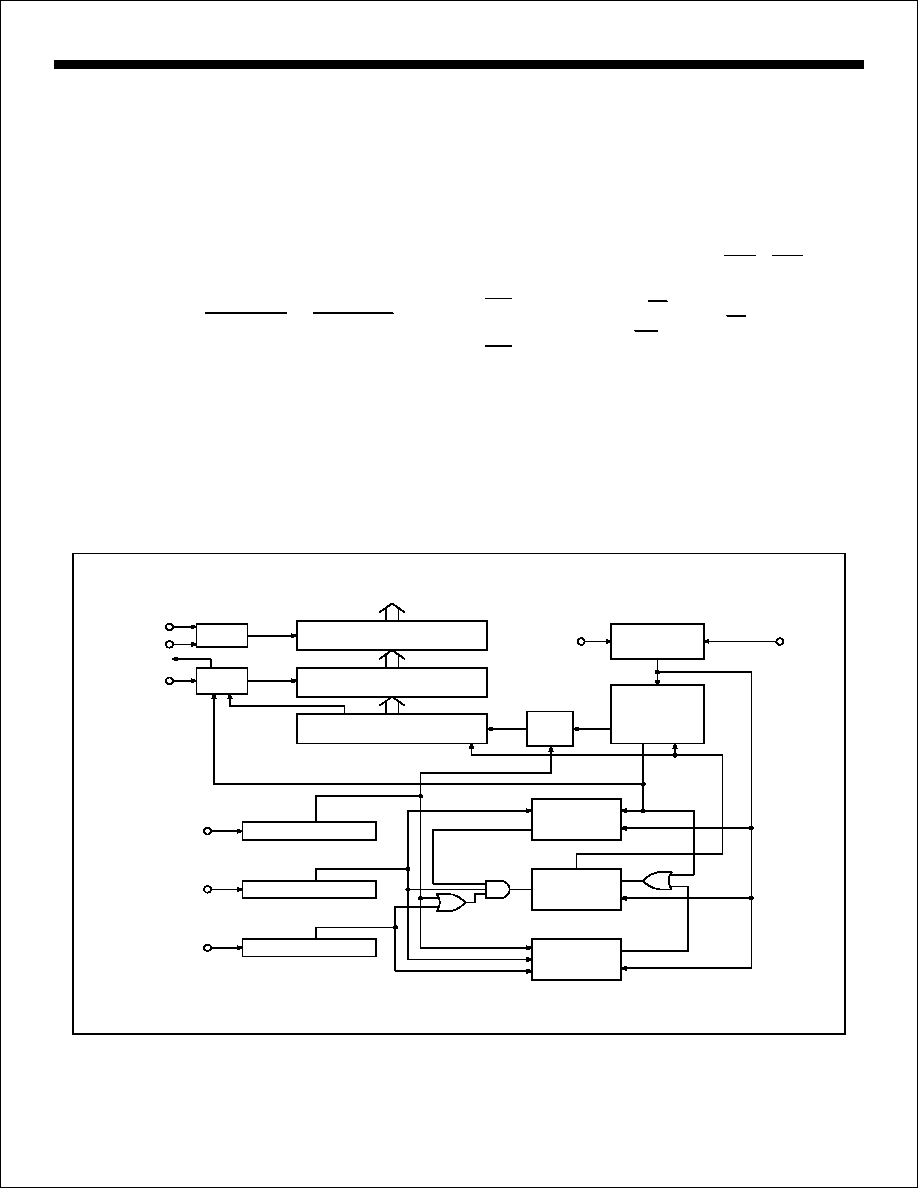
RECEIVER LOGIC OPERATION
BIT TIMING
Figure 2 shows a block diagram of the logic section of each receiver.
The ARINC 429 specification contains the following timing
specification for the received data:
100K BPS � 1%
12K -14.5K BPS
1.5 � 0.5 �sec
10 � 5 �sec
1.5 � 0.5 �sec
10 � 5 �sec
5 �sec � 5%
34.5 to 41.7 �sec
BIT RATE
PULSE RISE TIME
PULSE FALL TIME
PULSEWIDTH
HIGH SPEED
LOW SPEED
FUNCTIONAL DESCRIPTION (con't)
The receiver parity circuit counts Ones received, including the
parity bit, ARINC bit 32. If the result is odd, then "0" will appear in
the 32nd bit.
RECEIVER PARITY
RETRIEVING DATA
Once 32 valid bits are recognized, the receiver logic generates
an End of Sequence (EOS). If the receiver decoder is enabled
and the 9th and 10th ARINC bits match the control word
program bits or if the receiver decoder is disabled, then EOS
clocks the data ready flag flip flop to a "1",
or
(or both)
will go low. The data flag for a receiver will remain low until after
ARINC bytes from that receiver are retrieved.
This is
accomplished by activating
with SEL, the byte selector, low
to retrieve the first byte and activating
with SEL high to
retrieve the second byte.
retrieves data from receiver 1 and
retrieves data from receiver 2.
If another ARINC word is received, and a new EOS occurs
before the two bytes are retrieved, the data is overwritten by the
new word.
D/R1
D/R2
EN
EN
ENI
EN2
both
SEL
EN
D/R
DECODER
CONTROL
BITS
/
MUX
CONTROL
LATCH
ENABLE
CONTROL
32 TO 16 DRIVER
32 BIT LATCH
32 BIT SHIFT REGISTER
TO PINS
CONTROL
BIT BD14
CLOCK
OPTION
CLOCK
CLK
BIT
COUNTER
AND
END OF
SEQUENCE
PARITY
CHECK
32ND
BIT
DATA
BIT CLOCK
EOS
WORD GAP
WORD GAP
TIMER
BIT CLOCK
END
START
SEQUENCE
CONTROL
ERROR
CLOCK
ERROR
DETECTION
SHIFT REGISTER
SHIFT REGISTER
NULL
ZEROS
SHIFT REGISTER
ONES
EOS
BITS 9 & 10
FIGURE 2.
RECEIVER BLOCK DIAGRAM
HI-3282
HOLT INTEGRATED CIRCUITS
4

TRANSMITTER
A block diagram of the transmitter section is shown in Figure 3.
The FIFO is loaded sequentially by first pulsing
to load byte 1
and then
to load byte 2. The control logic automatically loads
the 31 bit word in the next available position of the FIFO. If TX/R,
the transmitter ready flag is high (FIFO empty), then 8 words,
each 31 bits long, may be loaded. If TX/R is low, then only the
available positions may be loaded. If all 8 positions are full, the
FIFO ignores further attempts to load data.
When ENTX goes high, enabling transmission, the FIFO
positions are incremented with the top register loading into the
data transmission shift register. Within 2.5 data clocks the first
data bit appears at either 429DO or
. The 31 bits in the
data transmission shift register are presented sequentially to the
outputs in the ARINC 429 format with the following timing:
ARINC DATA BIT TIME
10 Clocks
80 Clocks
DATA BIT TIME
5 Clocks
40 Clocks
NULL BIT TIME
5 Clocks
40 Clocks
WORD GAP TIME
40 Clocks
320 Clocks
The word counter detects when all loaded positions are
transmitted and sets the transmitter ready flag, TX/R, high.
FIFO OPERATION
DATA TRANSMISSION
PL1
PL2
429DO
HIGH SPEED
LOW SPEED
TRANSMITTER PARITY
Control register bit BD04 (PAREN) enables parity bit insertion into
transmitter data bit 32. Parity is always inserted if DBCEN is open
or high. If DBCEN is low, logic 0 on PAREN inserts data on bit 32,
and logic 1 on PAREN inserts parity on bit 32.
The parity generator counts the ONES in the 31-bit word. If the
BD12 control word bit is set low, the 32nd bit transmitted will make
parity odd. If the control bit is high the parity is even.
If the BD05 control word bit is set low, 429DO or
become
inputs to the receivers bypassing the interface circuitry.
outputs remain active during self test.
The two receivers are independent of the transmitter. Therefore,
control of data exchanges are strictly at the option of the user. The
only restrictions are:
1. The received data may be overwritten if not retrieved
within one ARINC word cycle.
2. The FIFO can store 8 words maximum and ignores
attempts to load addition data if full.
3. Byte 1 of the transmitter data must be loaded first.
4. Either byte of the received data may be retrieved first.
Both bytes must be retrieved to clear the data ready flag.
5. After ENTX, transmission enable, goes high it cannot go
low until TX/R, transmitter readyflag, goes high. Otherwise,
one ARINC word is lost during transmission.
SELF TEST
SYSTEM OPERATION
429DO
429DO
and 429DO
HI-3282
HOLT INTEGRATED CIRCUITS
5