 | –≠–ª–µ–∫—Ç—Ä–æ–Ω–Ω—ã–π –∫–æ–º–ø–æ–Ω–µ–Ω—Ç: HI-8382UT | –°–∫–∞—á–∞—Ç—å:  PDF PDF  ZIP ZIP |
HI-8382, HI-8383
The HI-8382 and HI-8383 bus interface products are silicon
gate CMOS devices designed as a line driver in accordance with
the ARINC 429 bus specifications.
Inputs are provided for clocking and synchronization. These
signals are AND'd with the DATA inputs to enhance system
performance and allow the HI-8382 to be used in a variety of
applications.
Both logic and synchronization inputs feature
built-in 2,000V minimum ESD input protection as well as TTL
and CMOS compatibility.
The differential outputs of the HI-8382 are independently
programmable to either the high speed or low speed ARINC 429
output rise and fall time specifications through the use of two
external capacitors. The output voltage swing is also adjustable
by the application of an external voltage to the VREF input. The
HI-8382 has on-chip Zener diodes in series with a fuse to each
differential output protecting the ARINC bus from an overvoltage
failure. The outputs each have a series resistance of 37.5 ohms.
The HI-8383 is identical to the HI-8382 except that the series
resistors are 13 ohms and the overvoltage protection circuitry
has been eliminated.
The HI-8382 and HI-8383 are intended for use where logic
signals must be converted to ARINC 429 levels such as a user
ASIC or the HI-8282 ARINC 429 Serial Transmitter/Dual
Receiver or the HI-6010 ARINC 429 Transmitter/Receiver. Holt
products are readily available for both industrial and military
applications. Please contact the Holt Sales Department for
additional information, including data sheets for the HI-8282 and
HI-6010 products.
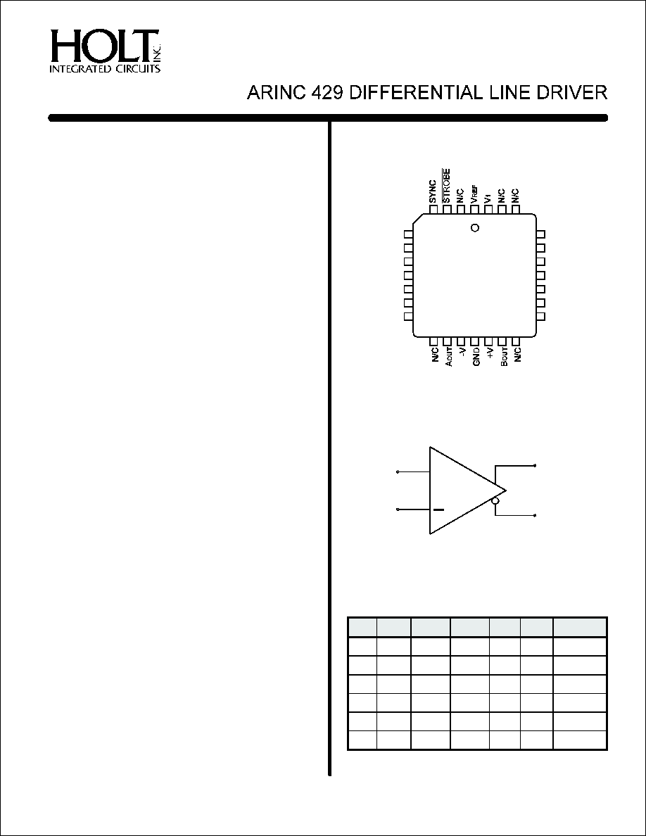
PIN CONFIGURATION
(Top View)
GENERAL DESCRIPTION
!
!
!
!
!
!
!
!
Low power CMOS
TTL and CMOS compatible inputs
Programmable output voltage swing
Adjustable ARINC rise and fall times
Operates at data rates up to 100 Kbits
Overvoltage protection
Industrial and Military temperature ranges
DSCC SMD part number
FEATURES
4
3
2
1
28
27
26
12 13
14
15
16
17
18
5
6
7
8
9
10
11
25
24
23
22
21
20
19
CLOCK
N/C
DATA (B)
C
N/C
N/C
N/C
B
N/C
DATA (A)
N/C
N/C
C
N/C
N/C
A
HI-8382J
28 - PIN
PLASTIC
PLCC
FUNCTION
ARINC 429 DIFFERENTIAL LINE DRIVER
H I - 8 3 8 2
+
TRUTH TABLE
SYNC CLOCK DATA(A) DATA(B) AOUT
BOUT COMMENTS
X
L
X
X
0V
0V
NULL
L
X
X
X
0V
0V
NULL
H
H
L
L
0V
0V
NULL
H
H
L
H
-V
+V
LOW
H
H
H
L
+V
-V
HIGH
H
H
H
H
0V
0V
NULL
REF
REF
REF
REF
(See Page 4-46 for additional package pin configurations)
January 2001
HOLT INTEGRATED CIRCUITS
1
(DS8382 Rev. A)
01/01
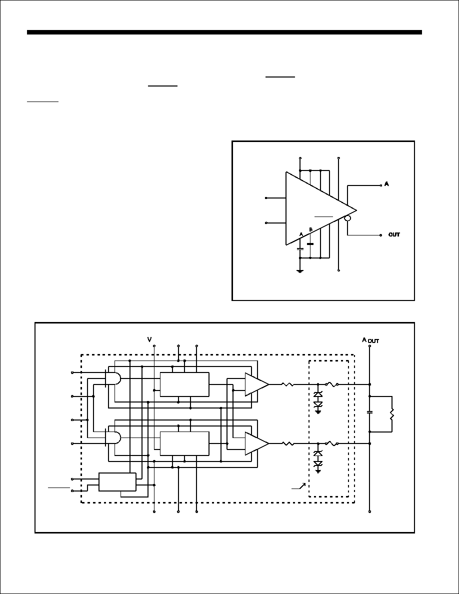
FUNCTIONAL DESCRIPTION
The SYNC and CLOCK inputs establish data synchronization
utilizing two AND gates, one for each data input. Each logic
input, including the power enable (
) input, are
TTL/CMOS compatible. Besides reducing chip current drain,
also floats each output. However the overvoltage
fuses and diodes of the HI-8382 are not switched out.
Figure 1 illustrates a typical ARINC 429 bus application.
Three power supplies are necessary to operate the HI-8382;
typically +15V, -15V and +5V. The chip also works with ±12V
supplies. The +5V supply can also provide a reference
voltage that determines the output voltage swing.
The
differential output voltage swing will equal 2V
. If a value of
V
other than +5V is needed, a separate +5V power supply
is required for pin V .
With the DATA (A) input at a logic high and DATA (B) input at a
logic low, A
will switch to the +V
rail and B
will
switch to the -V
rail (ARINC HIGH state). With both data
input signals at a logic low state, the outputs will both switch to
0V (ARINC NULL state).
The driver output impedance, R
, is nominally 75 ohms.
The rise and fall times of the outputs can be calibrated through
the selection of two external capacitor values th
re
connected to the C and C input pins. Typical values for
high-speed operation (100KBPS) are C = C = 75pF and for
low-speed operation (12.5 to 14KBPS) C = C = 500pF.
STROBE
STROBE
REF
REF
OUT
REF
OUT
REF
OUT
1
A
B
A
B
A
B
at a
The driver can be externally powered down by applying a logic
high to the
input pin. If this feature is not being used,
the pin should be tied to ground.
The C
and C
pins are inputs to unity gain amplifiers.
Therefore they must be allowed to swing to -5V. Provision to
switch capacitors must be done with analog switches that
allow voltages below their ground.
STROBE
A
B
Figure 2. FUNCTIONAL BLOCK DIAGRAM
DATA (A)
OUT
DATA (B)
INPUTS
TO ARINC BUS
B
REF
V
1
V
SYNC
CLOCK
-V
+V
STROBE
GND
C
C
-15V
+15V
+5V
HI-8382, HI-8383
Figure 1. ARINC 429 BUS APPLICATION
DATA (A)
DATA (B)
SYNC
CLOCK
V
1
STROBE
LEVEL SHIFTER
AND SLOPE
CONTROL (A)
LEVEL SHIFTER
AND SLOPE
CONTROL (B)
CURRENT
REGULATOR
OUTPUT
DRIVER (B)
OUTPUT
DRIVER (A)
R
/2
OUT
R
/2
OUT
F
A
F
B
OVER VOLTAGE
CLAMPS
C
L
R
L
OUT
B
B
C
GND
-V
A
C
+V
REF
Not included on HI-8383
HOLT INTEGRATED CIRCUITS
2
All Voltages referenced to GND, TA = Operating Temperature Range (unless otherwise specified)
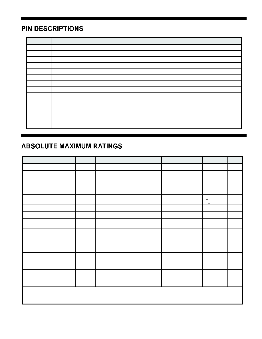
SYMBOL
FUNCTION
DESCRIPTION
V
POWER
THE REFERENCE VOLTAGE USED TO DETERMINE THE OUTPUT VOLTAGE SWING
INPUT
A LOGIC HIGH ON THIS INPUT PLACES THE DRIVER IN POWER DOWN MODE
SYNC
INPUT
SYNCHRONIZES DATA INPUTS
DATA (A)
INPUT
DATA INPUT TERMINAL A
C
INPUT
CONNECTION FOR DATA (A) SLEW-RATE CAPACITOR
A
OUTPUT
ARINC OUTPUT TERMINAL A
-V
POWER
-12V to -15V
GND
POWER
0.0V
+V
POWER
+12V to +15V
B
OUTPUT
ARINC OUTPUT TERMINAL B
C
INPUT
CONNECTION FOR DATA (B) SLEW-RATE CAPACITOR
DATA (B)
INPUT
DATA INPUT TERMINAL B
CLOCK
INPUT
SYNCHRONIZES DATA INPUTS
V
POWER
+5V ±5%
REF
A
OUT
OUT
B
1
STROBE
PARAMETER
SYMBOL
CONDITIONS
OPERATING RANGE
MAXIMUM
UNIT
Differential Voltage
V
Voltage between +V and -V terminals
40
V
Supply Voltage
+V
+10.8 to +16.5
V
-V
-10.8 to -16.5
V
V
+5 ±10%
+7
V
Voltage Reference
V
For ARINC 429
+5 ±5%
6
V
For Applications other than ARINC
0 to 6
6
V
Input Voltage Range
V
GND -0.3
V
V1 +0.3
V
Output Short-Circuit Duration
See Note: 1
Output Overvoltage Protection
See Note: 2
Operating Temperature Range
T
Hi-temp & Military
-55 to +125
∞C
Industrial
-40 to +85
∞C
Storage Temperature Range
T
Ceramic & Plastic
-65 to +150
∞C
Lead Temperature
Soldering, 10 seconds
+275
∞C
Junction Temperature
T
+175
∞C
Power Dissipation
P
16-Pin Ceramic DIP
See Note: 3
1.725
W
28-Pin Ceramic LCC
See Note: 3
1.120
W
28-Pin Plastic PLCC
See Note: 3
2.143
W
32-Pin CERQUAD
See Note: 3
1.725
W
Thermal Resistance,
ÿ
16-Pin Ceramic DIP
86.5
∞C/W
(Junction-to-Ambient)
28-Pin Ceramic LCC
133.7
∞C/W
28-Pin Plastic PLCC
70.0
∞C/W
32-Pin CERQUAD
86.5
∞C/W
Note 1. Heatsinking may be required for Output Short Circuit at +125∞C and for 100KBPS at +125∞C.
Note 2. The fuses used for Output Overvoltage Protection may be blown by the presence of a voltage at either output that is greater
than ±12.0V with respect to GND. (HI-8382 only)
Note 3. Derate above +25∞C, 11.5mW/∞C for 16-PIN DIP and 32-PIN CERQUAD, 7.5 mW/∞C for 28-PIN LCC, 14.2 mW/∞C for 28-PIN PLCC
DIF
1
REF
IN
A
STG
J
D
JA
>
<
NOTE: Stresses above those listed under "Absolute Maximum Ratings" may cause permanent damage to the device. These are stress ratings
only. Functional operation of the device at these or any other conditions above those indicated in the operational sections of the specifications
is not implied. Exposure to absolute maximum rating conditions for extended periods may affect device reliability.
HI-8382, HI-8383
HOLT INTEGRATED CIRCUITS
3

PARAMETER
SYMBOL
CONDITION
MIN
TYP
MAX UNITS
Supply Current +V (Operating)
(+V)
No Load
(0 - 100KBPS)
+11
mA
Supply Current -V (Operating)
(-V)
No Load
(0 - 100KBPS)
-11
mA
Supply Current
(Operating)
(
)
No Load
(0 - 100KBPS)
500
µA
Supply Current
(Operating)
(
)
No Load
(0 - 100KBPS)
500
µA
Supply Current +V (Power Down)
(+V)
STROBE = HIGH
475
uA
Supply Current -V (Power Down)
(-V)
STROBE = HIGH
-475
uA
Supply Current +V (During Short Circuit Test)
(+V)
Short to Ground
(See Note: 1)
150
mA
Supply Current -V (During Short Circuit Test)
(-V)
Short to Ground
(See Note: 1)
-150
mA
Output Short Circuit Current (Output High)
Short to Ground
=0 (See Note: 2)
-80
mA
Output Short Circuit Current (Output Low)
Short to Ground
=0 (See Note: 2)
+80
mA
Input Current (Input High)
1.0
µA
Input Current (Input Low)
-1.0
µA
Input Voltage High
2.0
V
Input Voltage Low
0.5
V
Output Voltage High (Output to Ground)
No Load
(0 -100KBPS)
+V
+V
V
-.
+.
Output Voltage Low (Output to Ground)
No Load
(0 -100KBPS)
-V
-V
V
-.
+.
Output Voltage Null
No Load
(0-100KBPS)
-250
+250
mV
Input Capacitance
15
pF
I
I
V
I
V
V
I
V
I
I
I
I
I
V
I
V
I
I
V
V
V
V
V
C
CCOP
CCOP
1
CCOP
1
REF
CCOP
REF
CCPD
CCPD
SC
SC
OHSC
MIN
OLSC
MIN
IH
IL
IH
IL
OH
25
25
OL
25
25
NULL
IN
See Note 1
REF
REF
REF
REF
Note 1. Not tested, but characterized at initial device design and after major process and/or design change which affects this parameter.
Note 2. Interchangeability of force and sense is acceptable.
+V = +15V, -V = -15V, V = V
= +5.0V, T
= Operating Temperature Range (unless otherwise specified).
1
REF
A
PARAMETER
SYMBOL
CONDITION
MIN
TYP
MAX UNITS
Rise Time (
,
)
=
= 75pF
See Figure 3.
1.0
2.0
µs
Fall Time (
,
)
=
= 75pF
See Figure 3.
1.0
2.0
µs
Propagtion Delay Input to Output
=
= 75pF
See Figure 3.
3.0
µs
Propagtion Delay Input to Output
=
= 75pF
See Figure 3.
3.0
µs
A
B
t
C
C
A
B
t
C
C
t
C
C
t
C
C
OUT
OUT
R
A
B
OUT
OUT
F
A
B
PLH
A
B
PHL
A
B
Figure 3. SWITCHING WAVEFORMS
-9.5V to -10.5V
+9.5V to +10.5V
-4.75V to -5.25V
2.0V
+4.75V to +5.25V
2.0V
0.5V
0.5V
-4.75V to -5.25V
+4.75V to +5.25V
DATA (A) 0V
DATA (B) 0V
A
OUT
0V
B
OUT
0V
DIFFERENTIAL
OUTPUT 0V
(
)
A
B
OUT -
OUT
50%
50%
V
REF
ADJUST
BY
C
A
t
PHL
ADJUST
BY
C
A
-V
REF
50%
50%
t
PLH
t
R
+V
REF
-V
REF
ADJUST
BY
C
B
ADJUST
BY
C
B
t
F
2V
REF
-2V
RE
HIGH
NULL
LOW
NOTE: OUTPUTS UNLOADED
HI-8382, HI-8383
+V = +15V, -V = -15V, V = V
= +5.0V, T
= Operating Temperature Range (unless otherwise specified).
1
REF
A
HOLT INTEGRATED CIRCUITS
4
NUMBER
DESCRIPTION
RANGE
FLOW
IN
FINISH
HI-8382C
16 PIN CERAMIC SIDE BRAZED DIP
-40∞C TO +85∞C
I
NO
GOLD
HI-8382CT
16 PIN CERAMIC SIDE BRAZED DIP
-55∞C TO +125∞C
T
NO
GOLD
HI-8382CM-01 16 PIN CERAMIC SIDE BRAZED DIP
-55∞C TO +125∞C
M
YES
SOLDER
HI-8382CM-03* 16 PIN CERAMIC SIDE BRAZED DIP
-55∞C TO +125∞C
DSCC
YES
SOLDER
HI-8382J
28 PIN PLASTIC J -LEAD PLCC
-40∞C TO +85∞C
I
NO
SOLDER
HI-8382JT
28 PIN PLASTIC J -LEAD PLCC
-55∞C TO +125∞C
T
NO
SOLDER
HI-8382S
28 PIN CERAMIC LEADLESS CHIP CARRIER
-40∞C TO +85∞C
I
NO
GOLD
HI-8382ST
28 PIN CERAMIC LEADLESS CHIP CARRIER
-55∞C TO +125∞C
T
NO
GOLD
HI-8382SM-01 28 PIN CERAMIC LEADLESS CHIP CARRIER
-55∞C TO +125∞C
M
YES
SOLDER
HI-8382U
32 PIN J-LEAD CERQUAD
-40∞C TO +85∞C
I
NO
SOLDER
HI-8382UT
32 PIN J-LEAD CERQUAD
-55∞C TO +125∞C
T
NO
SOLDER
HI-8382, HI-8383
HI-8383 part numbers identical except the SMD version is not available.
SUPPLY CURRENT (m A )
2
JUNCTION TEMP, Tj (∞C)
Ta = 25
o
C
Ta = 85
o
C
Ta=125
o
C
Ta = 25
o
C
Ta = 85
o
C
Ta=125
o
C
Low Speed
3
17.6
17.2
17.0
48
107
142
High Speed
4
25.4
24.5
24.2
56
110
150
Low Speed
17.9
17.4
17.1
41
103
145
High Speed
25.8
24.8
24.4
47
112
147
SUPPLY CURRENT (m A )
2
JUNCTION TEMP, Tj (∞C)
Ta = 25
o
C
Ta = 85
o
C
Ta=125
o
C
Ta = 25
o
C
Ta = 85
o
C
Ta=125
o
C
Low Speed
3
60.1
55.7
52.4
110
157
194
High Speed
4
63.1
56.3
52.3
100
150
182
Low Speed
62.1
56.2
53.0
90
145
180
High Speed
64.0
56.2
52.2
86
144
176
16 Le a d Ceramic SB DIP
PACKAGE STYLE
1
16 Le a d Ceramic SB DIP
M AXIM U M AR INC LOAD
7
A
OUT
and B
OUT
Shorted to Ground
5 , 6, 7
ARINC 429
DATA RATE
ARINC 429
DATA RATE
PACKAGE STYLE
1
28 Le a d PLCC
28 Le a d PLCC
Notes:
1. All data taken
on devices soldered to a single layer copper PCB (3" X 4.5" X .062").
2. At 100% duty cycle, 15V power supplies. For 12V power supplies multiply all tabulated values by 0.8.
3. Low Speed: Data Rate = 12.5 Kbps, Load: R = 400 Ohms, C = 30 nF.
4. High Speed: Data Rate = 100 Kbps, Load: R = 400 Ohms, C = 10 nF. Data not presented for C = 30
as this is considered unrealistic for high speed operation.
5. Similar results would be obtained with A
shorted to B
.
6. For applications requiring survival with continuous short circuit, operation above Tj = 175∞C is not recommended.
7. Data will vary depending on air flow and the method of heat sinking employed.
in still air
OUT
OUT
HI-8382 PACKAGE THERMAL CHARACTERISTICS
HOLT INTEGRATED CIRCUITS
5