 | –≠–ª–µ–∫—Ç—Ä–æ–Ω–Ω—ã–π –∫–æ–º–ø–æ–Ω–µ–Ω—Ç: HI-8588 | –°–∫–∞—á–∞—Ç—å:  PDF PDF  ZIP ZIP |

HI-8588
DESCRIPTION
!
!
!
!
!
Direct ARINC 429 line receiver interface
in a small outline package
Receiver input hystersis at least 2 volts
Test inputs that bypass analog input and
can power down and tri-state outputs
Plastic and ceramic package options -
surface mount and DIP
Mil processing available
FEATURES
PIN CONFIGURATION
SUPPLY VOLTAGES
FUNCTION TABLE
RINA
GND
ROUTA
ROUTB
TESTB
TESTA
VCC
RINB
2
3
4
5
6
7
8
1
vcc
= 5.0V ± 5%
PIN
SYMBOL
FUNCTION
DESCRIPTION
VCC
SUPPLY
5 VOLT SUPPLY
TESTA
LOGIC INPUT
CMOS
RINB
ARINC INPUT
RECEIVER B INPUT
RINA
ARINC INPUT
RECEIVER A INPUT
GND
POWER
GROUND
ROUTA
LOGIC OUTPUT
RECEIVER CMOS OUTPUT A
ROUTB
LOGIC OUTPUT
RECEIVER CMOS OUTPUT B
TESTB
LOGIC INPUT
CMOS
PIN DESCRIPTION TABLE
The HI-8588 is an ARINC 429 bus interface receiver and is
available in a SO 8 pin package.
The technology is
analog/digital CMOS. The circuitry requires only a 5 volt
supply.
The ARINC bus can be connected directly to the chip. The
typical 10 volt differential signal is translated and input to a
window comparator and latch. The comparator levels are
just below the standard 6.5 volt minimum ARINC data
threshold and just above the standard 2.5 volt maximum
ARINC null threshold.
The TESTA and TESTB inputs bypass the analog for
testing purposes.
Also if TESTA and TESTB are both
taken high, the analog powers down and the digital outputs
tri-state allowing wire-or possibilities.
Please refer to the HI-8588-10 for applications where an
external resistance in series with the ARINC inputs is
required for lightning protection or when the digital outputs
need to be a logic zero rather than open circuit when
TESTA and TESTB are both high.
January 2001
(DS8588 Rev. A)
01/01
HOLT INTEGRATED CIRCUITS
1
HI-8588
FUNCTIONAL DESCRIPTION
RINA
RINB
NULL
ZERO
NULL
ONE
TEST
TESTA
TEST
TEST
TESTB
TESTA
'
TESTB
ROUTB
TESTA
'
TESTB
ROUTA
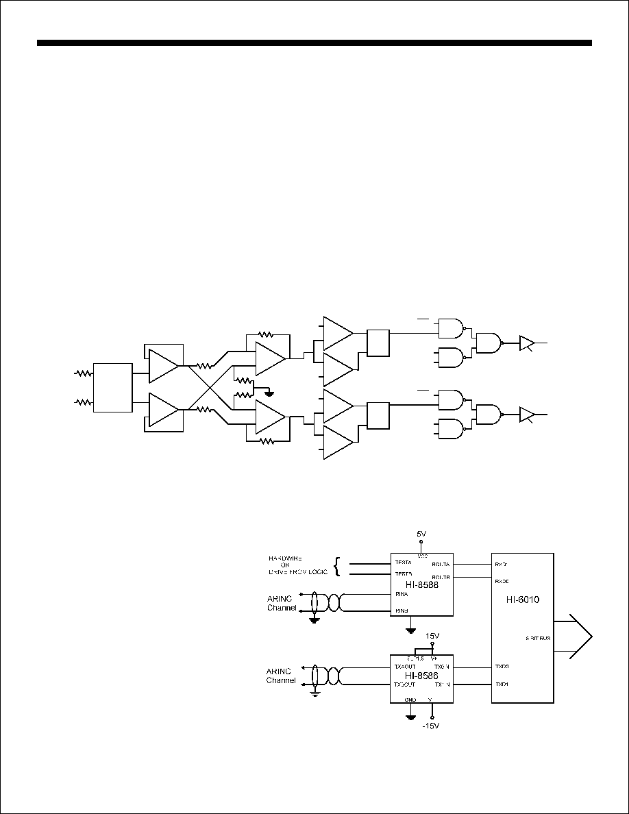
FIGURE 1 - RECEIVER BLOCK DIAGRAM
TEST
R
S
Q
R
LATCH
S
Q
LATCH
ESD
PROTECTION
AND
TRANSLATION
1
2
8
6
7
4
3
4
5
6
7
2
3
FIGURE 2 - APPLICATION DIAGRAM
APPLICATION INFORMATION
8
5
1
RECEIVER
Figure 1 shows the general architecture of the ARINC 429
receiver. The receiver operates off the VCC supply only.
The inputs RINA and RINB each have series resistors, typi-
cally 35K ohms. They connect to level translators whose
resistance to Ground is typically 10K ohms. Therefore, any
series resistance added to the inputs will affect the voltage
translation.
After level translation, the inputs are buffered and become
inputs to a differential amplifier. The amplitude of the dif-
ferential signal is compared to levels derived from a di-
vider between VCC and Ground. The nominal settings cor-
respond to a One/Zero amplitude of 6.0V and a Null ampli-
tude of 3.3V.
The status of the ARINC receiver input is latched. A Null
input resets the latches and a One or Zero input sets the
latches.
The logic at the output is controlled by the test signal
which is generated by the logical OR of theTestA and
TestB pins. If TestA and TestB are both One, then the re-
ceiver is powered down and the output pins float.
The
powerdown does not disconnect the internal resistors at
the ARINC input.
Figure 2 shows a possible application of the
HI-8588 interfacing an ARINC receive channel
to the HI-6010 which in turn interfaces to an
8-bit bus.
HOLT INTEGRATED CIRCUITS
2

HI-8588
Voltages referenced to Ground
Supply voltages
VCC...................................................7V
ARINC input - pins 3 & 4
Voltage at either pin......+29V to -29V
DC current per input pin................ ±10mA
Power dissipation at 25∞C
plastic DIL............0.7W
ceramic DIL..........0.5W
Solder Temperature ........275∞C for 10 sec
Storage Temperature........-65∞C to +150∞C
ABSOLUTE MAXIMUM RATINGS
RECOMMENDED OPERATING CONDITIONS
Supply Voltages
VCC........................................5V... ± 5%
Temperature Range
Industrial Screening........-40∞C to +85∞C
Hi-Temp Screening.......-55∞C to +125∞C
Military Screening.........-55∞C to +125∞C
supplies floating
Kohm
Kohm
"
"
V
VIN
IN = 5 V
= 0 V
µ
A
µ
A
V
= 4.6V
OH
V
= 0.4V
OL
mA
mA
mA
mA
OPERATING TEMPERATURE RANGE,
pins 2, 8 = 0V; pins 3, 4 open
pins 2, 8 = 5V; pins 3, 4 open
NOTE:
Stresses above absolute maximum
ratings or outside recommended operating con-
ditions may cause permanent damage to the
device. These are stress ratings only. Opera-
tion at the limits is not recommended.
HOLT INTEGRATED CIRCUITS
3

OPERATING TEMPERATURE RANGE,
HI-8588
defined in Figure 3, C = 50pF
L
DIFF
0V
0V
1
-10V
5V
0V
t rr
t rr
t fr
t
10%
90%
t phlr
t
t plhr
t
5V
0V
t plhr
t
t phlr
t
pin 6
pin 7
FIGURE 3 - RECEIVER TIMING
PART
PACKAGE
TEMPERATURE
BURN
LEAD
NUMBER
DESCRIPTION
RANGE
FLOW
IN
FINISH
HI-8588PDI
8 PIN PLASTIC DIP
-40∞C TO +85∞C
I
NO
SOLDER
HI-8588PDT
8 PIN PLASTIC DIP
-55∞C TO +125∞C
T
NO
SOLDER
HI-8588PSI
8 PIN PLASTIC NARROW BODY SOIC
-40∞C TO +85∞C
I
NO
SOLDER
HI-8588PST
8 PIN PLASTIC NARROW BODY SOIC
-55∞C TO +125∞C
T
NO
SOLDER
HI-8588CDI
8 PIN CERAMIC SIDE BRAZED DIP
-40∞C TO +85∞C
I
NO
GOLD
HI-8588CDT
8 PIN CERAMIC SIDE BRAZED DIP
-55∞C TO +125∞C
T
NO
GOLD
HI-8588CDM 8 PIN CERAMIC SIDE BRAZED DIP
-55∞C TO +125∞C
M
YES
SOLDER
HI-8588CRI
8 PIN CERDIP
-40∞C TO +85∞C
I
NO
SOLDER
HI-8588CRT
8 PIN CERDIP
-55∞C TO +125∞C
T
NO
SOLDER
HI-8588CRM 8 PIN CERDIP
-55∞C TO +125∞C
M
YES
SOLDER
HOLT INTEGRATED CIRCUITS
4
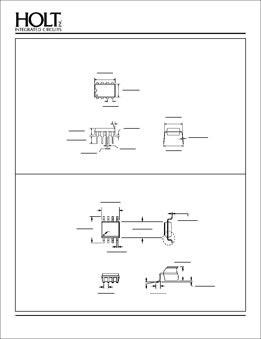
Package Type:
8-PIN PLASTIC DIP
8P
.385
±
.015
(4.699
±
.381)
7
∞
TYP.
.025
±
.010
(.635 ± .254)
.335
±
.035
(8.509
±
.889)
.250 ± .010
(6.350
±
.254)
.100
±
.010
(3.540
±
.254)
.135
±
.015
(3.429
±
.381)
.055
±
.010
(1.397
±
.254)
.1375
±
.0125
(3.493
±
.318)
.019
±
.002
(.483
±
.102)
.0115
±
.0035
(.292
±
.089)
.300
±
.010
(7.620
±
.254)
HI-8588 PACKAGE DIMENSIONS
inches (millimeters)
HOLT INTEGRATED CIRCUITS
5
Package Type:
Detail A
0
∞
to 8
∞
Detail A
8HN
8-PIN PLASTIC SMALL OUTLINE (SOIC) - NB
(Narrow Body)
IN
P
1
.236 ± .008
(5.994 ± .203)
.1535 ± .0035
(3.90 ± .09)
.1935 ± .0035
(4.915 ± .085)
.0086 ± .0012
(.2184 ± .0305)
.050 ± .010
(1.27 ± .254)
.033 ± .017
(.8382 ± .4318)
.055 ± .005
(1.397 ± .127)
.0069 ± .0029
(.1753 ± .0737)
.0165 ± .0035
(.4191 ± .0889)
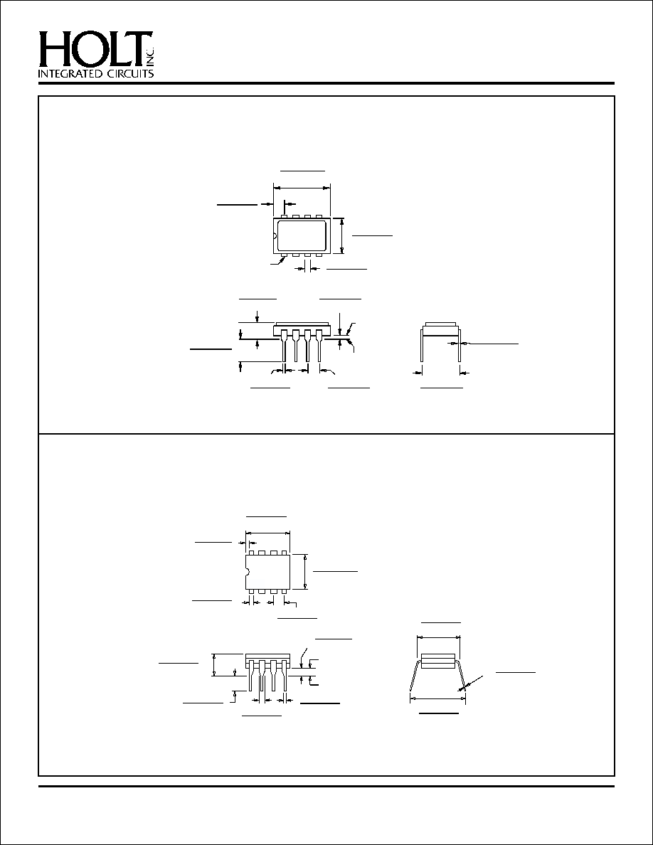
HI-8588 PACKAGE DIMENSIONS
inches (millimeters)
Package Type:
Package Type:
8-PIN CERAMIC SIDE-BRAZED DIP
8C
.405
±
MAX
(10.287
±
MAX)
PIN 1
.050
±
.007
(1.270
±
.178)
.200 MAX
(5.080 MAX)
.163 ± .037
(4.140
±
.940
)
.035 ± .010
(.889
±
.254)
.018 ± .002
(.457
±
.051)
.300 ± .010
(7.620
±
.254)
.0105
±
.0015
(.267
±
.038)
BASE
PLANE
.250
±
.008
(7.366
±
.203)
.050
±
.005
(1.270
±
.127)
SEATING
PLANE
.100 ± .003
(2.540
±
.076)
8D
8-PIN CERDIP
.380
±
.004
(9.652
±
.102)
.005 MIN.
(.127 MIN.)
.314
±
.003
(7.976
±
.076)
.200 MAX.
(5.080 MAX.)
.248
±
.003
(6.299
±
.076)
.100
±
.008
(2.540
±
.203)
.039
±
.006
(.991
±
.154)
.163
±
.037
(4.140
±
.940)
.018
±
.006
(.457
±
.152)
.056
±
.006
(1.422
±
.152)
.015 MIN.
(.381 MIN.)
.350
±
.030
(8.890
±
.762)
.010
±
.006
(.254
±
.152`)
Base Plane
Seating Plane
HOLT INTEGRATED CIRCUITS
6