HI-8581, HI-8589
ARINC 429 LINE DRIVER AND DUAL RECEIVER
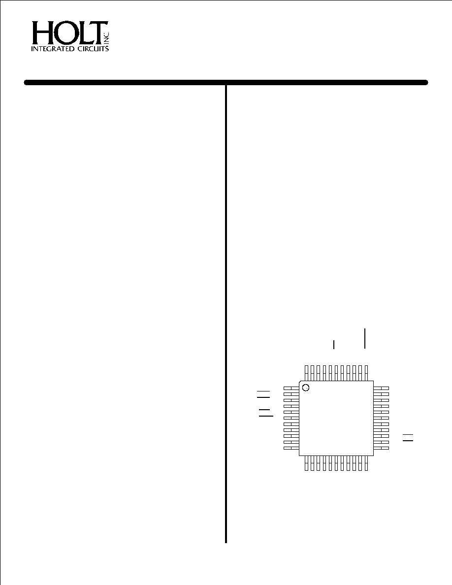
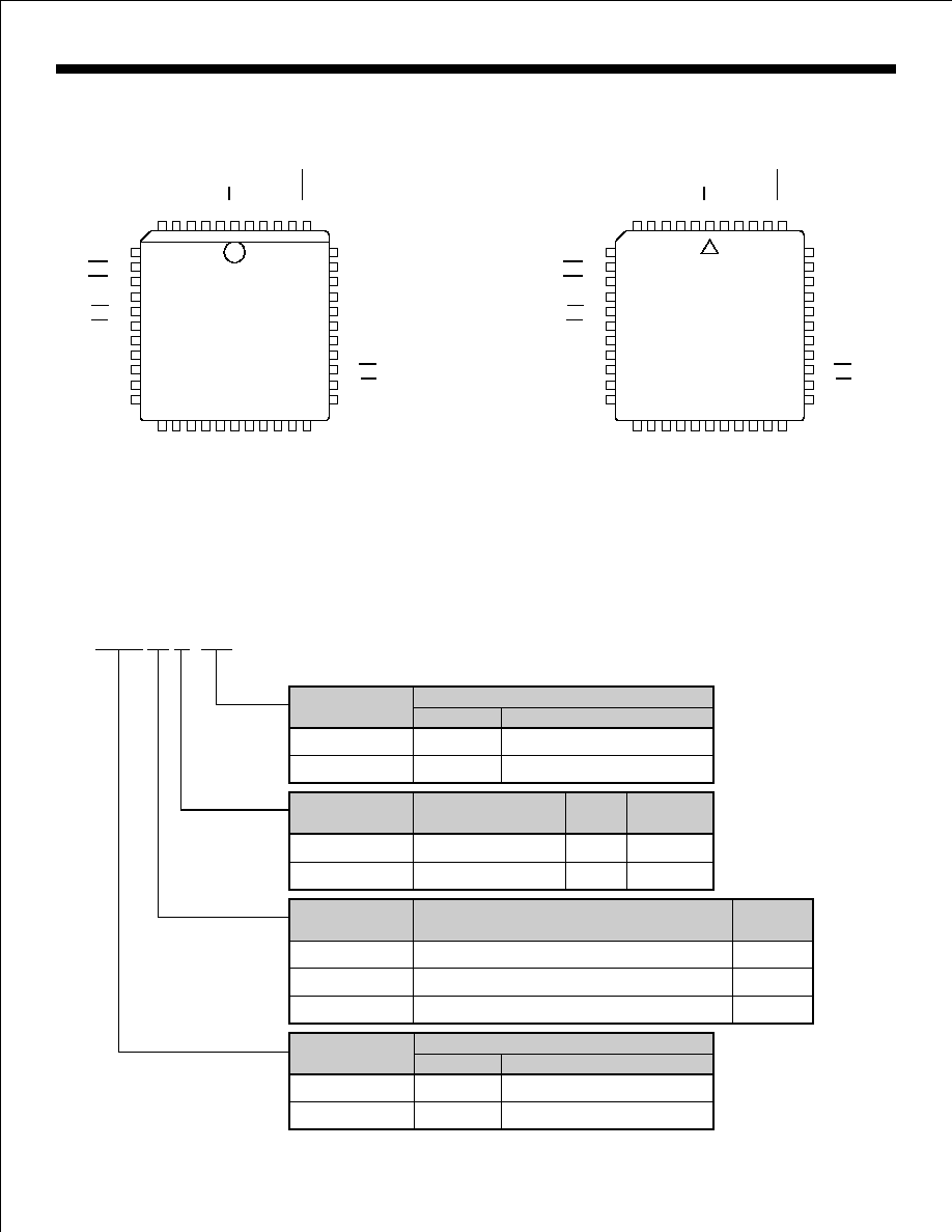
PIN CONFIGURATION
(Top View)
GENERAL DESCRIPTION
The HI-8581 and HI-8589 from Holt Integrated Circuits are
silicon gate CMOS devices for interfacing a 16-bit parallel
data bus directly to the ARINC 429 serial bus.
Both
devices provide two receivers, an independent transmitter
and line driver capability in a single package. The receiver
input circuitry and logic are designed to meet the
ARINC 429 specifications for loading, level detection,
timing, and protocol. The transmitter section provides the
ARINC 429 communication protocol and the line driver
circuits provide the ARINC 429 output levels.
The 16-bit parallel data bus exchanges the 32-bit ARINC
data word in two steps when either loading the transmitter
or interrogating the receivers.
The data bus interfaces
with CMOS and TTL.
The HI-8581 has 37.5 ohms in series with each line driver
output. The HI-8589 provides the option to bypass most of
the internal output resistance so that external series
resistance may be added for lighting protection and still
match the 75 ohm characteristic impedance of the ARINC
bus.
Each independent receiver monitors the data stream with
a sampling rate 10 times the data rate. The sampling rate
is software selectable at either 1MHz or 125KHz.
The
results of a parity check are available as the 32nd ARINC
bit. The HI-8581 and HI-8589 examine the null and data
timings and will reject erroneous patterns. For example,
with a 125 KHz clock selection, the data frequency must
be between 10.4 KHz and 15.6 KHz.
The transmitter has a First In, First Out (FIFO) memory to
store 8 ARINC words for transmission.
The data rate of
the transmitter is software selectable by dividing the
master clock, CLK, by either 10 or 80. The master clock is
used to set the timing of the ARINC transmission within the
required resolution.
APPLICATIONS
!
!
!
Avionics data communication
Serial to parallel conversion
Parallel to serial conversion
FEATURES
!
!
!
!
!
!
!
!
!
!
!
ARINC specification 429 compliant
Direct receiver and transmitter interface to
ARINC bus in a single device
16-Bit parallel data bus
Timing control 10 times the data rate
Selectable data clocks
Receiver error rejection per ARINC
specification 429
Automatic transmitter data timing
Self test mode
Parity functions
Low power
Industrial & full military temperature ranges
March 2003
44-Pin Plastic Quad Flat Pack (PQFP)
44
-
429DI2(A)
43
-
429DI1(B)
42
-
429DI1(A)
41
-
VCC
40
-
N/C
39
-
38
-
37
-
36
-
35
-
34
-
MR
CW
STR
TXCLK
CLK
N/C
N/C
33 -
32 - N/C
31 - V+
30 - TXB(OUT)
29 - TXA(OUT)
28 - V-
27 - GND
26 - TX/R
25 -
24 -
23 -
ENTX
BD00
PL2
PL1
BD10
-
12
BD09
-1
3
BD08
-1
4
BD07
-1
5
BD06
-1
6
GND
-1
7
BD05
-1
8
BD04
-1
9
BD03
-
20
BD02
-2
1
BD01
-
22
429DI2(B) - 1
- 2
- 3
SEL - 4
- 5
- 6
BD15 - 7
BD14 - 8
BD13 - 9
BD12 - 10
BD11 - 11
D/R1
D/R2
EN1
EN2
HI-8581PQI
HI-8589PQI
&
HI-8581PQT
HI-8589PQT
HOLT INTEGRATED CIRCUITS
www.holtic.com
(DS8581 Rev. E)
03/03
(See page 12 for additional pin configurations)

SIGNAL
FUNCTION
DESCRIPTION
V
POWER
+5V ±5%
BD05
I/O
Data Bus
BD04
I/O
Data Bus
BD03
I/O
Data Bus
BD02
I/O
Data Bus
TX/R
OUTPUT
Transmitter ready flag. Goes low when ARINC word loaded into FIFO. Goes high
after transmission and FIFO empty.
CC
V+
POWER
+9.5V to +10.5V
V-
POWER
-9.5V to -10.5V
429DI1 (A)
INPUT
ARINC receiver 1 positive input
429DI1 (B)
INPUT
ARINC receiver 1 negative input
429DI2 (A)
INPUT
ARINC receiver 2 positive input
429DI2 (B)
INPUT
ARINC receiver 2 negative input
OUTPUT
Receiver 1 data ready flag
OUTPUT
Receiver 2 data ready flag
SEL
INPUT
Receiver data byte selection (0 = BYTE 1) (1 = BYTE 2)
INPUT
Data Bus control, enables receiver 1 data to outputs
INPUT
Data Bus control, enables receiver 2 data to outputs if
is high
BD15
I/O
Data Bus
BD14
I/O
Data Bus
BD13
I/O
Data Bus
BD12
I/O
Data Bus
BD11
I/O
Data Bus
BD10
I/O
Data Bus
BD09
I/O
Data Bus
BD08
I/O
Data Bus
BD07
I/O
Data Bus
BD06
I/O
Data Bus
GND
POWER
0 V
BD01
I/O
Data Bus
BD00
I/O
Data Bus
INPUT
Latch enable for byte 1 entered from data bus to transmitter FIFO.
INPUT
Latch enable for byte 2 entered from data bus to transmitter FIFO. Must follow
.
TXA(OUT)
OUTPUT
Line driver output - A side
TXB(OUT)
OUTPUT
Line driver output - B side
ENTX
INPUT
Enable Transmission
INPUT
Clock for control word register
CLK
INPUT
Master Clock input
TX CLK
OUTPUT
Transmitter Clock equal to Master Clock (CLK), divided by either 10 or 80.
INPUT
Master Reset, active low
D/R1
D/R2
EN1
EN2
EN1
PL1
PL2
PL1
CWSTR
MR
HI-8581, HI-8589
PIN DESCRIPTION
HOLT INTEGRATED CIRCUITS
2
ARINC 429 DATA FORMAT
The following table shows the bit positions in exchanging data with
the receiver or the transmitter. ARINC bit 1 is the first bit
transmitted or received.
DATA
BD BD BD BD BD BD BD BD BD BD BD BD BD BD BD BD
BUS
15
14
13
12
11
10
09
08
07
06
05
04
03
02
01
00
ARINC
13
12
11
10
9
31
30
32
1
2
3
4
5
6
7
8
BIT
BYTE 1
BYTE 2
DATA
BD BD BD BD BD BD BD BD BD BD BD BD BD BD BD BD
BUS
15
14
13
12
11
10
09
08
07
06
05
04
03
02
01
00
ARINC
29
28
27
26
25
24
23
22
21
20
19
18
17
16
15
14
BIT
DATA
BUS
FUNCTION
CONTROL
DESCRIPTION
PIN
If enabled, the transmitter's digital
BDO5
SELF TEST
0 = ENABLE
outputs are internally connected
to the receiver logic inputs
RECEIVER 1
If enabled, ARINC bits 9 and,
BDO6
DECODER
1 = ENABLE
10 must match the next two
control word bits
If Receiver 1 Decoder is
BDO7
-
-
enabled, the ARINC bit 9
must match this bit
If Receiver 1 Decoder is
BDO8
-
-
enabled, the ARINC bit 10
must match this bit
RECEIVER 2
If enabled, ARINC bits 9 and
BDO9
DECODER
1 = ENABLE
10 must match the next two
Control word bits
If Receiver 2 Decoder is
BD10
-
-
enabled, then ARINC bit 9
must match this bit
If Receiver 2 Decoder is
BD11
-
-
enabled, then ARINC bit 10
must match this bit
INVERT
Logic 0 enables normal odd parity
BD12
XMTR
1 = ENABLE
and Logic 1 enables even parity
PARITY
output in transmitter 32nd bit
BD13
XMTR DATA
0 = ˜10
CLK is divided either by 10 or
CLK SELECT
1 = ˜80
80 to obtain XMTR data clock
BD14
RCVR DTA
0 = ˜10
CLK is divided either by 10 or
CLK SELECT
1 = ˜80
80 to obtain RCVR data clock
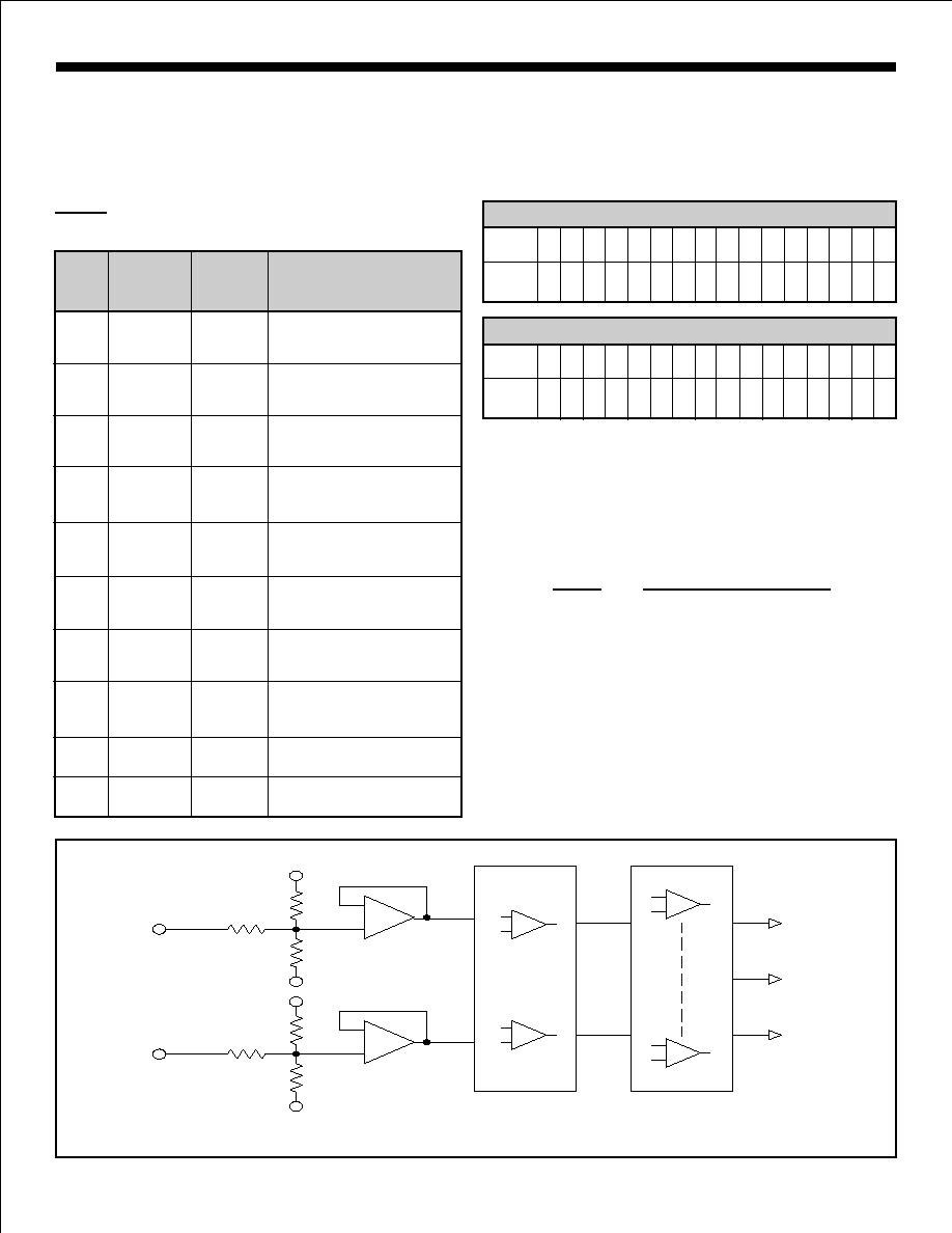
FUNCTIONAL DESCRIPTION
v
cc
v
cc
GND
GND
429DI1 (B)
429DI2 (B)
OR
429DI1 (A)
429DI2 (A)
OR
DIFFERENTIAL
AMPLIFIERS
ONES
COMPARATORS
NULL
ZEROES
FIGURE 1.
ARINC RECEIVER INPUT
CONTROL WORD REGISTER
Both the HI-8581and HI-8589 contain 10 data flip flops whose
D inputs are connected to the data bus and clocks connected to
. Each flip flop provides options to the user as follows:
CWSTR
THE RECEIVERS
ARINC BUS INTERFACE
Figure 1 shows the input circuit for each receiver. The ARINC 429
specification requires the following detection levels:
The HI-8581 and HI-8589 guarantee recognition of these levels with
a common mode Voltage with respect to GND less than ±4V for the
worst case condition (4.75V supply and 13V signal level).
The tolerances in the design guarantee detection of the above
levels, so the actual acceptance ranges are slightly larger. If the
ARINC signal is out of the actual acceptance ranges, including the
nulls, the chip rejects the data.
STATE
DIFFERENTIAL VOLTAGE
ONE
+6.5 Volts to +13 Volts
NULL
+2.5 Volts to -2.5 Volts
ZERO
-6.5 Volts to -13 Volts
HI-8581, HI-8589
HOLT INTEGRATED CIRCUITS
3

RECEIVER LOGIC OPERATION
BIT TIMING
BIT RATE
PULSE RISE TIME
PULSE FALL TIME
PULSE WIDTH
Figure 2 shows a block diagram of the logic section of each receiver.
The ARINC 429 specification contains the following timing specifi-
cation for the received data:
100K BPS ± 1% 12K -14.5K BPS
1.5 ± 0.5 µsec
10 ± 5 µsec
1.5 ± 0.5 µsec
10 ± 5 µsec
5 µsec ± 5%
34.5 to 41.7 µsec
The HI-8581 and HI-8589 accept signals that meet these specifica-
tions and rejects outside the tolerances. The way the logic opera-
tion achieves this is described below:
1. Key to the performance of the timing checking logic is an ac-
curate 1MHz clock source. Less than 0.1% error is recom-
mended.
2. The sampling shift registers are 10 bits long and must show
three consecutive Ones, Zeros or Nulls to be considered valid
data. Additionally, for data bits, the One or Zero in the upper
bits of the sampling shift registers must be followed by a Null in
the lower bits within the data bit time.
For a Null in the word
gap, three consecutive Nulls must be found in both the upper
and lower bits of the sampling shift register. In this manner the
minimum pulse width is guaranteed.
HIGH SPEED
LOW SPEED
FUNCTIONAL DESCRIPTION (cont.)
3. Each data bit must follow its predecessor by not less than
8 samples and no more than 12 samples. In this manner the
bit rate is checked. With exactly 1MHz input clock frequency,
the acceptable data bit rates are as follows:
83K BPS
10.4K BPS
125K BPS
15.6K BPS
4. The Word Gap timer samples the Null shift register every
10 input clocks (80 for low speed) after the last data bit of a
valid reception. If the Null is present, the Word Gap counter
is incremented. A count of 3 will enable the next reception.
The receiver parity circuit counts Ones received, including the par-
ity bit, ARINC bit 32. If the result is odd, then "0" will appear in the
32nd bit.
HIGH SPEED
LOW SPEED
DATA BIT RATE MIN
DATA BIT RATE MAX
RECEIVER PARITY
RETRIEVING DATA
Once 32 valid bits are recognized, the receiver logic generates
an End of Sequence (EOS). If the receiver decoder is enabled
and the 9th and 10th ARINC bits match the control word program
bits or if the receiver decoder is disabled, then EOS clocks the
data ready flag flip flop to a "1",
or
(or both) will go
low. The data flag for a receiver will remain low until after
ARINC bytes from that receiver are retrieved. This is accom-
plished by first activating
with SEL, the byte selector, low to
retrieve the first byte and then activating
with SEL high to re-
trieve the second byte.
retrieves data from receiver 1 and
retrieves data from receiver 2.
If another ARINC word is received and a new EOS occurs before
the two bytes are retrieved, the data is overwritten by the new
word.
D/R1
D/R2
EN
EN
EN1
EN2
both
SEL
EN
D/R
DECODER
CONTROL
BITS
/
MUX
CONTROL
LATCH
ENABLE
CONTROL
32 TO 16 DRIVER
32 BIT LATCH
32 BIT SHIFT REGISTER
TO PINS
CONTROL
BIT BD14
CLOCK
OPTION
CLOCK
CLK
BIT
COUNTER
AND
END OF
SEQUENCE
PARITY
CHECK
32ND
BIT
DATA
BIT CLOCK
EOS
WORD GAP
WORD GAP
TIMER
BIT CLOCK
END
START
SEQUENCE
CONTROL
ERROR
CLOCK
ERROR
DETECTION
SHIFT REGISTER
SHIFT REGISTER
NULL
ZEROS
SHIFT REGISTER
ONES
EOS
BITS 9 & 10
FIGURE 2.
RECEIVER BLOCK DIAGRAM
HI-8581, HI-8589
HOLT INTEGRATED CIRCUITS
4

FUNCTIONAL DESCRIPTION (cont.)
TRANSMITTER
A block diagram of the transmitter section is shown in Figure 3.
The FIFO is loaded sequentially by first pulsing
to load byte 1
and then
to load byte 2. The control logic automatically loads
the 31 bit word in the next available position of the FIFO. If TX/R,
the transmitter ready flag is high (FIFO empty), then 8 words,
each 31 bits long, may be loaded. If TX/R is low, then only the
available positions may be loaded. If all 8 positions are full, the
FIFO ignores further attempts to load data.
When ENTX goes high, enabling transmission, the FIFO
positions are incremented with the top register loading into the
data transmission shift register. Within 2.5 data clocks the first
data bit appears at either TXA(OUT) or TXB(OUT). The 31 bits in
the data transmission shift register are presented sequentially to
the outputs in the ARINC 429 format with the following timing:
ARINC DATA BIT TIME
10 Clocks
80 Clocks
DATA BIT TIME
5 Clocks
40 Clocks
NULL BIT TIME
5 Clocks
40 Clocks
WORD GAP TIME
40 Clocks
320 Clocks
The word counter detects when all loaded positions are
transmitted and sets the transmitter ready flag, TX/R, high.
FIFO OPERATION
DATA TRANSMISSION
PL1
PL2
HIGH SPEED
LOW SPEED
TRANSMITTER PARITY
The parity generator counts the ONES in the 31-bit word. If the
BD12 control word bit is set low, the 32nd bit transmitted will
make parity odd. If the control bit is high, the parity is even.
If the BD05 control word bit is set low, the digital outputs of the
transmitter are internally connected to the logic inputs of the
receivers, bypassing the analog bus interface circuitry. Data to
Receiver 1 is as transmitted and data to Receiver 2 is the
complement. All data transmitted during self test is also present
on the TXA(OUT) and TXB(OUT) line driver outputs.
The two receivers are independent of the transmitter. Therefore,
control of data exchanges is strictly at the option of the user. The
only restrictions are:
1. The received data may be overwritten if not retrieved
within one ARINC word cycle.
2. The FIFO can store 8 words maximum and ignores
attempts to load addition data if full.
3. Byte 1 of the transmitter data must be loaded first.
4. Either byte of the received data may be retrieved first.
Both bytes must be retrieved to clear the data ready flag.
5. After ENTX, transmission enable, goes high it cannot go
low until TX/R, transmitter ready flag, goes high. Otherwise,
one ARINC word is lost during transmission.
SELF TEST
SYSTEM OPERATION
FIGURE 3.
TRANSMITTER BLOCK DIAGRAM
BIT BD12
DATA
CLOCK
CONTROL BIT
BD13
PL1
PL2
CLK
TX CLK
PARITY
GENERATOR
DATA AND
NULL TIMER
SEQUENCER
LINE DRIVER
BIT
AND
WORD GAP
COUNTER
START
SEQUENCE
WORD COUNTER
AND
FIFO CONTROL
INCREMENT
WORD COUNT
DATA CLOCK
DIVIDER
FIFO
LOADING
SEQUENCER
TXA(OUT)
TXB(OUT)
8 X 31 FIFO
31 BIT PARALLEL
LOAD SHIFT REGISTER
BIT CLOCK
WORD CLOCK
ADDRESS
LOAD
DATA BUS
TX/R
ENTX
HI-8581, HI-8589
HOLT INTEGRATED CIRCUITS
5
FUNCTIONAL DESCRIPTION (cont.)
LINE DRIVER OPERATION
The line driver in the HI-8581 and HI-8589 is designed to directly
drive the ARINC 429 bus. The two ARINC outputs (TXA(OUT) and
TXB(OUT)) provide a differential voltage to produce a +10 volt
One, a -10 volt Zero, and a 0 volt Null. Setting Control Register bit
13 to zero causes a slope of 1.5 s on the ARINC outputs. A one in
Control Register bit 13 causes a slope of 10 s. Timing is set by on-
chip resistor and capacitor and tested to be within ARINC require-
ments.
The
HI-8581 has 37.5 ohms whereas the HI-8589 has 10 ohms in
series with each line driver output. The HI-8589 is for applications
where additional external series resistance is required, such as
lightning protection.
m
m
No additional hardware is required to control the slope.
REPEATER OPERATION
Repeater mode of operation allows a data word that has been
received by the HI-8581 or HI-8589 to be placed directly into its
FIFO for transmission.
Repeater operation is similar to normal
receiver operation. In normal operation, either byte of a received
data word may be read from the receiver latches first by use of SEL
input. During repeater operation however, the lower byte of the
data word must be read first. This is necessary because, as the
data is being read, it is also being loaded into the FIFO and the
transmitter FIFO is always loaded with the lower byte of the data
word first.
Signal flow for
repeater operation is shown in the
Timing Diagrams section.
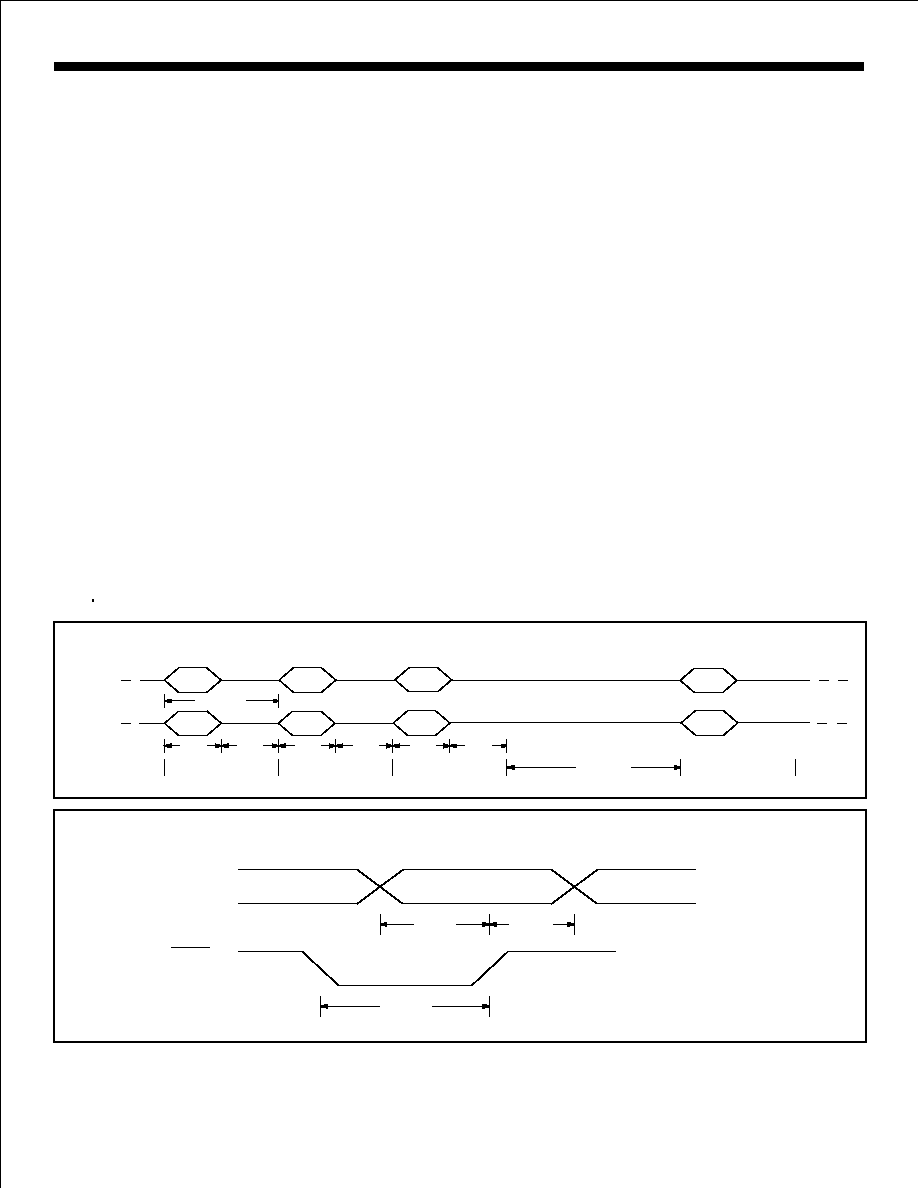
DATA RATE - EXAMPLE PATTERN
TXA(OUT)
ARINC BIT
TXB(OUT)
NULL
DATA
DATA
DATA
NULL
NULL
WORD GAP
BIT 1
NEXT WORD
BIT 32
BIT 31
BIT 30
LOADING CONTROL WORD
CWHLD
t
CWSET
t
CWSTR
t
DATA BUS
CWSTR
VALID
TIMING DIAGRAMS
HI-8581, HI-8589
HI-8581-10 and HI-8589-10
The "-10" versions of the HI-8581 and HI-8589 products require a
10 Kohm resistor to be placed in series with each ARINC input
without affecting the ARINC input
thresholds.
This option is
especially useful in applications where external lightning
protection is required.
Each ARINC input pin must be connected to the ARINC bus
through a 10 Kohm resistor in order for the chip to properly detect
the correct ARINC levels. The typical 10 volt differential signal is
translated and input to a window comparator and latch.
The
comparator levels are set so that with the external 10 Kohm
resistors, they are just below the standard 6.5 volt minimum
ARINC data threshold and just above the 2.5 volt
maximum
ARINC null threshold.
Please refer to the Holt AN-300 Application Note for additional
information and recommendations on lightning protection of Holt
line drivers and line receivers.
POWER SUPPLY SEQUENCING
The power supplies should be controlled to prevent large currents
during supply turn-on and turn-off. The recommended sequence
is V+ followed by Vcc, always ensuring that V+ is the most
positive supply. The V- supply is not critical and can be asserted
at any time.
HOLT INTEGRATED CIRCUITS
6
TIMING DIAGRAMS (cont.)
HI-8581, HI-8589
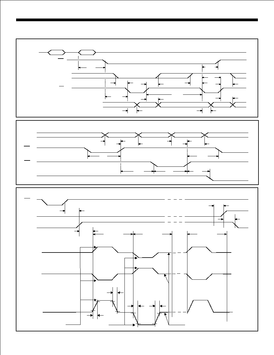
TRANSMITTER OPERATION
PL2
DWSET
t
DWHLD
t
TX/R
t
DWHLD
t
PL12
t
PL
t
DATA BUS
PL1
TX/R
BYTE 2 VALID
PL
t
PL12
t
DWSET
t
BYTE 1 VALID
TRANSMITTING DATA
ARINC BIT
ARINC BIT
PL2
ENTX
TXA(OUT)
TXB(OUT)
DIFF
V
(TXA(OUT) - TXB(OUT))
+5V
+5V
+5V
+10V
+10V
-10V
-5V
-5V
-5V
TX/R
PL2EN
t
ENDAT
t
DTX/R
t
ENTX/R
t
DATA
BIT 1
DATA
BIT 2
DATA
BIT 32
one level
zero level
null level
90%
90%
10%
10%
t
fx
t
rx
t
fx
t
rx
ARINC BIT
RECEIVER OPERATON
DATA READY FLAG
D/R
ARINC DATA
BYTE SELECT
SEL
ENABLE BYTE ON BUS
EN
DATA BUS
BIT 31
BIT 32
SELEN
t
D/R
t
ENSEL
t
DATAEN
t
D/REN
t
END/R
t
EN
t
ENSEL
t
SELEN
t
DATAEN
t
ENDATA
t
ENDATA
t
ENEN
t
DON'T CARE
DON'T CARE
DON'T CARE
BYTE 1 VALID
BYTE 2 VALID
HOLT INTEGRATED CIRCUITS
7

TIMING DIAGRAMS (cont.)
REPEATER OPERATION TIMING
DON'T CARE
429DI
D/R
EN
PL1
PL2
SEL
TX/R
ENTX
TXA(OUT)
TXB(OUT)
BIT 32
DON'T CARE
D/R
t
EN
t
D/REN
t
ENEN
t
EN
t
END/R
t
SELEN
t
ENSEL
t
ENPL
t
PLEN
t
SELEN
t
ENSEL
t
ENPL
t
PLEN
t
TX/R
t
TX/REN
t
ENDAT
t
ENTX/R
t
DTX/R
t
NULL
t
BIT 1
BIT 32
HI-8581, HI-8589
HOLT INTEGRATED CIRCUITS
8

LIMITS
PARAMETER
CONDITIONS
UNIT
SYMBOL
Differential Input Voltage:
ONE
V
Common mode voltage
6.5
10.0
13.0
V
(429DI1(A) to 429DI1(B); 429DI2(A) to 429DI2(B))
ZERO
V
less than ±4V with
-13.0
-10.0
-6.5
V
NULL
V
respect to GND
-2.5
0
2.5
V
Input Resistance:
Differential
R
12
K
To GND
R
12
27
K
To Vcc
R
12
27
K
Input Current:
Input Sink
I
200
µA
Input Source
I
-450
µA
Input Capacitance:
Differential
C
20
pF
To GND
C
20
pF
To Vcc
C
20
pF
Input Voltage:
Input Voltage HI
V
2.1
V
Input Voltage LO
V
0.7
V
Input Current:
Input Sink
I
1.5
µA
Input Source
I
-1.5
µA
Input Voltage:
Input Voltage HI
V
3.5
V
Input Voltage LO
V
0.7
V
Input Current:
Input Sink
I
10
µA
Input Source
I
-20
MIN
TYP
MAX
ARINC INPUTS
BI-DIRECTIONAL INPUTS
OTHER INPUTS
IH
IL
NUL
I
G
H
IH
IL
I
G
H
IH
IL
IH
IL
IH
IL
IH
IL
(Guaranteed but not tested)
(429DI1(A), 429DI1(B), 429DI2(A) & 429DI2(B))
Vcc = 5V ±5%,
GND = 0V, TA = Operating Temperature Range (unless otherwise specified).
V+ = 10V , V- = -10V,
Power Dissipation at 25∞C
Plastic PLCC/PQFP
1.5 W, derate 10mW/ C
Ceramic J-LEAD CERQUAD
1.0 W, derate 7mW/
DC Current Drain per pin
±10mA
Operating Temperature Range:
(Industrial)
-40∞C to +85∞C
(Military)
-55∞C to +125∞C
∞
∞C
Storage Temperature Range:
-65∞C to +150∞C
ABSOLUTE MAXIMUM RATINGS
Supply Voltages Vcc
-0.3V to +7V
V+
+12.5V
V-
-12.5V
Voltage at ARINC inputs
-29V to +29V
Soldering Temperature (Leads)
280∞C for 10 seconds
(Package)
220∞C
Voltage at any other pin
-0.3V to Vcc +0.3V
NOTE: Stresses above those listed under "Absolute Maximum Ratings" may cause permanent damage to the device. These are stress ratings only.
Functional operation of the device at these or any other conditions above those indicated in the operational sections of the specifications is not implied.
Exposure to absolute maximum rating conditions for extended periods may affect device reliability.
DC ELECTRICAL CHARACTERISTICS
HI-8581, HI-8589
HOLT INTEGRATED CIRCUITS
9

LIMITS
PARAMETER
CONDITIONS
UNIT
SYMBOL
Output Voltage:
Logic "1" Output Voltage
V
I
= -1.5mA
2.7
V
Logic "0" Output Voltage
V
I
= 2.6mA
0.4
V
Output Current:
Output Sink
I
V
= 0.4V
3.0
mA
(Bi-directional Pins)
Output Source
I
V
= V
- 0.4V
1.1
mA
Output Current:
Output Sink
I
V
= 0.4V
2.6
mA
(All Other Outputs)
Output Source
I
V
= V
- 0.4V
1.1
mA
Output Capacitance:
C
15
pF
V
4.75
5.25
V
V+
9.5
10.5
V
V-
-9.5
-10.5
V
V
I
20
mA
MIN
TYP
MAX
ARINC OUTPUTS
OTHER OUTPUTS
Operating Voltage Range
Operating Supply Current
OH
OH
OL
OL
OL
OUT
OH
OUT
CC
OL
OUT
OH
OUT
CC
O
CC
CC
CC1
ARINC output voltage
One or zero
V
no load and magnitude at pin
4.50
5.00
5.50
V
Null
V
-0.25
0.25
V
ARINC output current
I
80
mA
V+
I
16
mA
V-
I
16
mA
DOUT
NOUT
"
"
"
"
"
"
OUT
DD1
EE1
Vcc = 5V ±5%, V+ = 10V, V- = -10V, GND = 0V, TA = Operating Temperature Range (unless otherwise specified).
DC ELECTRICAL CHARACTERISTICS
(cont.)
HI-8581, HI-8589
HOLT INTEGRATED CIRCUITS
10

LIMITS
PARAMETER
SYMBOL
UNITS
MIN
TYP
MAX
CONTROL WORD TIMING
RECEIVER TIMING
FIFO TIMING
TRANSMISSION TIMING
LINE DRIVER OUTPUT TIMING
Pulse Width -
t
80
ns
Setup - DATA BUS Valid to
HIGH
t
50
ns
Hold -
HIGH to DATA BUS Hi-Z
t
10
ns
Delay - Start ARINC 32nd Bit to
LOW: High Speed
t
16
µs
Low Speed
t
128
µs
Delay -
LOW to
LOW
t
0
ns
Delay -
LOW to
HIGH
t
200
ns
Setup - SEL to
LOW
t
10
ns
Hold - SEL to
HIGH
t
10
ns
Delay -
LOW to DATA BUS Valid
t
50
100
ns
Delay -
HIGH to DATA BUS Hi-Z
t
30
ns
Pulse Width -
or
t
80
ns
Spacing -
HIGH to next
LOW
t
50
ns
Pulse Width -
or
t
80
ns
Setup - DATA BUS Valid to
HIGH
t
50
ns
Hold -
HIGH to DATA BUS Hi-Z
t
10
ns
Spacing -
or
t
0
ns
Delay -
HIGH to TX/R LOW
t
840
ns
Spacing -
HIGH to ENTX HIGH
t
0
µs
Delay - 32nd ARINC Bit to TX/R HIGH
t
50
ns
Spacing - TX/R HIGH to ENTX LOW
t
0
ns
Line driver transition differential times:
high to low
t
1.0
1.5
2.0
CWSTR
CWSTR
CWSTR
D/R
D/R
EN
EN
D/R
EN
EN
EN
EN
EN1
EN2
EN
EN
PL1
PL2
PL
PL
PL1
PL2
PL2
PL2
CWSTR
CWSET
CWHLD
D/R
D/R
D/REN
END/R
SELEN
ENSEL
ENDATA
DATAEN
EN
ENEN
PL
DWSET
DWHLD
PL12
TX/R
PL2EN
DTX/R
ENTX/R
fx
Delay - ENTX HIGH to TXA(OUT) or TXB(OUT): High Speed
t
25
Delay - ENTX HIGH to TXA(OUT) or TXB(OUT): Low Speed
t
200
low to high
t
1.0
1.5
2.0
ENDAT
ENDAT
rx
µs
µs
(High Speed)
µs
µs
(Low Speed)
high to low
t
5.0
10
15
µs
low to high
t
5.0
10
15
µs
Delay -
LOW to
LOW
t
0
ns
Hold -
HIGH to
HIGH
t
0
ns
Delay - TX/R LOW to ENTX HIGH
t
0
ns
t
400
ns
± 1%
fx
rx
ENPL
PLEN
TX/REN
MR
REPEATER OPERATION TIMING
MASTER RESET PULSE WIDTH
ARINC DATA RATE AND BIT TIMING
EN
PL
PL
EN
AC ELECTRICAL CHARACTERISTICS
Vcc = 5V, V+=10V, V- = -10V, GND = 0V, TA = Oper. Temp. Range and fclk = 1MHz 0.1% with 60/40 duty cycle
+
HI-8581, HI-8589
HOLT INTEGRATED CIRCUITS
11
ADDITIONAL HI-8581 / HI-8589 PIN CONFIGURATIONS
429DI2(B) 7
8
9
SEL 10
11
12
BD15 13
BD14 14
BD13 15
BD12 16
BD11 17
D/R1
D/R2
EN1
EN2
39 ENTX
38 N/C
37 V+
36 TXB(OUT)
35 TXA(OUT)
34 V-
33 GND
32 TX/R
31
30
29 BD00
PL2
PL1
BD10
18
BD09
19
BD08
20
BD07
21
BD06
22
GND
23
BD05
24
BD04
25
BD03
26
BD02
27
BD01
28
6
429DI2(A)
5
429DI1(B)
4
429DI1(A)
3V
C
C
2
N/C
1
44
TXCLK
43
CLK
42
N/C
41
N/C
40
MR
CWSTR
HI-8581PJI / HI-8589PJI
HI-8581PJT / HI-8589PJT
44-Pin Plastic J-Lead PLCC
429DI2(B) 7
8
9
SEL 10
11
12
BD15 13
BD14 14
BD13 15
BD12 16
BD11 17
D/R1
D/R2
EN1
EN2
39 ENTX
38 N/C
37 V+
36 TXB(OUT)
35 TXA(OUT)
34 V-
33 GND
32 TX/R
31
30
29 BD00
PL2
PL1
BD10
18
BD09
19
BD08
20
BD07
21
BD06
22
GND
23
BD05
24
BD04
25
BD03
26
BD02
27
BD01
28
6
429DI2(A)
5
429DI1(B)
4
429DI1(A)
3V
C
C
2N
/
C
1
44
TXCLK
43
CLK
42
N/C
41
N/C
40
MR
CWSTR
HI-8581CJI / HI-8589CJI
HI-8581CJT / HI-8589CJT
44-Pin J-Lead CERQUAD
HI-8581, HI-8589
ORDERING INFORMATION
10 Ohms
27.5 Ohms
37.5 Ohms
0
PACKAGE
DESCRIPTION
TEMPERATURE
RANGE
LEAD
FINISH
SOLDER
SOLDER
44 PIN PLASTIC J LEAD (PLCC)
44 PIN CERQUAD J LEAD
FLOW
BURN
IN
-40∞C TO +85∞C
NO
I
-55∞C TO +125∞C
NO
T
HI - 8581 xx x - xx
INPUT SERIES RESISTANCE
BUILT-IN
REQUIRED EXTERNALLY
PART
NUMBER
25 Kohm
10 Kohm
-10
35 Kohm
0
No dash number
PART
NUMBER
T
I
PART
NUMBER
PJ
CJ
PART
NUMBER
8581
8589
OUTPUT SERIES RESISTANCE
BUILT-IN
REQUIRED EXTERNALLY
SOLDER
44 PIN PLASTIC QUAD FLAT PACK (PQFP)
PQ
(See page 1 for the 44-Pin Plastic Quad Flat Pack (PQFP) pin configuration)
HOLT INTEGRATED CIRCUITS
12
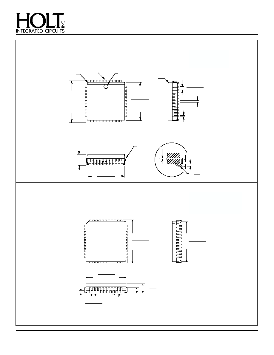
HI-8581, HI-8589 PACKAGE DIMENSIONS
inches (millimeters)
P
T :
ACKAGE YPE
Package Type:
HOLT INTEGRATED CIRCUITS
13
.620 ± .012
(15.748 ± .305)
.688 ± .005
(17.475 ± .127)
MAX.
SQ.
.650 ± .010
(16.510 ± .254)
SQ.
.050
(1.270)
.019 ± .002
(.483 ± .051)
44-PIN CERQUAD J-LEAD
PIN NO. 1 IDENT
.045 x 45∞
.050 ± .005
(1.27 ± .127)
.045 x 45∞
PIN NO. 1
44-PIN PLASTIC J-LEAD PLCC
SEE DETAIL
A
.172 ± .008
(4.369 ± .203)
DETAIL A
.020 MIN
(.508 MIN)
.025
.045
R
.690 ± .005
(17.526 ± .127)
SQ.
.610 ± .020
(15.494± .508)
.031± .005
(.787 ± .127)
.653 ± .004
(16.586 ± .102)
SQ.
.017 ± .004
(.432 ± .102)
.015 ± .002
(.381 ± .051)
.009
.011
.039 ± .005
(.990 ± .127)
TYP.
.100 ± .007
(2.540 ± .178)
.200
(5.080) MAX.
2 1 44 43
HOLT INTEGRATED CIRCUITS
14
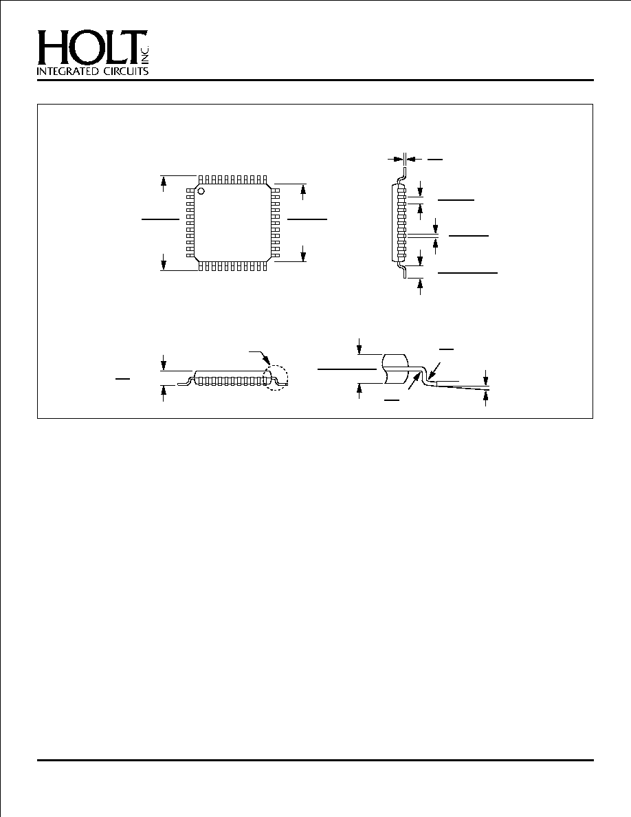
HI-8581, HI-8589 PACKAGE DIMENSIONS
inches (millimeters)
Package Type:
0∞ £ Q £ 7∞
Detail A
See Detail A
SQ.
44PQS
44-PIN PLASTIC QUAD FLAT PACK (PQFP)
.007
(.17)
.547 ± .010
(13.90 ± .25)
.394 ± .004
(10.0 ± .10)
SQ.
MAX.
.014 ± .002
(.35 ± .05)
.035 +.006 / -.004
(.88 +.15 / -.10)
.008
(.20 R)TYP.
.012
(.30 R)TYP.
.079 +.004 / -.006
(2.00 +.10 / -.15)
.097
(2.45) MAX.
.0315 BSC
(.80 BSC)