HI-8783, HI-8784, HI-8785
DESCRIPTION
FEATURES
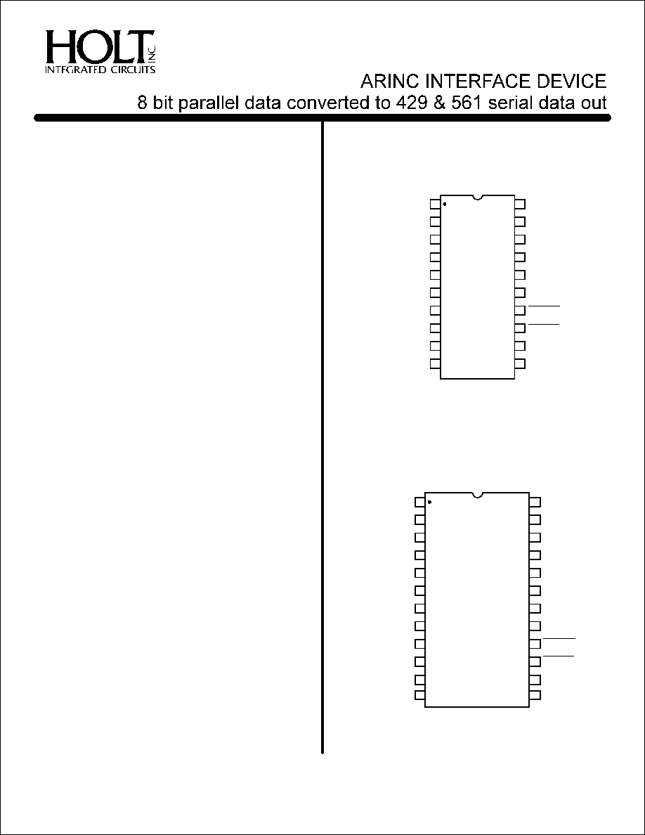
PIN CONFIGURATIONS
The HI-8783, HI-8784, and HI-8785 are system compo-
nents for interfacing 8 bit parallel data to an ARINC 429
bus. The HI-8783 is a logic device only and requires a sep-
arate line driver circuit, such as the HI-8382 or HI-8585.
The HI-8784 and HI-8785 combine logic and line driver on
one chip. The HI-8784 has an output resistance of 37.5
ohms, and the HI-8785 has an output resistance of 10
ohms to facilitate external lightning protection cicuitry. The
technology is analog/digital CMOS.
The HI-8783 is available in a 22 pin DIP format as a second
source replacement for the Micrel / California Devices
DLS-111BV.
The products offer high speed data bus data transactions
to a buffer register. After loading 4 bytes, data is automati-
cally transferred and transmitted. The data rate is equal to
the clock rate. Parity can be enabled in the 32nd bit. Reset
is used to initialize the logic upon startup. Word gaps are
transmitted automatically.
The HI-8784 and HI-8785 require +/- 10 volt supplies in ad-
dition to the 5 volt supply.
Automatically converts 8 bit parallel data
to ARINC 429 or 561 data
High speed data bus interface
On-chip line driver option
SOIC packages available
Military processing options
l
l
l
l
l
(See page 7 for additional pin configurations)
VCC
561 SYNC
D0
D1
D2
D3
D4
D5
D6
D7
561 DATA
DATA ZERO
DATA ONE
PARITY ENB
XMT READY
XMIT CLK
A0
GND
RESET
WRITE
1
2
3
4
5
6
7
8
9
10
20
19
18
17
16
15
14
13
12
11
HI-8783PSI
&
HI-8783PST
20-Pin Plastic SOIC - WB package
V+
561 DATA
TXBOUT
TXAOUT
V-
PARITY ENB
XMT READY
XMIT CLK
SLP1.5
A0
RESET
WRITE
VCC
561 SYNC
D0
D1
D2
D3
D4
D5
D6
NC
D7
GND
1
2
3
4
5
6
7
8
9
10
11
24
23
22
21
20
19
18
17
16
15
14
HI-8784PSI
HI-8784PST
HI-8785PSI
&
HI-8785PST
12
13
24-Pin Plastic SOIC - WB package
(DS8783 Rev. B)
01/01
January 2001
HOLT INTEGRATED CIRCUITS
1
HI-8783, HI-8784, HI-8785
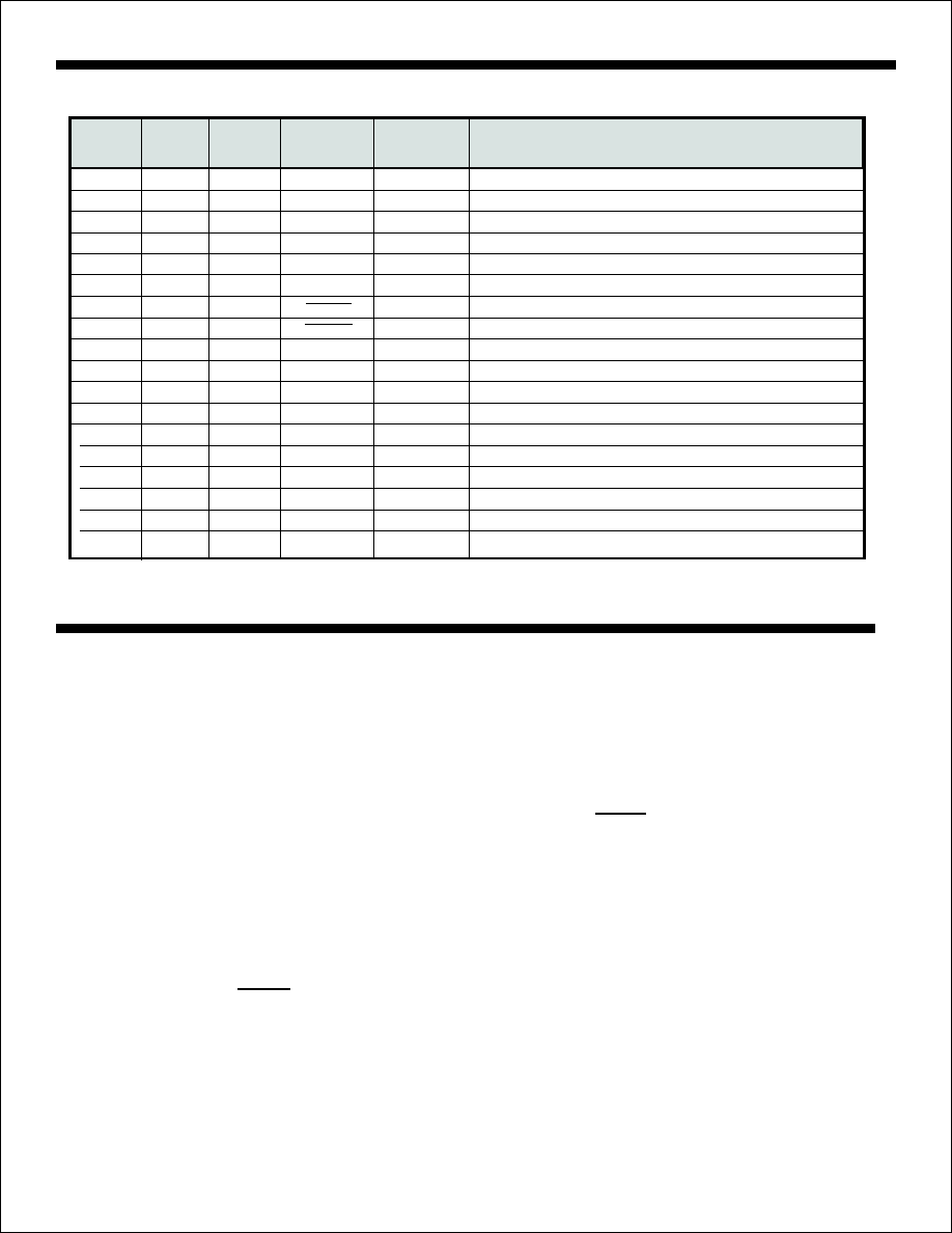
PIN DESCRIPTIONS
The HI-8783 is a parallel to serial converter, which when
loaded with four eight bit parallel bytes, outputs the data as
a 32 bit serial word. Timing circuitry inserts a 4 bit gap at the
end of each 32 bit word. An input buffer register allows load
operations to take place while the previously loaded word
is being transmitted.
If the PARITY ENB pin is high, the 32nd bit will be a parity
bit, inserted so as to make the 32 bit word have odd parity. If
the PARITY ENB pin is low, the 32nd bit will be the D7 bit of
the 4th byte.
Outputs are provided for both ARINC 429/575 (DATA ONE
and DATA ZERO pins), and ARINC 561 (561 DATA and
561 SYNC pins) type data.
A low signal applied to the
pin resets the HI-8783's
internal logic so that spurious transmission does not take
place during power-up. The registers are cleared so that a
continuous gap will be transmitted until the first word is
loaded into the transmitter.
RESET
FUNCTIONAL DESCRIPTION
PIN
PIN
PIN
SYMBOL
FUNCTION
DESCRIPTION
HI-8783 HI-8783
HI-8784
(20-pin) (22-pin)
HI-8785
2
1
2
561 SYNC
digital output
ARINC 561 Sync signal
3-10
2-8,10
3-9,11
Dn
digital inputs
Parallel 8 bit Data Input
11
11
12
GND
power supply Ground
12
12
13
A0
digital input
Byte address, A0=1 for 1st byte, A0=0 for 2nd, 3rd & 4th bytes
-
-
14
SLP1.5
digital input
Selects the slope of the line driver. High = 1.5us
13
14
15
digital input
Write strobe, loads data on rising edge
14
15
16
digital input
Registers and sequencing logic initialized when low
15
16
17
XMIT CLK
digital input
Clock input for the transmitter
16
17
18
XMT RDY
digital output
Goes high if the buffer register is empty
17
18
19
PARITY ENB digital input
When high the 32nd bit output is odd parity
-
-
20
V-
power supply -10 volt rail
18
19
-
DATA ONE
digital output
Goes high for each ARINC bit output that is a "one"
19
20
-
DATA ZERO digital output
Goes high for each ARINC bit output that is a "zero"
-
-
21
TXAOUT
analog output Line driver ouptut - A side
-
-
22
TXBOUT
analog output Line driver output - B side
20
21
23
561 DATA
digital output
Serial output for ARINC 561 data
-
-
24
V+
power supply +10 volt rail
1
22
1
VCC
power supply +5 volt rail,
WRITE
RESET
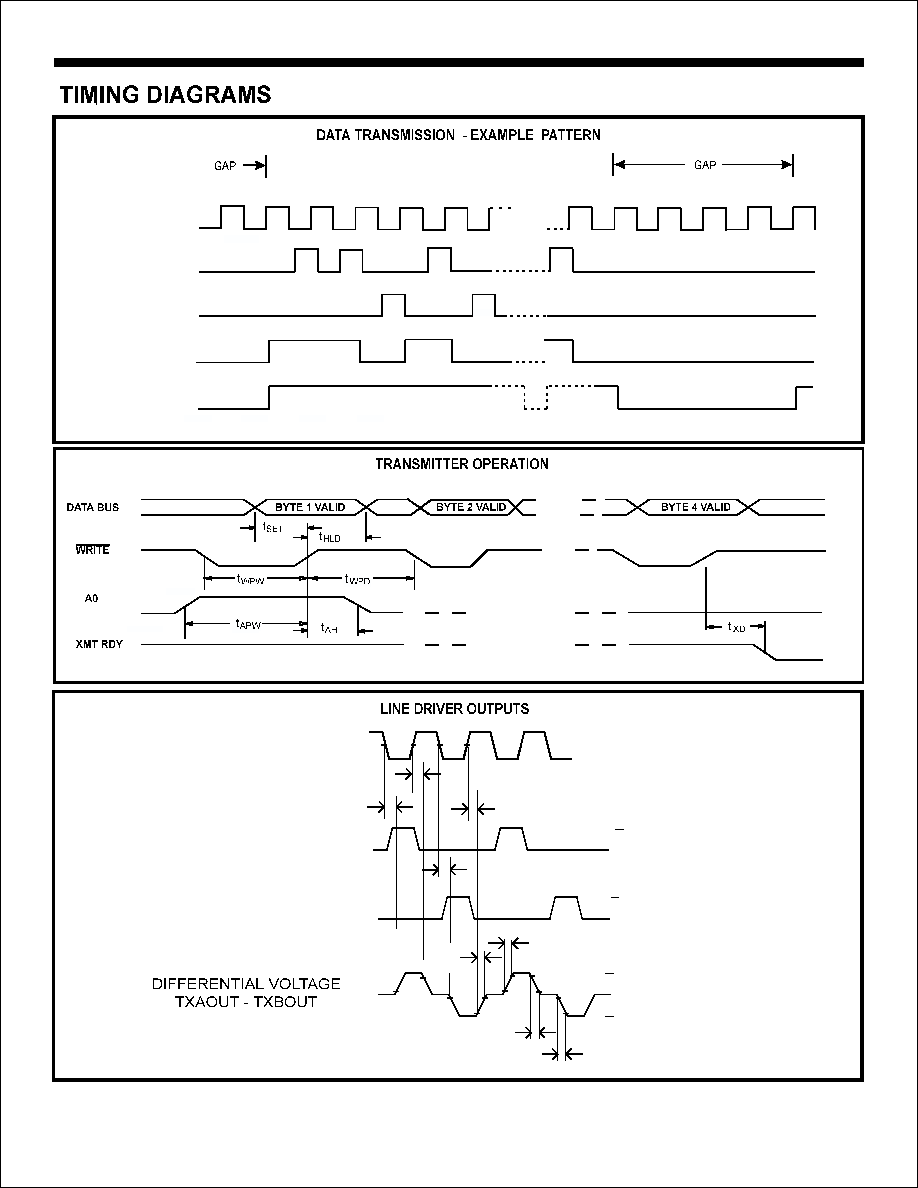
Input data can be loaded when the XMT RDY signal is
high, which indicates the input buffer register is empty. The
first 8 bit byte is the label byte and is loaded with the A0 in-
put high, which initializes the internal byte counter. The re-
maining three bytes are loaded with A0 in the low state.
Each 8 bit byte is loaded into the input buffer register by a
low pulse on the
input. (See figure 1). After the
fourth byte is loaded, the XMT RDY output goes low. The
contents of the input buffer register are transferred to the
output register during the fourth bit period of the gap. If the
fourth gap bit period of the previous word has already been
transmitted, the contents of the input buffer register will be
transferred to the output shift register during the first bit pe-
riod after the loading of the fourth byte, and the XMT RDY
output goes high.
After the output shift register is loaded, the data is shifted
out to the output logic in the order shown in figure 2.
WRITE
The 561 SYNC output pulses low when the XMT CLK is low
during the 8th bit of the ARINC transmission.
The XMIT CLK is the same as the data rate.
HOLT INTEGRATED CIRCUITS
2
HI-8783, HI-8784, HI-8785
The HI-8784 and HI-8785 have the same digital logic func-
tion as the HI-8783, but include an on-chip line driver de-
signed to directly drive the ARINC 429 bus. The two ARINC
outputs (TXAOUT and TXBOUT) provide a differential volt-
age to produce a +10 volt One, a -10 volt Zero, and a 0 volt
Null. The slope of the ARINC outputs is controlled by the
SLP1.5 pin. If SLP1.5 is high, the output rise and fall time is
nominally 1.5us. If SLP1.5 is set low, the rise and fall times
are 10us. DATA ONE and DATA ZERO outputs are not pro-
vided for the HI-8784 and HI-8785.
The HI-8784 has 37.5 ohms in series with each line driver
output. The HI-8785 has 10.0 ohms in series. The HI-8785
is for applications where external series resistance is
needed, typically for lightning protection devices.
FUNCTIONAL DESCRIPTION (Cont.)
A0
Byte
Data Bus
ARINC Bits
1
Byte 1
D0 - D7
ARINC 1 - ARINC 8
0
Byte 2
D0 - D7
ARINC 9 - ARINC 16
0
Byte 3
D0 - D7
ARINC 17 - ARINC 24
0
Byte 4
D0 - D7
ARINC 25 - ARINC 32
Figure 2. Order of transmitted bytes
Figure 1. Block Diagram
DATA
BUS
8 to 32 bit
mux
32 bit
buffer
register
32 bit
shift
register
byte
counter
WRITE
A0
8
32
32
status &
control
logic
XMT RDY
XMIT CLK
word gap
counter
bit
counter
output
logic
line
driver
PARITY ENB
DATA ZERO
DATA ONE
561 DATA
561 SYNC
TXBOUT
TXAOUT
SLP1.5
HI-8784, HI8785
HI-8783
HOLT INTEGRATED CIRCUITS
3
HI-8783, HI-8784, HI-8785
XMIT CLK
35
36
1
2
3
4
5
31
32
33
34
35
36
DATA ONE
DATA ZERO
561 DATA
561 SYNC
LOW DURING CLK 8
5V
0V
5V
0V
phlx
t
phlx
t
plhx
t
plhx
t
DATA ONE
DATA ZERO
0V
10V
-10V
rx
t
10%
90%
t
t
10%
90%
t rx
t
10%
t fx
t
fx
XMT CLK
HOLT INTEGRATED CIRCUITS
4
NOTE:
Stresses above absolute maximum
ratings or outside recommended operating
conditions may cause permanent damage to the
device. These are stress ratings only. Operation at
the limits is not recommended.
Voltages referenced to Ground
Supply voltages
V+.................................................12.5V
V-.................................................-12.5V
DC current per input pin................ +10ma
Power dissipation at 25�
plastic DIL............1.0W, derate 10mW/�C
ceramic DIL..........0.5W, derate 7mW/�C
Solder Temperature ........275�C for 10 sec
Storage Temperature........-65�C to +150�C
VCC.................................................. 7V
ABSOLUTE MAXIMUM RATINGS
RECOMMENDED OPERATING CONDITIONS
Supply Voltages
V+.......................................+10V... �5%
V-........................................ -10V... �5%
Temperature Range
Industrial Screening.........-40�C to +85�C
Hi-Temp Screening........-55�C to +125�C
Military Screening..........-55�C to +125�C
VCC....................................... 5V... �5%
VCC = 5.0V, V
= 0V, T = Operating Temperature Range (unless otherwise specified).
SS
A
PARAMETER
SYMBOL
CONDITION
MIN
TYP
MAX
UNITS
Operating Voltage
V
4.75
5
5.25
V
Min. Input Voltage
(HI)
V
2.0
1.4
V
Max. Input Voltage
(LO)
V
1.4
0.8
V
Min. Input Current
(HI)
I
V
= 4.9V
1
�A
Max. Input Current
(LO)
I
V
= 0.1V
-1
�A
Min. Output Voltage
(HI)
V
I
= -1.6mA
2.7
V
Max. Output Voltage
(LO)
V
I
= 1.6mA
0.4
V
Operating Current Drain
I
f = 100khz
0.8
2.8
mA
Input Capacitance
C
Not tested
20
pF
CC
CC
IH
IL
IH
IH
IL
IL
OH
OUT
IH
OUT
IN
VCC = 5.0V, V
= 0V, V+ = 10V, V- = -10V, T = Operating Temperature Range (unless otherwise specified).
SS
A
Minimum Short Circuit Sink or Source Current
I
momentary magnitude
80
mA
OUT
ZERO
"
-5.55
-5.0
-4.5
V
NULL
"
-0.25
0
0.25
V
ONE
no load, VCC = 5.0V
4.5
5.0
5.5
V
Line Driver Output Levels (Ref. To GND)
Operating Current Drain (V-)
I
no load, f = 100khz
-20
-6
mA
EE
Operating Current Drain (V+)
I
no load, f = 100khz
6
20
mA
DD
Operating Voltage
V-
-9.5
-10
10.5
V
Operating Voltage
V+
9.5
10
10.5
V
PARAMETER
SYMBOL
CONDITION
MIN
TYP
MAX
UNITS
HI-8783, HI-8784, HI-8785
Line Driver Output Levels (Differential)
ONE
no load, VCC = 5.0V
9.0
10.0
11.0
V
NULL
"
-0.5
0
0.5
V
ZERO
"
-11.0
-10.0
-9.0
V
HOLT INTEGRATED CIRCUITS
5