 | –≠–ª–µ–∫—Ç—Ä–æ–Ω–Ω—ã–π –∫–æ–º–ø–æ–Ω–µ–Ω—Ç: H02N60F | –°–∫–∞—á–∞—Ç—å:  PDF PDF  ZIP ZIP |
HI-SINCERITY
MICROELECTRONICS CORP.
Spec. No. : MOS200403
Issued Date : 2004.07.01
Revised Date : 2005.07.14
Page No. : 1/6
H02N60I, H02N60J, H02N60E, H02N60F
HSMC Product Specification
H02N60 Series
N-Channel Power Field Effect Transistor
Description
This high voltage MOSFET uses an advanced termination scheme to
provide enhanced voltage-blocking capability without degratding
performance over time. In addition, this advanced MOSFET is designed to
withstand high energy in avalanche and commutation modes. The new
energy efficient design also offers a drain-to-source diode with a fast
recovery time. Designed for high voltage, high speed switching
applications in power supplies, converters and PWM motor controls,
these devices are particularly well suited for bridge circuits where diode
speed and commutating safe operating areas are critical and offer
additional and saafety margin against unexpected voltage transients.
Features
∑
Robust High Voltage Termination
∑
Avalanc he Energy Specified
∑
Source-to-Drain Diode Recovery Time Comparable to a Discrete Fast
Recovery Diode
∑
Diode is Characterized for Use in Bridge Circuits
∑
I
DSS
and V
DS(on)
Specified at Elevated Temperature
Absolute Maximum Ratings
Symbol
Parameter
Value
Units
I
D
Drain to Current (Continuous)
2
A
I
DM
Drain to Current (Pulsed)
8
A
V
GS
Gate-to-Source Voltage (Continue)
±
20
V
Total Power Dissipation (T
C
=25
o
C)
H02N60I (TO-251) / H02N60J (TO-252)
H02N60E (TO-220AB)
H02N60F (TO-220FP)
50
50
25
W
P
D
Derate above 25
∞
C
H02N60I (TO-251) / H02N60J (TO-252)
H02N60E (TO-220AB)
H02N60F (TO-220FP)
0.4
0.4
0.33
W/
∞
C
T
j
, T
stg
Operating and Storage Temperature Range
-55 to 150
∞
C
E
AS
Single Pulse Drain-to-Source Avalanche Enrgy-Tj=25
∞
C
(V
DD
=100V, V
GS
=10V, I
L
=2A, L=10mH, R
G
=25
)
35
mJ
T
L
Maximum Lead Temperature for Soldering Purposes, 1/8"
from case for 10 seconds
260
∞
C
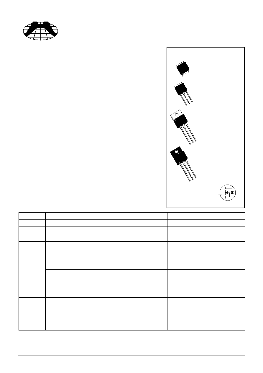
H02N60 Series Pin Assignment
1
2
3
3-Lead Plastic TO-220FP
Package Code: F
Pin 1: Gate
Pin 2: Drain
Pin 3: Source
3-Lead Plastic TO-220AB
Package Code: E
Pin 1: Gate
Pin 2 & Tab: Drain
Pin 3: Source
1
2
3
Tab
3-Lead Plastic TO-252
Package Code: J
Pin 1: Gate
Pin 2 & Tab: Drain
Pin 3: Source
3-Lead Plastic TO-251
Package Code: I
Pin 1: Gate
Pin 2 & Tab: Drain
Pin 3: Source
1
2
3
Tab
1
2
3
Tab
H02N60 Series
Symbol:
G
D
S
HI-SINCERITY
MICROELECTRONICS CORP.
Spec. No. : MOS200403
Issued Date : 2004.07.01
Revised Date : 2005.07.14
Page No. : 2/6
H02N60I, H02N60J, H02N60E, H02N60F
HSMC Product Specification
Thermal Characteristics
Symbol
Parameter
Value
Units
TO-251 / TO-252
2
TO-220AB
2
R
JC
Thermal Resistance Junction to Case Max.
TO-220FP
3.3
∞
C/W
R
JA
Thermal Resistance Junction to Ambient Max.
62.5
∞
C/W
ELectrical Characteristics
(Tj=25
∞
C, unless otherwise specified)
Symbol
Characteristic
Min.
Typ.
Max.
Unit
V
(BR)DSS
Drain-Source Breakdown Voltage (V
GS
=0V, I
D
=250uA)
600
-
-
V
Drain-Source Leakage Current (V
DS
=600V, V
GS
=0V)
-
-
1
uA
I
DSS
Drain-Source Leakage Current (V
DS
=480V, V
GS
=0V, T
j
=125
∞
C)
-
-
50
uA
I
GSSF
Gate-Source Leakage Current-Forward (V
gsf
=20V, V
DS
=0V)
-
-
100
nA
I
GSSR
Gate-Source Leakage Current-Reverse (V
gsr
=-20V, V
DS
=0V)
-
-
-100
nA
V
GS(th)
Gate Threshold Voltage (V
DS
=V
GS
, I
D
=250uA)
2
-
4
V
R
DS(on)
Static Drain-Source On-Resistance (V
GS
=10V, I
D
=1A)*
-
-
4.4
g
FS
Forward Transconductance (V
DS
50V, I
D
=1A)*
1
-
-
mhos
C
iss
Input Capacitance
-
435
-
C
oss
Output Capacitance
-
56
-
C
rss
Reverse Transfer Capacitance
V
GS
=0V, V
DS
=25V, f=1MHz
-
9.2
-
pF
t
d(on)
Turn-on Delay Time
-
12
-
t
r
Rise Time
-
21
-
t
d(off)
Turn-off Delay Time
-
30
-
t
f
Fall Time
(V
DD
=300V, I
D
=2A, R
G
=18
,
V
GS
=10V)*
-
24
-
ns
Q
g
Total Gate Charge
-
13
22
Q
gs
Gate-Source Charge
-
2
-
Q
gd
Gate-Drain Charge
(V
DS
=300V, I
D
=6A, V
GS
=10V)*
-
6
-
nC
L
D
Internal Drain Inductance (Measured from the drain lead 0.25" from
package to center of die)
-
4.5
-
nH
L
S
Internal Drain Inductance (Measured from the drain lead 0.25" from
package to source bond pad)
-
7.5
-
nH
*: Pulse Test: Pulse Width
300us, Duty Cycle
2%
Source-Drain Diode
Symbol
Characteristic
Min.
Typ.
Max.
Units
V
SD
Forward On Voltage(1)
I
S
=2A, V
GS
=0V, T
J
=25
o
C
-
-
1.6
V
t
on
Forward Turn-On Time
-
**
-
ns
t
rr
Reverse Recovery Time
I
S
=2A, V
GS
=0V, d
IS
/d
t
=100A/us
-
340
-
ns
**: Negligible, Dominated by circuit inductance
HI-SINCERITY
MICROELECTRONICS CORP.
Spec. No. : MOS200403
Issued Date : 2004.07.01
Revised Date : 2005.07.14
Page No. : 3/6
H02N60I, H02N60J, H02N60E, H02N60F
HSMC Product Specification
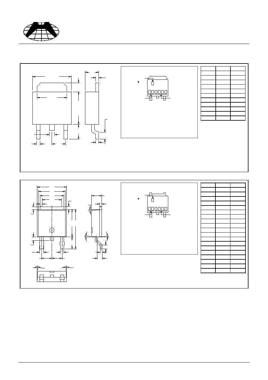
TO-252 Dimension
M
N
A
a2
a5
L
C
3
2
1
a1
G
H
F
a1
A
B
C
D
a1
E
J
K
a2
a2
L
F
G
H
I
y2
y2
a1
M
y1
a1
O
N
y1
y1
3-Lead TO-252 Plastic
Surface Mount Package
HSMC Package Code: J
Marking:
Control Code
Date Code
H
J
0 2
Pb Free Mark
Pb-Free: "
.
"
(Note)
Normal: None
N 6 0
Note: Green label is used for pb-free packing
Pin Style: 1.Gate 2.Drain 3.Source
Material:
∑
Lead solder plating: Sn60/Pb40 (Normal),
Sn/3.0Ag/0.5Cu or Pure-Tin (Pb-free)
∑
Mold Compound: Epoxy resin family,
flammability solid burning class: UL94V-0
DIM
Min.
Max.
A
6.35
6.80
C
4.80
5.50
F
1.30
1.70
G
5.40
6.25
H
2.20
3.00
L
0.40
0.90
M
2.20
2.40
N
0.90
1.50
a1
0.40
0.65
a2
-
*2.30
a5
0.65
1.05
*: Typical, Unit: mm
Marking:
H
J
0 2
Pb Free Mark
Pb-Free: "
.
"
(Note)
Normal: None
N
Control Code
Date Code
6 0
Note: Green label is used for pb-free packing
Pin Style: 1.Gate 2.Drain 3.Source
Material:
∑
Lead solder plating: Sn60/Pb40 (Normal),
Sn/3.0Ag/0.5Cu or Pure-Tin (Pb-free)
∑
Mold Compound: Epoxy resin family,
flammability solid burning class: UL94V-0
3-Lead TO-252 Plastic
Surface Mount Package
HSMC Package Code: J
DIM
Min.
Max.
A
6.40
6.80
B
-
6.00
C
5.04
5.64
D
-
*4.34
E
0.40
0.80
F
0.50
0.90
G
5.90
6.30
H
2.50
2.90
I
9.20
9.80
J
0.60
1.00
K
-
0.96
L
0.66
0.86
M
2.20
2.40
N
0.70
1.10
O
0.82
1.22
a1
0.40
0.60
a2
2.10
2.50
y1
-
5
o
y2
-
3
o
*: Typical, Unit: mm
HI-SINCERITY
MICROELECTRONICS CORP.
Spec. No. : MOS200403
Issued Date : 2004.07.01
Revised Date : 2005.07.14
Page No. : 4/6
H02N60I, H02N60J, H02N60E, H02N60F
HSMC Product Specification
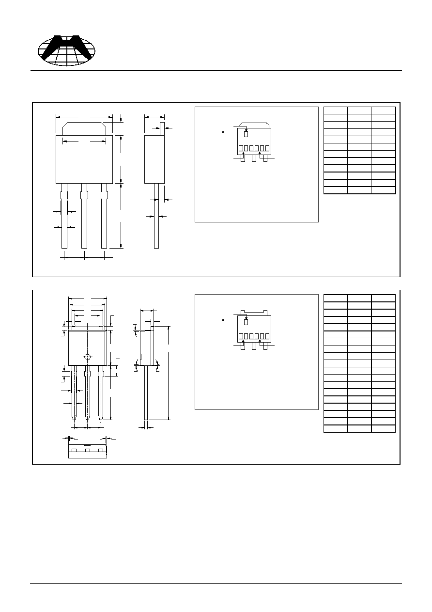
TO-251 Dimension
a1
A
F
G
a2
K1
K
3
2
1
C
a1
M
L
Tab
H1
a2
A
B
C
D
E
a1
F
G
H
H1
K
J
a2
a2
K1
y2
y2
M
a1
y1
a1
y1
y1
I
Marking:
Control Code
Date Code
H
I
0 2
Pb Free Mark
Pb-Free: "
.
"
(Note)
Normal: None
N 6 0
Note: Green label is used for pb-free packing
Pin Style: 1.Gate 2.Drain 3.Source
Material:
∑
Lead solder plating: Sn60/Pb40 (Normal),
Sn/3.0Ag/0.5Cu or Pure-Tin (Pb-free)
∑
Mold Compound: Epoxy resin family,
flammability solid burning class: UL94V-0
3-Lead TO-251
Plastic Package
HSMC Package Code: I
DIM
Min.
Max.
A
6.35
6.80
C
4.80
5.50
F
1.30
1.70
G
5.40
6.25
H1
6.75
8.00
K
0.50
0.90
K1
0.40
0.90
L
0.90
1.50
M
2.20
2.40
a1
0.40
0.65
a2
-
*2.30
*: Typical, Unit: mm
3-Lead TO-251
Plastic Package
HSMC Package Code: I
Marking:
Control Code
Date Code
H
I
0 2
Pb Free Mark
Pb-Free: "
.
"
(Note)
Normal: None
N 6 0
Note: Green label is used for pb-free packing
Pin Style: 1.Gate 2.Drain 3.Source
Material:
∑
Lead solder plating: Sn60/Pb40 (Normal),
Sn/3.0Ag/0.5Cu or Pure-Tin (Pb-free)
∑
Mold Compound: Epoxy resin family,
flammability solid burning class: UL94V-0
DIM
Min.
Max.
A
6.40
6.80
B
-
6.00
C
5.04
5.64
D
-
*4.34
E
0.40
0.80
F
0.50
0.90
G
5.90
6.30
H
-
*1.80
H1
-
*9.30
I
-
*16.10
J
-
*0.80
K
-
0.96
K1
-
*0.76
M
2.20
2.40
a1
0.40
0.60
a2
2.10
2.50
y1
-
5
o
y2
-
3
o
*: Typical, Unit: mm
HI-SINCERITY
MICROELECTRONICS CORP.
Spec. No. : MOS200403
Issued Date : 2004.07.01
Revised Date : 2005.07.14
Page No. : 5/6
H02N60I, H02N60J, H02N60E, H02N60F
HSMC Product Specification
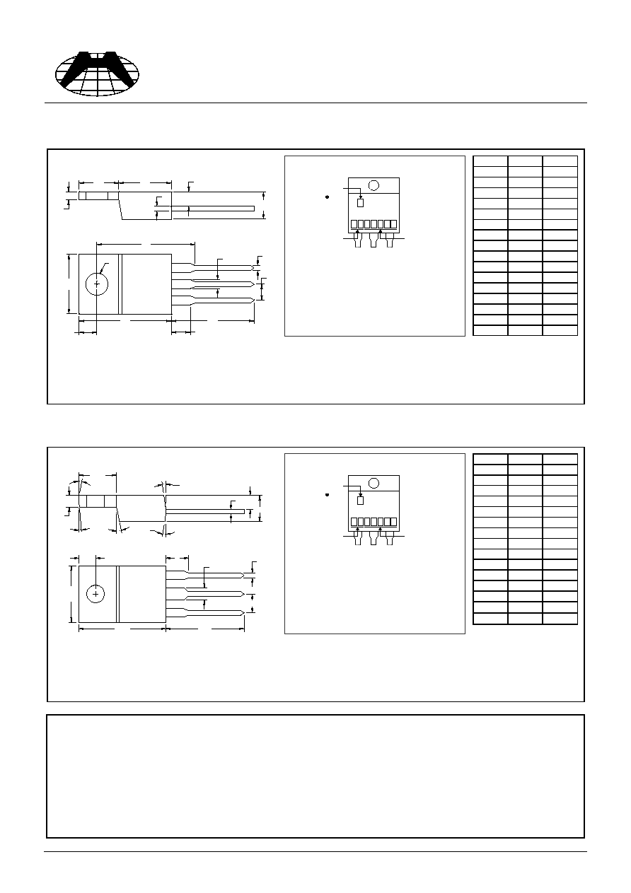
TO-220AB Dimension
TO-220FP Dimension
Important Notice:
∑
All rights are reserved. Reproduction in whole or in part is prohibited without the prior written approval of HSMC.
∑
HSMC reserves the right to make changes to its products without notice.
∑
HSMC semiconductor products are not warranted to be suitable for use in Life-Support Applications, or systems.
∑
HSMC assumes no liability for any consequence of customer product design, infringement of patents, or application assistance.
Head Office And Factory:
∑
Head Office (Hi-Sincerity Microelectronics Corp.): 10F.,No. 61, Sec. 2, Chung-Shan N. Rd. Taipei Taiwan R.O.C.
Tel: 886-2-25212056 Fax: 886-2-25632712, 25368454
∑
Factory 1: No. 38, Kuang Fu S. Rd., Fu-Kou Hsin-Chu Industrial Park Hsin-Chu Taiwan. R.O.C
Tel: 886-3-5983621~5 Fax: 886-3-5982931
A
B
E
G
I
K
M
O
P
3
2
1
C
N
H
D
Tab
F
J
L
Marking:
Control Code
Date Code
H
E
0 2
Pb Free Mark
Pb-Free: "
.
"
(Note)
Normal: None
N 6 0
Note: Green label is used for pb-free packing
Pin Style: 1.Gate 2 & Tab.Drain 3.Source
Material:
∑
Lead solder plating: Sn60/Pb40 (Normal),
Sn/3.0Ag/0.5Cu or Pure-Tin (Pb-free)
∑
Mold Compound: Epoxy resin family,
flammability solid burning class: UL94V-0
3-Lead TO-220AB
Plastic Package
HSMC Package Code: E
DIM
Min.
Max.
A
5.58
7.49
B
8.38
8.90
C
4.40
4.70
D
1.15
1.39
E
0.35
0.60
F
2.03
2.92
G
9.66
10.28
H
-
*16.25
I
-
*3.83
J
3.00
4.00
K
0.75
0.95
L
2.54
3.42
M
1.14
1.40
N
-
*2.54
O
12.70
14.27
P
14.48
15.87
*: Typical, Unit: mm
Marking:
Control Code
Date Code
H
F
0 2
Pb Free Mark
Pb-Free: "
.
"
(Note)
Normal: None
N 6 0
Note: Green label is used for pb-free packing
Pin Style: 1.Gate 2.Drain 3.Source
Material:
∑
Lead solder plating: Sn60/Pb40 (Normal),
Sn/3.0Ag/0.5Cu or Pure-Tin (Pb-free)
∑
Mold Compound: Epoxy resin family,
flammability solid burning class: UL94V-0
3-Lead TO-220FP
Plastic Package
HSMC Package Code: F
A
D
F
G
I
K
L
M
3
2
1
C
J
N
3
E
2
O
4
5
1
DIM
Min.
Max.
A
6.48
7.40
C
4.40
4.90
D
2.34
3.00
E
0.45
0.80
F
9.80
10.36
G
3.10
3.60
I
2.70
3.43
J
0.60
1.00
K
2.34
2.74
L
12.48
13.60
M
15.67
16.20
N
0.90
1.47
O
2.00
2.96
1/2/4/5
-
*5
o
3
-
*27
o
*: Typical, Unit: mm