 | –≠–ª–µ–∫—Ç—Ä–æ–Ω–Ω—ã–π –∫–æ–º–ø–æ–Ω–µ–Ω—Ç: H1563P | –°–∫–∞—á–∞—Ç—å:  PDF PDF  ZIP ZIP |

HI-SINCERITY
MICROELECTRONICS CORP.
Spec. No. : HP200201
HS200207
Issued Date : 2000.10.01
Revised Date : 2002.07.12
Page No. : 1/8
H1563P / H1563S
HSMC Product Specification
H1563P / H1563S
HIGH-EFFICIENCY DC/DC CONVERTER
Description
The H1563 is a monolithic control circuit containing the primary functions required for DC to DC converters
and highside-sensed constant current source. The device consists of an internal temperature compensa-
ted reference, comparator, controlled duty cycle oscillator with an active current sense circuit, bootstrap-
ped driver, and high current output switch. This device is specifically designed to construct a constant
current source for battery chargers with a minimum number of external components. Bootstrapped driver
can drive the NPN output switch to saturation for higher eff-iciency and less heat dissipation. The H1563
can deliver 1.5A continuous current without requiring a heat sink.
Features
∑
3V to 40V Input Voltage Operation
∑
Internal 2A Peak Current Switch
∑
1.5A Continuous Output Current
∑
Bootstrapped Driver
∑
High Side Current Sense Capability
∑
High Efficiency (up to 90%)
∑
Internal ±2% Reference
∑
Low Quiescent Current at 1.6mA
∑
Frequency Operation from 100Hz to 100KHz
Applications
∑
Constant Current Source for Battery Chargers
∑
Saver for Cellular Phone
∑
Step-Down DC-DC Converter Module
Typical Application Circuit
Saver Circuit for Cellular Phone
SC
BST
SE
IS
TC
VCC
GND
FB
R2
120
D2
H1N4148
C3
1uF
L
220uH
Co
220uF
R1
1K
*RS
C5
10uF
RB
33K
RA
5.6K
CT
470pF
C1
220uF
+
Vin
D1
H1N5821
D3
H1N5819
+
+
Io
H1563
*Io=300mV/RS
HI-SINCERITY
MICROELECTRONICS CORP.
Spec. No. : HP200201
HS200207
Issued Date : 2000.10.01
Revised Date : 2002.07.12
Page No. : 2/8
H1563P / H1563S
HSMC Product Specification
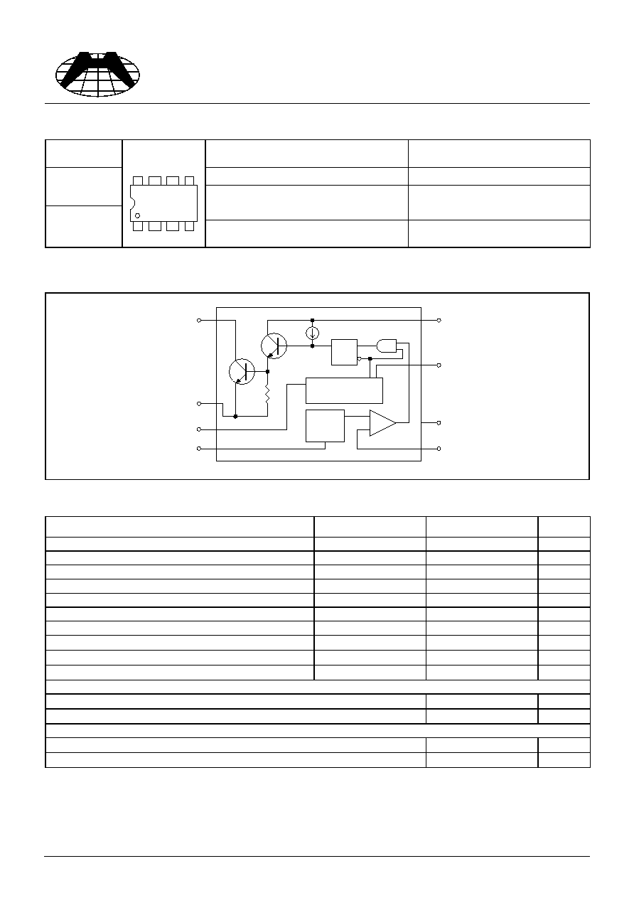
Pin Connections
Order No.
Pin1: SC-2A Switch Collector
Pin5: FB-Feedback Comparator
Inverting Input
Pin2: SE-Darlington Switch Emitter
Pin6: VCC-Power Supply Input
H1563P
(Plastic DIP)
Pin3: TC-Oscillator Timing Capacitor
Pin7: IS-Highside Current Sense
Input
H1563S
(Plastic SO)
Top View
5
6
7
8
4
3
2
1
Pin4: GND-Power Ground
Pin8: BST-Bootstrapped Driver
Collector
Block Diagram
Absolute Maxium Rating
Rating
Symbol
Value
Unit
Power Supply Voltage
Vcc
40
Vdc
Comparator Input Voltage Range
Vir
0.3 ~ +40
Vdc
Switch Collector Voltage
Vc(switch)
40
Vdc
Switch Emitter Voltage (Vpin1=40V)
Ve(switch)
40
Vdc
Switch Collector to Emitter Voltage
Vce(switch)
40
Vdc
Driver Collector Voltage
Vc(driver)
40
Vdc
Switch Current
Isw
2
A
Operating Junction Temperature
Tj
150
∞
C
Operating Ambient Temperature Range
Ta
0 to +70
∞
C
Storage Temperature Range
Tstg
-65 to +150
∞
C
DIP Package Power Dissipation and Thermal Characteristics:
Ta=25
∞
C
1.5
W
Thermal Resistance
85
∞
C/W
SO Package Power Dissipation and Thermal Characteristics:
Ta=25
∞
C
1.2
W
Thermal Resistance
105
∞
C/W
Q2
Q1
80
1.25V
Reference
Voltage
+
-
S
R
-
Q
BST
IS
VCC
FB
GND
SE
TC
SC
CT
Is
Oscillator
5
6
7
8
1
2
3
4
Comparator

HI-SINCERITY
MICROELECTRONICS CORP.
Spec. No. : HP200201
HS200207
Issued Date : 2000.10.01
Revised Date : 2002.07.12
Page No. : 3/8
H1563P / H1563S
HSMC Product Specification
Test Circuit
Characteristics Curve
Vfb Theshold Voltage vs Temperature
1.2
1.22
1.24
1.26
1.28
1.3
0
10
20
30
40
50
60
70
80
Temperature (J)
V
f
b T
h
r
e
s
h
ol
d V
o
l
t
ag
e
(
V
)
VCC=5V
Ct=1nF
PIN2=GND
Standby Supply Current vs Supply Voltage
0
0.4
0.8
1.2
1.6
2
0
5
10
15
20
25
30
35
40
Vcc Supply Voltage (V)
I
c
c
Su
p
p
l
y
C
u
r
r
e
n
t
(
m
A)
Common Emitter Configuration Output Switch
Saturation Voltage vs Collector Current
0
0.2
0.4
0.6
0.8
1
0
0.5
1
1.5
2
Ic Collector Current (A)
V
c
e
(
s
a
t)
S
a
tu
r
a
ti
o
n
V
o
l
t
a
g
e
(
V
)
VCC=5V
PIN7=VCC
PIN2,3,5=GND
Forced Beta=20
Emmiter Follower Configuration Output Switch
Saturtion Voltage vs Emmiter Current
1.2
1.3
1.4
1.5
1.6
1.7
1.8
0
0.5
1
1.5
2
Ie Emitter (A)
V
c
e
(
s
a
t
)
Sa
r
u
r
t
i
o
n
Vo
l
t
a
g
e
(
V
)
VCC=5V
PIN1,7,8=VCC
PIN3,5=GND
SC
BST
SE
IS
TC
VCC
GND
FB
R1
1K
CT
1nF
1A
H1563
5
6
7
8
4
3
2
1
Current Source
2V/0V
I
DISCHG
/I
CHG
VCC
20mA
Current Source
4.55V
@VCC=5V
4.75V
VCC
1.275V
1.225V

HI-SINCERITY
MICROELECTRONICS CORP.
Spec. No. : HP200201
HS200207
Issued Date : 2000.10.01
Revised Date : 2002.07.12
Page No. : 4/8
H1563P / H1563S
HSMC Product Specification
Electrical Characteristics
(Vcc=5V, Ta=25
∞
C, unless otherwise specified)
Parameter
Test Condition
Symbol
Min.
Typ. Max. Unit
Oscillator
Charging Current
5V
V
CC
40V
I
chg
24
35
42
uA
Discharge Current
5V
V
CC
40V
I
dischg
140
220
260
uA
Voltage Swing
Pin3
V
OSC
-
0.6
-
V
Discharge to Charge Current Ratio
V
IS
=V
CC
I
Dischg
/I
chg
-
6
-
Current Limit Sense Voltage
I
Chg
=I
dischg
V
CC
-V
IS
250
300
350
mV
Output Switch
Saturation Voltage, Emitter
Follower Connection
I
SE
=1A, V
BST
=V
SC
=V
CC
V
CE(Sat)
-
1
1.3
V
Saturation Voltage
I
SC
=1A, I
BST
=50mA
(Forced
20)
V
CE(Sat)
-
0.4
0.7
V
DC Current Gain
I
SC
=1A, V
CE
=5V
hFE
35
120
-
Collector Off-State Current
V
CE
=30V
I
CC(Off)
-
10
-
nA
Comparator
Ta=25
∞
C
1.227 1.25 1.273
V
Threshold Voltage
0
∞
C
Ta
70
∞
C
V
FB
1.21
-
1.29
V
Threshold Voltage Line Regulation
3V
V
CC
40V
REG
Line
-
3
6
mV
Input Bias Current
V
IN
=0V
I
IB
-
20
400
nA
Supply Current
V
IS
=V
CC
, V
Pin5
>
V
FB
5V
V
CC
40V, C
T
=1nF
Pin2=Gnd
Remaining pins open
I
CC
-
1.6
3
mA
Application Information
Design Formula Table
Calculation
Step-Down
Step-Up
t
on
/ t
off
V
out
+V
F
/ (V
in(min)
-V
sat
-V
out
)
Vout+V
F
-V
in(min)
/ (V
in(min)
-V
sat
)
(t
on
+t
off
) max
1 / F
min
1 / F
min
C
T
4*10
-5
t
on
4*10
-5
t
on
I
C(switch)
2*I
out(max)
2*I
out(max)*
(t
on
+t
off
/ t
off
)
RS
0.3 / I
C(switch)
0.3 / I
C(switch)
L
(min)
((V
in(min)-
V
sat
-V
out
) /
I
C(switch)
)*t
on(max)
((V
in(min)-
V
sat
)
/
I
C(switch)
)*t
on(max)
C
O
I
C(switch)
*(t
on
+t
off)
/ 8V
Ripple(P-P)
I
out
*t
on
/ V
Ripple(P-P)
V
sat
: Saturation voltage of the output switch.
V
F
: Forward voltage of the ringback rectifier.
The following power supply characteristics must be chosen:
V
in
: Nominal input voltage.
V
out
: Desired output voltage. |V
out
|=1.25*(1+RB/RA)
I
out
: Desired output current
Fmin: Minimum desired switching frequency at selected values for V
in
and I
out
.
V
Ripple(P-P)
: Desired peak to peak output ripple voltage in practice, the calculated value will need to be increased due
to the capacitor equivalent series resistance and board layout. The ripple voltage should be kept to a low
value since it will directly effect the line and load regulation.

HI-SINCERITY
MICROELECTRONICS CORP.
Spec. No. : HP200201
HS200207
Issued Date : 2000.10.01
Revised Date : 2002.07.12
Page No. : 5/8
H1563P / H1563S
HSMC Product Specification
Application Information
(Continuos)
SC
BST
SE
IS
TC
VCC
GND
FB
D2
H1N4148
L1
300uH
C4
470uF
RB
13K
C2
470pF
C3
1uF
+
Vin
D1
H1N5819
+
H1563
RS
0.22
C1
100uF
16V~25V
1
2
3
4
5
6
7
8
+
RA
1.5K
12V/1A
5V
SC
BST
SE
IS
TC
VCC
GND
FB
R1
470
D2
H1N4148
L1
300uH
C4
470uF
R2
390K
RB
3K
C2
1000pF
C3
1uF
+
Vin
D1
H1N5819
+
H1563
D3
1N1418
R3
2.2M
RS
0.22
C1
100uF
8V~25V
1
2
3
4
5
6
7
8
+
RA
1K
5V/1A
SC
BST
SE
IS
TC
VCC
GND
FB
L
200uH
Co
220uF
RB
47K
CT
680pF
+
Vin
D1
H1N5819
+
H1563
RS
0.22
C1
100uF
1
2
3
4
5
6
7
8
RA
2.2K
28V/200mA
R1
150
Vout
Line Regulation: 40mV (Vin=10V~20V, @Io=1A)
Load Regulation: 20mV (Vin=15V, @Io=100mA~1A)
Short Circuit Current: 1.3A (Vin=15V, @RL=0.1
)
Fig.1 Step-Down Converter
Fig.2 Step-Down Converter With External 5V Bootstrap
Fig.3 Step-Up Converter
Line Regulation: 100mV (Vin=8V~16V, @Io=200mA)
Load Regulation: 40mV (Vin=12V, @Io=80mA~200mA)