HI-SINCERITY
MICROELECTRONICS CORP.
Spec. No. : HE6274-B
Issued Date : 1994.11.18
Revised Date : 2000.09.28
Page No. : 1/3
HSMC Product Specification
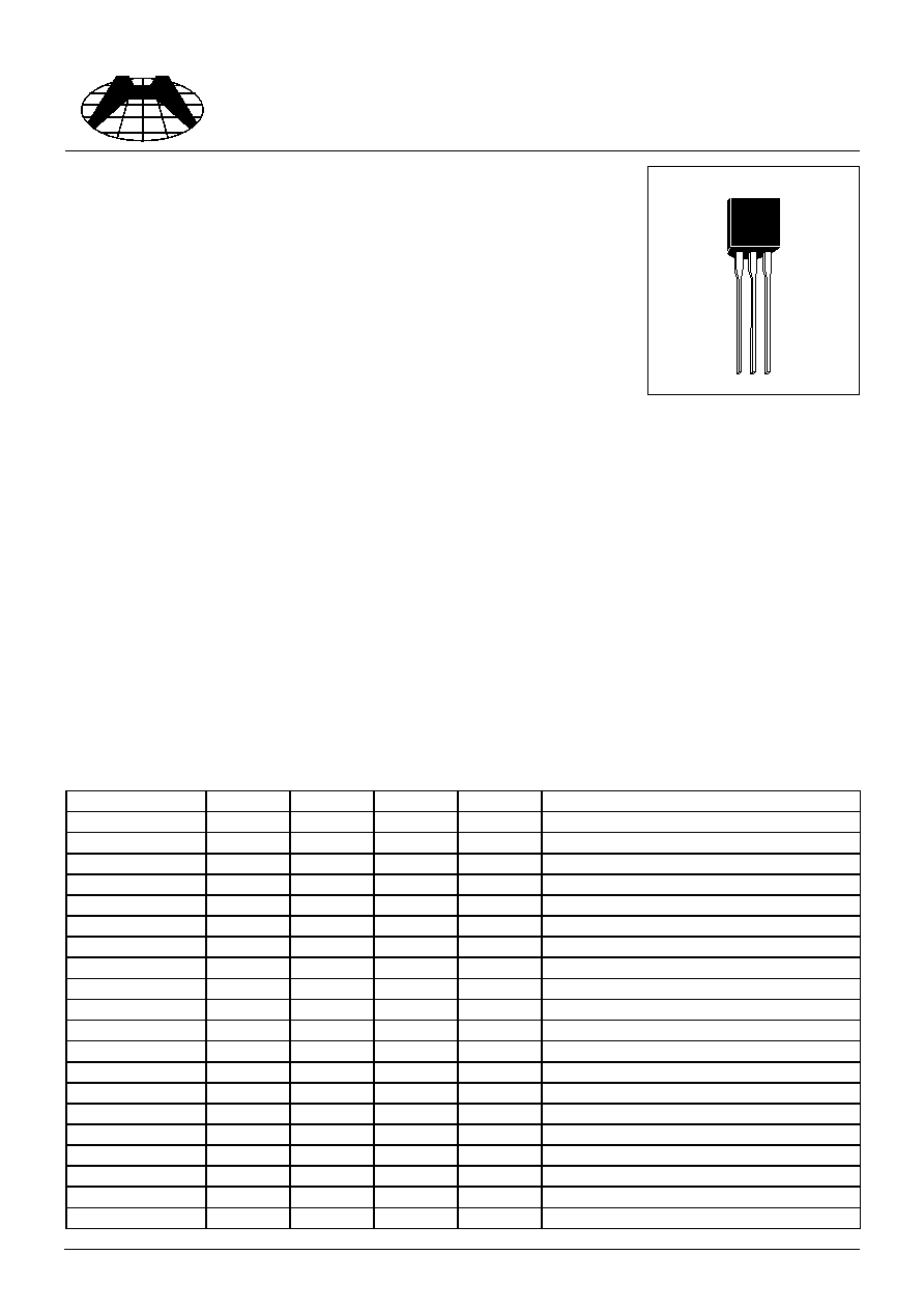
H2N6520
PNP EPITAXIAL PLANAR TRANSISTOR
Description
The H2N6520 is designed for general purpose applications requiring high
breakdown voltages.
Features
∑
High Collector-Emitter Breakdown Voltage
∑
Low Collector-Emitter Saturation Voltage
∑
The H2N6520 is complementary to H2N6517
Absolute Maximum Ratings
∑
Maximum Temperatures
Storage Temperature ....................................................................................................... -55 ~ +150
∞
C
Junction Temperature ............................................................................................... +150
∞
C Maximum
∑
Maximum Power Dissipation
Total Power Dissipation (Ta=25
∞
C)............................................................................................ 625 mW
∑
Maximum Voltages and Currents (Ta=25
∞
C)
VCBO Collector to Base Voltage.................................................................................................. -350 V
VCEO Collector to Emitter Voltage............................................................................................... -350 V
VEBO Emitter to Base Voltage......................................................................................................... -5 V
IC Collector Current ................................................................................................................. -500 mA
IB Base Current ....................................................................................................................... -250 mA
Characteristics
(Ta=25
∞
C,
*Pulse Test : Pulse Width
380us, Duty Cycle
2%
)
Symbol
Min.
Typ.
Max.
Unit
Test Conditions
BVCBO
-350
-
-
V
IC=-100uA, IE=0
BVCEO
-350
-
-
V
IC=-1mA, IB=0
BVEBO
-5
-
-
V
IE=-10uA, IC=0
ICBO
-
-
-50
nA
VCB=-250V, IE=0
IEBO
-
-
-50
nA
VEB=-4V, IC=0
*VCE(sat)1
-
-
-0.30
V
IC=-10mA, IB=-1mA
*VCE(sat)2
-
-
-0.35
V
IC=-20mA, IB=-2mA
*VCE(sat)3
-
-
-0.50
V
IC=-30mA, IB=-3mA
*VCE(sat)4
-
-
-1
V
IC=-50mA, IB=-5mA
VBE(on)
-
-
2
V
IC=-100mA, VCE=-10V
*VBE(sat)1
-
-
-0.75
V
IC=-10mA, IB=-1mA
*VBE(sat)2
-
-
-0.85
V
IC=-20mA, IB=-2mA
*VBE(sat)3
-
-
-0.90
V
IC=-30mA, IB=-3mA
*hFE1
20
-
-
VCE=-10V, IC=-1mA
*hFE2
30
-
-
VCE=-10V, IC=-10mA
*hFE3
30
-
200
VCE=-10V, IC=-30mA
*hFE4
20
-
200
VCE=-10V, IC=-50mA
*hFE5
15
-
-
VCE=-10V, IC=-100mA
fT
40
-
200
MHz
IC=-10mA, VCE=-20V, f=20MHz
Cob
-
-
6
pF
VCB=-20V, f=1MHz, IE=0

HI-SINCERITY
MICROELECTRONICS CORP.
Spec. No. : HE6274-B
Issued Date : 1994.11.18
Revised Date : 2000.09.28
Page No. : 2/3
HSMC Product Specification
Characteristics Curve
Current Gain & Collector Current
1
10
100
0.01
0.1
1
10
100
1000
Collector Current (mA)
hF
E
V
CE
=10V
Saturation Voltage & Collector Current
1
10
100
1000
10000
100000
0.001
0.01
0.1
1
10
100
1000
Collector Current (mA)
S
a
tu
r
a
ti
o
n
V
o
l
t
a
g
e
(
m
V
)
V
BE(sat)
@ I
C
=10I
B
V
CE(sat)
@ I
C
=10I
B
On Voltage & Collector CurrentT
100
1000
10000
0.01
0.1
1
10
100
1000
Collector Current (mA)
On
V
o
l
t
a
g
e
(
m
V
)
V
BE(ON)
@ V
CE
=10V
Cutoff Frequency & Collector Current
10
100
1
10
100
Collector Current (mA)
C
u
to
ff F
r
e
q
u
e
n
c
y
V
CE
=20V
Capacitance & Reverse-Biased Voltage
1
10
100
0.1
1
10
100
Reverse-Biased Voltage (V)
C
a
pa
c
i
t
a
n
c
e (
p
F
)
Cob
PD-Ta
0
100
200
300
400
500
600
700
0
20
40
60
80
100
120
140
160
Ambient Temperature-Ta(
o
C)
P
o
w
e
r D
i
s
s
i
p
a
t
i
o
n
-P
D
(
m
W
)
HI-SINCERITY
MICROELECTRONICS CORP.
Spec. No. : HE6274-B
Issued Date : 1994.11.18
Revised Date : 2000.09.28
Page No. : 3/3
HSMC Product Specification
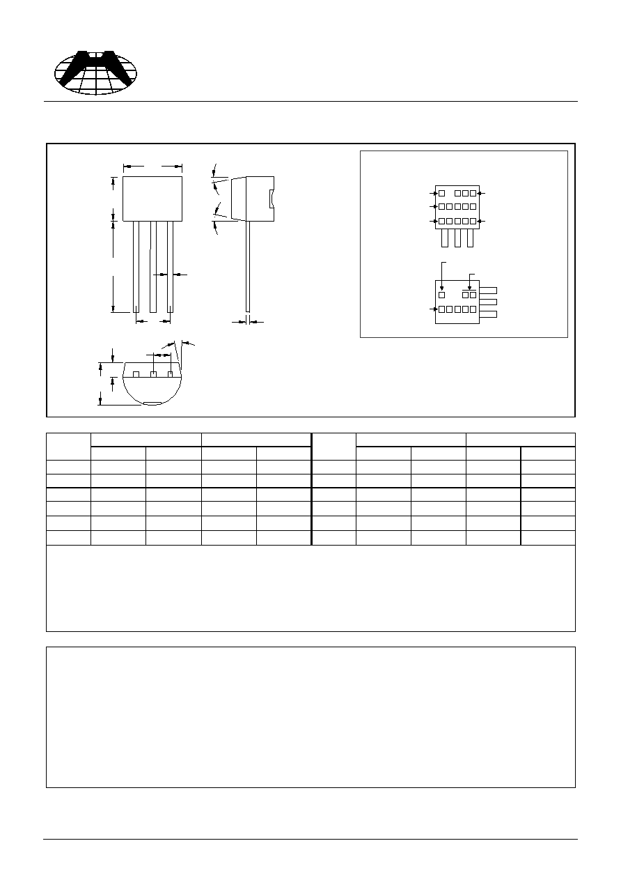
TO-92 Dimension
*:Typical
Inches
Millimeters
Inches
Millimeters
DIM
Min.
Max.
Min.
Max.
DIM
Min.
Max.
Min.
Max.
A
0.1704
0.1902
4.33
4.83
G
0.0142
0.0220
0.36
0.56
B
0.1704
0.1902
4.33
4.83
H
-
*0.1000
-
*2.54
C
0.5000
-
12.70
-
I
-
*0.0500
-
*1.27
D
0.0142
0.0220
0.36
0.56
1
-
*5
∞
-
*5
∞
E
-
*0.0500
-
*1.27
2
-
*2
∞
-
*2
∞
F
0.1323
0.1480
3.36
3.76
3
-
*2
∞
-
*2
∞
Notes :
1.Dimension and tolerance based on our Spec. dated Apr. 25,1996.
2.Controlling dimension : millimeters.
3.Maximum lead thickness includes lead finish thickness, and minimum lead thickness is the minimum thickness of base material.
4.If there is any question with packing specification or packing method, please contact your local HSMC sales office.
Material :
∑
Lead : 42 Alloy ; solder plating
∑
Mold Compound : Epoxy resin family, flammability solid burning class:UL94V-0
Important Notice:
∑
All rights are reserved. Reproduction in whole or in part is prohibited without the prior written approval of HSMC.
∑
HSMC reserves the right to make changes to its products without notice.
∑
HSMC semiconductor products are not warranted to be suitable for use in Life-Support Applications, or systems.
∑
HSMC assumes no liability for any consequence of customer product design, infringement of patents, or application assistance.
Head Office And Factory :
∑
Head Office (Hi-Sincerity Microelectronics Corp.) : 10F.,No. 61, Sec. 2, Chung-Shan N. Rd. Taipei Taiwan R.O.C.
Tel : 886-2-25212056 Fax : 886-2-25632712, 25368454
∑
Factory 1 : No. 38, Kuang Fu S. Rd., Fu-Kou Hsin-Chu Industrial Park Hsin-Chu Taiwan. R.O.C
Tel : 886-3-5983621~5 Fax : 886-3-5982931
∑
Factory 2 : No. 17-1, Ta-Tung Rd., Fu-Kou Hsin-Chu Industrial Park Hsin-Chu Taiwan. R.O.C
Tel : 886-3-5977061 Fax : 886-3-5979220
3
1
A
D
B
C
I
1
E
F
2
3
G
H
2
Style : Pin 1.Emitter 2.Base 3.Collector
3-Lead TO-92 Plastic Package
HSMC Package Code : A
Marking :
HSMC Logo
Part Number
Date Code
Product Series
Rank
Laser Mark
HSMC Logo
Part Number
Product Series
Ink Mark