 | –≠–ª–µ–∫—Ç—Ä–æ–Ω–Ω—ã–π –∫–æ–º–ø–æ–Ω–µ–Ω—Ç: H3842 | –°–∫–∞—á–∞—Ç—å:  PDF PDF  ZIP ZIP |

HI-SINCERITY
MICROELECTRONICS CORP.
Spec. No. : HP200202
Issued Date : 1998.08.01
Revised Date : 2002.12.03
Page No. : 1/10
H3842P
HSMC Product Specification
H3842P / HSMC3842
HIGH PERFORMANCE CURRENT MODE CONTROLERS
Description
The H3842P/HSMC3842 are high performance fixed frequency current mode
controllers. They are specifically designed for Off-Line and DC To DC converter
applications offering the designer a cost-effective solution with minimal external
components. These integrated circuits feature a trimmed oscillator for precise duty
cycle control. A temperature compensa-ted reference, high gain error amplifier,
current sensing comparator, and a high current totem pole output ideally suited for
driving a power MOSFET. Also included are protective features consisting of input and reference undervoltage
lockouts each with hysteresis, cycle-by-cycle current limiting, programmable output deadtime, and a latch for single
pulse metering.
Features
∑
Trimmed Oscillator for Precise Frequency Control
∑
Oscillator Frequency Guaranteed at 250 kHz
∑
Current Mode Operation to 500 kHz
∑
Automatic Feed Forward Compensation
∑
Latching PWM for Cycle-By-Cycle Current Limiting
∑
Internally Trimmed Reference with Undervoltage Lockout
∑
High Current Totem Pole Output
∑
Undervoltage Lockout with Hysteresis
∑
Low Startup and Operating Current
Absolute Maximum Ratings
Symbol
Parameter
Value
Unit
Vi
Supply Voltage (low impedance source)
30
V
Vi
Supply Voltage (Ii<30mA)
Self Limiting
Io
Output Current
±
1
A
Eo
Output Energy (capacitive load)
5
uJ
Analog Inputs (pin 2, 3)
-0.3 to 5.5
V
Error Amplifier Output Sink Current
10
mA
Ptot
Power Dissipation at Tamb
25
o
C
1.25
W
Tstg
Storage Temperature Range
-65 to 150
o
C
TJ
Junction Operating Temperature
-40 to 150
o
C
TL
Lead Temperature (soldering 10s)
300
o
C
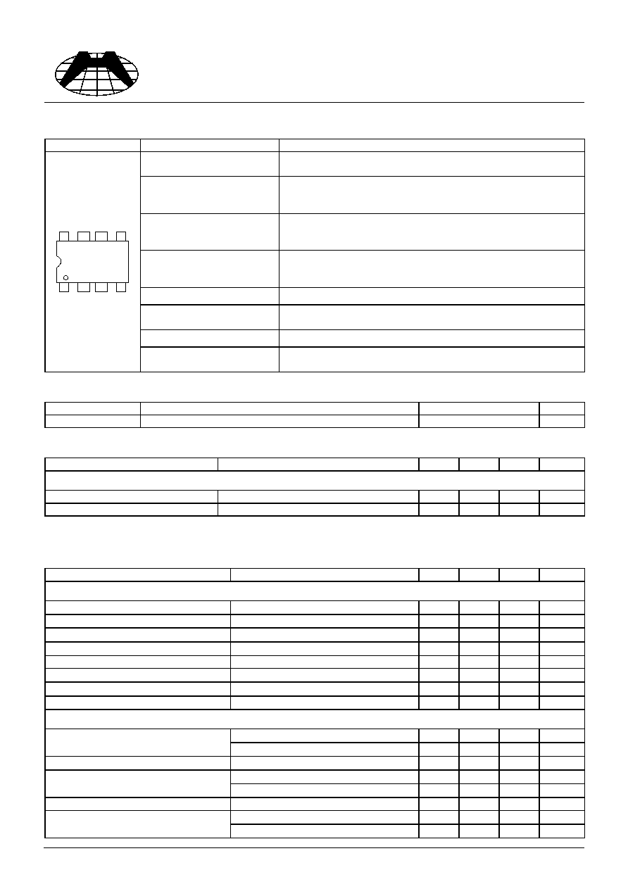
Block Diagram
DIP-8Pin
1V
34V
2R
R
1
2
3
4
5
6
7
8
Vcc
Ground
VFB
COMP
Current
Sense
+
-
Error AMP.
VREF Good
Logic
2.50V
Current
Sense
Comparator
T
UVLO
5V
REF
Internal
Bias
PWM Latch
Output
VREF
5V 50mA
S/R
RT/CT
S
R
OSC
HI-SINCERITY
MICROELECTRONICS CORP.
Spec. No. : HP200202
Issued Date : 1998.08.01
Revised Date : 2002.12.03
Page No. : 2/10
H3842P
HSMC Product Specification
Pin Connection
(Top View)
DIP-8P
Function
Description
Pin1: Compensation
This pin is the Error Amplifier output and is made available for
loop compensation.
Pin2: Voltage Feedback
This is the inverting input of the Error Amplifier. It's normally
connected to the switching power supply output through a
resistor divider.
Pin3: Current Sense
A voltage proportional to inductor current is connected to this
input. The PWM uses this information to terminate the output
switch conduction.
Pin4: RT/CT
The oscillator frequency and maximum output duty cycle are
programmed by connecting resistor RT to Vref and cpacitor CT
to ground. Operation to 500kHz is possible.
Pin5: Ground
This pin is the combined control circuitry and power ground.
Pin6: Output
This output directly drives the gate of a power MOSFET. Peak
currents up to 1A are sourced and sunk by this pin.
Pin7: Vcc
This pin is the positive supply of the control IC.
1
2
3
4
5
6
7
8
Pin8: Vref
This is the reference output. It provides charging current for
capacitor CT through resistor RT.
Thermal Data
Symbol
Description
Max.
Units
Rth j-amb
Thermal Resistance Junction-ambient
100
o
C/W
Electrical Specifications
Parameter
Test Conditions
Min.
Typ.
Max.
Units
Under-Voltage Lockout Section
Start Threshold
14.5
16
17.5
V
Min. Operating Voltage
After Turn On
8.5
10
11.5
V
Electrical Characteristics
Unless otherwise stated, specifications apply for 0
Ta
70
∞
C Vcc =15V
(Note 1)
; RT=680
, CT=0.022uF for
triangular mode, RT=10k, CT=3.3nf for sawtooth mode
Parameter
Test Conditions
Min.
Typ.
Max.
Units
Reference Section
Reference Output Voltage
Tj=25
∞
C,Io=1mA
4.90
5
5.1
V
Line Regulation
12V
Vin
25V
-
2.0
20
mV
Load Regulation
1mA
Io
20mA
-
3.0
25
mV
Temperature. Stability
(Note 2)
-
0.2
-
mV/
∞
C
Total Output Variation
Line , Load , Temp
(Note 2)
4.82
-
5.18
V
Output Noise Voltage
10Hz
f
10kHz,Tj=25
∞
C
(Note 2)
-
50
-
uV
Long Term Stability
Ta=125
∞
C,1000Hrs
(Note 2)
-
5
-
mV
Output Short current
Ta=25
∞
C
-30
-100
-180
mA
Oscillator Section
Tj=25
∞
C
47
52
57
KHz
Frequency
Tlow
Ta
Thigh
46
52
60
KHz
Frequency Chnge with Temperature
12V
Vcc
25V
-
0.2
1
%
Tlow
Ta
Thigh
(Note 2)
-
5
-
%
Frequency Change with Temperature
Tj=25
∞
C
-
0.5
-
%
Oscillator Voltage Swing
Peak to Peak
-
1.7
-
V
Tj=25
∞
C
7.8
8.3
9.3
mA
Discharge Current
Tlow
Ta
Thigh
7.2
-
9.5
mA

HI-SINCERITY
MICROELECTRONICS CORP.
Spec. No. : HP200202
Issued Date : 1998.08.01
Revised Date : 2002.12.03
Page No. : 3/10
H3842P
HSMC Product Specification
Parameter
Test Conditions
Min.
Typ.
Max.
Units
Error Amplifier Section
Voltage Feedback Input
Vo=2.5V
2.42
2.50
2.58
V
Input Bias Current
VFB=5.0V
-
-0.1
-2.0
uA
Open Loop Voltage Gain
2
Vo
4 V
65
90
-
dB
Unity Gain Bandwidth
Tj=25
∞
C
(Note 2)
0.7
1.0
-
MHz
Power Supply Rejection Ratio
12V
Vcc
25V
60
70
-
dB
Sink (Vo=1.1V, VFB=2.7V)
2.0
12
-
mA
Output Current
Source (Vo=5.0V, VFB=2.3V)
-0.5
-1.0
-
mA
Output Voltage Swing
High State
VFB=2.3V, RL=15K to ground
5
6
-
V
Low State
VFB=2.7V, RL=15K to Vref
-
0.7
1.1
V
Current Sense Section
Current Sense Input Voltage Gain
(Notes 3 & 4)
2.85
3.0
3.15
V/V
Maximum Current Sense Input
Thresold
(Note 3)
0.9
1.0
1.1
V
Ppwer Supply Rejection Ratio
12V
Vcc
25V
(Note 3)
-
70
-
dB
Input Bias Current
-
-2.0
-10
uA
Propagation Delay
Tj=25
∞
C
(Note 2)
-
150
300
nS
Output Section
Low State (Isink=20mA)
-
0.1
0.4
V
Low State (Isink=200mA)
-
1.5
2.2
V
High State (Isource=20mA)
13
13.5
-
V
Output Voltage
High State (Isource=200mA)
12
13.4
-
V
Output Voltage Rise Time
Tj=25
∞
C, CL=1.0nF
(Note 2)
-
50
150
nS
Output Voltage Fall Time
Tj=25
∞
C, CL=1.0nF
(Note 2)
-
50
150
nS
Output Voltage with UVLO Activated
Vcc=6V , Isink=1.0mA
-
-0.1
-1.1
V
Total Device
Start-Up Current
-
0.1
0.5
mA
Operating Supply Current
Vpin2=Vpin3=0, RT=10K, CT=3.3nF
-
11
17
mA
Vcc Zener Voltage
Icc=25 mA
-
34
-
V
Note 1: Adjust Vcc above the start threshold before setting at 15V.
Note 2: These parameters, although guaranteed are not 100% tested in production.
Note 3: Parameter measured at trip point of latch with Vpin2=0.
Note 4: Gain defined as: A=Vpin1/Vpin3, 0
Vpin3
0.8V
HI-SINCERITY
MICROELECTRONICS CORP.
Spec. No. : HP200202
Issued Date : 1998.08.01
Revised Date : 2002.12.03
Page No. : 4/10
H3842P
HSMC Product Specification
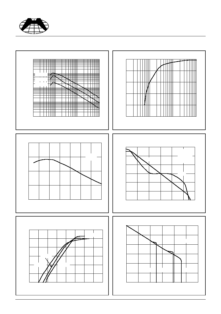
Characteristics Curve
Oscillator Frequency & Timing Resistance
1K
10K
100K
1000K
10000K
100
1000
10000
100000
RT()
fo
(
H
z
)
CT=1.0nF
CT=2.2nF
CT=4.7nF
Maximum Duty Cycle & Timing Resistance
0
20
40
60
80
100
100
1000
10000
100000
RT()
fo
(
H
z
)
Current Sense Input Threshold & Error Amp
Output Voltage
0
0.2
0.4
0.6
0.8
1
1.2
0
2
4
6
8
Vo (V)
Vt
h
(
V
)
Ta=125
o
C
Ta=-40
o
C
Ta=25
o
C
Vcc=15V
Reference Voltage Change & Source Current
0
10
20
30
40
50
60
0
20
40
60
80
100
120
Iref (mA)
Ta=125
o
C
Ta=25
o
C
Ta=-40
o
C
Vcc=15V
Oscillator Discharge Current & Temperate
7
7.5
8
8.5
9
-50
-25
0
25
50
75
100
125
TA (
o
C)
I
d
i
sch
g
(
m
A
)
Vi=15V
Vosc=2V
Error Amp Open-Loop Gain and Phase &
Frequency
-20
0
20
40
60
80
100
10
100
1000
10000
100000 1000000 10000000
f (Hz)
(d
B
)
Gain
Phase
Vcc=15V
Vo=2V to 4V
R
L
=100K
Ta=25
o
C
30
60
90
120
150
180

HI-SINCERITY
MICROELECTRONICS CORP.
Spec. No. : HP200202
Issued Date : 1998.08.01
Revised Date : 2002.12.03
Page No. : 5/10
H3842P
HSMC Product Specification
Reference Short Circuit Current &Temperature
50
60
70
80
90
100
110
-50
-25
0
25
50
75
100
125
TA (
o
C)
I
sc (
m
A
)
Vcc=15V
RL0.1
Supply Current & Supply Voltage
0
5
10
15
20
25
0
10
20
30
40
Vi (V)
Ii
(
m
A
)
R
T
=10K
C
T
=3.3nF
Output Saturation Voltage & Load Current
0
1
2
3
4
0
200
400
600
800
Io (mA)
Vs
a
t
(
V
)
Sink Saturation
(Load to Vcc)
Ta=-40
o
C
Ta=25
o
C
Vcc=15V
80us Pulsed Load
120Hz Rate
Output Saturation Voltage & Load Current
-4
-3
-2
-1
0
0
200
400
600
800
Io (mA)
Vs
a
t
(
V
)
Source Saturation
(Load to Ground)
Ta=25
o
C
Ta=-40
o
C
Vcc=15V
80us Pulsed Load
120Hz Rate