 | –≠–ª–µ–∫—Ç—Ä–æ–Ω–Ω—ã–π –∫–æ–º–ø–æ–Ω–µ–Ω—Ç: H431 | –°–∫–∞—á–∞—Ç—å:  PDF PDF  ZIP ZIP |
HI-SINCERITY
MICROELECTRONICS CORP.
Spec. No. : HA200216
Issued Date : 1998.04.08
Revised Date : 2002.08.27
Page No. : 1/4
H431AA, H431BA, H431CA
HSMC Product Specification
H431AA/BA/CA
AJDUSTABLE SHUNT REGULATOR
Description
The H431 series are three-terminal adjustable regulators with guara-
nteed thermal stability over applicable temperature ranges. The out-
put voltage may be set to any value between V
REF
(approximately
2.495 volts) and 36 volts with two external resistors. These devices
have a typical dynamic output impedance of 0.2
. Active output circ-
uitry provides a very sharp turn-on characteristic, making these devices excellent replacement for
zener diodes in many applications.
Features
∑
Programmable output voltage
∑
Temperature coefficient is 50ppm/
∞
C typical
∑
Temperature compensated for operation over
∑
full temperature range
∑
Low output noise voltage
∑
Fast turn on response
Classification
Rank
A
B
C
V
REF
2.495
±
2%
2.495
±
1%
2.495
±
0.5%
Absolute Maximum Ratings
(Operating temperature range applies unless otherwise specified)
Characteristics
Symbol
Value
Unit
Cathode Voltage
V
KA
37
V
Cathode Current Range (Continuous)
I
K
-100~+150
mA
Reference Input Current Range
I
REF
0.05~+10
mA
Power Dissipation
P
D
770
mW
Operating Temperature Range
T
opr
0~+70
∞
C
Storage Temperature Range
T
stg
-65~+150
∞
C
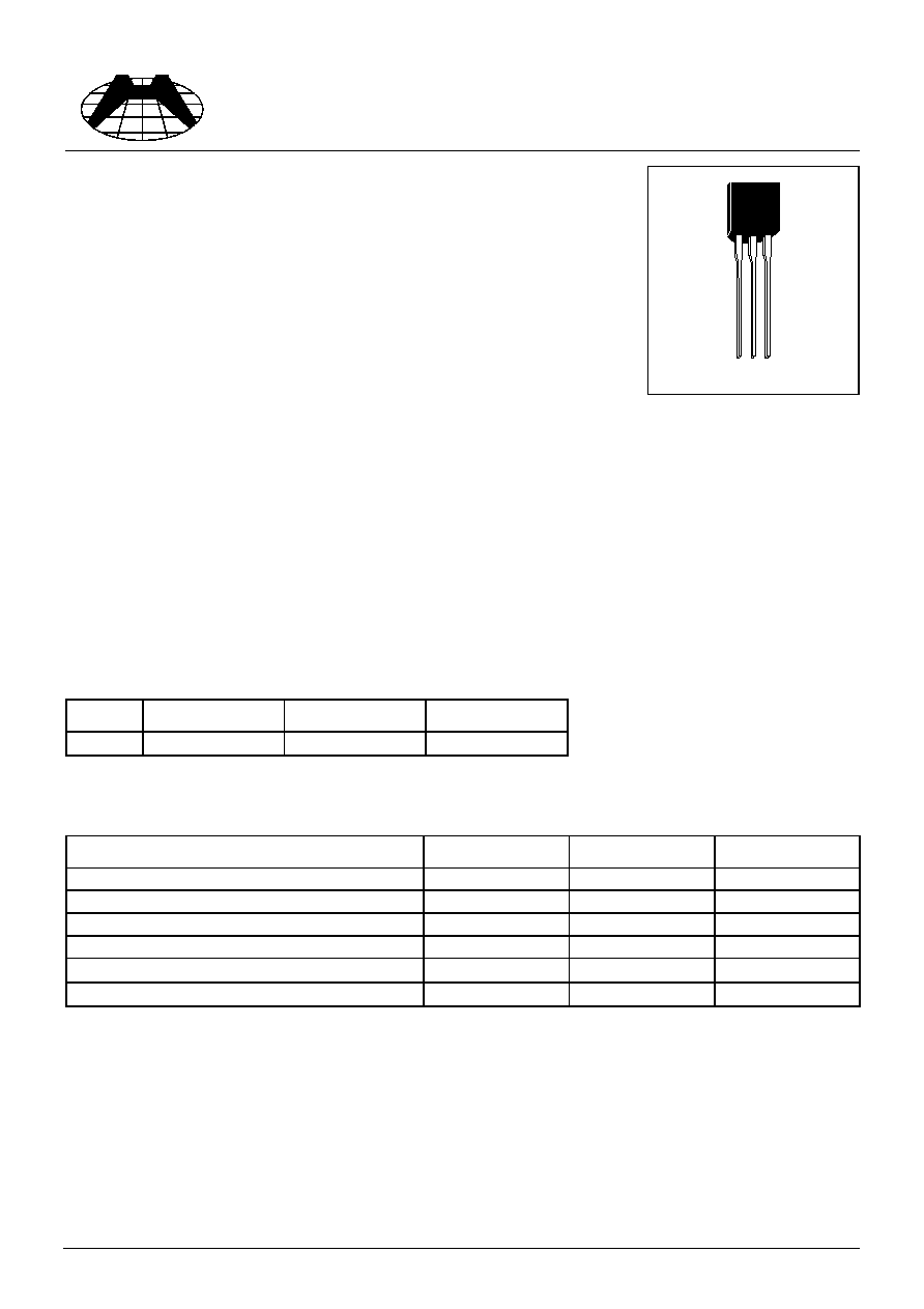
TO-92
HI-SINCERITY
MICROELECTRONICS CORP.
Spec. No. : HA200216
Issued Date : 1998.04.08
Revised Date : 2002.08.27
Page No. : 2/4
H431AA, H431BA, H431CA
HSMC Product Specification
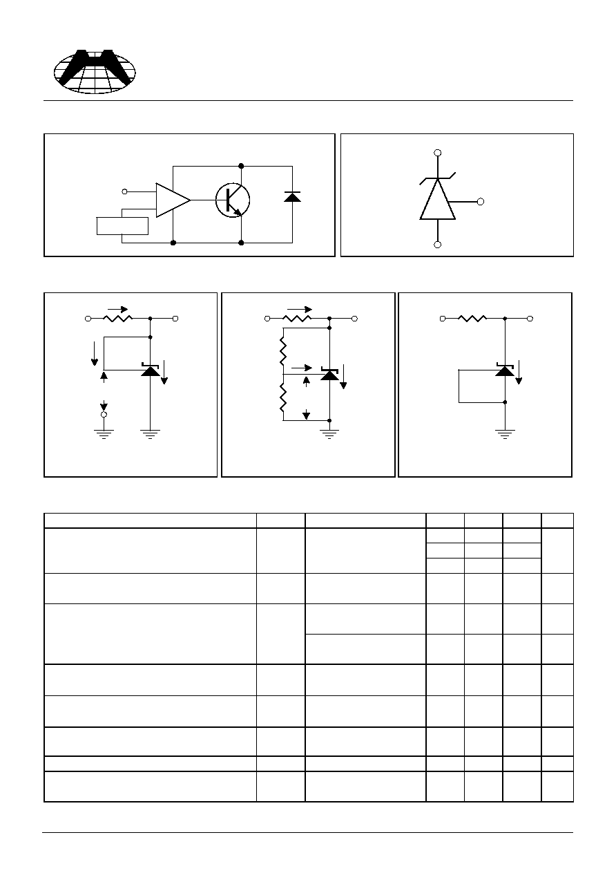
Functional Block Diagram & Symbol
Test Circuits
Electrical Characteristics
( Ta=25
∞
C unless otherwise specified )
Characteristics
Symbol
Test Conditions
Min
Typ
Max Unit
H431AA
2.445 2.495 2.545
H431BA
2.470 2.495 2.520
Reference Input Voltage
H431CA
V
REF
V
KA
=V
REF
, I
K
=10mA
2.480 2.495 2.510
V
Deviation of Reference Input Voltage
Over-Temperature
V
REF(dev)
V
KA
=V
REF
, I
K
=10mA
T
min
T
a
T
max
-
4
17
mV
I
K
=10mA,
V
KA
=10V-V
REF
-
-1.4
-2.7
mV
Ratio of Change in Reference Input
Voltage to the Change in Cathode
Voltage
V
REF
/
V
KA
I
K
=10mA,
K
KA
=36V-10V
-
-1.0
-2.0
V
Reference Input Current
I
REF
I
K
=10mA, R
1
=10k
,
R
2
=
-
2
4
uA
Deviation of Reference Input Current
Over Full Temperature Range
I
REF(dev)
I
K
=10mA, R
1
=10k
,
R
2
=
, T
a
=Full Range
-
0.4
1.2
uA
Minimum Cathode Current for
Regulation
I
K(min)
V
KA
=V
REF
-
0.4
1.0
mA
Off-State Cathode Current
I
K(off)
V
KA
=36V, V
REF
=0
-
0.1
1.0
uA
Dynamic impedance
Z
KA
V
KA
=V
REF
, f
1.0KHz
I
K
=1 to 100mA
-
0.2
0.5
Functional Block Diagram :
Symbol :
Cathode
Reference
Anode
Cathode
V
REF
+
-
Reference
Anode
IN
V
Z
I
I
I
REF
V
REF
I
Z
R1
Fig1. Test Circuit for V
Z
=V
REF
I
I
V
Z
IN
I
REF
I
Z
R2
V
REF
Fig 2. Test Circuit for V
Z
>V
REF
Note : V
Z
=V
REF
(1+R
1
/R
2
)+I
REF
xR
1
IN
V
Z
Fig3. Test Circuit for Off-State
Current
HI-SINCERITY
MICROELECTRONICS CORP.
Spec. No. : HA200216
Issued Date : 1998.04.08
Revised Date : 2002.08.27
Page No. : 3/4
H431AA, H431BA, H431CA
HSMC Product Specification
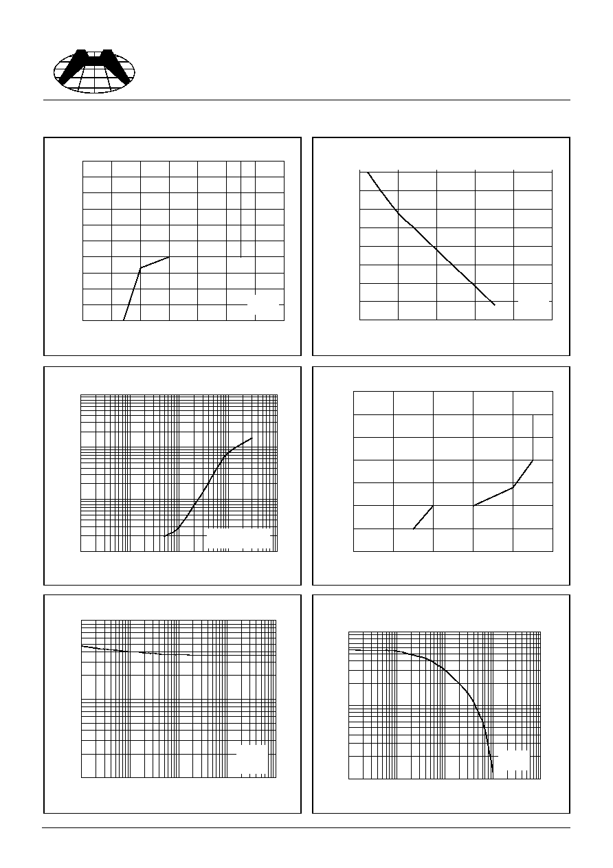
Characteristics Curve
Cathode Current & Cathode Voltage
-100
-75
-50
-25
0
25
50
75
100
125
150
-3
-2
-1
0
1
2
3
4
Cathode Voltage (V)
C
a
t
h
o
de C
u
r
r
en
t
(
m
A
)
V
KA
=V
ref
TA=25∫C
Change in Reference Input Voltage
& Cathode Voltage
-40
-35
-30
-25
-20
-15
-10
-5
0
0
10
20
30
40
50
Cathode Voltage (V)
C
h
an
g
e
i
n
R
e
f
e
r
e
n
c
e I
n
pu
t
V
o
l
t
ag
e
(m
V
)
I
K
=10m
TA=25∫C
Dynamic Impedance & Frequence
0.1
1
10
100
1
10
100
1000
10000
Frequency (Hz)
I
m
peda
n
c
e (
o
h
m
)
I
K
=10mA to 100mA
TA=25∫C
Cathode Current & Cathode Voltage
-400
-200
0
200
400
600
800
1000
-2
-1
0
1
2
3
Cathode Voltage (V)
C
a
t
h
ode C
u
r
r
en
t
(
u
A
)
V
KA
=V
ref
TA=25∫C
Noise Voltage & Frequency
1
10
100
10
100
1000
10000
100000
Frequency (Hz)
N
o
i
s
e V
o
l
t
age
(
n
V
/
H
z
1/
2
)
V
KA
=V
ref
I
K
=10mA
TA=25∫C
Small Signal Voltage Amplification
& Frequency
1
10
100
1000
10000
100000
1000000
10000000
Frequency (Hz)
V
o
l
t
ag
e A
m
pl
i
f
i
c
at
i
o
n
(
d
B
)
IK=10mA
TA=25∫C
HI-SINCERITY
MICROELECTRONICS CORP.
Spec. No. : HA200216
Issued Date : 1998.04.08
Revised Date : 2002.08.27
Page No. : 4/4
H431AA, H431BA, H431CA
HSMC Product Specification
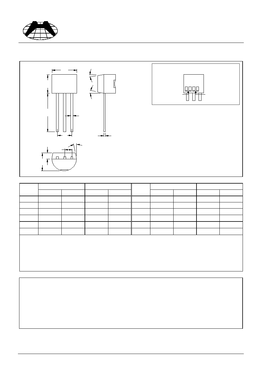
TO-92 Dimension
*: Typical
Inches
Millimeters
Inches
Millimeters
DIM
Min.
Max.
Min.
Max.
DIM
Min.
Max.
Min.
Max.
A
0.1704
0.1902
4.33
4.83
G
0.0142
0.0220
0.36
0.56
B
0.1704
0.1902
4.33
4.83
H
-
*
0.1000
-
*
2.54
C
0.5000
-
12.70
-
I
-
*
0.0500
-
*
1.27
D
0.0142
0.0220
0.36
0.56
1
-
*
5
∞
-
*
5
∞
E
-
*
0.0500
-
*
1.27
2
-
*
2
∞
-
*
2
∞
F
0.1323
0.1480
3.36
3.76
3
-
*
2
∞
-
*
2
∞
Notes:
1.Dimension and tolerance based on our Spec. dated Apr. 25,1996.
2.Controlling dimension: millimeters.
3.Maximum lead thickness includes lead finish thickness, and minimum lead thickness is the minimum thickness of base material.
4.If there is any question with packing specification or packing method, please contact your local HSMC sales office.
Material:
∑
Lead: 42 Alloy; solder plating
∑
Mold Compound: Epoxy resin family, flammability solid burning class: UL94V-0
Important Notice:
∑
All rights are reserved. Reproduction in whole or in part is prohibited without the prior written approval of HSMC.
∑
HSMC reserves the right to make changes to its products without notice.
∑
HSMC semiconductor products are not warranted to be suitable for use in Life-Support Applications, or systems.
∑
HSMC assumes no liability for any consequence of customer product design, infringement of patents, or application assistance.
Head Office And Factory:
∑
Head Office (Hi-Sincerity Microelectronics Corp.) : 10F.,No. 61, Sec. 2, Chung-Shan N. Rd. Taipei Taiwan R.O.C.
Tel: 886-2-25212056 Fax: 886-2-25632712, 25368454
∑
Factory 1: No. 38, Kuang Fu S. Rd., Fu-Kou Hsin-Chu Industrial Park Hsin-Chu Taiwan. R.O.C
Tel: 886-3-5983621~5 Fax: 886-3-5982931
3
1
A
D
B
C
I
1
E
F
2
3
G
H
2
Style: Pin 1.Reference 2.Anode 3.Cathode
3-Lead TO-92 Plastic Package
HSMC Package Code: A
Marking:
H
A
3
4
1
Date Code
Control Code