 | –≠–ª–µ–∫—Ç—Ä–æ–Ω–Ω—ã–π –∫–æ–º–ø–æ–Ω–µ–Ω—Ç: H603AL | –°–∫–∞—á–∞—Ç—å:  PDF PDF  ZIP ZIP |
HI-SINCERITY
MICROELECTRONICS CORP.
Spec. No. : Preliminary Data
Issued Date : 1998.07.01
Revised Date : 1999.08.01
Page No. : 1/5
HSMC Product Specification
H603AL
N-Channel Logic Level Enhancement Mode Field Effect Transistor
Description
This very high density process has been especially tailored to minimize on-
state resistance and provide superior switching performance. These
devices are particularly suited for low voltage applications such as DC/DC
converters and other battery powered circuits where fast switching, low in-
line power loss, and resistance to transients are needed.
Absolute Maximum Ratings
(Ta=25
∞
C)
∑
Maximum Temperatures
Operating and Storage Temperature ................................................................................ -65 ~ +175
∞
C
∑
Maximum Power Dissipation
Total Power Dissipation at Tc=25
∞
C ............................................................................................... 60 W
Derate Above 25
∞
C ................................................................................................................ 0.4 W /
∞
C
∑
Maximum Voltages and Currents
Drain-Source Voltage...................................................................................................................... 30 V
Gate-Source Voltage -Continuous................................................................................................
±
20 V
Drain Current -Continuous .............................................................................................................. 30 A
Drain Current -Pulsed ................................................................................................................... 100 A
Thermal Resistance, Junction-to-Case .................................................................................. 2.5
∞
C / W
Thermal Resistance, Junction-to-Ambient............................................................................ 62.5
∞
C / W
Electrical Characteristics
∑
Off Characteristics
Symbol
Parameter
Condition
Min
Typ
Max Unit
BV
DSS
Drain-Source Breakdown Voltage
V
GS
=0V, I
D
=250uA
30
-
-
V
I
DSS
Zero Gate Voltage Drain Current
V
DS
=30V, V
GS
=0V
-
-
10
uA
+I
GSS
Gate-Body Leakage, Forward
V
GS
=20V, V
DS
=0V
-
-
100
nA
-I
GSS
Gate-Body Leakage, Reverse
V
GS
=-20V, V
DS
=0V
-
-
-100
nA
∑
On Characteristics
V
DS
=V
GS
, I
D
=250uA
1.1
-
3
V
GS(TH)
Gate Threshold Voltage
V
DS
=V
GS
, I
D
=10mA
1.4
-
3
V
V
GS
=10V, I
D
=25A
-
0.018 0.022
R
DS
(on) Static Drain-Source On-Resistance
V
GS
=4.5V, I
D
=10A
-
0.029 0.040
V
GS
=10V, V
DS
=10V
60
-
-
I
DS
(on)
On-State Drain Current
V
GS
=4.5V, V
DS
=10V
15
-
-
A
g
FS
Forward Transconductance
V
DS
=10V, I
D
=25A
-
26
-
S
∑
Dynamic Characteristic
C
iss
Input Capacitance
-
1100
-
pF
C
oss
Output Capacitance
-
600
-
pF
C
rss
Reverse Transfer Capacitance
V
DS
=15V, V
GS
=0V
f=1.0Mhz
-
180
-
pF
HI-SINCERITY
MICROELECTRONICS CORP.
Spec. No. : Preliminary Data
Issued Date : 1998.07.01
Revised Date : 1999.08.01
Page No. : 2/5
HSMC Product Specification
∑
Switching Characteristics
Symbol
Parameter
Condition
Min
Typ
Max Unit
Turn-On Delay Time
-
-
30
ns
T(on)
Turn-On Rise Time
-
-
110
ns
Turn-Off Delay Time
-
-
150
ns
T(off)
Turn-Off Fall Time
V
DS
=15V, I
D
=25A
V
GS
=10V, R
GEN
=24
-
-
130
ns
Q
g
Total Gate Charge
-
-
45
nC
Q
gs
Gate-Source Charge
-
-
10
nC
Q
gd
Gate-Drain Charge
V
DS
=10V, I
D
=25A,
V
GS
=10V
-
-
10
nC
∑
Drain-Source Diode Characteristics And Maximum Ratings
Maximum Continuous Drain-Source Diode Forward Current
-
-
25
A
V
SD
Drain-Source Diode Forward Voltage
V
GS
=0V, I
S
=25A
-
-
1.3
V
Characteristics Curve
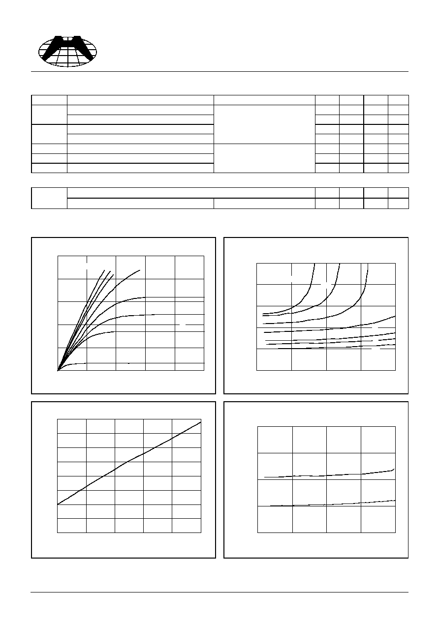
On-Region Characteristic
0
20
40
60
80
100
0
1
2
3
4
5
Drain-Source Voltage (V)
D
r
a
i
n-
S
o
ur
c
e
C
u
r
r
e
n
t
(
A
)
VGS=10V 8V
5V
6V
7V
3V
4.5V
4V
On-Resistance Variation With Gate Voltage &
Drain Current
0.5
1.0
1.5
2.0
2.5
3.0
0
20
40
60
80
Drain Current (A)
N
o
r
m
a
l
iz
e
d
Dr
a
i
n
-
S
o
u
r
c
e
O
n
-
R
e
si
st
a
n
ce
8V
7V
6V
5 V
4.5V
VGS= 4V
10V
On Resistance Variation & Temperature
0.8
0.9
1.0
1.1
1.2
1.3
1.4
1.5
1.6
25
50
75
100
125
150
Junction Temperature (∞C)
N
o
r
m
al
i
z
e
d
D
r
ai
n
-
S
o
u
r
c
e
O
n
-
R
es
i
s
t
a
n
c
e
ID=25A
VGS=10V
On-Resistance Variation & Drain Current &
Temperature
0.5
1
1.5
2
2.5
0
20
40
60
80
Drain Current (A)
N
o
r
m
a
l
iz
e
d
Dr
a
i
n
-
S
o
u
r
c
e
O
n
-
R
e
si
st
a
n
ce
VGS=10V
TJ=125∞C
TJ=25∞C
HI-SINCERITY
MICROELECTRONICS CORP.
Spec. No. : Preliminary Data
Issued Date : 1998.07.01
Revised Date : 1999.08.01
Page No. : 3/5
HSMC Product Specification
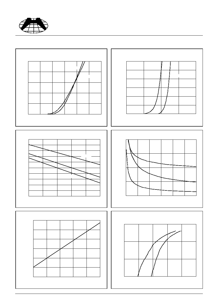
Drain Current Variation & Gate Voltage &
Temperature
0
10
20
30
40
50
0
1
2
3
4
5
6
Gate-Source Voltage (V)
Dr
a
i
n
Cu
r
r
e
n
t
(
A
)
TJ=125∞C
TJ= 25∞C
Sub-Threshold Drain Current Variation & Gate
Voltage & Temperature
0
0.01
0.02
0.03
0.04
0.05
0.06
0.5
1.0
1.5
2.0
2.5
Gate-Source Voltage (V)
Dr
a
i
n
Cu
r
r
e
n
t
(
A
)
TJ=125∞C
TJ=25∞C
Gate Threshold Variation & Temperature
0.8
0.9
1
1.1
1.2
1.3
1.4
1.5
1.6
1.7
1.8
25
50
75
100
125
150
Junction Temperature (∞C)
G
a
t
e
-
S
ou
r
c
e T
h
r
e
s
h
ol
d V
o
l
t
ag
e (
V
)
ID=10mA
ID= 250uA
ID=1mA
Capacitance Characteristics
0
500
1000
1500
2000
0
5
10
15
20
25
30
Drain-Source Voltage (V)
Ca
p
a
c
i
t
a
n
c
e
(
p
F
)
Ciss
Crss
Coss
Breakdown Voltage Variation & Temperature
0.98
1
1.02
1.04
1.06
1.08
1.1
25
50
75
100
125
150
Junction Temperature (∞C)
N
o
r
m
al
i
z
e
d
D
r
ai
n
-
S
o
u
r
c
e
B
r
ea
k
dow
n
V
o
l
t
age
Body Diode Forward Voltage Variation &
Current & Temperature
0.1
1
10
100
0.2
0.4
0.6
0.8
1
1.2
Body Diode Forward Voltage (V)
R
e
v
e
rs
e
D
r
a
i
n
C
u
rr
e
n
t
(A
)
TJ=125∞C
TJ= 25∞C
HI-SINCERITY
MICROELECTRONICS CORP.
Spec. No. : Preliminary Data
Issued Date : 1998.07.01
Revised Date : 1999.08.01
Page No. : 4/5
HSMC Product Specification
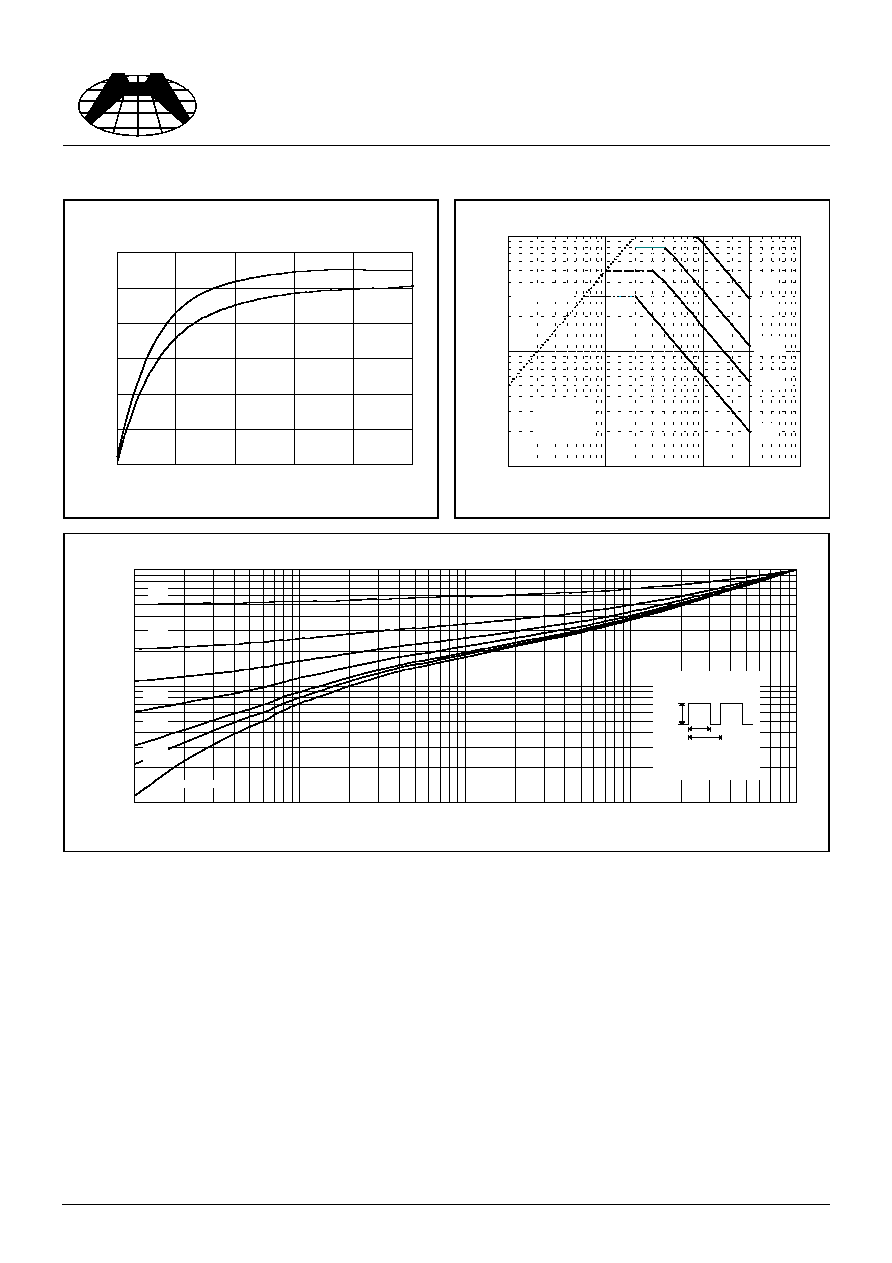
Trancient Thermal Response Curve
0.01
0.1
1
0.1
1
10
100
1000
Time (ms)
N
o
r
m
al
i
z
e
d
E
f
f
e
c
t
i
v
e T
r
an
s
i
en
t
T
h
e
r
m
a
l
R
e
si
st
a
n
ce
0.01
0.1
0.05
0.02
0.2
0.5
Single Pulse
R
JC(t) = r(t) * R
JC(t)
R
JC =2.5
∞
C / W
t2
P(pk)
t1
TJ-TC=P* R
JC(t)
Duty Cycle,D=t1/t2
Transductance Variation & Drain Current &
Temperature
0
5
10
15
20
25
30
0
10
20
30
40
50
Drain Current (A)
T
r
a
n
s
c
o
nd
uc
t
a
nc
e
(
S
)
TJ=25∞C
TJ=125∞C
Maximum Safe Operating Area
1
10
100
0.1
1
10
100
Drain-Source Voltage (V)
D
r
a
i
n-
S
o
ur
c
e
C
u
r
r
e
n
t
(
A
)
VGS=20V
Single Pulse
TC=25∞C
Rds(on) Line
Dc
100ms
10ms
1ms
1us
HI-SINCERITY
MICROELECTRONICS CORP.
Spec. No. : Preliminary Data
Issued Date : 1998.07.01
Revised Date : 1999.08.01
Page No. : 5/5
HSMC Product Specification
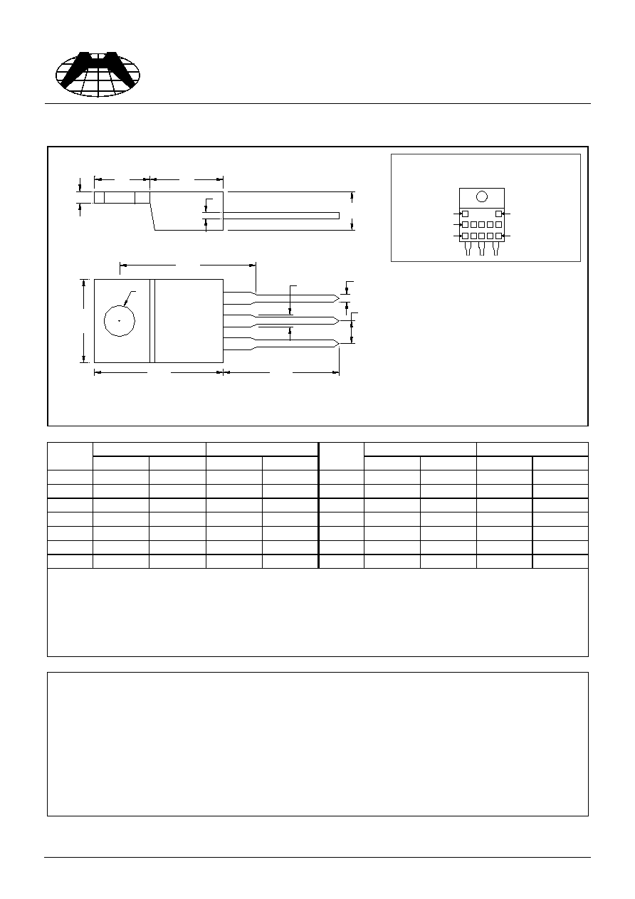
TO-220AB Dimension
*:Typical
Inches
Millimeters
Inches
Millimeters
DIM
Min.
Max.
Min.
Max.
DIM
Min.
Max.
Min.
Max.
A
0.2197
0.2949
5.58
7.49
I
-
*0.1508
-
*3.83
B
0.3299
0.3504
8.38
8.90
K
0.0295
0.0374
0.75
0.95
C
0.1732
0.185
4.40
4.70
M
0.0449
0.0551
1.14
1.40
D
0.0453
0.0547
1.15
1.39
N
-
*0.1000
-
*2.54
E
0.0138
0.0236
0.35
0.60
O
0.5000
0.5618
12.70
14.27
G
0.3803
0.4047
9.66
10.28
P
0.5701
0.6248
14.48
15.87
H
-
*0.6398
-
*16.25
Notes :
1.Dimension and tolerance based on our Spec. dated Sep. 07,1997.
2.Controlling dimension : millimeters.
3.Maximum lead thickness includes lead finish thickness, and minimum lead thickness is the minimum thickness of base material.
4.If there is any question with packing specification or packing method, please contact your local HSMC sales office.
Material :
∑
Lead : 42 Alloy ; solder plating
∑
Mold Compound : Epoxy resin family, flammability solid burning class:UL94V-0
Important Notice:
∑
All rights are reserved. Reproduction in whole or in part is prohibited without the prior written approval of HSMC.
∑
HSMC reserves the right to make changes to its products without notice.
∑
HSMC semiconductor products are not warranted to be suitable for use in Life-Support Applications, or systems.
∑
HSMC assumes no liability for any consequence of customer product design, infringement of patents, or application assistance.
Head Office And Factory :
∑
Head Office (Hi-Sincerity Microelectronics Corp.) : 10F.,No. 61, Sec. 2, Chung-Shan N. Rd. Taipei Taiwan R.O.C.
Tel : 886-2-25212056 Fax : 886-2-25632712, 25368454
∑
Factory 1 : No. 38, Kuang Fu S. Rd., Fu-Kou Hsin-Chu Industrial Park Hsin-Chu Taiwan. R.O.C
Tel : 886-3-5983621~5 Fax : 886-3-5982931
∑
Factory 2 : No. 17-1, Ta-Tung Rd., Fu-Kou Hsin-Chu Industrial Park Hsin-Chu Taiwan. R.O.C
Tel : 886-3-5977061 Fax : 886-3-5979220
A
B
E
G
I
K
M
O
P
3
2
1
C
N
H
D
4
Style : Pin 1.Gate 2.Drain 3.Source
3-Lead TO-220AB Plastic Package
HSMC Package Code : E
Marking :
HSMC Logo
Part Number
Date Code
Product Series
Rank