HI-SINCERITY
MICROELECTRONICS CORP.
Spec. No. : Preliminary Data
Issued Date : 1998.08.01
Revised Date : 2001.07.20
Page No. : 1/3
H7809AI, H7809BI
HSMC Product Specification
H7809AI
H7809BI
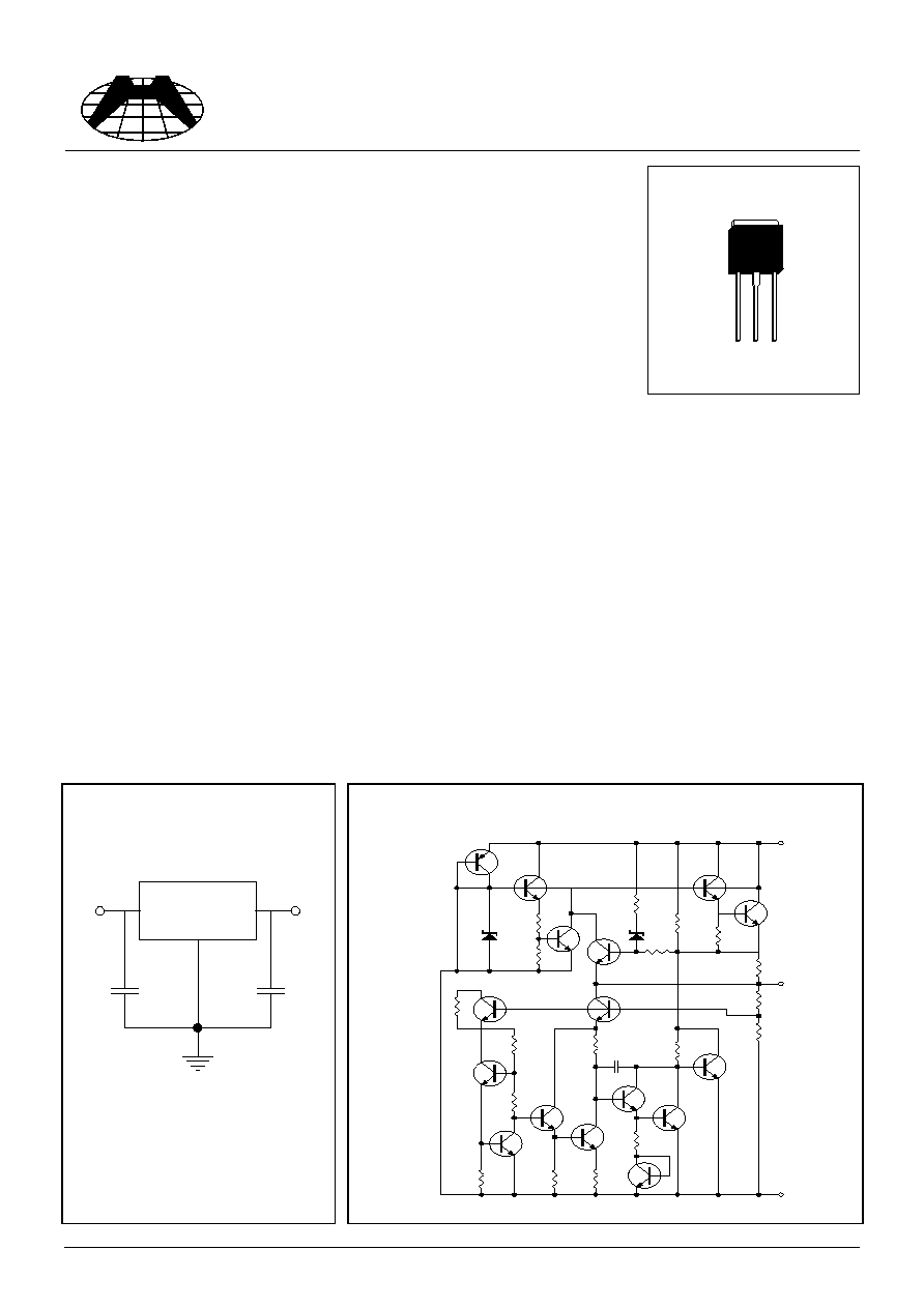
3-TERMINAL POSITIVE VOLTAGE REGULATOR
Description
The H7809_I series of three-terminal positive regulators are available
in the TO-251 package and with several fixed output voltages, making
it useful in a wide range of applications. These regulators can provide local on-card regulation,
eliminating the distribution problems associated with single point regulation. Each type employs
internal current limiting, thermal shut-down and safe operating area protection, making it essent-
ially indestructible. If adequate heat sinking is provided, they can deliver over 1A output current.
Although designed primarily as fixed voltage regulators, these devices can be used with external
components to obtain adjustable voltages and currents.
H7809_I is characterized for operation from 0
∞
C to +125
∞
C, and if operating temperature will al-
ways hi, please refer the power dissipation curve.
Absolute Maximum Ratings
(Ta=25
∞
C)
∑
Input Voltage.......................................................................... 35 V (5V Through 9V), 40 V (24V)
∑
Total Power Dissipation ............................................................................................Internal limit
∑
Operating Temperature Range ...............................................................................0
∞
C to +70
∞
C
∑
Maximum Junction Temperature........................................................................................125
∞
C
∑
Storage Temperature Range .............................................................................-55
∞
C to +150
∞
C
∑
Lead Temperature (Soldering 10S)....................................................................................230
∞
C
Typical Application
Schematic Diagram
H7809_I
Vout
Vin
3
1
2
C1
C2
Note :
C1 and C2 are required if regulator is
located far from power supply filter
and load, or oscillation may induced
on the loop.
6.3V
3.4K
200
10K
200
1K
2K
0.3
26
4K
20pF
4K
1K
12.1K
1.2
26
1.9K
30K
VREF
Input
Output
GND
HI-SINCERITY
MICROELECTRONICS CORP.
Spec. No. : Preliminary Data
Issued Date : 1998.08.01
Revised Date : 2001.07.20
Page No. : 2/3
H7809AI, H7809BI
HSMC Product Specification
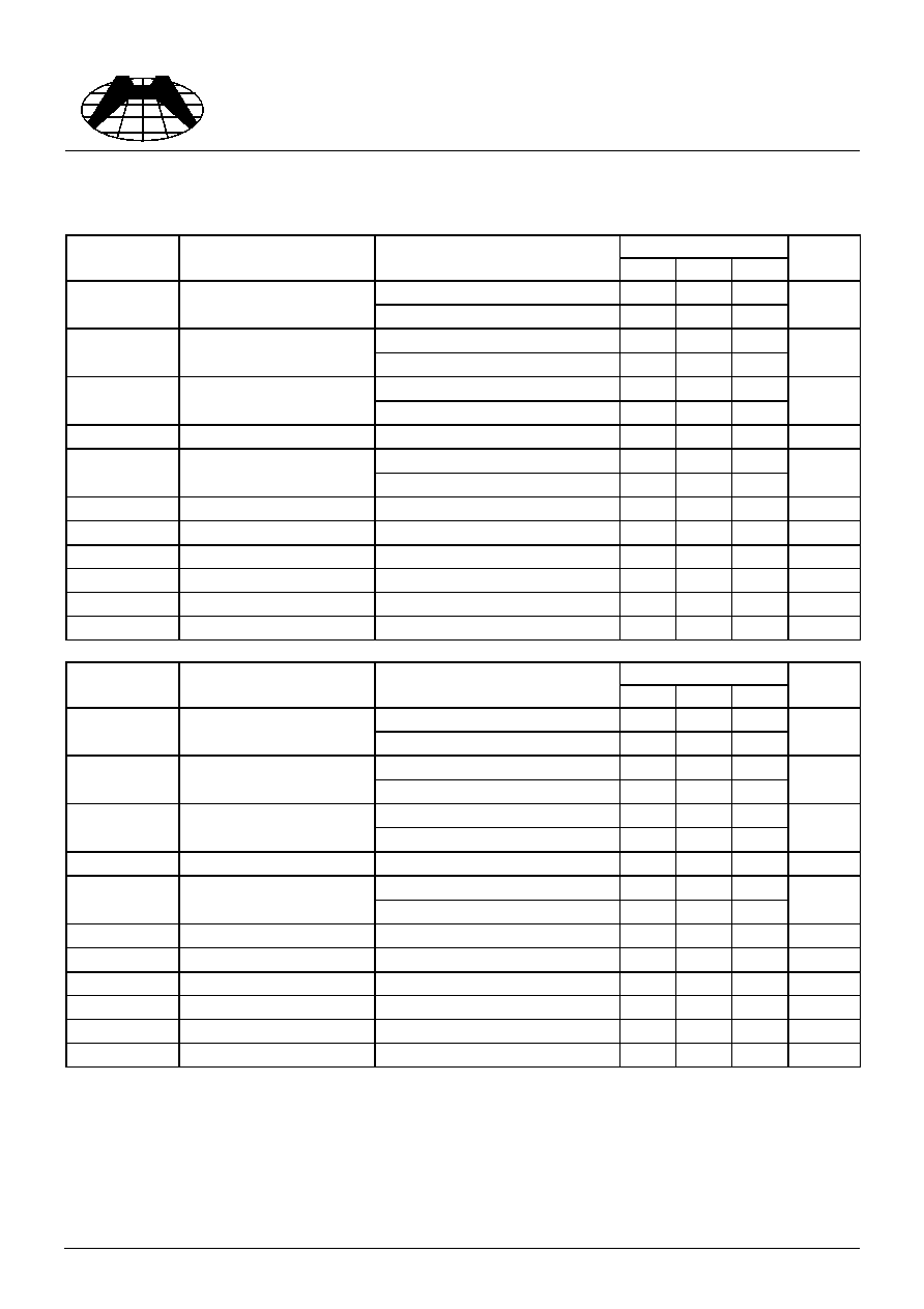
Electrical Characteristics
Vin=15V, Io=500mA, 0
∞
C
Tj
125
∞
C (unless otherwise noted)
H7809AI
Symbol
Parameter
Conditions
Min
Typ
Max
Units
Tj=25
∞
C
8.73
9
9.27
Vo
Output Voltage
PD
15W, 5mA
Io
1A
8.73
9
9.27
V
Tj=25
∞
C, 11.5V
Vin
25V
-
6
90
Vo
Line Regulation
Tj=25
∞
C, 12V
Vin
25V
-
2
45
mV
5mA
Io
1A
-
-
100
Vo
Load Regulation
250mA
Io
750mA
-
-
50
mV
IQ
Quiescent Current
Io
1A, Tj=25
∞
C
-
5.5
8
mA
5mA
Io
1A
-
-
0.5
IQ
Quiescent Current
Change
11.5V
Vin
26V
-
-
1.3
mA
Vn
Output Noise Voltage Ta=25
∞
C, 10Hz
f
100KHz
-
-
200
uV
RR
Ripple Rejection
13V
Vin
23V, f=120Hz
-
68
-
dB
VD
Dropout Voltage
Tj=25
∞
C, Io=1A
-
2
-
V
Isc
Short Circuit Current
Tj=25
∞
C
-
1.5
-
A
Ipk
Peak Output Current
Tj=25
∞
C
1.7
-
-
A
Vo /
T
Average Tc of Vout
0
∞
C
Tj
+125
∞
C, Io=5mA
-
-0.8
-
mV/
∞
C
H7809BI
Symbol
Parameter
Conditions
Min
Typ
Max
Units
Tj=25
∞
C
8.64
9
9.36
Vo
Output Voltage
PD
15W, 5mA
Io
1A
8.55
9
9.45
V
Tj=25
∞
C, 11.5V
Vin
25V
-
4
100
Vo
Line Regulation
Tj=25
∞
C, 12V
Vin
25V
-
2
50
mV
5mA
Io
1A
-
-
180
Vo
Load Regulation
250mA
Io
750mA
-
-
90
mV
IQ
Quiescent Current
Io
1A, Tj=25
∞
C
-
5.5
8
mA
5mA
Io
1A
-
-
0.5
IQ
Quiescent Current
Change
11.5V
Vin
26V
-
-
1.3
mA
Vn
Output Noise Voltage Ta=25
∞
C, 10Hz
f
100KHz
-
-
300
uV
RR
Ripple Rejection
13V
Vin
23V, f=120Hz
62
73
-
dB
VD
Dropout Voltage
Tj=25
∞
C, Io=1A
-
2.5
-
V
Isc
Short Circuit Current
Tj=25
∞
C
-
1.5
-
A
Ipk
Peak Output Current
Tj=25
∞
C
1.7
-
-
A
Vo /
T
Average Tc of Vout
0
∞
C
Tj
+125
∞
C, Io=5mA
-
-0.8
-
mV/
∞
C
HI-SINCERITY
MICROELECTRONICS CORP.
Spec. No. : Preliminary Data
Issued Date : 1998.08.01
Revised Date : 2001.07.20
Page No. : 3/3
H7809AI, H7809BI
HSMC Product Specification
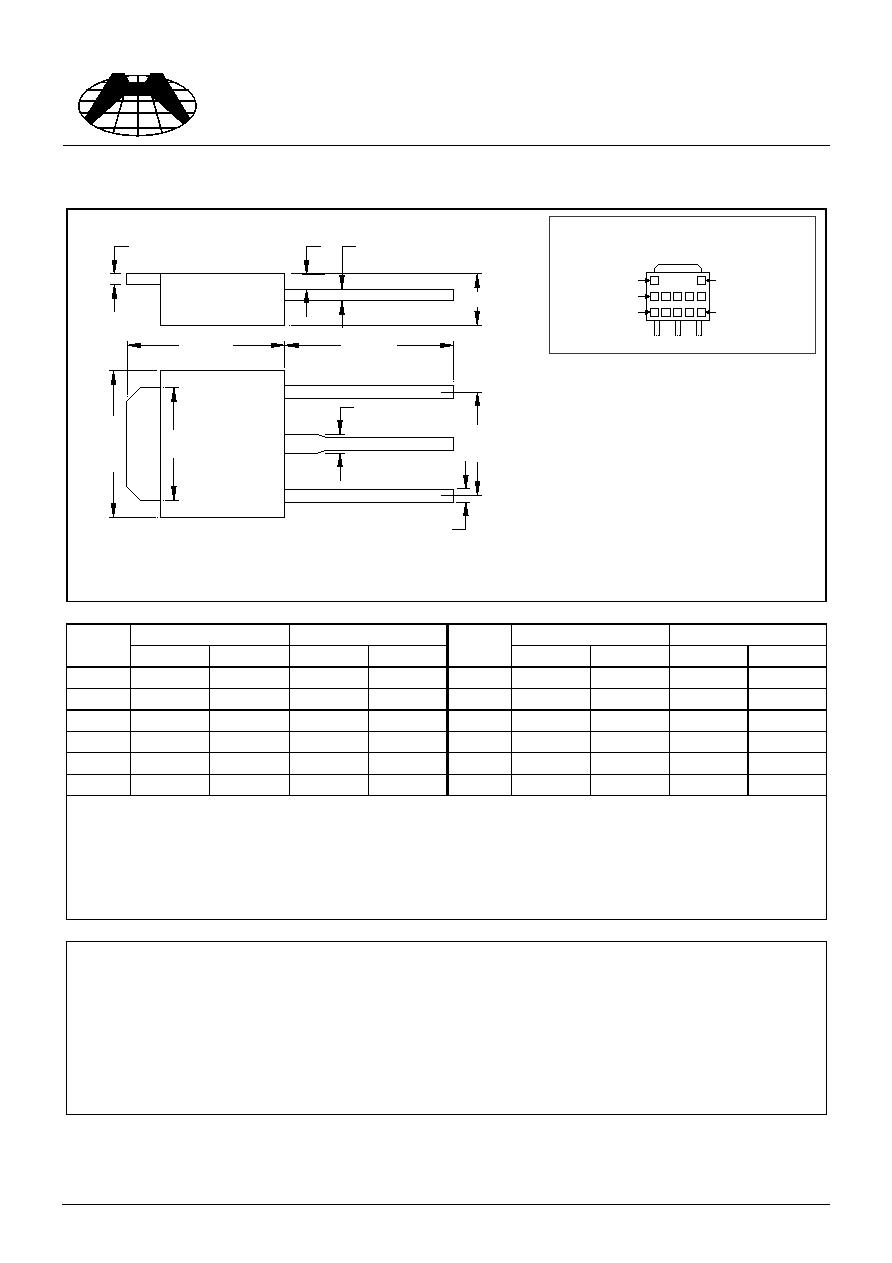
TO-251 Dimension
*:Typical
Inches
Millimeters
Inches
Millimeters
DIM
Min.
Max.
Min.
Max.
DIM
Min.
Max.
Min.
Max.
A
0.0177
0.0217
0.45
0.55
G
0.2559
-
6.50
-
B
0.0354
0.0591
0.90
1.50
H
-
*0.1811
-
*4.60
C
0.0177
0.0236
0.45
0.60
I
-
0.0354
-
0.90
D
0.0866
0.0945
2.20
2.40
J
-
0.0315
-
0.80
E
0.2520
0.2677
6.40
6.80
K
0.2047
0.2165
5.20
5.50
F
0.2677
0.2835
6.80
7.20
Notes :
1.Dimension and tolerance based on our Spec. dated May. 24,1995.
2.Controlling dimension : millimeters.
3.Maximum lead thickness includes lead finish thickness, and minimum lead thickness is the minimum thickness of base material.
4.If there is any question with packing specification or packing method, please contact your local HSMC sales office.
Material :
∑
Lead : 42 Alloy ; solder plating
∑
Mold Compound : Epoxy resin family, flammability solid burning class:UL94V-0
Important Notice:
∑
All rights are reserved. Reproduction in whole or in part is prohibited without the prior written approval of HSMC.
∑
HSMC reserves the right to make changes to its products without notice.
∑
HSMC semiconductor products are not warranted to be suitable for use in Life-Support Applications, or systems.
∑
HSMC assumes no liability for any consequence of customer product design, infringement of patents, or application assistance.
Head Office And Factory :
∑
Head Office (Hi-Sincerity Microelectronics Corp.) : 10F.,No. 61, Sec. 2, Chung-Shan N. Rd. Taipei Taiwan R.O.C.
Tel : 886-2-25212056 Fax : 886-2-25632712, 25368454
∑
Factory 1 : No. 38, Kuang Fu S. Rd., Fu-Kou Hsin-Chu Industrial Park Hsin-Chu Taiwan. R.O.C
Tel : 886-3-5983621~5 Fax : 886-3-5982931
A
E
F
G
H
J
I
3
2
1
K
C
D
B
Style : Pin 1.Vin 2.Ground 3.Vout
3-Lead TO-251 Plastic Package
HSMC Package Code : I
Marking :
HSMC Logo
Part Number
Date Code
Product Series
Rank
Ink Mark