 | –≠–ª–µ–∫—Ç—Ä–æ–Ω–Ω—ã–π –∫–æ–º–ø–æ–Ω–µ–Ω—Ç: HMJE13001 | –°–∫–∞—á–∞—Ç—å:  PDF PDF  ZIP ZIP |
HI-SINCERITY
MICROELECTRONICS CORP.
Spec. No. : HA200213
Issued Date : 2002.06.01
Revised Date : 2005.02.05
Page No. : 1/4
HMJE13001
HSMC Product Specification
HMJE13001
NPN Triple Diffused Planar Type High Voltage Transistor
Description
The HMJE13001 is a medium power transistor designed for use in switching
applications.
Features
∑
High breakdown voltage
∑
Low collector saturation voltage
∑
Fast switching speed
Absolute Maximum Ratings
∑
Maximum Temperatures
Storage Temperature ........................................................................................................................... -55 ~ +150
∞
C
Junction Temperature .................................................................................................................................... +150
∞
C
∑
Maximum Power Dissipation
Total Power Dissipation (T
A
=25
∞
C) ...................................................................................................................... 1 W
Total Power Dissipation (T
C
=25
∞
C) .................................................................................................................... 10 W
∑
Maximum Voltages and Currents
BV
CBO
Collector to Base Voltage....................................................................................................................... 600 V
BV
CEO
Collector to Emitter Voltage.................................................................................................................... 400 V
BV
EBO
Emitter to Base Voltage.............................................................................................................................. 6 V
I
C
Collector Current (DC)................................................................................................................................ 300 mA
I
C
Collector Current (Pulse)............................................................................................................................ 600 mA
I
B
Base Current (DC)........................................................................................................................................ 40 mA
I
B
Base Current (Pulse).................................................................................................................................. 100 mA
Electrical Characteristics
(T
A
=25
∞
C)
Symbol
Min.
Typ.
Max.
Unit
Test Conditions
BV
CBO
600
-
-
V
I
C
=100uA
BV
CEO
400
-
-
V
I
C
=10mA
BV
EBO
6
-
-
V
I
E
=10uA
I
CBO
-
-
10
uA
V
CB
=550V
I
CEO
-
-
10
uA
V
CB
=400V
I
EBO
-
-
10
uA
V
EB
=6V
*V
CE(sat)1
-
-
400
mV
I
C
=50mA, I
B
=10mA
*V
CE(sat)2
-
-
750
mV
I
C
=100mA, I
B
=20mA
*V
BE(sat)
-
-
1
V
I
C
=50mA, I
B
=10mA
*h
FE1
8
-
-
V
CE
=10V, I
C
=10mA
*h
FE2
10
-
36
V
CE
=10V, I
C
=50mA
*Pulse Test: Pulse Width
380us, Duty Cycle
2%
TO-92
HI-SINCERITY
MICROELECTRONICS CORP.
Spec. No. : HA200213
Issued Date : 2002.06.01
Revised Date : 2005.02.05
Page No. : 2/4
HMJE13001
HSMC Product Specification
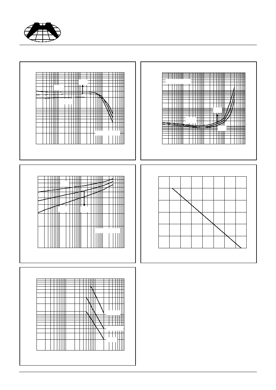
Characteristics Curve
Power Derating
0
200
400
600
800
1000
1200
0
20
40
60
80
100
120
140
160
Ta(
o
C), Ambtient Temperatuer
P
D
(
m
W
)
,
P
ow
er
D
i
s
s
i
pat
i
o
n
Safe Operating Area
0.01
0.1
1
1
10
100
1000
Forward Voltage-V
CE
(V)
Co
lle
c
t
o
r
Cu
r
r
e
n
t
-
I
C
(A
)
PT=1mS
PT=100mS
PT=1S
Current Gain & Collector Current
1
10
100
0.1
1
10
100
1000
Collector Current-I
C
(mA)
hFE
25
o
C
75
o
C
125
o
C
hFE @ V
CE
=10V
Saturation Voltage & Collector Current
10
100
1000
10000
100000
0.1
1
10
100
1000
Collector Current-I
C
(mA)
S
a
tu
r
a
ti
o
n
V
o
l
t
a
g
e
(
m
V
)
125
o
C
75
o
C
25
o
C
V
CE(sat)
@ I
C
=5I
B
Saturation Voltage & Collector Current
100
1000
0.1
1
10
100
1000
Collector Current-I
C
(mA)
S
a
tu
r
a
ti
o
n
V
o
l
t
a
g
e
(
m
V
)
25
o
C
75
o
C
125
o
C
V
BE(sat)
@ I
C
=5I
B
HI-SINCERITY
MICROELECTRONICS CORP.
Spec. No. : HA200213
Issued Date : 2002.06.01
Revised Date : 2005.02.05
Page No. : 3/4
HMJE13001
HSMC Product Specification
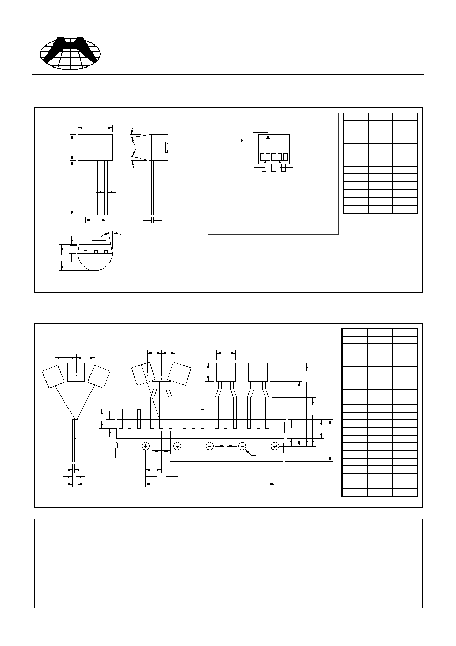
TO-92 Dimension
TO-92 Taping Dimension
Important Notice:
∑
All rights are reserved. Reproduction in whole or in part is prohibited without the prior written approval of HSMC.
∑
HSMC reserves the right to make changes to its products without notice.
∑
HSMC semiconductor products are not warranted to be suitable for use in Life-Support Applications, or systems.
∑
HSMC assumes no liability for any consequence of customer product design, infringement of patents, or application assistance.
Head Office And Factory:
∑
Head Office (Hi-Sincerity Microelectronics Corp.): 10F.,No. 61, Sec. 2, Chung-Shan N. Rd. Taipei Taiwan R.O.C.
Tel: 886-2-25212056 Fax: 886-2-25632712, 25368454
∑
Factory 1: No. 38, Kuang Fu S. Rd., Fu-Kou Hsin-Chu Industrial Park Hsin-Chu Taiwan. R.O.C
Tel: 886-3-5983621~5 Fax: 886-3-5982931
3
1
A
D
B
C
I
1
E
2
3
G
H
2
F
H2A
H2A
H2
H2
D2
A
H
W
W1
H3
H4
H1
L1
L
P2
P
P1
F1F2
D1
D
T2
T
T1
DIM
Min.
Max.
A
4.33
4.83
B
4.33
4.83
C
12.70
-
D
0.36
0.56
E
-
*1.27
F
3.36
3.76
G
0.36
0.56
H
-
*2.54
I
-
*1.27
1
-
*5
∞
2
-
*2
∞
3
-
*2
∞
*: Typical, Unit: mm
3-Lead TO-92 Plastic Package
HSMC Package Code: A
DIM
Min.
Max.
A
4.33
4.83
D
3.80
4.20
D1
0.36
0.53
D2
4.33
4.83
F1,F2
2.40
2.90
H
15.50
16.50
H1
8.50
9.50
H2
-
1
H2A
-
1
H3
-
27
H4
-
21
L
-
11
L1
2.50
-
P
12.50
12.90
P1
5.95
6.75
P2
50.30
51.30
T
-
0.55
T1
-
1.42
T2
0.36
0.68
W
17.50
19.00
W1
5.00
7.00
Unit: mm
Marking:
Pb Free Mark
Pb-Free: "
.
"
(Note)
Normal: None
Control Code
Date Code
H
1 3 0
E
0
J
1
M
Note: Green label is used for pb-free packing
Pin Style: 1.Emitter 2.Collector 3.Base
Material:
∑
Lead solder plating: Sn60/Pb40 (Normal),
Sn/3.0Ag/0.5Cu or Pure-Tin (Pb-free)
∑
Mold Compound: Epoxy resin family,
flammability solid burning class: UL94V-0
HI-SINCERITY
MICROELECTRONICS CORP.
Spec. No. : HA200213
Issued Date : 2002.06.01
Revised Date : 2005.02.05
Page No. : 4/4
HMJE13001
HSMC Product Specification
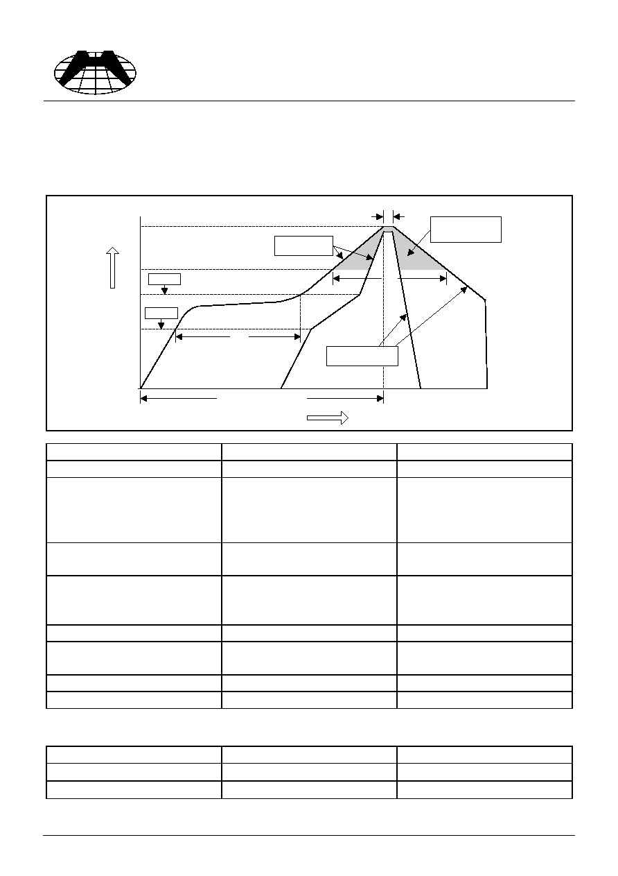
Soldering Methods for HSMC's Products
1. Storage environment: Temperature=10
o
C~35
o
C Humidity=65%±15%
2. Reflow soldering of surface-mount devices
Profile Feature
Sn-Pb Eutectic Assembly
Pb-Free Assembly
Average ramp-up rate (T
L
to T
P
)
<3
o
C/sec
<3
o
C/sec
Preheat
- Temperature Min (Ts
min
)
- Temperature Max (Ts
max
)
- Time (min to max) (ts)
100
o
C
150
o
C
60~120 sec
150
o
C
200
o
C
60~180 sec
Tsmax to T
L
- Ramp-up Rate
<3
o
C/sec
<3
o
C/sec
Time maintained above:
- Temperature (T
L
)
- Time (t
L
)
183
o
C
60~150 sec
217
o
C
60~150 sec
Peak Temperature (T
P
)
240
o
C +0/-5
o
C
260
o
C +0/-5
o
C
Time within 5
o
C of actual Peak
Temperature (t
P
)
10~30 sec
20~40 sec
Ramp-down Rate
<6
o
C/sec
<6
o
C/sec
Time 25
o
C to Peak Temperature
<6 minutes
<8 minutes
3. Flow (wave) soldering (solder dipping)
Products
Peak temperature
Dipping time
Pb devices.
245
o
C
±
5
o
C
5sec
±
1sec
Pb-Free devices.
260
o
C +0/-5
o
C
5sec
±
1sec
Figure 1: Temperature profile
t
P
t
L
Ramp-down
Ramp-up
Ts
max
Ts
min
Critical Zone
T
L
to T
P
t
S
Preheat
T
L
T
P
25
t 25
o
C to Peak
Time
Tem
p
erature