GM16C550
ASYNCHRONOUS COMMUNICATIONS
ELEMENT WITH FIFOs
Version 1.0
Descriptions
The GM16C550 is an asynchronous communi-
cations element (ACE) that is functionally equivalent
to the GM16C450, and addition-ally incorporates a
16byte FIFOs are available on both the transmitter
and receiver, and can be activated by placing the
device in the FIFO mode. After a reset, the registers
of the GM16C550 are identical to those of the
GM16C450.
The UART performs serial-to-parallel conversion on
data characters received from a peripheral device or
a MODEM, and parallel-to- serial conversion on
data characters received from the CPU. The CPU
can read the complete status of the UART at any
time during the functional operation. Status
information reported includes the type and condition
of the transfer operations being performed by
the UART, as well as any error conditions (parity,
overrun, framing, or break interrupt).
Features
Device Code Name
D0
D1
D2
D3
D4
D5
D6
D7
RCLK
SIN
SOUT
CS0
CS1
-CS2
-BAUDQUT
XTAL1
XTAL2
-DOSTR
DOSTR
VSS
VCC
RI-
DCD-
DSR-
CTS-
MR
OUT1-
DTR-
RTS-
OUT2-
INTRPT
RXRDY-
A0
A1
A2
ADS-
TXRDY-
DDIS-
DISTR
DISTR-
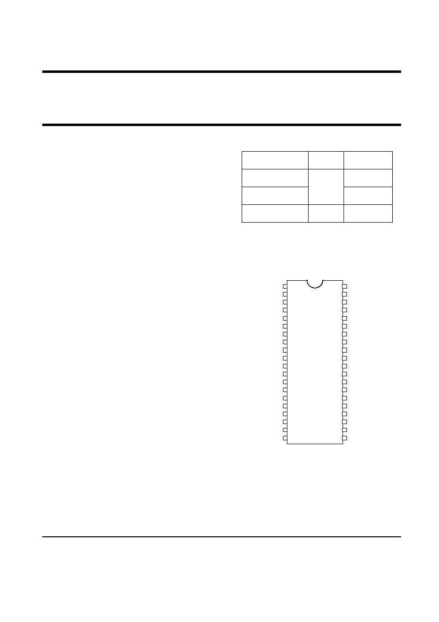
40DIP
Pin Configuration
1
�
Compatible to the Industry Standard 16C550
�
Modem control signals include CTS, RTS,DSR
DTR, RI and DCD
�
Programmable serial characteristics :
- 5-, 6-, 7- or 8-bit characters
- Even-, odd-, or no-parity bit generation and
detection
- 1-, 11/2- or 2-stop bit generation
- Baud rate generation (DC to 256K baud)
�
16 byte FIFO reduces CPU interrupts.
�
Independent control of transmit, receive, line
status, data set interrupts, FIFOs.
�
Full status reporting capabilities
�
Three-state, TTL drive capabilities for bi-directional
data bus and control bus.
�
40DIP/44PLCC/48LQFP
GM16C550
GM16C550-44
GM16C550-48
Part Number
Voltage
PKG
40 DIP
5V
44 PLCC
3.3V
48 LQFP

�
�
�
�
�
�
8
389(
�

�
�
&%6
& 2&
.*&
& �&
&)&:*
/&:
+:2+:
/&
;
<*%'%/
&%*+
&%%%
%'%%&!%
%
���
=& >2&$:=:' ?@A+A:' ?$:=:/&!%
()#*+
�
,-
.
/
�
/
0
()#*12
3
((
((
#*+
�
#*12
3
3
((
3
((
4*+
#
5
6
#
5776
4*12
3
#
5
6
3
#
5776
869 6:+,**-
8((9
�
6
((5�
3�
�
#
#*)
'
6
((5�
3�
�;
5
5;
��
3�
'
#
())
'
6
'
#
)
'3
5;
��
3�
'3
6
<,(2
3
3
3
<,(2
���
=5& :=: =:
,-
.
=-*
/
0
>#
()#**((
%(51?
�
3
*%
>40=
()4**((
0.*
3
*%
#
#**((
<.
*%
40=
4**((
3
*%

GM16C550
4
AC Characteristics
C
0
T
A
�
=
to V/3.3V
5
V
,
C
70
CC
=
�
+
Symbol
Parameter
Min Max Units
Conditions
ADS
t
Address Srobe Width
60
ns
AH
t
Address Hold Time
0
ns
AR
t
RD
,
RD
Delay from Address
30
ns
Note 1
AS
t
Address Setup Time
60
ns
AW
t
WR
,
WR
Delay from Select
30
ns
Note 1
CH
t
Chip Select Hold Time
0
ns
CS
t
Chip Select Setup time
60
ns
CSR
t
RD
,
RD
Delay from Chip Select
30
ns
Note 1
CSW
t
WR
,
WR
Delay from Select
30
ns
Note 1
DH
t
Data Hold Time
30
ns
DS
t
Date Setup Time
30
ns
HZ
t
RD
,
RD
to Floating Data Delay
0
100
ns
100 pF loading, Note 3
MR
t
Master Reset Pulse Width
5
ns
RA
r
Address Hold Time from
RD
,
RD
20
ns
Note 1
RC
t
Read Cycle Delay
125
ns
RCS
t
Chip Select Hold Time from
RD
,
RD
20
ns
Note 1
RD
t
RD
,
RD
Strobe Width
125
ns
RDD
t
RD
,
RD
to Driver Enable/Disable
60
ns
100 pF loading, Note 3
RVD
t
Delay from -
RD
,
RD
to Data
125
ns
100 pF loading,
WA
t
Address Hold Time from
WR
,
WR
20
ns
Note 1
WC
t
Write Cycle Delay
150
ns
WCA
t
Chip Select Hold Time from
WR
,
WR
20
ns
Note 1
WR
t
WR
,
WR
Strobe Width
100
ns
XH
t
Duration of clock High Pulse
55
ns
External Clock (8.0 MHz Max.)
XL
t
Duration of clock Low Pulse
55
ns
Exrternal Clock (8.9 MHz Max.)
RC
Read Cycle=
RC
RD
AR
t
t
t
+
+
280
ns
Note 4
WC
Write Cycle=
WC
WR
AW
t
t
t
+
+
280
ns
Baud Generator
N
Baud Divisor
1
16
2
-1
BHD
t
Baud Output Positive Edge Delay
175
ns
100 pF load
BLD
t
Baud Output Negative Edge Delay
175
ns
100 pF load
HW
t
Baud Output Up Time
75
ns
MHz
0
.
8
f
X
=
, +2, 100 pF load
LW
t
Baud Output Down Time
100
ns
MHz
0
.
8
f
X
=
, +2, 100 pF load

GM16C550
5
AC Characteristics
C
0
T
A
�
=
to
C
70
�
+
,
V/3.3V
5
V
CC
=
Symbol Parameter Min Max Units Conditions
Receiver
RINT
t
Delay from
RD
,
RD
(RD RBR/ or
RD LSR) to Reset Interupt
1
s
�
100 pF load
SCD
t
Delay from RCLK to Sample Time
2
s
�
SINT
t
Delay from Stop to Set Interrupt
1
RCLK
Cycles
Note 2
Transmitter
HR
t
Delay from
WR
,
WR
(WR THR)
To Reset Interrupt
175
ns
100 pF load
IR
t
Delay from
RD
,
RD
(RD IIR)
To Reset Interrupt (THRE)
250
ns
100 pF load
IRS
t
Delay from Initial INTR Reset
To Transmit Start
8
24
Baudout
Cycles
SI
t
Delay from Initial Write to Interrupt
16
24
Baudout
Cycles
Note 5
STI
t
Delay from Stop to Interrupt (THRE)
8
8
Baudout
Cycles
Note 5
SXV
t
Delay from Start to TXRDY Active
8
Baudout
Cycles
100 pF load
WXI
t
Delay from Write to TXRDY inactive
195
ns
100 pF load
Modem Control
MDO
t
Delay from
WR
,
WR
(WR MCR) to Output
200
ns
100 pF load
RIM
t
Delay to Reset Interrupt from
RD
,
RD
(RD MSR)
250
ns
100 pF load
SIM
t
Delay to Set Interrupt from MODEM Input
250
ns
100 pF load
Notes
1. Applicable only when ADS is tied low.
2. In the FIFO mode (FCRO=1) the trigger level interrupts, the receiver data available indication, the active RXRDY indica-tion
and the overrun error indication will be delayed 3 RCLKs. Status indicators (PE, FE, BI) will be delayed 3 RCLKs after the first
byte has been received. For subsequently received bytes these indicators will be updated immediately after RDRBR goes
inactive. Timeout interrupt is delayed 8 RCLKs.
3. Change and discharge time is determined by VOL, VOH and the external loading.
4.In FIFO mode RC=425 ns (minimum) between reads of the receiver FIFO and the status registers (interrupt identifica- tion
register or line status register).
5. This delay will be lengthened by 1 character time, minus the last stop bit time if the transmitter interrupt delay circuit is active
(See FIFO Interrupt Mode Operatione)