T h e G M 7 1 C ( S ) 1 8 1 6 0 C /C L i s t h e n e w
generation dynamic RAM organized 1,048,576
x 16 bit. GM71C(S)18160C/CL has realized
higher density, higher performance and various
functions by utilizing advanced CMOS process
technology. The GM71C(S)18160C/CL offers
Fast Page Mode as a high speed access mode.
M u l t i p l e x e d a d d r e s s i n p u t s p e r m i t t h e
G M 7 1 C ( S ) 1 8 1 6 0 C /C L t o b e p a c k a g e d i n
s t a n d a r d 4 0 0 m i l 4 2 p i n p l a s t i c S O J , a n d
standard 400mil 44(50)pin plastic TSOP II. The
package size provides high system bit densities
a n d i s c o m p a t i b l e w i t h w i d e l y a v a i l a b l e
automated testing and insertion equipment.
Description
F eatur es
* 1 ,048,576 Words x 16 Bit Organization
* Fast Page Mode Capability
* S ingle Power Supply (5V+/-10%)
* Fast Access Time & Cycle Time
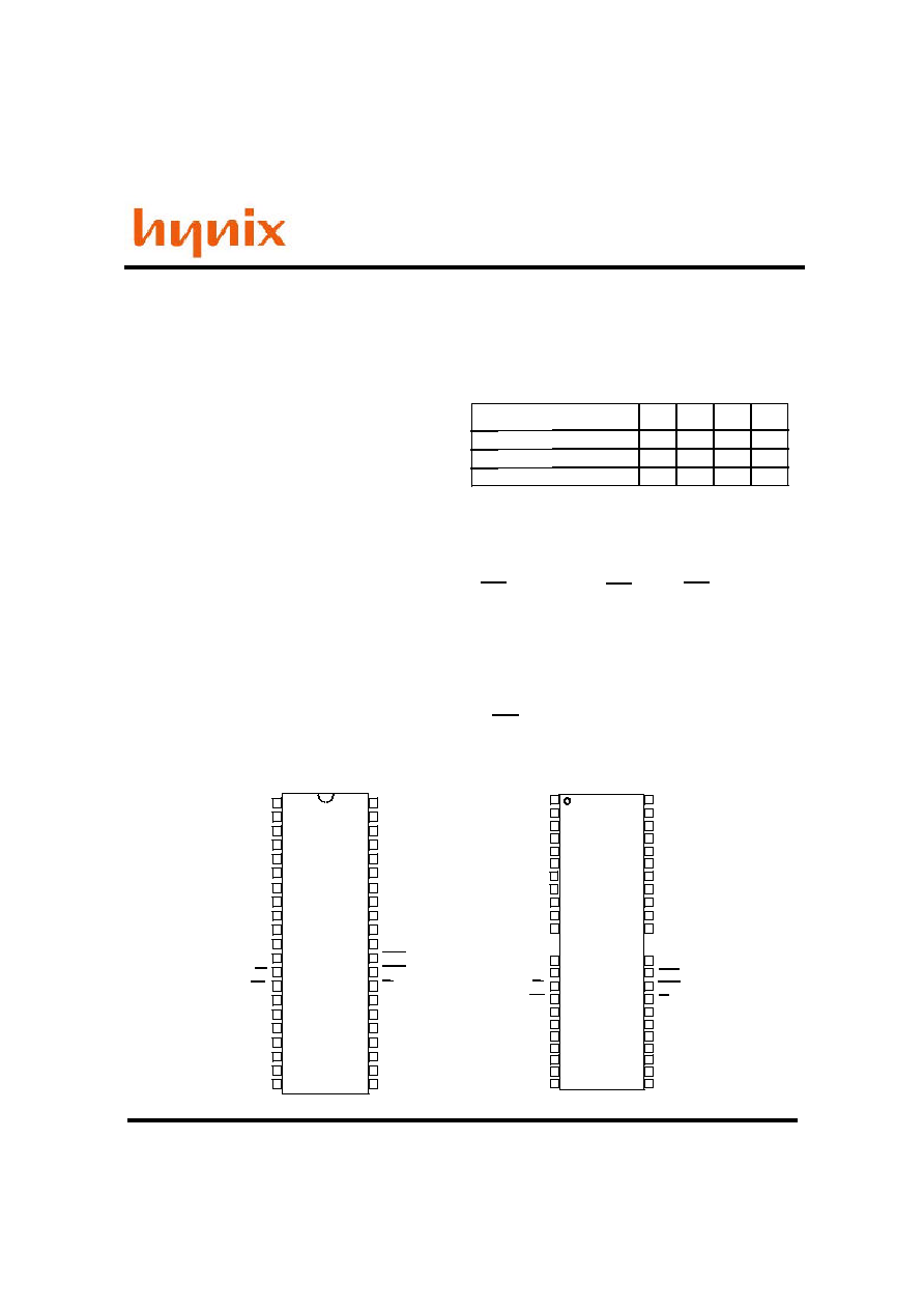
P in Configuration
1,048,576 WORDS x 16 BIT
CMOS DYNAMIC RAM
GM71CS18160CL
(Unit: ns)
G M 7 1 C ( S ) 1 8 1 6 0 C /C L - 5
G M 7 1 C ( S ) 1 8 1 6 0 C /C L - 6
G M 7 1 C ( S ) 1 8 1 6 0 C /C L - 7
t
R A C
t
C A C
t
R C
t
P C
50
60
13
15
9 0
1 1 0
35
40
70
18
1 3 0
45
* Low Power
Active : 1045/935/825mW (MAX )
S tandby : 11mW (CMOS level : MAX )
0.83mW (L-version : MAX )
* R A S O nly Refresh, CAS before RAS Refresh,
Hidden Refresh Capability
* All inputs and outputs TTL Compatible
* 1024 Refresh Cycles/16ms
* 1024 Refresh Cycles/128ms (L-version)
* Self Refresh Operation (L-version)
* B attery B ack Up Operation (L-version)
* 2 CAS byte Control
(Top View)
GM71C18160C
4 2
4 3
4 4
4 5
4 6
4 0
4 1
3 3
3 0
3 1
3 2
2 7
2 8
2 9
2 6
3 4
3 5
3 6
4 7
4 8
4 9
5 0
NC
NC
V
S S
I/O 1 5
I/O 1 4
I/O 1 3
I/O 1 2
I/O 1 1
I/O 1 0
I/O 9
I/O 8
V
S S
L C A S
U C A S
O E
A 8
A 7
A 6
A 5
A 4
V
S S
A 9
V
S S
I/O 1 5
I/O 1 4
I/O 1 3
I/O 1 2
3 8
3 9
4 0
4 1
4 2
I/O 1 1
I/O 1 0
I/O 9
I/O 8
NC
3 2
3 3
3 4
3 5
3 6
V
S S
3 7
L C A S
U C A S
O E
2 9
3 0
3 1
A 9
A 8
A 7
2 6
2 7
2 8
A 6
A 5
A 4
2 3
2 4
2 5
V
S S
2 2
1 1
1
2
3
4
5
7
8
9
1 0
6
1 5
1 6
1 7
1 8
1 9
2 0
2 1
2 2
2 3
2 4
2 5
NC
NC
I/O 0
I/O 1
I/O 2
I/O 3
I/O 4
I/O 5
I/O 6
I/O 7
V
C C
NC
W E
R A S
A 1 1
A 1 0
A 0
A 1
V
C C
V
C C
A 2
A 3
44(50) TSOP II
V
C C
I/O 0
I/O 1
I/O 2
I/O 3
1
2
3
4
5
I/O 4
I/O 5
I/O 6
I/O 7
NC
7
8
9
1 0
1 1
V
C C
6
NC
W E
R A S
1 2
1 3
1 4
NC
NC
A 0
1 5
1 6
1 7
A 1
A 2
A 3
1 8
1 9
2 0
V
C C
2 1
42 SOJ
Rev 0.1 / Apr'01

GM71CS18160CL
GM71C18160C
Rev 0.1 / Apr'01
P in Descr iption
P in
F unction
P in
F unction
A0-A9
A0-A9
I/O0-I/O 1 5
R A S
W E
V
C C
V
S S
NC
Address Inputs
Refresh Address Inputs
Data-In/Out
Row Address Strobe
Read/W rite Enable
Power (+5V)
Ground
No Connection
Ordering Information
U C A S , L C A S
Column Address Strobe
O E
Output Enable
Absolute Maximum Ratings*
P
D
1.0
Power Dissipation
W
Note: Operation at or above Absolute Maximum Ratings can adversely affect device reliability.
Symbol
Parameter
Rating
Unit
T
A
T
S T G
V
IN/O U T
V
C C
I
O U T
0 ~
+
70
-55 ~
+
1 2 5
50
Ambient Temperature under B ias
S torage Temperature (Plastic)
Voltage on any Pin Relative to V
S S
Voltage on V
C C
Relative to V
S S
Short Circuit Output Current
C
C
V
V
mA
-1.0 ~
+
7.0V
-1.0 ~
+
7.0V
T ype No.
Access Time
Package
G M 7 1 C ( S ) 1 8 1 6 0 C J /C L J - 5
G M 7 1 C ( S ) 1 8 1 6 0 C J /C L J - 6
G M 7 1 C ( S ) 1 8 1 6 0 C J /C L J - 7
50ns
60ns
70ns
4 0 0 Mil
42 Pin
Plastic SOJ
50ns
60ns
70ns
4 0 0 Mil
44(50) Pin
Plastic TSOP II
G M 7 1 C ( S ) 1 8 1 6 0 C T /C L T - 5
G M 7 1 C ( S ) 1 8 1 6 0 C T /C L T - 6
G M 7 1 C ( S ) 1 8 1 6 0 C T /C L T - 7

GM71CS18160CL
GM71C18160C
Rev 0.1 / Apr'01
T r uth Table
Notes: 1. H: High (inactive) L: Low(active) D: H or L
2.
t
W C S
>= 0ns Early write cycle
t
W C S
<= 0ns Delayed write cycle
3. Mode is determined by the OR function of the UCAS and LCAS. (Mode is set by earliest of
UCAS and LCAS active edge and reset by the latest of UCAS and LCAS inactive edge.) However
write OPERATION and output High-Z control are done independently by each UCAS,LCAS.
ex) if RAS = H to L, UCAS = H, LCAS = L, then CAS-before-RAS refresh cycle is selected.
H
L
L
L
D
H
L
H
D
H
H
L
D
H
H
H
D
D
L
L
Output
Open
Valid
Valid
Valid
Lower byte
Upper byte
Word
Operation
S tandby
RAS-only
Refresh cycle
Read cycle
L
L
L
L
L
L
H
L
H
Early write cycle
L
H
L
L
H
Open
Open
Open
L
L
L
L
Undefined
Delayed Write
cycle
L
L
L
H
H
H to L
L
C B R R e f resh
or
Self Refresh
(L-series)
H to L
H
L
H to L
L
L
RAS
L C A S
UCAS
W E
O E
Notes
1,3
1,3
1,3
1,3
1,3
1,2,3
1,2,3
1,3
Lower byte
Upper byte
Word
Lower byte
Upper byte
Word
Lower byte
Upper byte
Word
Undefined
Undefined
Open
Open
Open
Open
Open
Valid
Valid
Valid
Word
Word
Word
Word
Read-modify
-write cycle
Read cycle
(Output disabled)
D
D
H to L
H to L
H to L
L
L
L
L
L
L
L
H
L
L
L
L
H
D
D
L
H
H
H
H
L
D
D
D
D
D
D
L to H
L to H
L to H
L
L
L
L
R ecommended DC Operating Conditions
(T
A
= 0 ~
+
70C)
Symbol
Parameter
Unit
V
C C
V
IH
V
I L
S upply Voltage
Input High Voltage
Input Low Voltage
V
V
V
M a x
5.5
6.0
0.8
T yp
5.0
-
-
M in
4.5
2.4
-1.0
Note: All voltage referred to V ss.
T he supply voltage with all VCC pins must be on the same level. The supply voltage with all VSS pins must be
on the same level.

GM71CS18160CL
GM71C18160C
Rev 0.1 / Apr'01
DC Electrical Characteristics
(V
C C
= 5V+/-10%, V ss = 0V, T
A
= 0 ~ 70C)
Symbol
Parameter
Note
V
O H
V
O L
Output Level
Output "H" Level Voltage (I
O U T
=
-5mA
)
Unit
M a x
V
C C
0.4
M in
2.4
0
Output Level
Output "L" Level Voltage (I
O U T
=
4.
2m A )
I
C C 1
Operating Current
Average Power Supply Operating Current
(RAS, UCAS or LCAS Cycling
:
t
R C
=
t
R C
min)
I
C C 2
S tandby Current (TTL)
Power Supply Standby Current
( R A S , U C A S , L C A S = V
IH
,
D
O U T
=
High-Z)
2
-
I
C C 3
RAS Only Refresh Current
Average Power Supply Current
RAS Only Refresh Mode
(t
R C
=
t
R C
min)
I
C C 4
I
C C 5
S tandby Current (CMOS)
Power Supply Standby Current
( R A S , U C A S o r L C A S > = V
CC
- 0.2V, D
O U T
= High-Z)
1
-
I
C C 6
CAS-before-RAS Refresh Current
(t
R C
=
t
R C
min)
1 5 0
-
I
L(I)
10
-10
I
L ( O )
10
-10
Input Leakage Current
Any Input (0V
<=
V
IN
<=
6 V )
Output Leakage Current
(D
O U T
is Disabled, 0V
<=
V
O U T
<=
6 V )
Fast Page Mode Current
Average Power Supply Current
Fast Page Mode
(t
P C
= t
P C
min)
1 9 0
-
50ns
60ns
70ns
1 7 0
1 5 0
-
-
-
1 9 0
-
50ns
60ns
70ns
1 7 0
1 5 0
-
-
1 8 5
-
50ns
60ns
70ns
1 6 5
1 4 5
-
1 9 0
-
50ns
60ns
70ns
-
-
1 7 0
1 5 0
I
C C 7
I
C C 8
I
C C 9
Self-Refresh Mode Current
( R A S , U C A S o r L C A S < = 0 . 2 V
,
D
O U T
=
High-Z)
3 0 0
-
Note: 1. I
C C
depends on output load condition when the device is selected.
I
C C
(max) is specified at the output open condition.
2. Address can be changed once or less while RAS = V
I L
.
3. Address can be changed once or less while LCAS and UCAS = V
IH
.
4. UCAS = L (<=0.2) and LCAS = L (<=0.2) while RAS = L (<=0.2).
5. L-version.
V
V
mA
mA
uA
uA
uA
mA
1, 2
mA
2
mA
1, 3
mA
5
-
S tandby Current RAS = V
IH
U
C A S , L C A S = V
I L
D
O U T
=
Enable
mA
1
B attery B ack Up Operating Current
(Standby with CBR Refresh)
(t
R C
=125us
,
t
R A S
<=
0.3
us,
D
O U T
=
High-Z)
5 0 0
-
4,5
uA
uA
5
5
GM71CS18160CL
GM71C18160C
Rev 0.1 / Apr'01
R ead, W r ite, Read-Modify-W r ite and Refr esh Cycles
(Common Parameters)
Capacitance
(V
CC
= 5V+/-10%, T
A
= 25C)
Symbol
Parameter
Note
C
I1
C
I2
C
I/O
Input Capacitance (Address)
Input Capacitance (Clocks)
Output Capacitance (Data-In/Out)
1
1
1, 2
Unit
pF
pF
pF
M a x
5
7
7
M in
-
-
-
AC Characteristics
(V
C C
= 5V+/-10%, T
A
= 0 ~
+
70C, Note 1, 2, 18)
Test Conditions
Input rise and fall times : 5 ns
Output timing reference levels : 0.4V, 2.4V
Input timing reference levels : 0.8V , 2.4V
Output load : 2TTL gate + C
L
(100 pF )
(Including scope and jig)
Symbol
Parameter
Note
Max
Unit
Min
Max
Min
Max
Min
t
R C
Random Read or Write Cycle Time
9 0
-
1 1 0
-
1 3 0
-
t
R P
R A S Precharge Time
30
-
40
-
50
-
t
R A S
RAS Pulse Width
50
10,000
60
10,000
70
10,000
t
C A S
CAS Pulse Width
10,000
10,000
10,000
15
18
t
A S R
Row Address Set up Time
0
-
-
-
0
0
t
R A H
Row Address Hold Time
7
-
-
-
10
10
t
A S C
Column Address Set-up Time
0
-
-
-
0
0
t
C A H
Column Address Hold Time
-
-
-
10
15
t
R C D
RAS to CAS Delay Time
17
45
45
52
20
20
3
t
R A D
RAS to Column Address Delay Time
12
30
30
35
15
15
4
t
R S H
RAS Hold Time
13
-
-
-
15
18
t
C S H
CAS Hold Time
50
-
-
-
60
70
t
C R P
C A S t o R A S Precharge Time
5
-
-
-
5
5
t
T
T ransition Time (Rise and Fall)
3
50
50
50
3
3
7
t
D Z O
OE Delay Time from D
IN
0
-
-
-
0
0
t
DZC
CAS Delay Time from D
IN
0
-
-
-
0
0
G M 7 1 C ( S ) 1 8 1 6 0
C / C L - 5
OE to D
IN
Delay Time
13
-
-
-
15
18
5
6
6
t
C P
C A S Precharge Time
7
-
10
-
10
-
t
O D D
G M 7 1 C ( S ) 1 8 1 6 0
C / C L - 6
G M 7 1 C ( S ) 1 8 1 6 0
C / C L - 7
ns
ns
ns
ns
ns
ns
ns
ns
ns
ns
ns
ns
ns
ns
ns
ns
ns
ns
13
7
Note: 1. Capacitance measured with B oonton Meter or effective capacitance measuring method.
2. UCAS and LCAS = V
IH
to disable D
O U T
.
24
21
21
22
23
GM71CS18160CL
GM71C18160C
Rev 0.1 / Apr'01
R ead Cycle
W r ite Cycle
Symbol
Parameter
Note
Max
Unit
Min
Max
Min
t
R A C
-
60
-
70
t
C A C
-
15
-
18
t
A A
-
30
-
35
t
R C S
0
-
0
-
t
R C H
0
-
-
0
8,9
9,10,17
9,11,17
-
15
-
18
9,25
12,22
G M 7 1 C ( S ) 1 8 1 6 0
C / C L - 6
t
O A C
G M 7 1 C ( S ) 1 8 1 6 0
C / C L - 7
t
R R H
5
-
-
5
12
t
R A L
30
-
-
35
t
O F F
15
15
13
-
-
t
C A L
30
-
-
35
t
C L Z
0
-
-
0
t
O E Z
15
15
13
-
-
t
OH
3
-
-
3
t
OHO
3
-
-
3
t
C D D
15
-
-
18
Access Time from RAS
Access Time from CAS
Access Time from Address
Read Command Setup Time
Read Command Hold Time to CAS
Access Time from OE
Read Command Hold Time to RAS
Column Address to RAS Lead Time
Output B uffer Turn-off Time
Column Address to CAS Lead Time
CAS to Output in Low-Z
Output B uffer Turn-off Time to OE
Output Data Hold Time
Output Data Hold Time from OE
CAS to D
IN
Delay Time
5
Max
Min
-
50
-
13
-
25
0
-
0
-
-
13
G M 7 1 C ( S ) 1 8 1 6 0
C / C L - 5
5
-
25
-
13
-
25
-
0
-
13
-
3
-
3
-
13
-
ns
ns
ns
ns
ns
ns
ns
ns
ns
ns
ns
ns
ns
ns
ns
Symbol
Parameter
Note
Max
Unit
Min
Max
Min
t
W C S
0
-
0
-
t
W C H
10
-
15
-
t
W P
10
-
10
-
t
R W L
15
-
18
-
t
C W L
15
-
-
18
t
D S
0
-
-
0
t
D H
10
-
-
15
15,23
Write Command Setup Time
Write Command Hold Time
Write Command Pulse Width
Write Command to RAS Lead Time
Write Command to CAS Lead Time
Data-in Setup Time
Data-in Hold Time
14,21
G M 7 1 C ( S ) 1 8 1 6 0
C / C L - 6
G M 7 1 C ( S ) 1 8 1 6 0
C / C L - 7
ns
Min
0
-
-
7
-
-
-
0
-
-
Max
G M 7 1 C ( S ) 1 8 1 6 0
C / C L - 5
ns
ns
ns
ns
ns
ns
7
13
13
7
21
23
15,23

GM71CS18160CL
GM71C18160C
Rev 0.1 / Apr'01
R ead- Modify-W r ite Cycle
R efresh Cycle
Symbol
Parameter
Note
Max
Unit
Min
Max
Min
t
P C
40
-
45
-
ns
t
R A S P
ns
t
A C P
35
-
40
-
ns
t
R H C P
ns
9,17,22
-
-
16
100,000
100,000
-
-
35
40
G M 7 1 C ( S ) 1 8 1 6 0
C / C L - 6
G M 7 1 C ( S ) 1 8 1 6 0
C / C L - 7
F a st Page Mode Cycle
Access Time from CAS Precharge
RAS Hold Time from CAS Precharge
Fast Page Mode RAS Pulse Width
Fast Page Mode Cycle Time
Symbol
Parameter
Note
Max
Unit
Min
Max
Min
t
R W C
1 5 5
-
1 8 1
-
t
R W D
85
-
98
-
t
C W D
40
-
46
-
t
A W D
55
-
63
-
14
14
14
t
O E H
15
-
18
-
Read-Modify-Write Cycle Time
RAS to WE Delay Time
CAS to WE Delay Time
Column Address to WE Delay Time
OE Hold Time from WE
G M 7 1 C ( S ) 1 8 1 6 0
C / C L - 6
G M 7 1 C ( S ) 1 8 1 6 0
C / C L - 7
ns
ns
ns
ns
ns
Min
1 3 1
-
73
-
36
-
48
-
13
-
Max
G M 7 1 C ( S ) 1 8 1 6 0
C / C L - 5
Symbol
Parameter
Note
Max
Unit
Min
Max
Min
t
C S R
5
-
5
-
ns
t
C H R
10
-
10
-
ns
t
R P C
5
-
5
-
ns
G M 7 1 C ( S ) 1 8 1 6 0
C / C L - 6
G M 7 1 C ( S ) 1 8 1 6 0
C / C L - 7
CAS Setup Time
(CAS-before-RAS Refresh Cycle)
CAS Hold Time
(CAS-before-RAS Refresh Cycle)
R A S Precharge to CAS Hold Time
Min
5
-
7
-
5
-
G M 7 1 C ( S ) 1 8 1 6 0
C / C L - 5
Max
Min
35
-
30
-
-
-
30
G M 7 1 C ( S ) 1 8 1 6 0
C / C L - 5
Max
100,000
21
22
21
F a st Page Mode Read-Modify-W r ite Cycle
Symbol
Parameter
Note
Max
Unit
Min
Max
Min
t
P R W C
85
-
96
-
ns
t
C P W
60
-
68
-
ns
14,22
Fast Page Mode Read-Modify-Write
Cycle Time
WE Delay Time from CAS Precharge
G M 7 1 C ( S ) 1 8 1 6 0
C / C L - 6
G M 7 1 C ( S ) 1 8 1 6 0
C / C L - 7
G M 7 1 C ( S ) 1 8 1 6 0
C / C L - 5
Max
Min
76
-
53
-

GM71CS18160CL
GM71C18160C
Rev 0.1 / Apr'01
Self Refr esh Mode
Symbol
Parameter
Note
Max
Unit
Min
Max
Min
t
R A S S
1 0 0
-
1 0 0
-
t
R P S
1 1 0
-
1 3 0
-
ns
t
C H S
-50
-
-50
-
ns
RAS Pulse Width(Self-Refresh)
R A S Precharge Time(Self-Refresh)
CAS Hold Time(Self-Refresh)
G M 7 1 C S 1 8 1 6 0
C L - 6
G M 7 1 C S 1 8 1 6 0
C L - 7
us
Max
Min
1 0 0
-
90
-
-50
-
G M 7 1 C S 1 8 1 6 0
C L - 5
26
Notes:
1. AC measurements assume tT = 5ns.
2. An initial pause of 200us is required after power up followed by a minimum of eight initialization
cycles(any combination of cycles containing RAS-only refresh or CAS-before-RAS refresh).
If the internal refresh counter is used, a minimum of eight CAS-before-RAS refresh cycles are
required.
3. Operation with the
t
R C D
(max)limit insures that tRAC(max)can be met, tRCD(max)is specified as a
reference point only; if t
R C D
>=
t
R A D
(max) + t
A A
(max) - t
C A C
(max), then access time is controlled
exclusively by t
C A C
.
4. Operation with the t
R A D
(max) limit insures that t
R A C
(max)can be met, t
R A D
(max)is specified as a
reference point only; if t
R A D
is greater than the specified t
R A D
(max)limit, then access time is
controlled exclusively by t
A A
.
5. Either t
O D D
or t
C D D
must be satisfied.
6. Either t
D Z O
or t
DZC
must be satisfied.
7. V
IH
(min) and V
I L
(max) are reference levels for measuring timing of input signals. Also,
transition times are measured between V
IH
(min) and V
I L
(max).
8. Assumes that t
R C D
<=
t
R C D
(max) and t
R A D
<=
t
R A D
(max). If t
R C D
or t
R A D
is greater than the
maximum recommended value shown in this table, tRAC exceeds the value shown.
9. Measured with a load circuit equivalent to 2 TTL load and 100pF.
10. Assumes that t
R C D
>=
t
R C D
(max) and t
R C D
+ t
C A C
(max)
>=
t
R A D
+ t
A A
(max).
11. Assumes that t
R A D
>=
t
R A D
(max) and t
R C D
+ t
C A C
(max)
<=
t
R A D
+ t
A A
(max).
12. Either t
R C H
or t
R R H
must be satisfied for a read cycles.
13. t
O F F
(max) and t
OEZ
(max) define the time at which the outputs achieve the open circuit
condition and are not referred to output voltage levels.
14. t
W C S
, t
R W D
, t
C W D
, t
A W D
and t
C P W
are not restrictive operating parameters. They are included in
the data sheet as electrical characteristics only; if t
W C S
>=
t
W C S
(min), the cycle is an early write
cycle and the data out pin will remain open circuit (high impedance) throughout the entire cycle
; if t
R W D
>=
t
R W D
(min), t
C W D
>=
t
C W D
(min), and t
A W D
>=
t
A W D
(min), or t
C W D
>=
t
C W D
(min),t
A W D
>=
t
A W D
(min) and t
C P W
>=
t
C P W
(min), the cycle is a read-modify-write and the data output will
contain data read from the selected cell; if neither of the above sets of conditions is satisfied,
the condition of data out (at access time)is indeterminate.
GM71CS18160CL
GM71C18160C
Rev 0.1 / Apr'01
15. T hese parameters are referred to UCAS and LCAS leading edge in early write cycles and to
WE leading edge in delayed write or read-modify-write cycles.
16. t
R A S P
defines RAS pulse width in fast page mode cycles.
17. Access time is determined by the longest among t
A A
,t
C A C
,and t
A C P
.
18. In delayed write or read-modify-write cycles, OE must disable output buffer prior to applying
data to the device. After RAS is reset, if t
O E H
>=
t
C W L
, the I/O pin will remain open circuit
(high impedance); if t
O E H
< t
C W L
, invalid data will be out at each I/O.
19. When both UCAS and LCAS go low at the same time, all 16-bit data are written into the device.
UCAS and LCAS cannot be staggered within the same write/read cycles.
20. All the V
C C
and V
S S
pins shall be supplied with the same voltages.
21. t
A S C
, t
CAH
, t
R C S
, t
W C S
,t
W C H
,t
C S R
and t
R P C
are determined by the earlier falling edge of UCAS
or LCAS.
22. t
C R P
,t
CHR
, t
RCH
, t
A C P
and t
C P W
are determined by the later rising edge of UCAS or LCAS.
23. t
C W L
, t
DH
,t
D S
and t
C S H
should be satisfied by both UCAS and LCAS.
24. t
CP
is determined by that time the both UCAS and LCAS are high.
25. When output buffers are enabled once, sustain the low impedance state until valid data is
obtained.
W hen output buffer is turned on and off within a very short time, generally it causes large
V
C C
/V
S S
line noise, which causes to degrade V
IH
min/V
IL
max level.
26. Please do not use t
R A S S
timing, 10us
<=
t
R A S S
<=
100us. During this period, the device is in
transition state from normal operation mode to self refresh mode. If t
R A S S
>=
100us, then
RAS precharge time should use t
R P S
instead of t
RP
.
27. H or L (H: V
IH
(min)
<=
V
IN
<=
V
IH
(max), L: V
IL
(min)
<=
V
IN
<=
V
IL
(max))
GM71CS18160CL
GM71C18160C
Rev 0.1 / Apr'01
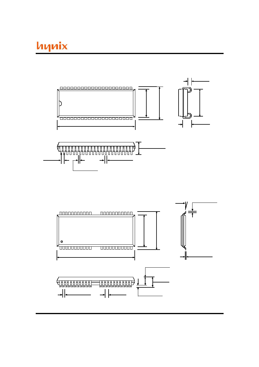
Package Dimension
42 SOJ
Unit: Inches (mm)
0.405(10.29)
MAX
0.394(10.03)
MIN
0.455(11.56)
MIN
0.471(11.96)
MAX
0.017(0.45) MAX
0.012(0.30) MIN
TYP
0.031(0.80)
0.830(21.08) MAX
0.820(20.82) MIN
0.047(1.20)
MAX
0.006(0.15) MAX
0.002(0.05) MIN
0.041(1.05) MAX
0.037(0.95) MIN
0.024(0.60) MAX
0.016(0.40) MIN
0.008(0.21) MAX
0.004(0.12) MIN
0 ~ 5
° £
1.072(27.23) MAX
0.395(10.03)
MIN
0.435(11.06)
MIN
0.445(11.30)
MAX
0.148(3.75) MAX
0.128(3.25) MIN
0.026(0.66) MIN
TYP
0.050(1.27)
0.405(10.29)
MAX
0.020(0.50) MAX
0.015(0.38) MIN
1.058(26.89) MAX
0.360(9.15)
MIN
0.380(9.65)
MAX
0.025(0.64)
MIN
0.093(2.38)
MIN
0.032(0.81) MAX
44(50) TSOP I