The GM71V(S)16160C/CL is the new
generation dynamic RAM organized 1,048,576
x 16 bit. GM71V(S)16160C/CL has realized
higher density, higher performance and various
functions by utilizing advanced CMOS process
technology. The GM71V(S)16160C/CL offers
Fast Page Mode as a high speed access mode.
M u l t i p l e x e d a d d r e s s i n p u t s p e r m i t t h e
GM71V(S)16160C/CL to be packaged in
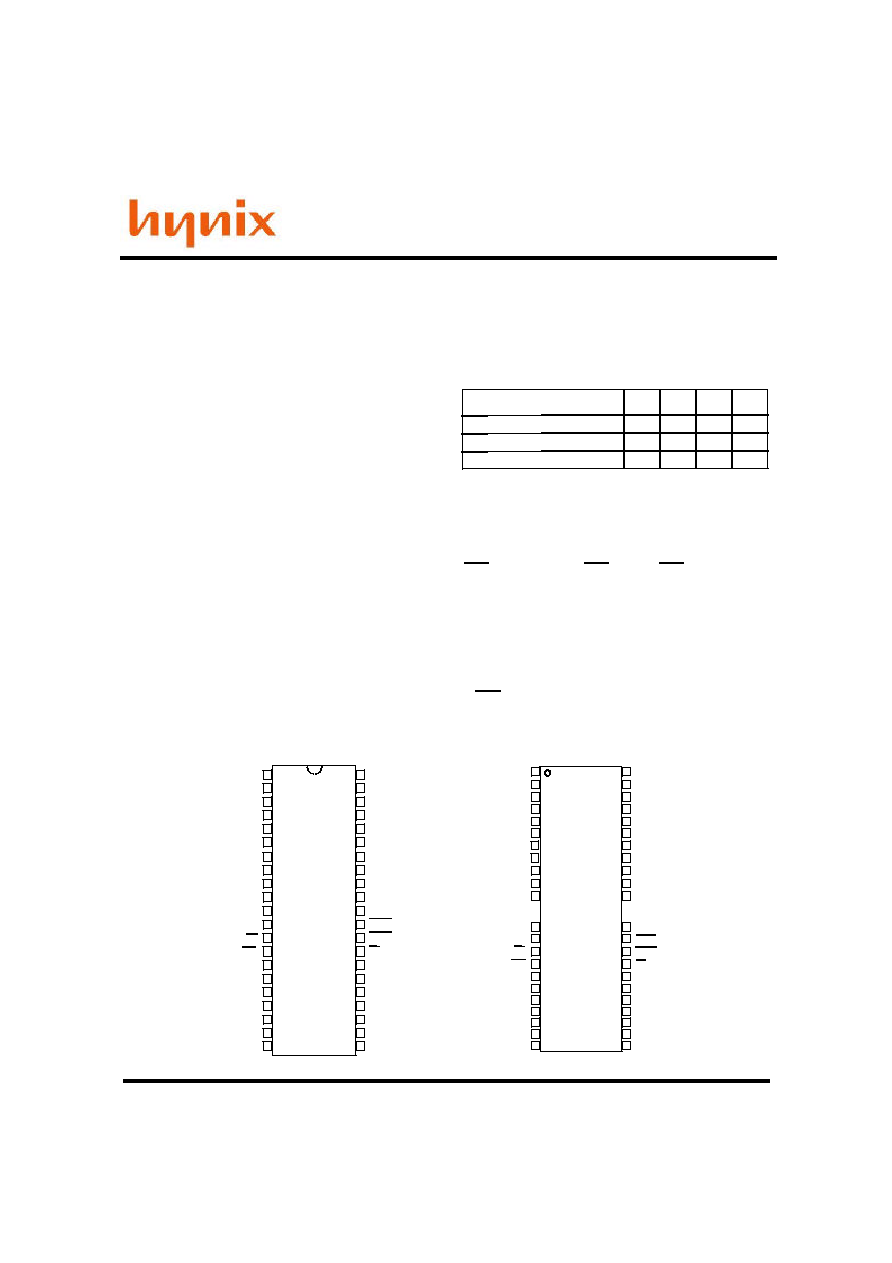
standard 400 mil 42pin plastic SOJ, and
standard 400mil 44(50)pin plastic TSOP II. The
package size provides high system bit densities
and is compatible with widely available
automated testing and insertion equipment.
Description
Features
* 1,048,576 Words x 16 Bit Organization
* Fast Page Mode Capability
* Single Power Supply (3.3V+/-0.3V)
* Fast Access Time & Cycle Time
Pin Configuration
1,048,576 WORDS x 16 BIT
CMOS DYNAMIC RAM
GM71VS16160CL
* Low Power
Active : 396/360/324mW (MAX)
Standby : 7.2mW (CMOS level : MAX)
0.54mW (L-version : MAX)
* RAS Only Refresh, CAS before RAS Refresh,
Hidden Refresh Capability
* All inputs and outputs TTL Compatible
*4096 Refresh Cycles/64ms
* 4096 Refresh Cycles/128ms (L-version)
* Self Refresh Operation (L-version)
* Battery Back Up Operation (L-version)
* 2 CAS byte Control
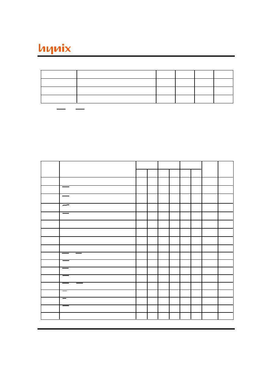
(Unit: ns)
GM71V(S)16160C/CL-5
GM71V(S)16160C/CL-6
GM71V(S)16160C/CL-7
t
RAC
t
CAC
t
RC
t
PC
50
60
13
15
90
110
35
40
70
18
130
45
(Top View)
44(50) TSOP II
42 SOJ
42
43
44
45
46
40
41
33
30
31
32
27
28
29
26
34
35
36
47
48
49
50
NC
NC
V
SS
I/O15
I/O14
I/O13
I/O12
I/O11
I/O10
I/O9
I/O8
V
SS
LCAS
UCAS
OE
A8
A7
A6
A5
A4
V
SS
A9
V
SS
I/O15
I/O14
I/O13
I/O12
38
39
40
41
42
I/O11
I/O10
I/O9
I/O8
NC
32
33
34
35
36
V
SS
37
LCAS
UCAS
OE
29
30
31
A9
A8
A7
26
27
28
A6
A5
A4
23
24
25
V
SS
22
11
1
2
3
4
5
7
8
9
10
6
15
16
17
18
19
20
21
22
23
24
25
NC
NC
I/O0
I/O1
I/O2
I/O3
I/O4
I/O5
I/O6
I/O7
V
CC
NC
WE
RAS
A11
A10
A0
A1
V
CC
V
CC
A2
A3
V
CC
I/O0
I/O1
I/O2
I/O3
1
2
3
4
5
I/O4
I/O5
I/O6
I/O7
NC
7
8
9
10
11
V
CC
6
NC
WE
RAS
12
13
14
A11
A10
A0
15
16
17
A1
A2
A3
18
19
20
V
CC
21
GM71V16160C
Rev 0.1 / Apr'01
GM71VS16160CL
GM71V16160C
Rev 0.1 / Apr'01
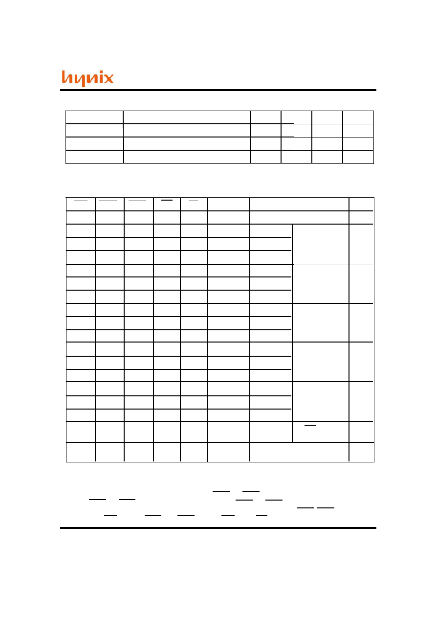
Pin Description
Pin
Function
Pin
Function
A0-A11
A0-A11
I/O0-I/O15
RAS
WE
V
CC
V
SS
NC
Address Inputs
Refresh Address Inputs
Data Input/ Data Output
Row Address Strobe
Read/Write Enable
Power (+3.3V)
Ground
No Connection
Ordering Information
UCAS, LCAS
Column Address Strobe
OE
Output Enable
Absolute Maximum Ratings*
Note: Operation at or above Absolute Maximum Ratings can adversely affect device reliability.
Type No.
Access Time
Package
GM71V(S)16160CJ/CLJ -5
GM71V(S)16160CJ/CLJ -6
GM71V(S)16160CJ/CLJ -7
50ns
60ns
70ns
400 Mil
42 Pin
Plastic SOJ
50ns
60ns
70ns
400 Mil
44(50) Pin
Plastic TSOP II
GM71V(S)16160CT/CLT -5
GM71V(S)16160CT/CLT -6
GM71V(S)16160CT/CLT -7
Symbol
Parameter
Rating
Unit
T
A
T
STG
V
IN/OUT
V
CC
I
OUT
0 ~ 70
-55 ~ 125
-0.5 ~ Vcc+0.5
(<=4.6V(MAX))
-0.5 ~ 4.6
50
Ambient Temperature under Bias
Storage Temperature
Voltage on any Pin Relative to V
SS
Supply Voltage Relative to V
SS
Short Circuit Output Current
V
V
mA
P
D
1.0
Power Dissipation
W
C
C
GM71VS16160CL
GM71V16160C
Rev 0.1 / Apr'01
Truth Table
Notes: 1. H: High (inactive) L: Low(active) D: H or L
2.
t
WCS
>= 0ns Early write cycle
t
WCS
<= 0ns Delayed write cycle
3. Mode is determined by the OR function of the UCAS and LCAS. (Mode is set by earliest of
UCAS and LCAS active edge and reset by the latest of UCAS and LCAS inactive edge.) However
write OPERATION and output High-Z control are done independently by each UCAS,LCAS.
ex) if RAS = H to L, UCAS = H, LCAS = L, then CAS-before-RAS refresh cycle is selected.
RAS
LCAS UCAS
WE
OE
H
L
L
L
D
H
L
H
D
H
H
L
D
H
H
H
D
D
L
L
Output
Open
Valid
Valid
Valid
Lower byte
Upper byte
Word
Operation
Standby
RAS-only
Refresh cycle
Read cycle
L
L
L
L
L
L
H
L
H
Early write cycle
L
H
L
L
H
Open
Open
Open
L
L
L
L
Undefined
Delayed Write
cycle
L
L
L
H
H
H to L
L
CBR Refresh
or
Self Refresh
(L-series)
H to L
H
L
H to L
L
L
Notes
1,3
1,3
1,3
1,3
1,3
1,2,3
1,2,3
1,3
Lower byte
Upper byte
Word
Lower byte
Upper byte
Word
Lower byte
Upper byte
Word
Undefined
Undefined
Open
Open
Open
Open
Open
Valid
Valid
Valid
Word
Word
Word
Word
Read-modify
-write cycle
Read cycle
(Output disabled)
D
D
H to L
H to L
H to L
L
L
L
L
L
L
L
H
L
L
L
L
H
D
D
L
H
H
H
H
L
D
D
D
D
D
D
L to H
L to H
L to H
L
L
L
L
Recommended DC Operating Conditions (T
A
= 0 ~
+
70C)
Symbol
Parameter
Unit
V
CC
V
IH
V
IL
Supply Voltage
Input High Voltage
Input Low Voltage
V
V
V
Max
3.6
V
CC
+ 0.3
0.8
Typ
3.3
-
-
Min
3.0
2.0
-0.3
Note: All voltage referred to Vss.
The supply voltage with all VCC pins must be on the same level. The supply voltage with all VSS pins must be
on the same level.
GM71VS16160CL
GM71V16160C
Rev 0.1 / Apr'01
DC Electrical Characteristics (V
CC
= 3.3V+/-0.3V, Vss = 0V, T
A
= 0 ~ 70C)
Symbol
Parameter
Note
V
OH
V
OL
Output Level
Output "H" Level Voltage (I
OUT
=
-2mA
)
Unit
V
V
Max
V
CC
0.4
Min
2.4
0
Output Level
Output "L" Level Voltage (I
OUT
=
2mA)
I
CC1
Operating Current
Average Power Supply Operating Current
(RAS, UCAS or LCAS Cycling
:
t
RC
=
t
RC
min)
I
CC2
mA
Standby Current (TTL)
Power Supply Standby Current
(RAS, UCAS, LCAS = V
IH
,
D
OUT
=
High-Z)
2
-
I
CC3
RAS Only Refresh Current
Average Power Supply Current
RAS Only Refresh Mode
(t
RC
=
t
RC
min)
I
CC4
I
CC5
mA
Standby Current (CMOS)
Power Supply Standby Current
(RAS, UCAS or LCAS >= V
CC
- 0.2V, D
OUT
= High-Z)
1
-
I
CC6
CAS-before-RAS Refresh Current
(t
RC
=
t
RC
min)
150
-
I
L(I)
uA
10
-10
I
L(O)
uA
10
-10
Input Leakage Current
Any Input (0V
<=
V
IN
<=
4.6V)
Output Leakage Current
(D
OUT
is Disabled, 0V
<=
V
OUT
<= 4.
6V)
Fast Page Mode Current
Average Power Supply Current
Fast Page Mode
(t
PC
= t
PC
min)
uA
mA
110
-
50ns
60ns
70ns
100
90
-
1, 2
-
mA
2
mA
1, 3
-
110
-
50ns
60ns
70ns
100
90
-
-
115
-
50ns
60ns
70ns
105
95
-
mA
110
-
50ns
60ns
70ns
-
-
100
90
I
CC7
I
CC8
Battery Back Up Operating Current
(Standby with CBR Refresh)
(t
RC
=31.3us
,
t
RAS
<=
0.3
us,
D
OUT
=
High-Z)
400
-
4,5
uA
I
CC9
uA
Self-Refresh Mode Current
(RAS, UCAS or LCAS<=0.2V
,
D
OUT
=
High-Z)
250
-
5
Note: 1. I
CC
depends on output load condition when the device is selected.
I
CC
(max) is specified at the output open condition.
2. Address can be changed once or less while RAS = V
IL
.
3. Address can be changed once or less while
U
CAS and LCAS = V
IH
.
4. UCAS = L (<=0.2) and LCAS = L (<=0.2) while RAS = L (<=0.2).
5. L-version.
mA
5
-
1
Standby Current RAS = V
IH
U
CAS, LCAS = V
IL
D
OUT
=
Enable
5
GM71VS16160CL
GM71V16160C
Rev 0.1 / Apr'01
Read, Write, Read-Modify-Write and Refresh Cycles (Common Parameters)
Capacitance (V
CC
= 3.3V+/-0.3V, T
A
= 25C)
Symbol
Parameter
Note
C
I1
C
I2
C
I/O
Input Capacitance (Address)
Input Capacitance (Clocks)
Output Capacitance (Data-In/Out)
1
1
1, 2
Unit
pF
pF
pF
Max
5
7
7
Min
-
-
-
Note: 1. Capacitance measured with Boonton Meter or effective capacitance measuring method.
2. UCAS and LCAS = V
IH
to disable D
OUT
.
AC Characteristics (V
CC
= 3.3V+/-0.3V, T
A
= 0 ~
+
70C, Note 1, 2, 18, 19, 20)
Test Conditions
Input rise and fall times : 5 ns
Output timing reference levels : 0.8V, 2.0V
Input timing reference levels : 0.8V, 2.0V
Output load : 1TTL gate + C
L
(100 pF)
(Including scope and jig)
Symbol
Parameter
Note
Max
Unit
Min
Max
Min
Max
Min
t
RC
Random Read or Write Cycle Time
90
-
110
-
130
-
t
RP
RAS Precharge Time
30
-
40
-
50
-
t
RAS
RAS Pulse Width
50
10,000
60
10,000
70
10,000
t
CAS
CAS Pulse Width
10,000
10,000
10,000
15
18
t
ASR
Row Address Set up Time
0
-
-
-
0
0
t
RAH
Row Address Hold Time
8
-
-
-
10
10
t
ASC
Column Address Set-up Time
0
-
-
-
0
0
t
CAH
Column Address Hold Time
-
-
-
10
15
t
RCD
RAS to CAS Delay Time
18
45
45
52
20
20
3
t
RAD
RAS to Column Address Delay Time
13
30
30
35
15
15
4
t
RSH
RAS Hold Time
13
-
-
-
15
18
t
CSH
CAS Hold Time
50
-
-
-
60
70
t
CRP
CAS to RAS Precharge Time
5
-
-
-
5
5
t
T
Transition Time (Rise and Fall)
3
50
50
50
3
3
7
t
DZO
OE Delay Time from D
IN
0
-
-
-
0
0
t
DZC
CAS Delay Time from D
IN
0
-
-
-
0
0
GM71V(S)16160
C/CL-5
OE to D
IN
Delay Time
13
-
-
-
15
18
5
6
6
t
CP
CAS Precharge Time
8
-
10
-
10
-
t
ODD
GM71V(S)16160
C/CL-6
GM71V(S)16160
C/CL-7
ns
ns
ns
ns
ns
ns
ns
ns
ns
ns
ns
ns
ns
ns
ns
ns
ns
ns
13
8
24
21
21
22
23