GM71VS64803CL
8,388,608 WORDS x 8 BIT
CMOS DYNAMIC RAM
Description
Features
*8,388,608 Words x 8 Bit
* Extended Data Out (EDO) Mode Capability
* Fast Access Time & Cycle Time
Power dissipation
- Active : 450mW/414mW(MAX)
- Standby : 1.8 mW ( CMOS level : MAX )
0.54mW ( L-Version : MAX)
*EDO page mode capability
*Access time : 50ns/60ns (max)
*Refresh cycles
- RAS only Refresh
8192 cycles/64 ms (GM71V64803C)
8192 cycles/128ms (GM71VS64803CL)(L_Version)
*CBR & Hidden Refresh
4096 cycles/64 ms (GM71V64803C)
4096 cycles/128 ms (GM71VS64803CL)( L-Version )
*4 variations of refresh
-RAS-only refresh
-CAS-before-RAS refresh
-Hidden refresh
-Self refresh (L-Version)
*Single Power Supply of 3.3V+/-10 % with a built-in VBB generator
*Battery Back Up Operation ( L-Version )
(Unit: ns)
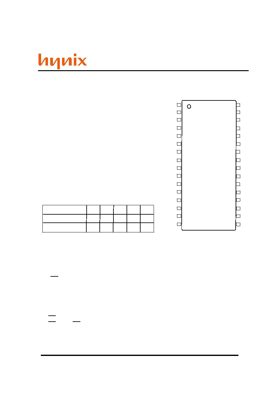
Pin Configuration
The GM71V(S)64803C/CL is the new generation
dynamic RAM organized 8,388,608 words by 8bits.
The GM71V(S)64803C/CL utilizes advanced CMOS
Silicon Gate Process Technology as well as
advanced circuit techniques for wide operating
margins, both internally and to the system user.
System oriented features include single power supply
of 3.3V+/-10% tolerance, direct interfacing
capability with high performance logic families such
as Schottky TTL.
The GM71V(S)64803C/CL offers Extended Data
Out(EDO) Mode as a high speed access mode.
GM71V(S)64803C/CL-5
GM71V(S)64803C/CL-6
t
RAC
t
AA
t
RC
t
HPC
50
60
25
30
84
104
20
25
13
15
t
CAC
32 SOJ / TSOP II
IO2
(Top View)
1
2
3
4
5
6
7
8
9
10
11
12
13
14
15
16
VCC
IO0
IO1
IO3
NC
VCC
/WE
/RAS
A0
A1
A2
A3
A4
A5
VCC
32
17
18
19
20
21
22
23
24
25
26
27
28
29
30
31
VSS
A6
A7
A8
A9
A10
A11
A12
/OE
/CAS
VSS
IO6
IO7
VSS
IO4
IO5
GM71V64803C
Rev 0.1 / Apr'01
Pin Description
Pin
Function
Pin
Function
A0-A12
A0-A12
RAS
CAS
WE
V
CC
V
SS
NC
Address Inputs
Refresh Address Inputs
Row Address Strobe
Column Address Strobe
Write Enable
Power (+3.3V)
Ground
No Connection
Absolute Maximum Ratings*
Symbol
Parameter
Rating
Unit
T
STG
V
T
V
CC
I
OUT
-55 to 125
-0.5 to V
CC
+ 0.5
(MAX ; 4.6V)
-0.5 to 4.6
50
Storage Temperature (Plastic)
Voltage on any Pin Relative to V
SS
Voltage on V
CC
Relative to V
SS
Short Circuit Output Current
C
V
V
mA
P
T
1.0
Power Dissipation
W
*Note : Operation at or above Absolute Maximum Ratings can adversely affect device reliability.
Recommended DC Operating Conditions (T
A
= 0 ~ 70C)
Symbol
Parameter
Unit
V
CC
V
IH
V
IL
Supply Voltage
Input High Voltage
Input Low Voltage
V
V
V
Max
3.6
Vcc+0.3
0.8
Typ
3.3
-
-
Min
3.0
2.0
-0.3
OE
Output Enable
I/O0 - I/O7
Data Input / Output
Ordering Information
Type No.
Access Time
Package
GM71V(S)64803C/CLJ-5
GM71V(S)64803C/CLJ-6
50ns
60ns
400 Mil
32Pin
Plastic SOJ
GM71V(S)64803C/CLT-5
GM71V(S)64803C/CLT-6
50ns
60ns
400 Mil
32Pin
Plastic TSOP II
Notes
1,2
1
1
V
SS
Supply Voltage
V
0
0
0
2
T
A
70
Ambient Temperature under Bias
C
-
0
GM71VS64803CL
GM71V64803C
Rev 0.1 / Apr'01
DC Electrical Characteristics: (V
CC
= 3.3V+/-10%, T
A
= 0 ~ 70C)
Symbol
Parameter
Note
V
OH
V
OL
Output Level
Output Level Voltage (I
OUT
= -2mA)
Unit
V
V
Max
V
CC
0.4
Min
2.4
0
Output Level
Output Level Voltage (I
OUT
= 2mA)
I
CC1
125
-
Operating Current (
t
RC
=
t
RC
min)
50ns
mA
60ns
115
-
I
CC2
mA
Standby Current (TTL interface)
Power Supply Standby Current
(RAS, CAS= V
IH
, D
OUT
= High-Z)
2
-
I
CC3
mA
RAS-Only Refresh Current
( t
RC
= t
RC
min)
I
CC4
mA
Extended Data Out page Mode Current
(RAS = V
IL
, CAS, Address Cycling: t
HPC
= t
HPC
min)
-
50ns
60ns
-
110
-
50ns
60ns
100
-
I
CC6
mA
CAS-before-RAS Refresh Current
(t
RC
= t
RC
min)
-
50ns
60ns
-
I
CC8
mA
Standby Current (CMOS)
Power Supply Standby Current
RAS = V
IH
, CAS = V
IL
,
D
OUT
= Enable
5
-
I
I(L)
5
-5
I
O(L)
5
-5
Input Leakage Current, Any Input
(0V<=V
IN
<=Vcc)
Output Leakage Current
(D
OUT
is Disabled, 0V<=V
OUT
<=Vcc)
Note: 1. I
CC
depends on output load condition when the device is selected. I
CC(max)
is specified at the
output open condition.
2. Address can be changed once or less while RAS = V
IL
.
3. Measured with one sequential address change per EDO cycle, t
HPC
.
4. V
IH
>=V
CC
-0.2V, 0V<=V
IL
<=0.2V
5. L-Version
125
115
145
135
500
400
Battery Back Up Operating Current(Standby with CBR)
(tRC=31.25us,tRAS=300ns,Dout=High-Z)
Self Refresh Current
(RAS, CAS <=0.2V,Dout=High-Z)
I
CC7
I
CC9
Standby Current(L_Version)
uA
300
-
uA
mA
CMOS interface
(RAS, CAS>=V
CC
-0.2V, D
OUT
= High-Z)
0.5
-
-
-
I
CC5
1,2
2
1
1,3
4, 5
uA
uA
uA
4
5
GM71VS64803CL
GM71V64803C
Rev 0.1 / Apr'01
Symbol
Parameter
Note
C
I1
C
I2
C
I/O
Input Capacitance (Address)
Input Capacitance (Clocks)
Output Capacitance (Data-in,Data-Out)
1
1
1, 2
Unit
pF
pF
pF
Max
5
7
7
Typ
-
-
-
Note: 1. Capacitance measured with Boonton Meter or effective capacitance measuring method.
2. RAS, CAS = V
IH
to disable D
OUT
.
Capacitance (V
CC
= 3.3V+/-10%, T
A
= 25C)
Read, Write, Read-Modify-Write and Refresh Cycles (Common Parameters)
AC Characteristics (V
CC
= 3.3V+/-10%, T
A
= 0 ~ 70C, Notes 1, 2,19)
Test Conditions
Input rise and fall times : 2ns Output timing reference levels : V
OL
/V
OH
= 0.8/2.0V
Input level : V
IL
/V
IH
= 0.0/3.0V Output load : 1 TTL gate+C
L
(100pF)
Input timing reference levels : V
IL
/V
IH
= 0.8/2.0V (Including scope and jig)
Symbol
Parameter
Min
GM71V(S)64803C/CL-5
Max
t
RC
Random Read or Write Cycle Time
t
RP
RAS Precharge Time
t
RAS
RAS Pulse Width
t
CAS
CAS Pulse Width
t
ASR
Row Address Set-up Time
t
RAH
Row Address Hold Time
t
ASC
Column Address Set-up Time
t
CAH
Column Address Hold Time
t
RCD
RAS to CAS Delay Time
4
t
RAD
RAS to Column Address Delay Time
3
t
RSH
RAS Hold Time
t
CSH
CAS Hold Time
t
CRP
CAS to RAS Precharge Time
Max
Min
84
104
40
60
10
0
10
0
10
14
12
15
40
5
30
50
8
0
8
0
8
12
10
13
35
5
-
-
-
25
37
-
-
-
-
10000
-
-
-
-
10000
-
-
-
-
45
30
-
-
-
Unit
Notes
ns
ns
ns
ns
ns
ns
ns
ns
ns
ns
ns
ns
ns
t
T
TransitionTime (Rise and Fall)
2
2
50
50
ns
t
ODD
OE to D
IN
Delay Time
t
DZO
OE Delay Time from D
IN
t
DZC
CAS Delay Time from D
IN
15
0
0
13
0
0
-
-
-
-
-
-
ns
ns
ns
GM71V(S)64803C/CL-6
t
CP
CAS Precharge Time
10
8
-
-
ns
10000
10000
5
6
6
7
t
REF
Refresh Period
-
-
64
64
ms
Refresh Period ( L-Version )
-
-
128
128
ms
8192
cycles
8192
cycles
GM71VS64803CL
GM71V64803C
Rev 0.1 / Apr'01
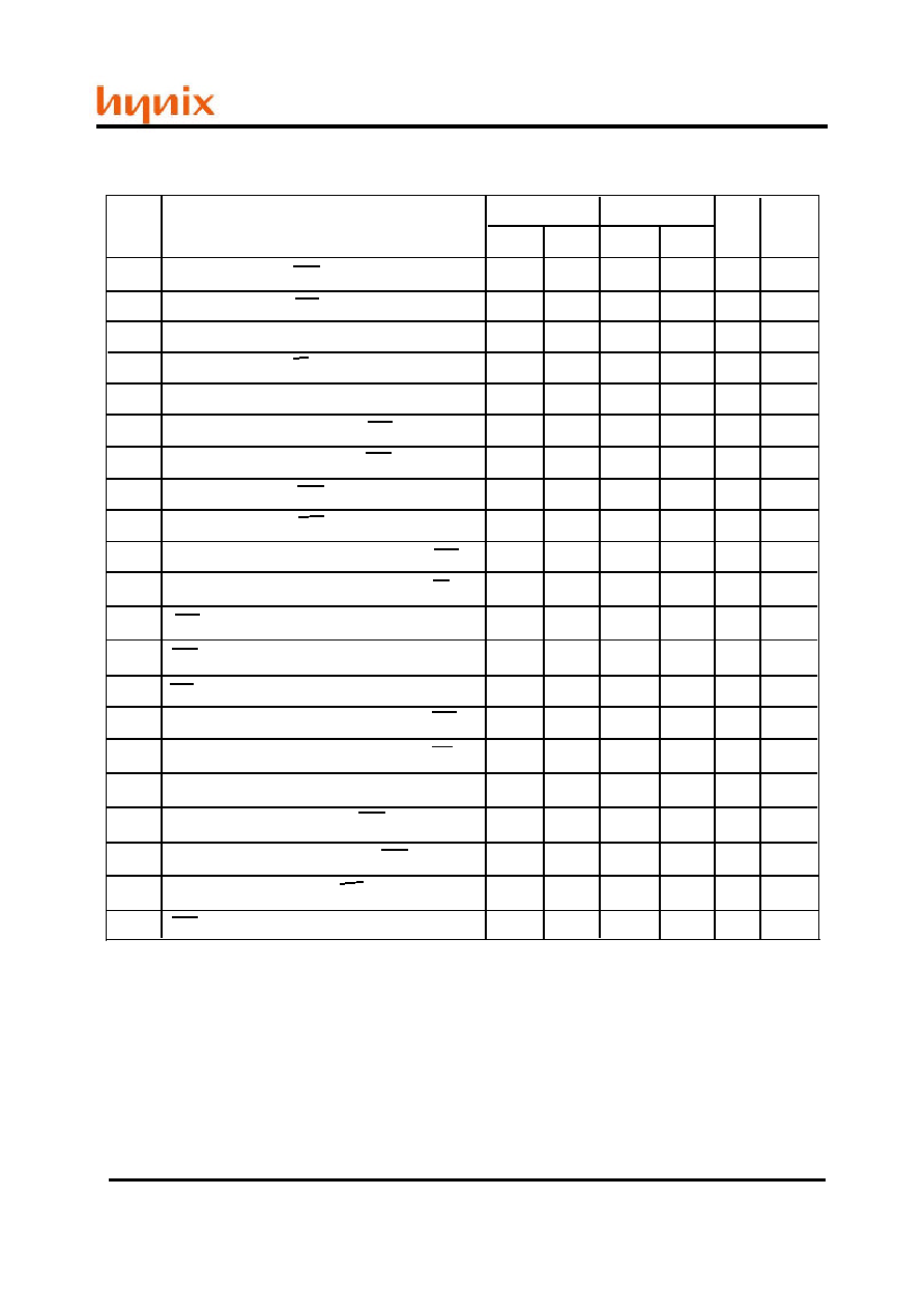
Read Cycles
Symbol
Parameter
Min
GM71V(S)64803C/CL-5 GM71V(S)64803C/CL-6
Max
Max
Min
-
-
-
-
0
0
0
30
-
-
0
0
0
25
-
-
-
25
13
50
60
15
30
-
-
-
Unit
Notes
ns
ns
ns
ns
ns
ns
ns
ns
-
-
t
RAC
t
CAC
t
AA
t
RCS
t
RCH
t
RRH
t
RAL
t
CAL
Access Time from RAS
Access Time from CAS
Access Time from Column Address
Read Command Set-up Time
Read Command Hold Time to CAS
Read Command Hold Time to RAS
Column Address to RAS Lead Time
Column Address to CAS Lead Time
8,9
t
OAC
Access Time from OE
-
13
-
15
ns
15
-
18
-
9,10,17
9,11,17
ns
ns
t
RDD
t
WDD
RAS to D
IN
Delay Time
ns
t
OFR
Output Buffer Turn-off Delay Time from RAS
ns
t
WEZ
Output Buffer Turn-off Delay Time from WE
13
13
-
-
13
-
15
13
-
15
-
15
-
-
15
-
13
ns
ns
ns
t
CLZ
t
OH
t
CDD
CAS to Output in Low - Z
Output Data Hold Time
CAS to D
IN
Delay Time
-
15
-
ns
ns
t
OHR
t
OEZ
Output Data Hold Time from RAS
Output Buffer Turn-off Delay Time from OE
ns
t
OFF
0
3
-
-
13
15
13
-
15
-
-
-
3
-
-
-
-
WE to D
IN
Delay Time
13,21
13
ns
t
RCHR
Read Command Hold Time from RAS
50
-
60
-
ns
t
OHO
Output data hold time from OE
3
-
3
-
0
Output Buffer Turn-off Delay Time from CAS
12
9
12
13,21
13
3
3
21
5
21
GM71VS64803CL
GM71V64803C
Rev 0.1 / Apr'01