
G M 7 2 V 6 6 4 4 1 E T / E L T
4 , 1 9 4 , 3 0 4 W O R D x 4 B I T x 4 B A N K
S Y N C H R O N O U S D Y N A M I C R A M
Description
T h e G M 7 2 V 6 6 4 4 1 E T / E L T i s a s y n c h r o n o u s
d y n a m i c r a n d o m a c c e s s m e m o r y c o m p r i s e d o f
6 7 , 1 0 8 , 8 6 4 m e m o r y c e l l s a n d l o g i c i n c l u d i n g
i n p u t a n d o u t p u t c i r c u i t s o p e r a t i n g s y n c h r o n o u s l y
b y r e f e r r i n g t o t h e p o s i t i v e e d g e o f t h e e x t e r n a l l y
p r o v i d e d C l o c k .
T h e G M 7 2 V 6 6 4 4 1 E T / E L T p r o v i d e s f o u r b a n k s
o f 4 , 1 9 4 , 3 0 4 w o r d b y 4 b i t t o r e a l i z e h i g h
b a n d w i d t h w i t h t h e C l o c k f r e q u e n c y u p t o 1 4 3
M h z .
F e a t u r e s
* P C 1 3 3 / P C 1 0 0 / P C 6 6 C o m p a t i b l e
- 7 ( 1 4 3 M H z ) / - 7 5 ( 1 3 3 M H z ) / - 8 ( 1 2 5 M H z )
- 7 K ( P C 1 0 0 , 2 - 2 - 2 ) / - 7 J ( P C 1 0 0 , 3 - 2 - 2 )
* 3 . 3 V s i n g l e P o w e r s u p p l y
* L V T T L i n t e r f a c e
* M a x C l o c k f r e q u e n c y
1 4 3 / 1 3 3 / 1 2 5 / 1 0 0 M H z
* 4 , 0 9 6 r e f r e s h c y c l e p e r 6 4 m s
* T w o k i n d s o f r e f r e s h o p e r a t i o n
A u t o r e f r e s h / S e l f r e f r e s h
* P r o g r a m m a b l e b u r s t a c c e s s c a p a b i l i t y ;
- S e q u e n c e : S e q u e n t i a l / I n t e r l e a v e
- L e n g t h : 1 / 2 / 4 / 8 / F P
* P r o g r a m m a b l e C A S l a t e n c y : 2 / 3
* 4 B a n k s c a n o p e r a t e i n d e p e n d e n t l y o r
s i m u l t a n e o u s l y
* B u r s t r e a d / b u r s t w r i t e o r b u r s t r e a d / s i n g l e
w r i t e o p e r a t i o n c a p a b i l i t y
* I n p u t a n d o u t p u t m a s k i n g b y D Q M i n p u t
* O n e C l o c k o f b a c k t o b a c k r e a d o r w r i t e
c o m m a n d i n t e r v a l
* S y n c h r o n o u s P o w e r d o w n a n d C l o c k
s u s p e n d c a p a b i l i t y w i t h o n e C l o c k l a t e n c y
f o r b o t h e n t r y a n d e x i t
* J E D E C S t a n d a r d 5 4 P i n 4 0 0 m i l T S O P I I P a c k a g e
Pin Configuration
P i n N a m e
C L K
C K E
C S
R A S
C A S
W E
A 0 ~ A 9 , A 1 1
A 1 0 / A P
B A 0 / A 1 3
~ B A 1 / A 1 2
D Q 0 ~ D Q 7
D Q M
V C C Q
V S S Q
V C C
V S S
N C
C l o c k
C l o c k E n a b l e
C h i p S e l e c t
R o w A d d r e s s S t r o b e
C o l u m n A d d r e s s S t r o b e
W r i t e E n a b l e
A d d r e s s i n p u t
A d d r e s s i n p u t o r A u t o P r e c h a r g e
B a n k s e l e c t
D a t a i n p u t / D a t a o u t p u t
D a t a i n p u t / o u t p u t M a s k
V
C C
f o r D Q
V
S S
f o r D Q
P o w e r f o r i n t e r n a l c i r c u i t
G r o u n d f o r i n t e r n a l c i r c u i t
N o C o n n e c t i o n
1
2
3
4
5
6
7
8
9
10
11
12
13
14
15
16
17
18
19
20
21
22
23
24
25
26
27
JEDEC STANDARD
400 mil 54 PIN TSOP II
(TOP VIEW)
54
53
52
51
50
49
48
47
46
45
44
43
42
41
40
39
38
37
36
35
34
33
32
31
30
29
28
V C C
N C
V C C Q
N C
D Q 0
V S S Q
N C
N C
V C C Q
N C
D Q 1
V S S Q
N C
V C C
N C
/W E
/C A S
/R A S
/C S
B A 0 / A 1 3
B A 1 / A 1 2
A 1 0 , A P
A 0
A 1
A 2
A 3
V C C
V S S
N C
V S S Q
N C
D Q 3
V C C Q
N C
N C
V S S Q
N C
D Q 2
V C C Q
N C
V S S
N C
D Q M
C L K
C K E
N C
A 1 1
A 9
A 8
A 7
A 6
A 5
A 4
V S S
-1-
T h i s d o c u m e n t i s a g e n e r a l p r o d u c t d e s c r i p t i o n a n d i s s u b j e c t t o c h a n g e w i t h o u t n o t i c e . H y n i x s e m i c o n d u c t o r d o e s n o t a s s u m e a n y
r e s p o n s i b i l i t y f o r u s e o f c i r c u i t s d e s c r i b e d . N o p a t e n t l i c e n s e s a r e i m p l i e d .
R e v . 1 . 1 / A p r . 0 1
G M 7 2 V 6 6 4 4 1 E T / E L T
R e v . 1 . 1 / A p r . 0 1
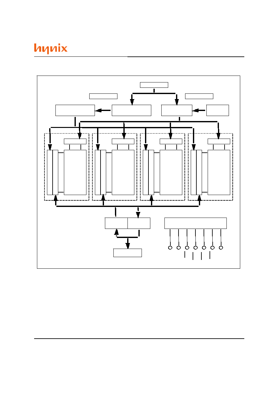
Block Diagram
A 0 t o A 1 3
A 0 t o A 9
A 0 t o A 1 3
C o l u m n a d d r e s s
c o u n t e r
C o l u m n a d d r e s s
b u f f e r
R o w a d d r e s s
c o u n t e r
R e f r e s h
c o u n t e r
I n p u t
buffer
O u t p u t
buffer
D Q 0 t o D Q 3
C o n t r o l l o g i c &
t i m i n g g e n e r a t o r
CLK
CKE
DQM
RAS
CAS
R o w d e c o d e r
M e m o r y a r r a y
B a n k 0
4 0 9 6 r o w
x 1 0 2 4 c o l u m n
x 4 b i t
Column decoder
Sense amplifier & I/O bus
R o w d e c o d e r
M e m o r y a r r a y
B a n k 1
4 0 9 6 r o w
x 1 0 2 4 c o l u m n
x 4 b i t
Column decoder
Sense amplifier & I/O bus
R o w d e c o d e r
M e m o r y a r r a y
B a n k 2
4 0 9 6 r o w
x 1 0 2 4 c o l u m n
x 4 b i t
Column decoder
Sense amplifier & I/O bus
R o w d e c o d e r
M e m o r y a r r a y
B a n k 3
4 0 9 6 r o w
x 1 0 2 4 c o l u m n
x 4 b i t
Column decoder
Sense amplifier & I/O bus
CS
WE
-2-
G M 7 2 V 6 6 4 4 1 E T / E L T
R e v . 1 . 1 / A p r . 0 1
Absolute Maximum Ratings
N o t e s : 1 . R e s p e c t t o V
S S
S y m b o l
Value
U n i t
N o t e
Parameter
V
T
- 0 . 5 to V c c + 0 . 5
(
<=
4.6 (max))
V
1
Voltage on any pin relative to V
SS
V
CC
-0.5 to +4.6
V
1
Supply voltage relative to V
SS
I
OUT
50
mA
Short circuit output current
P
T
1.0
W
Power dissipation
Topr
0 to +70
C
Operating temperature
Tstg
-55 to +125
C
Storage temperature
Notes : 1. All voltage referred to V
SS
.
2. V
IH
(max) = 5.6V for pulse width <= 3ns
3. V
IL
(min) = -2.0V for pulse width <= 3ns
Recommended DC Operating Conditions (Ta = 0 to + 70C)
Symbol
Min
Unit
Note
V
CC
, V
CCQ
V
1
V
SS
, V
SSQ
V
Input high voltage
V
IH
V
1, 2
Input low voltage
V
IL
V
1,3
Supply voltage
Parameter
Max
3.0
3.6
0
0
2.0
Vcc+0.3
-0.3
0.8
-3-
GM72V66441ET/ELT
Rev. 1.1/Apr.01
DC Characteristics (Ta = 0 to 70C, V
CC
, V
CCQ
= 3.3 V +/- 0.3 V, V
SS
, V
SSQ
= 0 V)
Parameter
Symbol
Unit Test conditions Notes
Operating
current
Standby current in
power down
I
CC2P
Self refresh current
I
CC6
mA
V
IH
>=V
CC
- 0.2
V
IL
<=0.2V
7
Burst length= 1
t
RC
= min
1, 2, 3
CKE = V
IL
,
t
CK
= 12 ns
5
I
CC1
mA
mA
Standby current in
power down
(input signal stable)
I
CC2PS
CKE=V
IL
,
t
CK
= infinity
6
mA
Standby current in
non power down
(CAS Latency=2)
I
CC2N
CKE,CS = V
IH
,
t
CK
= 12ns
4
mA
Standby current in
non power down
(input signal stable)
I
CC2NS
CKE = V
IH
,
t
CK
= infinity
4
mA
Active standby current
in power down
I
CC3P
CKE = V
IL
,
t
CK
= 12 ns,
DQ = High-Z
1,2,5
mA
Active standby current
in power down
(input signal stable)
I
CC3PS
CKE = V
IL
,
t
CK
= infinity
2,6
mA
Active standby current
in non power down
I
CC3N
CKE,CS = V
IH
,
t
CK
= 12 ns,
DQ = High-Z
1,2,4
mA
Active standby current
in non power down
(input signal stable)
I
CC3NS
CKE = V
IH
,
t
CK
= infinity
2,9
mA
Burst
operating
current
I
CC4
t
CK
= min
BL = 4
1,2,3
mA
( CL= 2 )
I
CC4
mA
( CL= 3 )
Refresh current
t
RC
= min
3
I
CC5
mA
7,8
6,8
- 8
Max
80
150
Max
-7J
80
120
- 75
Max
85
150
Max
-7K
80
120
- 7
Max
1
85
2
2
15
12
6
5
20
120
150
160
0.4
0.4
30
-4-

GM72V66441ET/ELT
Rev. 1.1/Apr.01
Notes : 1. I
CC
depends on output load condition when the device is selected. I
CC (
max) is specified at the
output open condition.
2. One bank operation.
3. Addresses are changed once per one cycle.
4. Addresses are changed once per two cycles.
5. After Power down mode, CLK operating current.
6. After Power down mode, no CLK operating current.
7. After self refresh mode set, self refresh current.
8. L-Version.
9. Input signals are V
I H
or V
IL
fixed.
Capacitance (Ta = 25C, V
CC
, V
CCQ
= 3.3 V +/-0.3 V)
Input leakage current
I
LI
uA
0 <=Vin <=V
CC
Output leakage current
I
LO
uA
0<=Vout<=V
CC
DQ = disable
Output high voltage
V
OH
V
I
OH
= -2 mA
Output low voltage
V
OL
V
I
OL
=2 mA
-1
1
-1.5
1.5
-
0.4
Parameter
Symbol
Unit Test conditions Notes
Min
Max
- 7, -75, - 8, - 7K, - 7J
2.4
-
Notes : 1. Capacitance measured with Boonton Meter or effective capacitance measuring method.
2. DQM = V
I H
to disable Dout.
3. This parameter is sampled and not 100% tested.
4. Measured with 1.4 V bias and 200mV swing at the pin under measurement.
Parameter
Input capacitance (CLK)
Input capacitance (Signals)
Output capacitance (DQ)
Symbol
C
I1
C
I2
C
O
Min.
2.5
2.5
4.0
Max.
4
5
6.5
Unit
pF
pF
pF
Notes
1, 3, 4
1, 3, 4
1, 2, 3, 4
DC Characteristics (Ta = 0 to 70C, V
CC
, V
CCQ
= 3.3 V +/- 0.3 V, V
SS
, V
SSQ
= 0 V)
(Continued)
-5-