GM72V66841ET/ELT
2,097,152 WORD x 8 BIT x 4 BANK
SYNCHRONOUS DYNAMIC RAM
Description
The GM72V66841ET/ELT is a synchronous
dynamic random access memory comprised of
67,108,864 memory cells and logic including
input and output circuits operating synchronously
by referring to the positive edge of the externally
provided Clock.
The GM72V66841ET/ELT provides four banks
of 2,097,152 word by 8 bit to realize high
bandwidth with the Clock frequency up to 143
Mhz.
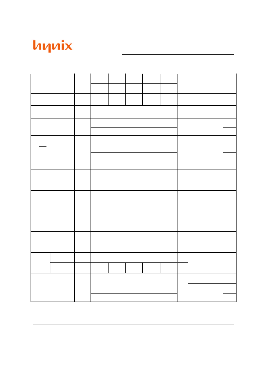
Pin Configuration
Pin Name
CLK
CKE
CS
RAS
CAS
WE
A0~A9,A11
A10 / AP
BA0/A13
~BA1/A12
DQ0~DQ7
DQM
VCCQ
VSSQ
VCC
VSS
NC
Clock
Clock Enable
Chip Select
Row Address Strobe
Column Address Strobe
Write Enable
Address input
Address input or Auto Precharge
Bank select
Data input / Data output
Data input / output Mask
V
CC
for DQ
V
SS
for DQ
Power for internal circuit
Ground for internal circuit
No Connection
1
2
3
4
5
6
7
8
9
10
11
12
13
14
15
16
17
18
19
20
21
22
23
24
25
26
27
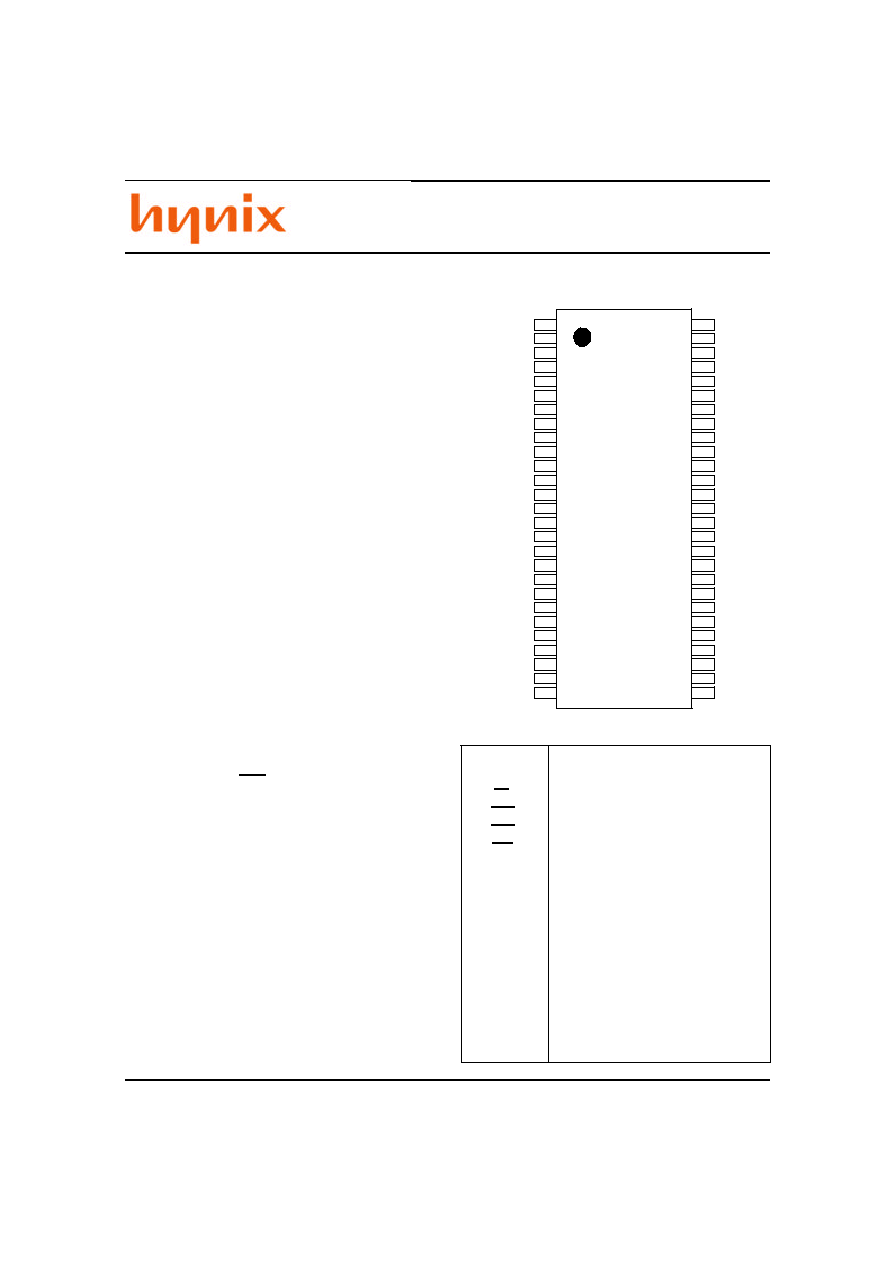
JEDEC STANDARD
400 mil 54 PIN TSOP II
(TOP VIEW)
54
53
52
51
50
49
48
47
46
45
44
43
42
41
40
39
38
37
36
35
34
33
32
31
30
29
28
VCC
DQ0
VCCQ
NC
DQ1
VSSQ
NC
DQ2
VCCQ
NC
DQ3
VSSQ
NC
VCC
NC
/WE
/CAS
/RAS
/CS
BA0/A13
BA1/A12
A10,AP
A0
A1
A2
A3
VCC
VSS
DQ7
VSSQ
NC
DQ6
VCCQ
NC
DQ5
VSSQ
NC
DQ4
VCCQ
NC
VSS
NC
DQM
CLK
CKE
NC
A11
A9
A8
A7
A6
A5
A4
VSS
Features
* PC133/PC100/PC66 Compatible
-7(143MHz)/-75(133MHz)/-8(125MHz)
-7K(PC100,2-2-2)/-7J(PC100,3-2-2)
* 3.3V single Power supply
* LVTTL interface
* Max Clock frequency
143/133/125/100MHz
* 4,096 refresh cycle per 64 ms
* Two kinds of refresh operation
Auto refresh / Self refresh
* Programmable burst access capability ;
- Sequence:Sequential / Interleave
- Length :1/2/4/8/FP
* Programmable CAS latency : 2/3
* 4 Banks can operate independently or
simultaneously
* Burst read/burst write or burst read/single
write operation capability
* Input and output masking by DQM input
* One Clock of back to back read or write
command interval
* Synchronous Power down and Clock
suspend capability with one Clock latency
for both entry and exit
* JEDEC Standard 54Pin 400mil TSOP II
Package
-1-
This document is a general product description and is subject to change without notice. Hynix semiconductor does not assume any
responsibility for use of circuits described. No patent licenses are implied.
Rev. 1.1/Apr.01
GM72V66841ET/ELT
Rev. 1.1/Apr.01
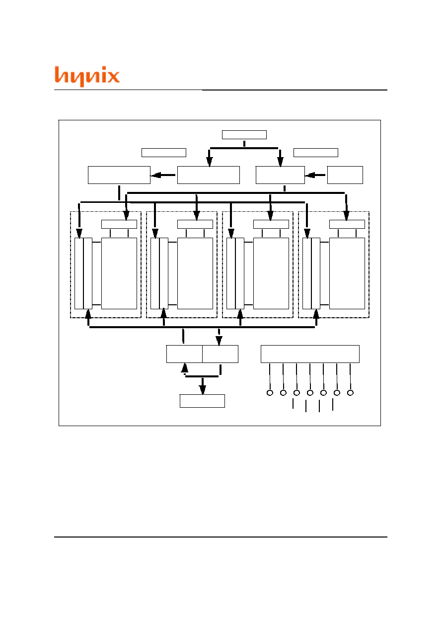
Block Diagram
A0 to A13
A0 to A8
A0 to A13
Column address
counter
Column address
buffer
Row address
counter
Refresh
counter
Input
buffer
Output
buffer
DQ0 to DQ7
Control logic &
timing generator
CLK
CKE
DQM
RAS
CAS
Row decoder
Memory array
Bank 0
4096 row
x 512 column
x 8 bit
Column decoder
Sense amplifier & I/O bus
Row decoder
Memory array
Bank 1
4096 row
x 512 column
x 8 bit
Column decoder
Sense amplifier & I/O bus
Row decoder
Memory array
Bank 2
4096 row
x 512 column
x 8 bit
Column decoder
Sense amplifier & I/O bus
Row decoder
Memory array
Bank 3
4096 row
x 512 column
x 8 bit
Column decoder
Sense amplifier & I/O bus
CS
WE
-2-
GM72V66841ET/ELT
Rev. 1.1/Apr.01
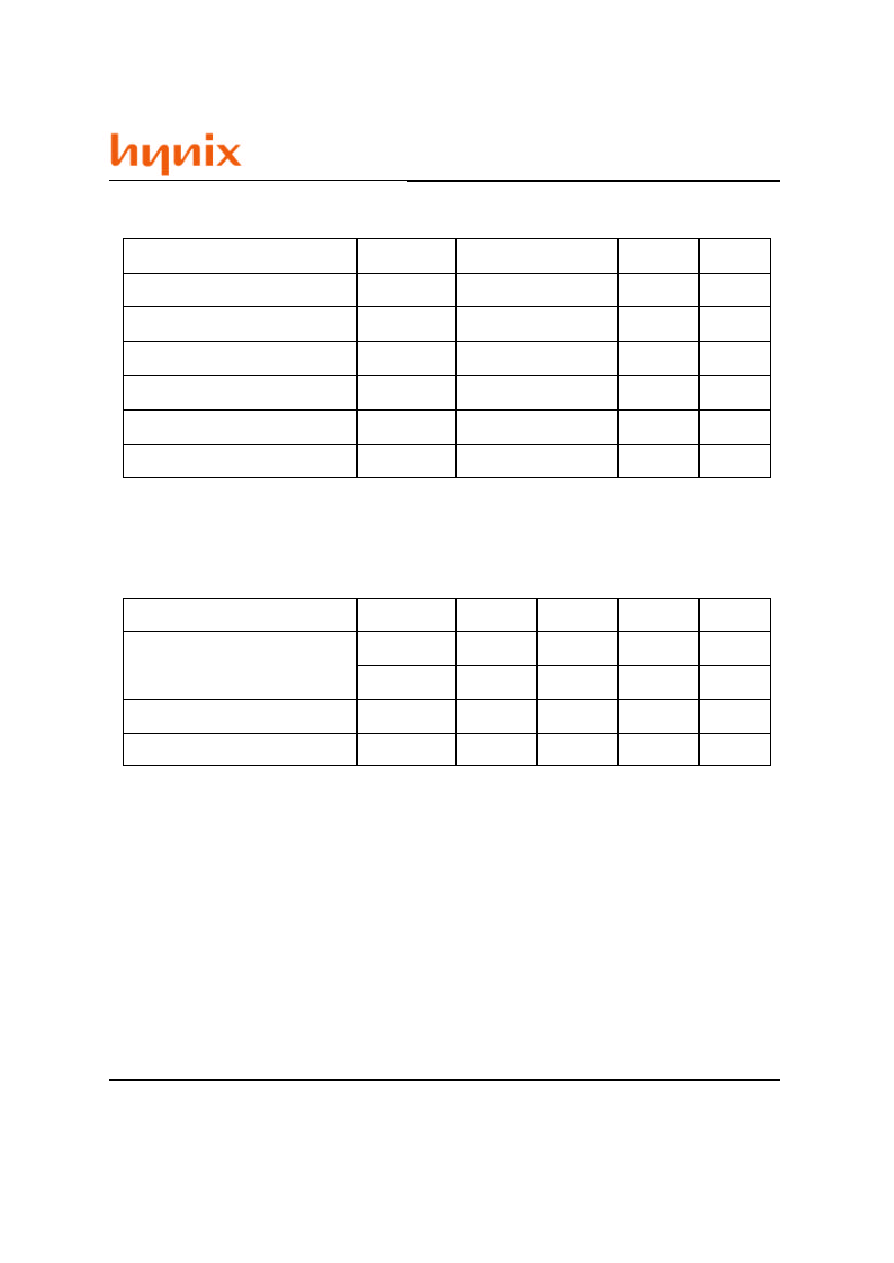
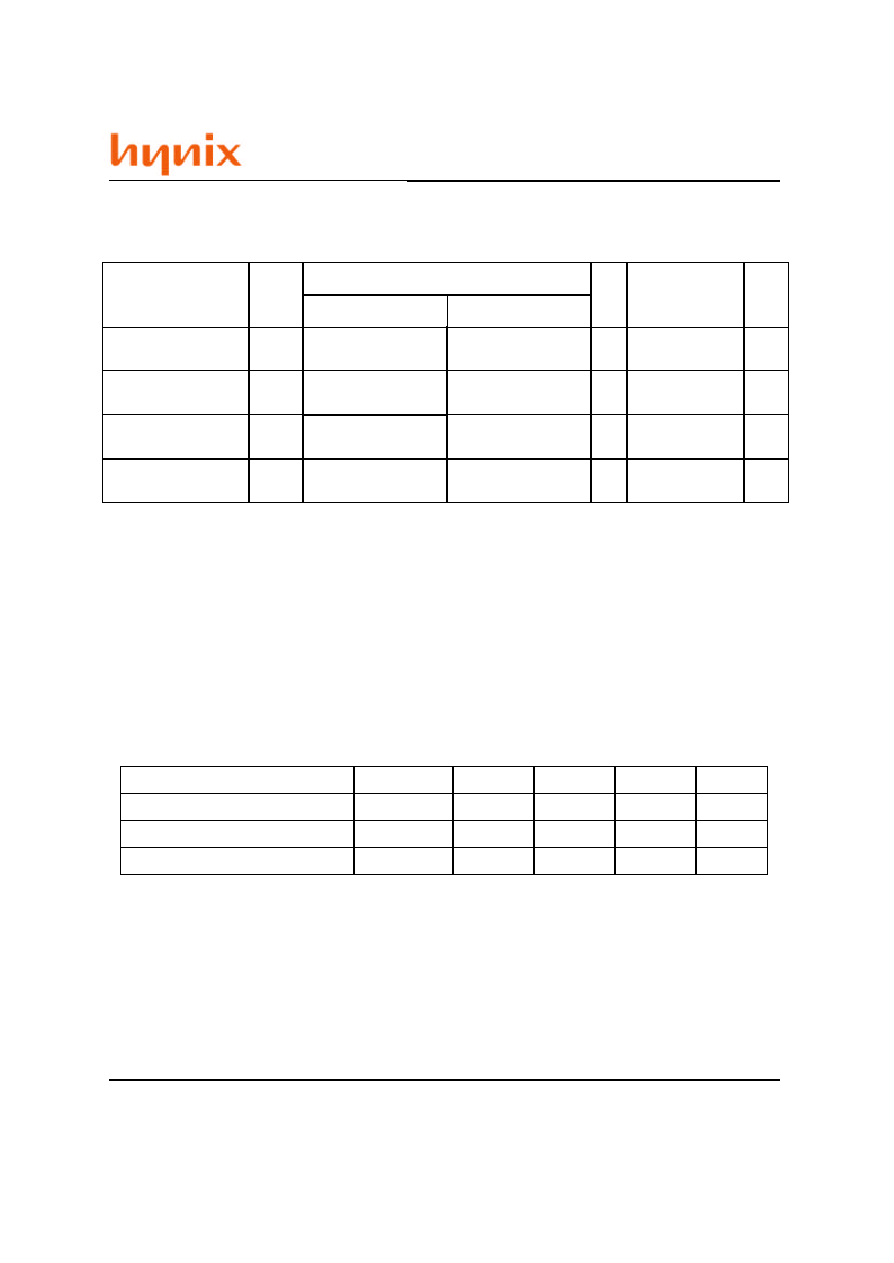
Absolute Maximum Ratings
Notes : 1. Respect to V
SS
Symbol
Value
Unit
Note
Parameter
V
T
-0.5 to Vcc+0.5
(<= 4.6 (max))
V
1
Voltage on any pin relative to V
SS
V
CC
-0.5 to +4.6
V
1
Supply voltage relative to V
SS
I
OUT
50
mA
Short circuit output current
P
T
1.0
W
Power dissipation
Topr
0 to +70
C
Operating temperature
Tstg
-55 to +125
C
Storage temperature
Notes : 1. All voltage referred to V
SS
.
2. V
IH
(max) = 5.6V for pulse width <= 3ns
3. V
IL
(min) = -2.0V for pulse width <= 3ns
Recommended DC Operating Conditions (Ta = 0 to + 70C)
Symbol
Min
Unit
Note
V
CC
, V
CCQ
V
1
V
SS
, V
SSQ
V
Input high voltage
V
IH
V
1, 2
Input low voltage
V
IL
V
1,3
Supply voltage
Parameter
Max
3.0
3.6
0
0
2.0
Vcc+0.3
-0.3
0.8
-3-
GM72V66841ET/ELT
Rev. 1.1/Apr.01
Notes : 1. I
CC
depends on output load condition when the device is selected. I
CC (
max) is specified at the
output open condition.
2. One bank operation.
3. Addresses are changed once per one cycle.
4. Addresses are changed once per two cycles.
5. After Power down mode, CLK operating current.
6. After Power down mode, no CLK operating current.
7. After self refresh mode set, self refresh current.
8. L-Version.
9. Input signals are V
I H
or V
IL
fixed.
Capacitance (Ta = 25C, V
CC
, V
CCQ
= 3.3 V +/-0.3 V)
Input leakage current
I
LI
uA
0 <=Vin <=V
CC
Output leakage current
I
LO
uA
0<=Vout<=V
CC
DQ = disable
Output high voltage
V
OH
V
I
OH
= -2 mA
Output low voltage
V
OL
V
I
OL
=2 mA
-1
1
-1.5
1.5
-
0.4
Parameter
Symbol
Unit Test conditions Notes
Min
Max
- 7, - 75, - 8, - 7K, - 7J
2.4
-
Notes : 1. Capacitance measured with Boonton Meter or effective capacitance measuring method.
2. DQM = V
I H
to disable Dout.
3. This parameter is sampled and not 100% tested.
4. Measured with 1.4 V bias and 200mV swing at the pin under measurement.
Parameter
Input capacitance (CLK)
Input capacitance (Signals)
Output capacitance (DQ)
Symbol
C
I1
C
I2
C
O
Min.
2.5
2.5
4.0
Max.
4
5
6.5
Unit
pF
pF
pF
Notes
1, 3, 4
1, 3, 4
1, 2, 3, 4
DC Characteristics (Ta = 0 to 70C, V
CC
, V
CCQ
= 3.3 V +/- 0.3 V, V
SS
, V
SSQ
= 0 V)
(Continued)
-5-