þÿ
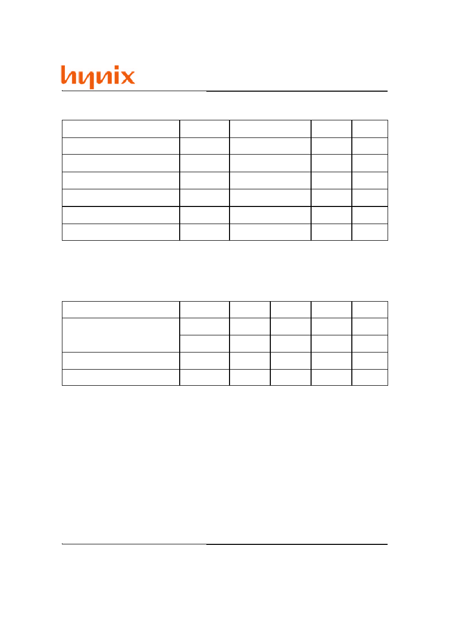
Description
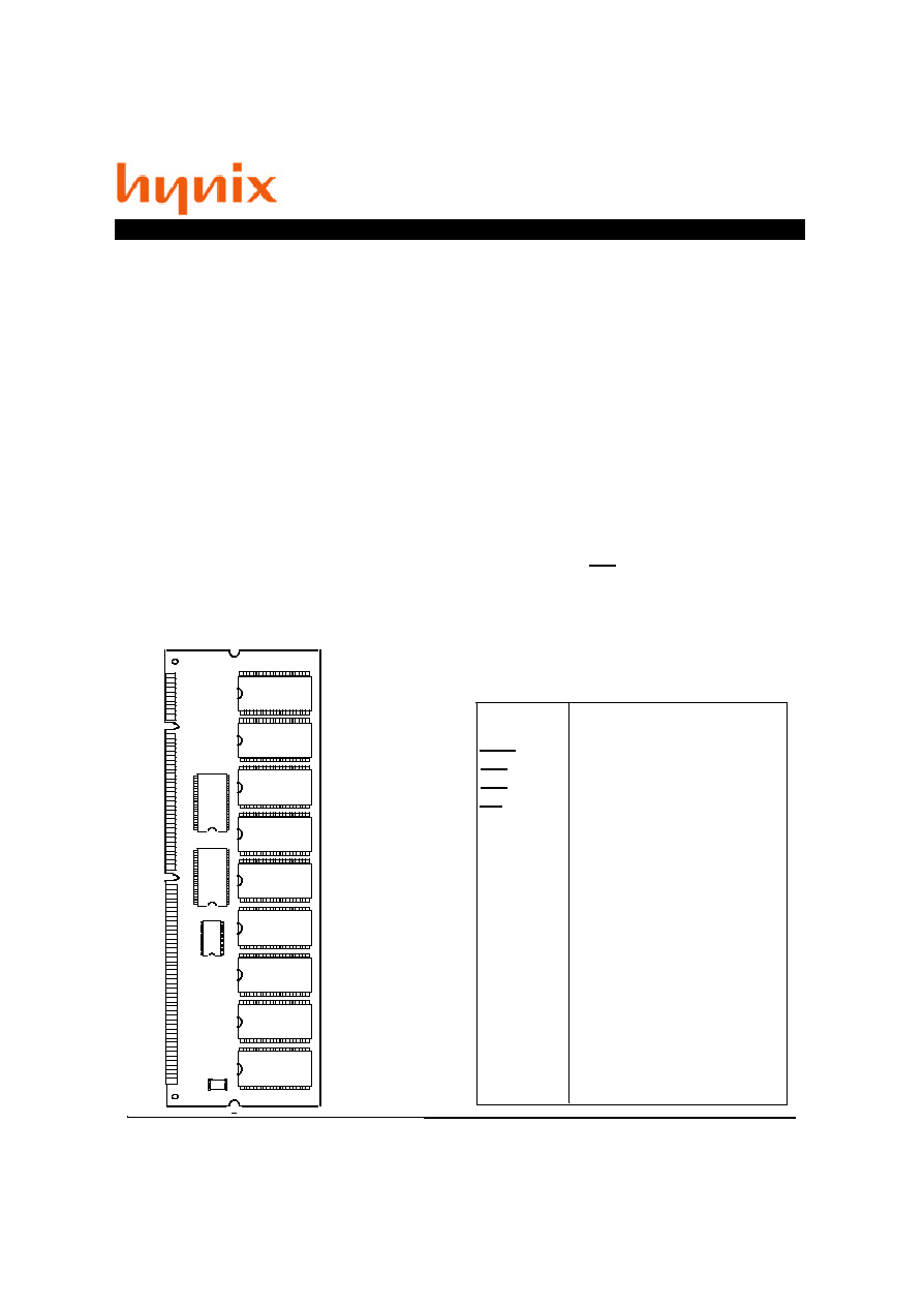
The GMM27316230ETG is a 16M x 72bits
Synchronous Dynamic RAM MODULE
which is assembled 18 pieces of 16M x 4bits
Synchronous DRAMs in 54 pin TSOP II, 2
pieces of 16 bits Register in 48 pin TSSOP,
one clock distribution PLL in 24 pin SOP and
one 2048 bit EEPROM in 8 pin TSSOP
package mounted on a 168 pin printed circuit
board with decoupling capacitors. The
G M M 2 7 3 1 6 2 3 0 E T G i s o p t i m i z e d f o r
application to the systems which are required
high density and large capacity such as main
memory of the computers and an image
memory systems, and to the others which are
requested compact size.
The GMM27316230ETG provides common
data inputs and outputs.
GMM27316230ETG (Double Side)
Features
Pin Name
CK0, 1, 2, 3
CKE0
S0, 2
RAS
CAS
WE
A0 ~ A11
BA0,1
REGE
DQ0 ~ 63
CB0 ~ 7
DQMB0 ~ 7
V
CC
V
SS
NC
V
REF
SDA
SCL
SA0 ~ 2
WP
DU
Clock input
Clock Enable
Chip Select
Row Address Strobe
Column Address Strobe
Write Enable
Address input
Bank Address input
Register Enable
Data input / output
Check Bits
Data input / output Mask
Power for internal circuit
Ground for internal circuit
No Connect
Power Supply for Reference
Serial Data input/ output
Serial Clock
Address in EEPROM
Write Protect for SPD
Don't Use
* PC133/PC100/PC66 Compatible
-7(143MHz)/-75(133MHz)/-8(125MHz)
-7K(PC100,2-2-2)/-7J(PC100,3-2-2)
* 3.3V ± 0.3V Power supply
* Maximum Clock frequency
100/125/133/143 MHz
* LVTTL Interface
* Burst read/write operation and burst read/
single write operation capability
* Programmable burst length ;
1, 2, 4, 8, Full page
* Programmable burst sequence
Sequential / Interleave
* Full Page burst length capability
Sequential burst
Burst stop capability
* Programmable CAS Latency ; 2, 3
* CKE power down mode
* Input / Output data masking
* 4096 Refresh Cycles / 64ms
* Auto refresh / Self refresh Capability
* Serial Presence Detect with EEPROM
-1-
16Mx72 bits
PC100/PC133 SDRAM Registered DIMM
based on 8Mx8 SDRAM with LVTTL, 4 banks & 4K Refresh
GMM27316230ETG
This document is a general product description and is subject to change without notice. Hynix semiconductor does not assume any
responsibility for use of circuits described. No patent licenses are implied.
Rev. 1.1/Apr.01
GMM27316230ETG
Rev. 1.1/Apr.01
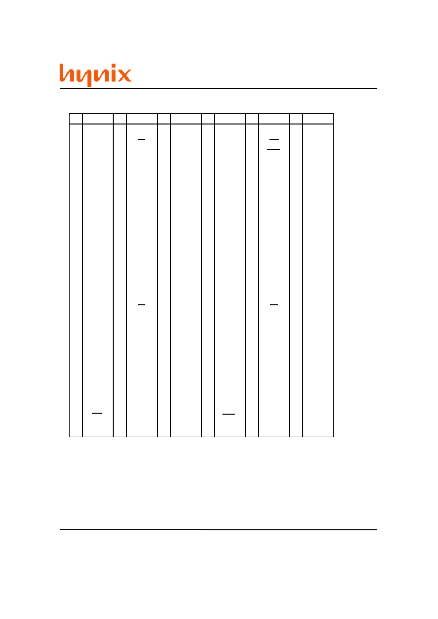
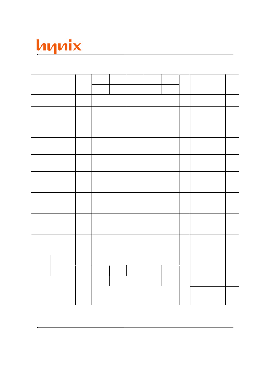
Pin
Symbol
1
2
3
4
5
6
7
8
9
10
11
12
13
14
15
16
17
18
19
20
21
22
23
24
25
26
27
28
Pin Configuration
Pin
Symbol
Pin
Symbol
Pin
Symbol
Pin
Symbol
Pin
Symbol
29
30
31
32
33
34
35
36
37
38
39
40
41
42
43
44
45
46
47
48
49
50
51
52
53
54
55
56
57
58
59
60
61
62
63
64
65
66
67
68
69
70
71
72
73
74
75
76
77
78
79
80
81
82
83
84
85
86
87
88
89
90
91
92
93
94
95
96
97
98
99
100
101
102
103
104
105
106
107
108
109
110
111
112
V
SS
DQ32
DQ33
DQ34
DQ35
V
CC
DQ36
DQ37
DQ38
DQ39
DQ40
V
SS
DQ41
DQ42
DQ43
DQ44
DQ45
V
CC
DQ46
DQ47
CB4
CB5
V
SS
NC
NC
V
CC
CAS
DQMB4
DQ18
DQ19
V
CC
DQ20
NC
*V
REF
, NC
*CKE1
V
SS
DQ21
DQ22
DQ23
V
SS
DQ24
DQ25
DQ26
DQ27
V
CC
DQ28
DQ29
DQ30
DQ31
V
SS
CK2
NC
WP
SDA
SCL
V
CC
DQMB1
S0
DU
V
SS
A0
A2
A4
A6
A8
A10/AP
BA1
V
CC
V
CC
CK0
V
SS
DU
S2
DQMB2
DQMB3
DU
V
CC
NC
NC
CB2
CB3
V
SS
DQ16
DQ17
113
114
115
116
117
118
119
120
121
122
123
124
125
126
127
128
129
130
131
132
133
134
135
136
137
138
139
140
DQMB5
*S1
RAS
V
SS
A1
A3
A5
A7
A9
BA0
A11
V
CC
CK1
*A12
V
SS
CKE0
*S3
DQMB6
DQMB7
*A13
V
CC
NC
NC
CB6
CB7
V
SS
DQ48
DQ49
141
142
143
144
145
146
147
148
149
150
151
152
153
154
155
156
157
158
159
160
161
162
163
164
165
166
167
168
DQ50
DQ51
V
CC
DQ52
NC
*V
REF
, NC
REGE
V
SS
DQ53
DQ54
DQ55
V
SS
DQ56
DQ57
DQ58
DQ59
V
CC
DQ60
DQ61
DQ62
DQ63
V
SS
CK3
NC
SA0
SA1
SA2
V
CC
V
SS
DQ0
DQ1
DQ2
DQ3
V
CC
DQ4
DQ5
DQ6
DQ7
DQ8
V
SS
DQ9
DQ10
DQ11
DQ12
DQ13
V
CC
DQ14
DQ15
CB0
CB1
V
SS
NC
NC
V
CC
WE
DQMB0
* These pins are not used in this module
-2-
GMM27316230ETG
Rev. 1.1/Apr.01
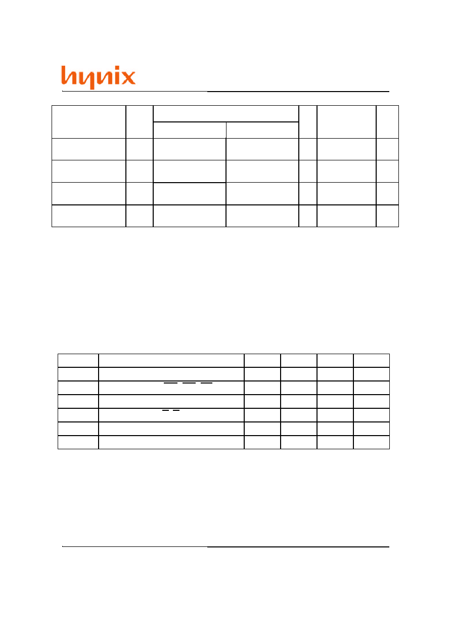
Block Diagram
V
CC
V
SS
Capacitor
one 0.0022uF and one 0.22uF per SDRAM
A0
A1
A2
SA2
Serial PD
SDA
SCL
U0 ~ U17
U0 ~ U17
Vss
WP
47kohm
CK1,2,3
12pF
10ohm
REGE
Vcc
10kohm
A0 ~ A11, BA0,1
RAS
CAS
CKE0, DQMB0~7
WE
U0 - U17
U0 - U17
U0 - U17
U0 - U17
U0 - U17
Register
S0,2
U0 - U17
DQ0
DQ1
DQ2
DQ3
U0
U1
U2
U3
U9
U10
U11
U12
DQM CS
DQM CS
DQM CS
DQM CS
DQM CS
DQM CS
DQM CS
DQM CS
DQMB0
DQMB1
DQMB4
DQMB5
U5
U6
U7
U8
DQM CS
DQM CS
DQM CS
DQM CS
S2
DQMB2
DQMB3
DQM CS
DQM CS
U4
U13
S0
DQ4
DQ5
DQ6
DQ7
DQ8
DQ9
DQ10
DQ11
DQ12
DQ13
DQ14
DQ15
CB0
CB1
CB2
CB3
DQ16
DQ17
DQ18
DQ19
DQ20
DQ21
DQ22
DQ23
DQ24
DQ25
DQ26
DQ27
DQ28
DQ29
DQ30
DQ31
DQ0
DQ1
DQ2
DQ3
DQ0
DQ1
DQ2
DQ3
DQ0
DQ1
DQ2
DQ3
DQ0
DQ1
DQ2
DQ3
DQ0
DQ1
DQ2
DQ3
DQ0
DQ1
DQ2
DQ3
DQ0
DQ1
DQ2
DQ3
DQ0
DQ1
DQ2
DQ3
DQ0
DQ1
DQ2
DQ3
DQ32
DQ33
DQ34
DQ35
DQ36
DQ37
DQ38
DQ39
DQ40
DQ41
DQ42
DQ43
DQ44
DQ45
DQ46
DQ47
CB4
CB5
CB6
CB7
DQ0
DQ1
DQ2
DQ3
DQ0
DQ1
DQ2
DQ3
DQ0
DQ1
DQ2
DQ3
DQ0
DQ1
DQ2
DQ3
DQ0
DQ1
DQ2
DQ3
U14
U15
U16
U17
DQM CS
DQM CS
DQM CS
DQM CS
DQMB6
DQMB7
DQ48
DQ49
DQ50
DQ51
DQ52
DQ53
DQ54
DQ55
DQ56
DQ57
DQ58
DQ59
DQ60
DQ61
DQ62
DQ63
DQ0
DQ1
DQ2
DQ3
DQ0
DQ1
DQ2
DQ3
DQ0
DQ1
DQ2
DQ3
DQ0
DQ1
DQ2
DQ3
PLL
CK0
3 SDRAMS
3 SDRAMS
3 SDRAMS
3 SDRAMS
3 SDRAMS
3 SDRAMS
2 Registers
12pF
PCK
SA0 SA1
-3-
GMM27316230ETG
Rev. 1.1/Apr.01
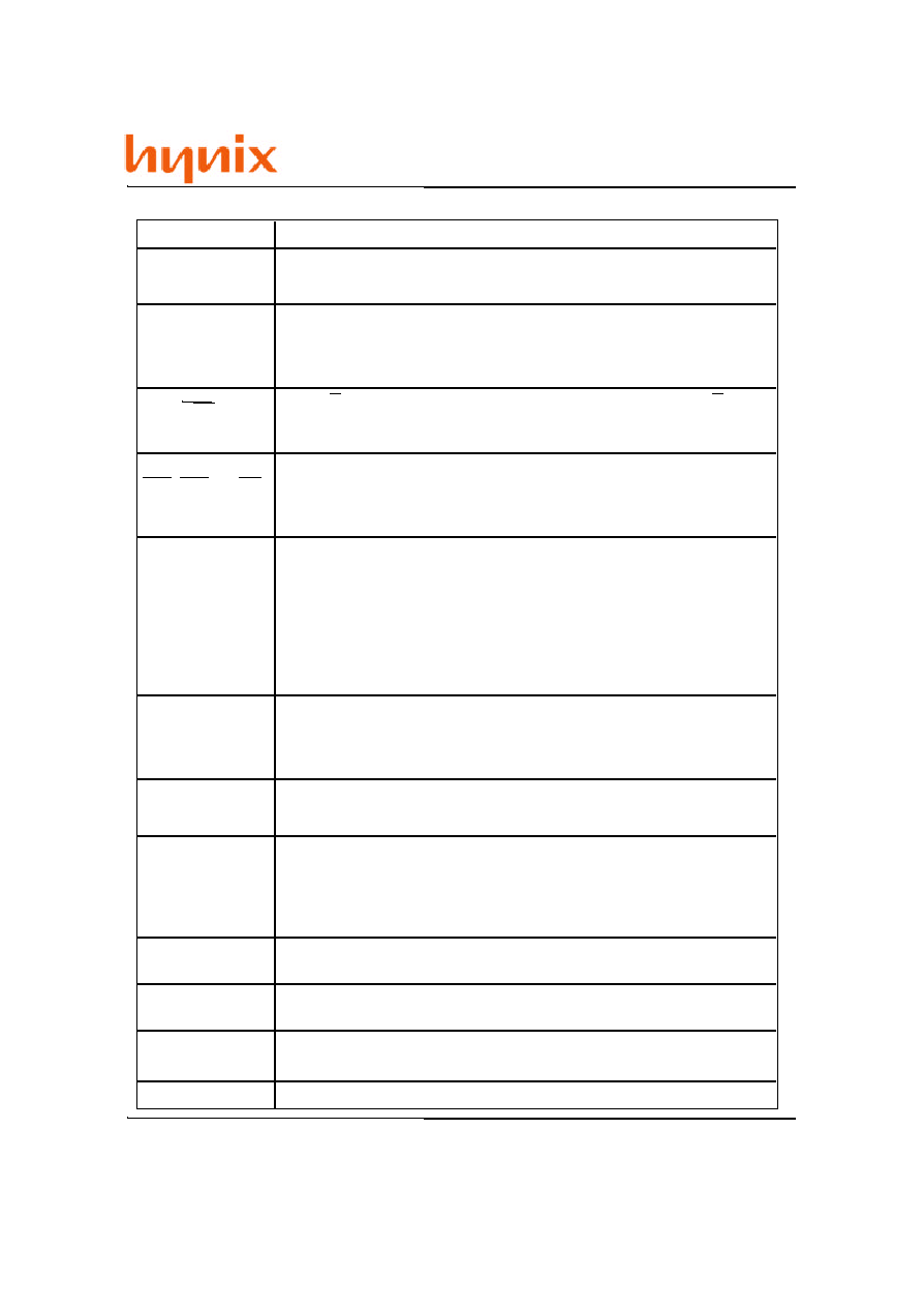
Pin Description
Pin Name
DESCRIPTION
CK0, 1, 2, 3
(input pins)
CK is the master clock input to this pin. The other input signals are
referred at CK rising edge.
CKE0
(input pin)
This pin determines whether or not the next CK is valid. If CKE is
High, the next CK rising edge is valid. If CKE is Low, the next CK
rising edge is invalid. This pin is used for power-down and clock
suspend modes.
When S is Low, the command input cycle becomes valid. When S is
high, all inputs are ignored. However, internal operations (bank active,
burst operations, etc.) are held.
S0, 2
(input pins)
Although these pin names are the same as those of conventional
DRAMs, they function in a different way. These pins define operation
commands (read, write, etc.) depending on the combination of their
voltage levels. For details, refer to the command operation section.
RAS, CAS and WE
(input pins)
A0 ~ A11
(input pins)
Row address (AX0 to AX11) is determined by A0 to A11 level at the
bank active command cycle CK rising edge. Column address is
determined by A0 to A8 level at the read or write command cycle CK
rising edge. And this column address becomes burst access start
address. A10 defines the precharge mode. When A10 = High at the
precharge command cycle, both banks are precharged. But when A10 =
Low at the precharge command cycle, only the bank that is selected by
BA0 is precharged.
BA0,1
(input pin)
BA0,1 are bank select signal. If BA0 is Low and BA1 is High, bank 0 is
selected. If BA0 is High and BA1 is Low, bank 1 is selected. If BA0 is
Low and BA1 is High, bank 2 is selected. If BA0 is High and BA1 is
High, bank 3 is selected.
DQ0 ~ DQ63
CB0 ~ CB7
(I/O pins)
Data is input and output from these pins. These pins are the same as
those of a conventional DRAMs. Data is not latched in the register.
DQMB0 ~ DQMB7
(input pins)
DQMB controls input/output buffers.
*Read operation: If DQMB is High, The output buffer becomes High-Z.
If the DQMB is Low, the output buffer becomes Low-Z.
*Write operation: If DQMB is High, the previous data is held (the new data
is not written). If DQMB is Low, the data is written.
V
CC
(power supply pins)
3.3 V is applied. (V
CC
is for the internal circuit)
V
SS
(power supply pins)
Ground is connected. (V
SS
is for the internal circuit)
NC
No Connection pins.
REGE
If REGE input is high, permits the DIMM to operate in `registered mode`.
If REGE input is low, permits the DIMM to operate in `buffered mode`.
-4-
GMM27316230ETG
Rev. 1.1/Apr.01
Registered DIMM Operation
1. All control and address signals are registered on-DIMM register and hence delayed by one cycle in
arriving at the SDRAMs. But data is not registered in the register.
2. CAS latency defines the delay from when a READ command is registered on a rising clock edge to
when the data from that READ command becomes available at the outputs. Do not confuse DIMM
CAS latency with the SDRAM CAS latency which is one clock less.
Absolute Maximum Ratings
Notes : 1. Respect to V
SS
Symbol
Value
Unit
Note
Parameter
V
T
-0.5 to Vcc+0.5
(<= 4.6 (max))
V
1
Voltage on any pin relative to V
SS
V
CC
-0.5 to +4.6
V
1
Supply voltage relative to V
SS
I
OUT
50
mA
Short circuit output current
P
T
1.0
W
Power dissipation
Topr
0 to +70
C
Operating temperature
Tstg
-55 to +125
C
Storage temperature
Notes : 1. All voltage referred to V
SS
.
2. V
IH
(max) = 5.6V for pulse width <= 3ns
3. V
IL
(min) = -2.0V for pulse width <= 3ns
Recommended DC Operating Conditions (Ta = 0 to + 70C)
Symbol
Min
Unit
Note
V
CC
, V
CCQ
V
1
V
SS
, V
SSQ
V
Input high voltage
V
IH
V
1, 2
Input low voltage
V
IL
V
1,3
Supply voltage
Parameter
Max
3.0
3.6
0
0
2.0
Vcc+0.3
-0.3
0.8
-5-
GMM27316230ETG
Rev. 1.1/Apr.01
DC Characteristics (Ta = 0 to 70C, V
CC
, V
CCQ
= 3.3 V +/- 0.3 V, V
SS
, V
SSQ
= 0 V)
Parameter
Symbol
Unit Test conditions Notes
Operating
current
Standby current in
power down
I
CC2P
Self refresh current
I
CC6
mA
V
IH
>=V
CC
- 0.2
V
IL
<=0.2V
7
Burst length= 1
t
RC
= min
1, 2, 3
CKE = V
IL
,
t
CK
= 12 ns
5
I
CC1
mA
mA
Standby current in
power down
(input signal stable)
I
CC2PS
CKE=V
IL
,
t
CK
= infinity
6
mA
Standby current in
non power down
(CAS Latency=2)
I
CC2N
CKE,CS = V
IH
,
t
CK
= 12ns
4
mA
Standby current in
non power down
(input signal stable)
I
CC2NS
CKE = V
IH
,
t
CK
= infinity
4
mA
Active standby current
in power down
I
CC3P
CKE = V
IL
,
t
CK
= 12 ns,
DQ = High-Z
1,2,5
mA
Active standby current
in power down
(input signal stable)
I
CC3PS
CKE = V
IL
,
t
CK
= infinity
2,6
mA
Active standby current
in non power down
I
CC3N
CKE,CS = V
IH
,
t
CK
= 12 ns,
DQ = High-Z
1,2,4
mA
Active standby current
in non power down
(input signal stable)
I
CC3NS
CKE = V
IH
,
t
CK
= infinity
2,8
mA
Burst
operating
current
I
CC4
t
CK
= min
BL = 4
1,2,3
mA
( CL= 2 )
I
CC4
mA
( CL= 3 )
Refresh current
t
RC
= min
3
I
CC5
mA
- 8
Max
Max
-7J
1200
350
- 75
Max
1300
Max
-7K
- 7
Max
18
40
40
280
80
110
80
1600
550
1800
1500
1600
1500
1800
1600
1600
1500
1800
1600
-6-
GMM27316230ETG
Rev. 1.1/Apr.01
Notes : 1. I
CC
depends on output load condition when the device is selected. I
CC (
max) is specified at the
output open condition.
2. One bank operation.
3. Addresses are changed once per one cycle.
4. Addresses are changed once per two cycles.
5. After Power down mode, CLK operating current.
6. After Power down mode, no CLK operating current.
7. After self refresh mode set, self refresh current.
8. Input signals are V
I H
or V
IL
fixed.
Input leakage current
I
LI
uA
0 <=Vin <=V
CC
Output leakage current
I
LO
uA
0<=Vout<=V
CC
DQ = disable
Output high voltage
V
OH
V
I
OH
= -2 mA
Output low voltage
V
OL
V
I
OL
=2 mA
-1
1
-1.5
1.5
-
0.4
Parameter
Symbol
Unit Test conditions Notes
Min
Max
- 7, - 75, - 8, - 7K, - 7J
2.4
-
Capacitance (Ta = 25C, V
CC
, V
CCQ
= 3.3V +/- 0.3V)
Note : 1. Capacitance measured with Boonton Meter or effective capacitance measuring method.
2. DQMB = V
IH
to disable Dout.
3. This parameter is sampled and not 100% tested.
Symbol
Parameter
Min
Max
Unit
Notes
C
I1
Input capacitance (A0 ~ A11, BA0, BA1)
7
10
pF
1, 3
C
I2
Input capacitance (RAS, CAS, WE, CKE0)
13
pF
C
I3
Input capacitance (CK0, CK1, CK2, CK3)
15
pF
C
I4
Input capacitance (S0,S2)
6
pF
C
I/O
I/O capacitance (DQ0 ~ 63, CB0 ~ 7)
10
pF
18
35
10
14
1, 3
1, 3
1, 3
1, 2, 3
C
I6
Input capacitance (DQMB0,1,2,3,4,5,6,7)
6
pF
10
1, 3
-7-
GMM27316230ETG
Rev. 1.1/Apr.01
AC Characteristics (Ta = 0 to 70C, V
CC
, V
CCQ
= 3.3 V +/- 0.3 V, V
SS
, V
SSQ
= 0 V)
Symbol
Unit Notes
t
CK
t
CK
Parameter
System clock
cycle time
(CL=2)
(CL=3)
ns
1
t
CKH
ns
1
CLK high pulse width
t
CKL
ns
1
CLK low pulse width
t
AC
t
AC
Access time
from CLK
(CL=2)
(CL=3)
ns
1, 2
t
OH
ns
1, 2
Data-out hold time
t
LZ
ns
1, 2, 3
CLK to Data-out low
impedance
t
HZ
CLK to Data-out
high impedance
( CL = 2,3 )
ns
1, 4
t
DS
ns
1
Data-in setup time
t
DH
ns
1
Data-in hold time
t
AS
ns
1
Address setup time
t
AH
ns
1
Address hold time
t
CES
ns
1, 5
CKE setup time
t
CESP
ns
1
CKE setup time for
power down exit
t
CEH
ns
1
CKE hold time
t
CS
ns
1
Command (CS, RAS,
CAS, WE, DQM)
setup time
t
RC
ns
1
Ref/Active to Ref/Active
command period
t
CH
ns
1
Command (CS, RAS,
CAS, WE, DQM)
hold time
t
RAS
ns
1
Active to Precharge
command period
t
RCD
ns
1
Active command to
column command
(same bank)
t
RP
ns
1
Precharge to active
command period
- 7K
Min Max
10
-
10
-
3
-
3
-
-
6
-
6
3
-
2
-
-
6
2
-
1
-
2
-
1
-
2
-
2
-
1
-
2
-
70
-
1
-
50
120000
20
-
20
-
- 7J
Min Max
10
-
15
-
3
-
3
-
-
6
-
8
3
-
2
-
-
6
2
-
1
-
2
-
1
-
2
-
2
-
1
-
2
-
70
-
1
-
50
120000
20
-
20
-
- 8
Min Max
8
-
10
-
3
-
3
-
-
6
-
6
3
-
2
-
-
6
2
-
1
-
2
-
1
-
2
-
2
-
1
-
2
-
68
-
1
-
48
120000
20
-
20
-
- 75
Min Max
7.5
-
10
-
2.5
-
2.5
-
-
5.4
-
6
2.7
-
1.5
-
-
5.4
1.5
-
0.8
-
1.5
-
0.8
-
1.5
-
1.5
-
0.8
-
1.5
-
65
-
0.8
-
45
120000
20
-
20
-
- 7
Min Max
7
-
10
-
2.5
-
2.5
-
-
5.4
-
6
2.7
-
1.5
-
-
5.4
1.5
-
0.8
-
1.5
-
0.8
-
1.5
-
1.5
-
0.8
-
1.5
-
62
-
0.8
-
42
120000
20
-
20
-
-8-
GMM27316230ETG
Rev. 1.1/Apr.01
AC Characteristics (Ta = 0 to 70C, V
CC
, V
CCQ
= 3.3 V +/-0.3 V, V
SS
, V
SSQ
= 0 V)
(Continued)
Notes : 1. AC measurement assumes
t
T
= 1ns. Reference level for timing of input signals is 1.40V.
If
t
T
is longer than 1ns,transition time compensation should be considered.
2. Access time is measured at 1.40V. Load condition is C
L
= 50pF without termination.
3.
t
LZ
(min)defines the time at which the outputs achieves the low impedance state.
4.
t
HZ
(max)defines the time at which the outputs achieves the high impedance state.
5.
t
CES
define CKE setup time to CKE rising edge except Power down exit command.
6. The on-DIMM PLL must be given enough clock cycles to stabilize (
t
STAB
) before any
operation can be guaranteed.
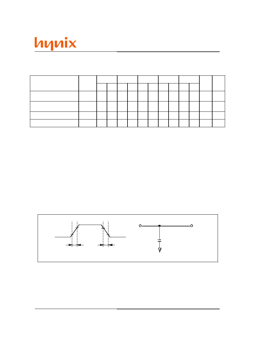
Test Condition
· Input and output-timing reference levels: 1.4V
· Input waveform and output load: See following figures
20%
t
T
t
T
0.4V
2.4V
I/O
80%
OPEN
input
C
L
Symbol
Notes
Parameter
1
t
RRD
1
Active (a) to Active (b)
command period
t
REF
Refresh period
t
RWL
Write recovery or data-in
to precharge lead time
Unit
ns
ns
ms
- 8
Min Max
8
-
16
-
-
64
- 7K
Min Max
10
-
20
-
-
64
- 7J
Min Max
10
-
20
-
-
64
- 75
Min Max
7.5
-
15
-
-
64
- 7
Min Max
7
-
14
-
-
64
t
STAB
us
6
PLL Stabilization time
200
-
200
-
200
-
200
-
200
-
-9-
GMM27316230ETG
Rev. 1.1/Apr.01
Relationship Between Frequency and Minimum Latency
Notes
l
RCD
1
Active command to column
command (same bank)
l
RC
= [
l
RAS
+
l
RP
], 1
Active command to active
command (same bank)
l
RAS
Active command to Precharge
command (same bank)
l
RP
1
Precharge command to active
command (same bank)
l
RWL
1
Write recovery or last data-in to
Precharge command
(same bank)
l
RRD
1
Active command to active
command (different bank)
l
SREX
Self refresh exit time
l
APW
= [
l
RWL
+
l
RP
], 1
Last data in to active command
(Auto Precharge, same bank)
l
SEC
= [
l
RC
]
Self refresh exit to command
input
l
HZP
Precharge
command to
high impedance
l
HZP
(CL=2)
(CL=3)
l
APR
Last data out to active
command
(auto Precharge) (same bank)
l
EP
Last data out to
Precharge
(early Precharge)
l
EP
(CL=2)
(CL=3)
l
CCD
Column command to column
command
l
WCD
Write command to data in
latency
l
DID
DQM to data in
l
DOD
DQM to data out
l
PEC
Power down exit to command
input
l
CLE
CKE to CLK disable
l
RSA
Register set to active command
l
CDD
Parameter
t
CK
(ns)
frequency(MHz)
1
CS to command disable
Symbol
-7J
100
2
7
5
10
2
1
2
1
3
7
-
3
1
-
- 2
1
0
0
2
1
1
1
0
-75
133
3
9
6
7.5
3
1
2
1
4
9
-
3
1
-
-2
1
0
0
2
1
1
1
0
-8
125
3
9
6
8
3
1
2
1
4
9
-
3
1
-
-2
1
0
0
2
1
1
1
0
100
2
7
5
10
2
1
2
2
3
7
2
3
1
-1
-2
1
0
0
2
1
1
1
0
66
2
6
4
15
2
1
2
2
3
6
2
3
1
-1
- 2
1
0
0
2
1
1
1
0
-7
143
3
9
6
7
3
1
2
1
4
9
-
3
1
-
-2
1
0
0
2
1
1
1
0
100
2
7
5
10
2
1
2
1
3
7
2
3
1
- 1
- 2
1
0
0
2
1
1
1
0
-7K
100
2
7
5
10
2
1
2
1
3
7
2
3
1
-1
-2
1
0
0
2
1
1
1
0
100
2
7
5
10
2
1
2
1
3
7
2
3
1
-1
-2
1
0
0
2
1
1
1
0
100
2
7
5
10
2
1
2
1
3
7
2
3
1
- 1
- 2
1
0
0
2
1
1
1
0
-10-
GMM27316230ETG
Rev. 1.1/Apr.01
Relationship Between Frequency and Minimum Latency
Notes : 1.
l
RCD
to
l
RRD
are recommended value.
Symbol
Notes
l
BSR
Burst stop to
output valid
data hold
l
BSR
(CL=2)
(CL=3)
l
BSH
Burst stop to
output high
impedance
l
BSH
(CL=2)
(CL=3)
l
BSW
Burst stop to write data ignore
Parameter
t
CK
(ns)
frequency(MHz)
- 7K
- 7J
-7
143
7
-
2
-
3
0
- 8
125
8
-
2
-
3
0
100
10
1
2
2
3
0
100
10
-
2
-
3
0
66
15
1
2
2
3
0
-75
133
7.5
-
2
-
3
0
100
10
1
2
2
3
0
100
10
1
2
2
3
0
100
10
1
2
2
3
0
100
10
1
2
2
3
0
-11-
GMM27316230ETG
Rev. 1.1/Apr.01
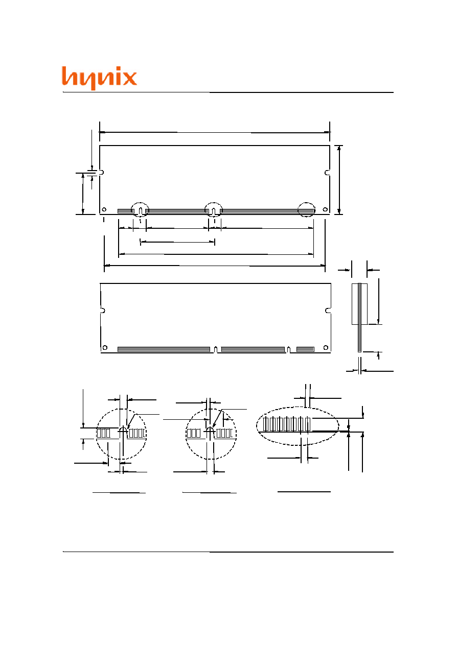
Package Dimension
NOTE : 1. Tolerances on all dimensions ±5 (0.127) unless otherwise specified.
2. Thickness includes Plating and / or Metallization.
85
168
1
84
5250(133.35)
5013.78(127.35)
1700(43.18)
1450(36.83)
2150(54.61)
450(11.43)
250(6.35)
700(17.78)
157.48(4.0)
1650(41.91)
"C"
"B"
"A"
4550(115.57)
DETAIL "B"
DETAIL "A"
5.9(0.15)
100(2.54)
min.
39.37(1.0)
50(1.27)
78.74(2.0)
39.37(1.0)
DETAIL "C"
78.74(2.0)
122.83(3.12)
39.37(1.0)
125(3.175)
125(3.175)
Unit: mil (mm)
* (1 mil = 1/1000 inches)
R78.74
(2.0)
R78.74
(2.0)
(Front Side)
(Rear Side)
50(1.27)
157.48(4.0)
min.
157.48(4.0) max.
-12-