738280T
Description
Features
1
GMM7738280CTG-5/6
8,388,608 WORDS x 72 BIT
CMOS DYNAMIC RAM MODULE
GMM7738280CTG (Double Side)
Note : Pins Marked
*
are not used in this module.
* This Data Sheet is subject to change without notice.
* 168 pins Dual In-Line Package
- GMM7738280CTG : Gold plating
* Extended Data Ouput (EDO) Mode Capability
* Single Power Supply
* Fast Access Time & Cycle Time
* Low Power
Active : 4770/4446mW (MAX)
Standby : 89mW (CMOS level : MAX)
* RAS Only Refresh, CAS before RAS Refresh,
Hidden Refresh Capability
* All inputs and outputs TTL Compatible
* 4096 Refresh Cycles/64ms
(Unit: ns)
GMM7738280CTG -5
t
RAC
t
CAC
t
RC
t
HPC
50
60
20
104
25
GMM7738280CTG -6
Speed
Pin Symbol Pin Symbol Pin Symbol
1
2
3
4
5
6
7
8
9
10
11
12
13
14
15
16
17
18
19
20
21
22
23
24
25
26
27
28
57
58
59
60
61
62
63
64
65
66
67
68
69
70
71
72
73
74
75
76
77
78
79
80
81
82
83
84
Pin Symbol
85
86
87
88
89
90
91
92
93
94
95
96
97
98
99
100
101
102
103
104
105
106
107
108
109
110
111
112
V
SS
DQ
0
DQ
1
DQ
2
DQ
3
V
CC
DQ
4
DQ
5
DQ
6
DQ
7
DQ
8
V
SS
DQ
9
DQ
10
DQ
11
DQ
12
DQ
13
V
CC
DQ
14
DQ
15
DQ
16
DQ
17
V
SS
RSVD
RSVD
V
CC
/WE
0
/CAS
0
V
SS
DQ
36
DQ
37
DQ
38
DQ
39
V
CC
DQ
40
DQ
41
DQ
42
DQ
43
DQ
44
V
SS
DQ
45
DQ
46
DQ
47
DQ
48
DQ
49
V
CC
DQ
50
DQ
51
DQ
52
DQ
53
V
SS
RSVD
RSVD
V
CC
RFU
/CAS
1*
DQ
22
DQ
23
V
cc
DQ
24
RFU
RFU
RFU
RFU
DQ
25
DQ
26
DQ
27
V
SS
DQ
28
DQ
29
DQ
30
DQ
31
V
CC
DQ
32
DQ
33
DQ
34
DQ
35
V
SS
PD
1
PD
3
PD
5
PD
7
ID
0
V
CC
RSVD
/RAS
0
/OE
0
V
SS
A
0
A
2
A
4
A
6
A
8
A
10
RSVD
V
CC
RFU
RFU
V
SS
/OE
2
/RAS
2
/CAS
4
RSVD
/WE
2
V
CC
RSVD
RSVD
DQ
18
DQ
19
V
SS
DQ
20
DQ
21
Pin Configuration (Top View)
Pin Symbol
113
114
115
116
117
118
119
120
121
122
123
124
125
126
127
128
129
130
131
132
133
134
135
136
137
138
139
140
RSVD
/RAS
1*
RFU
V
SS
A
1
A
3
A
5
A
7
A
9
A
11
A
13*
V
CC
RFU
B
0
V
SS
RFU
/RAS
3*
/CAS
5*
RSVD
/PDE
V
CC
RSVD
RSVD
DQ
54
DQ
55
V
SS
DQ
56
DQ
57
Pin Symbol
141
142
143
144
145
146
147
148
149
150
151
152
153
154
155
156
157
158
159
160
161
162
163
164
165
166
167
168
DQ
58
DQ
59
V
CC
DQ
60
RFU
RFU
RFU
RFU
DQ
61
DQ
62
DQ
63
V
SS
DQ
64
DQ
65
DQ
66
DQ
67
V
CC
DQ
68
DQ
69
DQ
70
DQ
71
V
SS
PD
2
PD
4
PD
6
PD
8
ID
1
V
CC
The GMM7738280CTG is an 8M x 72 bits
Dynamic RAM MODULE which is assembled 9
pieces of 8M x 8bit DRAMs in 32 pin TSOP II
package and two 16bit driver ICs in 48pin
TSSOP package mounted on a 168 pin printed
circuit board with decoupling capacitors.
The GMM7738280CTG is optimized for
application to the systems which are required
high density and large capacity such as main
memory of the computers and an image memory
systems, and to the others which are requested
compact size.
The GMM7738280CTG provides common data
inputs and Extended Data Outputs.
29
30
31
32
33
34
35
36
37
38
39
40
41
42
43
44
45
46
47
48
49
50
51
52
53
54
55
56
18
84
20
LG Semicon
GMM7738280CTG-5/6
2
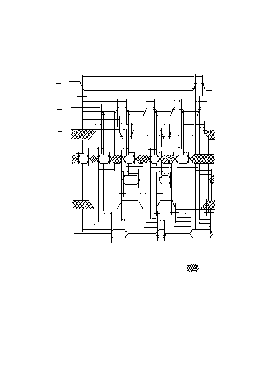
Block Diagram
DQ 0
DQ 40
DQ 41
DQ 42
DQ 43
DQ 44
DQ 45
DQ 46
DQ 47
DQ 64
DQ 65
DQ 66
DQ 67
DQ 68
DQ 69
DQ 70
DQ 71
DQ 1
DQ 2
DQ 3
DQ 4
DQ 5
DQ 6
DQ 7
DQ 8
DQ 9
DQ 10
DQ 11
DQ 12
DQ 13
DQ 14
DQ 15
DQ 16
DQ 17
DQ 18
DQ 19
DQ 20
DQ 21
DQ 22
DQ 23
DQ 24
DQ 25
DQ 26
DQ 27
DQ 28
DQ 29
DQ 30
DQ 31
DQ 32
DQ 33
DQ 34
DQ 35
DRAMS: D0~D8
A1~A11
A0
B0
DRAMS: D0~D4
DRAMS: D5~D8
VSS
PDE
(when= 0, 1= NC)
V
CC
V
SS
0.22uF Capacitor
D0~D8, Buffer
D0~D8, Buffer
OE0
WE0
CAS0
RAS0
A0~A12,B0
CAS4
RAS2
OE2
WE2
D0
DQ 4
DQ 0
DQ 1
DQ 2
DQ 3
DQ 5
DQ 6
DQ 7
D1
DQ 4
DQ 0
DQ 1
DQ 2
DQ 3
DQ 5
DQ 6
DQ 7
D2
DQ 4
DQ 0
DQ 1
DQ 2
DQ 3
DQ 5
DQ 6
DQ 7
D3
DQ 4
DQ 0
DQ 1
DQ 2
DQ 3
DQ 5
DQ 6
DQ 7
D4
DQ 4
DQ 0
DQ 1
DQ 2
DQ 3
DQ 5
DQ 6
DQ 7
DQ 36
DQ 37
DQ 38
DQ 39
D5
DQ 4
DQ 0
DQ 1
DQ 2
DQ 3
DQ 5
DQ 6
DQ 7
DQ 48
DQ 49
DQ 50
DQ 51
DQ 52
DQ53
DQ 54
DQ 55
D6
DQ 4
DQ 0
DQ 1
DQ 2
DQ 3
DQ 5
DQ 6
DQ 7
D8
DQ 4
DQ 0
DQ 1
DQ 2
DQ 3
DQ 5
DQ 6
DQ 7
DQ 56
DQ 57
DQ 58
DQ 59
DQ 60
DQ 61
DQ 62
DQ63
D7
DQ 4
DQ 0
DQ 1
DQ 2
DQ 3
DQ 5
DQ 6
DQ 7
LG Semicon
GMM7738280CTG-5/6
3
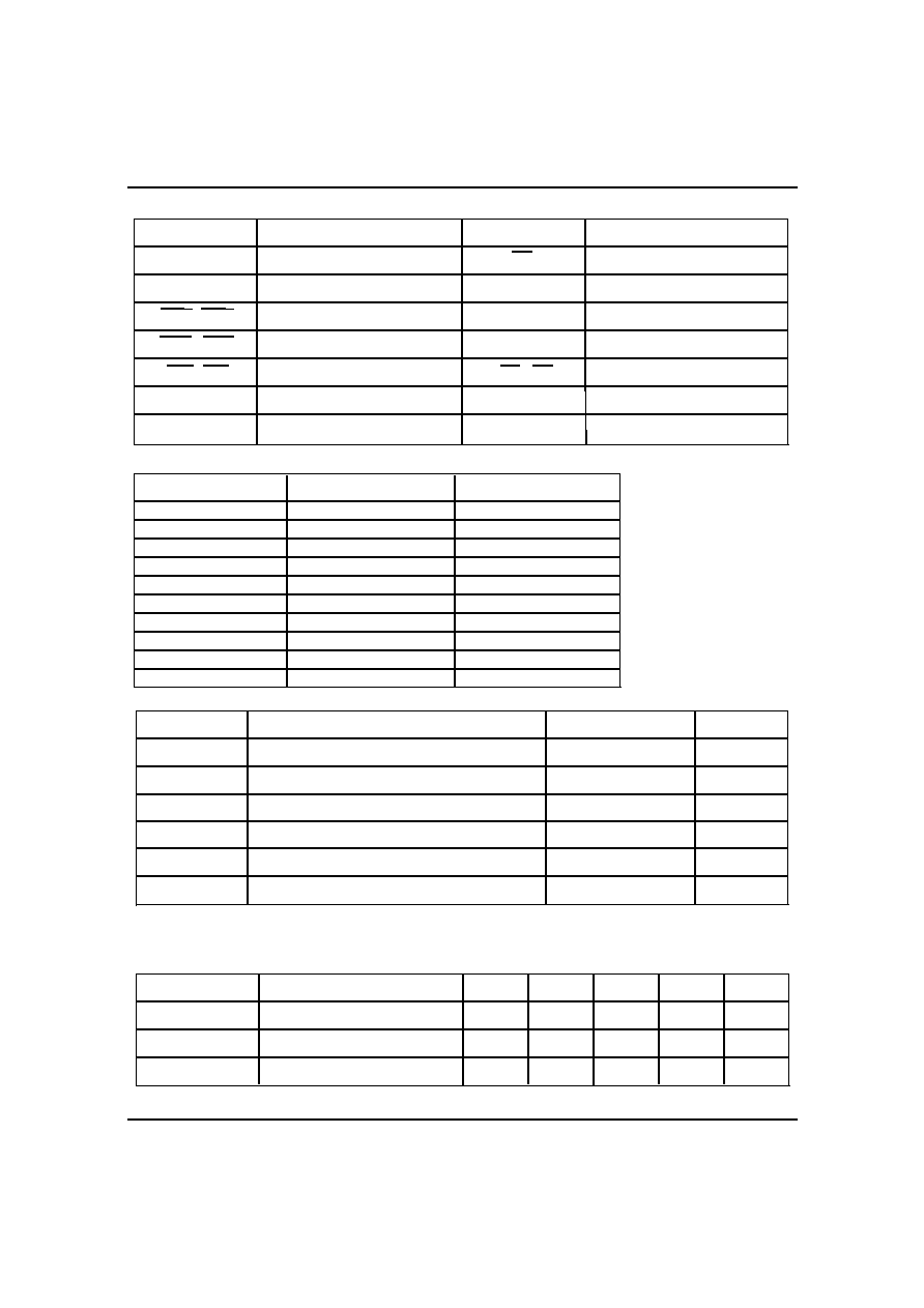
Absolute Maximum Ratings*
*
Note: 1. Stress greater than above Absolute Maximum Ratings may cause permanent damage to the device.
Recommended DC Operating Conditions (T
A
= 0 ~ 70C)
Symbol
Parameter
Unit
V
CC
V
IH
V
IL
Supply Voltage
Input High Voltage
Input Low Voltage
V
V
V
Max
3.6
Typ
3.3
-
-
Min
3.0
Note
1
1
1
Symbol
Parameter
Rating
Unit
T
A
T
STG
V
IN
/V
OUT
0 ~ 70
-55 ~ 125
-0.5 ~ 4.6
Ambient Temperature under Bias
Storage Temperature (Plastic)
Voltage on any Pin Relative to V
SS
V
I
OUT
50
Short Circuit Output Current
mA
P
D
12
Power Dissipation
W
C
C
2.0
-0.3
Vcc+0.3
0.8
*
Note: 1. All voltages referenced to V
SS
.
Pin Description
Pin
Function
Pin
Function
A0-A11, B0
DQ0-DQ71
V
CC
V
SS
NC
Address Inputs
Data Input/Output
Row Address Strobe
Column Address Strobe
Read/Write Enable
Power (+3.3V)
Ground
No Connection
RAS0, RAS2
CAS0, CAS4
WE0, WE2
PDE
Presence Detect Enable
PD 1- 8
Presence Detect
ID 0-1
ID bit
RSVD
Reserved Use
RFU
Reserved for Future Use
OE0, OE2
Output Enable
Presence Detect Pins (Optional)
Pin
50ns
60ns
PD1
PD2
1
PD3
PD4
1
1
0
1
1
0
1
PD5
PD6
1
0
1
1
0
PD7
PD8
0
0
1
0
ID0
ID1
0
0
0
Vcc
Voltage on Vcc Pin Relative to V
SS
-0.5 ~ 4.6
V
* 0 : Vss
1 : NC or Vcc
LG Semicon
GMM7738280CTG-5/6
4
DC Electrical Characteristics: (V
CC
= 3.3V+/-0.3V, T
A
= 0 ~ 70C)
Note: 1. I
CC
depends on output load condition when the device is selected. I
CC(max)
is specified at the
output open condition.
2. Address can be changed once or less while RAS = V
IL
.
3. Address can be changed once or less while CAS = V
IH
.
Unit
Note
V
V
uA
uA
§ Ì
§ Ì
§ Ì
§ Ì
§ Ì
§ Ì
§ Ì
1,2
1,3
2
1
Symbol
Parameter
V
OH
V
OL
Output Level
Output ``H`` Level Voltage (I
OUT
= -2§ Ì
)
Output Level
Output ``L`` Level Voltage (I
OUT
= 2§ Ì
)
I
CC1
Operating Current
Average Power Supply Operating Current
(RAS, CAS Cycling:
t
RC
=
t
RC
min)
I
CC2
Standby Current (TTL)
Power Supply Standby Current
(RAS, CAS = V
IH
, D
OUT
= High-Z)
I
CC3
RAS-Only Refresh Current
Average Power Supply Current
RAS-Only Refresh Mode
(RAS Cycling, CAS = V
IH
, t
RC
= t
RC
min)
I
CC4
Extended Data Out Mode Current
Average Power Supply Current
Extended Data Out Mode
(RAS = V
IL
, CAS, Address Cycling:
t
PC
=
t
PC
min
)
I
CC5
Standby Current (CMOS)
Power Supply Standby Current
(RAS, CAS>=V
CC
-0.2V, D
OUT
= High-Z)
I
CC6
CAS-before-RAS Refresh Current
(t
RC
= t
RC
min)
I
CC7
Standby Current
I
I(L)
I
O(L)
Input Leakage Current, Any Input
(0V V
IN
Vcc)
Output Leakage Current
(D
OUT
is Disabled, 0V V
OUT
Vcc)
RAS = V
IH
CAS = V
IL
D
OUT
= Enable
GMM7738280CTG
Min
Max
50ns
60ns
2.4
0
-
-
-
-
-
-
-
-
-
-
-
-5
-5
50ns
60ns
50ns
60ns
50ns
60ns
Vcc
0.4
1325
1235
1325
1235
1325
1235
38
1010
920
24.5
65
5
5
LG Semicon
GMM7738280CTG-5/6
5
Capacitance (V
CC
= 3.3V+/-0.3V, T
A
= 25C, f = 1MHz)
Symbol
Parameter
Note
Unit
Max
Min
C
I1
C
I2
C
13
Input Capacitance (A0~A12,B0)
Input Capacitance (WE0, WE2, OE0, OE2)
Input Capacitance (RAS0,RAS2)
1
1, 2
1, 2
pF
pF
pF
20
20
45
-
-
-
C
14
Input Capacitance (CAS0,CAS4)
1, 2
pF
20
-
C
I/O
I/O Capacitance (DQ0~DQ71)
1, 2
pF
20
-
Note: 1. Capacitance measured with Boonton Meter or effective capacitance measuring method.
2. CAS = V
IH
to disable D
OUT
.
Read, Write, Read-Modify-Write and Refresh Cycles (Common Parameters)
AC Characteristics (V
CC
= 3.3V+/-0.3V, T
A
= 0 ~ 70C, Notes 1, 2,19)
Test Conditions
Input rise and fall times : 2ns Output timing reference levels : V
OL
/V
OH
= 0.8/2.0V
Input level : V
IL
/V
IH
= 0.0/3.0V Output load : 1 TTL gate+C
L
(100pF)
Input timing reference levels : V
IL
/V
IH
= 0.8/2.0V (Including scope and jig)
Symbol
Max
Max
Min
t
RC
t
RP
t
RAS
t
CAS
t
ASR
t
RAH
t
ASC
t
CAH
t
RCD
4
t
RAD
3
t
RSH
t
CSH
t
CRP
Min
84
30
50
8
5
8
0
8
12
10
18
35
10
-
-
10000
-
-
-
-
32
20
-
-
-
Unit Notes
§ À
§ À
§ À
§ À
§ À
§ À
§ À
§ À
§ À
§ À
§ À
§ À
§ À
t
T
t
REF
Refresh Period ( 4096 Cycles)
2
-
50
64
§ À
ms
t
ODD
t
DZO
t
DZC
18
0
0
-
-
-
§ À
§ À
§ À
60
10
104
-
40
-
10000
5
-
10
-
0
-
10
-
14
40
12
25
20
-
40
-
10
-
20
-
0
-
0
-
2
50
-
64
t
CP
8
-
§ À
10
-
10000
10000
GMM7738280CTG-5
GMM7738280CTG-6
Parameter
Random Read or Write Cycle Time
RAS Precharge Time
RAS Pulse Width
CAS Pulse Width
Row Address Set-up Time
Row Address Hold Time
Column Address Set-up Time
Column Address Hold Time
RAS to CAS Delay Time
RAS to Column Address Delay Time
RAS Hold Time
CAS Hold Time
CAS to RAS Precharge Time
TransitionTime
(Rise and Fall)
OE to D
IN
Delay Time
OE Delay Time from D
IN
CAS Set-up Time from D
IN
CAS Precharge Time
5
6
6
7
LG Semicon
GMM7738280CTG-5/6
6
Read Cycles
Symbol
Max
Max
Min
Min
-
-
-
0
0
0
30
50
18
30
-
-
-
Unit
Notes
§ À
§ À
§ À
§ À
§ À
§ À
§ À
§ À
-
t
RAC
t
CAC
t
AA
t
RCS
t
RCH
t
RRH
t
RAL
t
CAL
8,9
t
OAC
-
18
-
20
§ À
-
60
-
20
-
35
0
-
0
-
0
-
35
-
18
-
15
-
9,10,17
§ À
§ À
t
RDD
t
WDD
§ À
t
OFR
§ À
t
WEZ
-
15
-
15
15
-
-
15
-
13
-
13
13
-
13
-
§ À
§ À
§ À
t
CLZ
t
OH
t
CDD
CAS to Output in Low - Z
18
-
§ À
§ À
t
OHR
t
OEZ
§ À
t
OFF
20
-
-
20
-
20
-
3
-
-
2
18
-
18
-
3
-
-
-
§ À
t
RCHR
60
-
50
-
§ À
t
OHO
3
-
3
-
2
9
3
3
GMM7738280CTG-5
GMM7738280CTG-6
Parameter
Access Time from RAS
Access Time from CAS
Access Time from Column Address
Read Command Set-up Time
Read Command Hold Time to CAS
Read Command Hold Time to RAS
Column Address to RAS Lead TIme
Column Address to CAS Lead Time
Access Time from OE
RAS to D
IN
Delay Time
Output Buffer Turn-off Delay Time from RAS
Output Buffer Turn-off Delay Time from WE
Output Data Hold Time
CAS to D
IN
Delay Time
Output Data Hold Time from RAS
Output Buffer Turn-off Delay Time from OE
WE to D
IN
Delay Time
Read Command Hold Time from RAS
Output Buffer Turn-off Delay Time from CAS
9,11,17
12
12
13,21
13
5
13
21
13,21
21
Output Data Hold Time from OE
LG Semicon
GMM7738280CTG-5/6
7
Wrtie Cycles
Read-Modify-Write Cycles
t
RWC
t
RWD
t
CWD
t
AWD
Refresh Cycle
Symbol
Max
Max
Min
Min
116
72
30
42
-
-
-
-
Unit Notes
§ À
§ À
§ À
§ À
Refresh Cycles
t
CSR
Symbol
CAS Set-up Time
(CAS-before-RAS Refresh Cycle)
t
CHR
CAS Hold Time
(CAS-before-RAS Refresh Cycle)
Parameter
Max
Max
Min
Min
5
-
Unit Notes
§ À
8
-
-
§ À
§ À
t
OEH
13
-
§ À
140
84
34
49
15
-
-
-
-
-
14
5
10
10
-
-
t
RPC
RAS Precharge to CAS Hold Time
5
-
§ À
5
-
-
t
WCS
t
WCH
t
WP
t
RWL
t
CWL
t
DS
t
DH
Symbol
Write Command Set-up Time
Write Command Hold Time
Write Command Pulse Width
Write Command to RAS Lead Time
Write Command to CAS Lead Time
Data-in Set-up Time
Data-in Hold Time
Parameter
Max
Max
Min
Min
0
8
8
8
0
13
-
-
-
-
-
-
Unit Notes
§ À
§ À
§ À
§ À
§ À
§ À
§ À
-
14
15
15
0
10
10
10
0
15
-
-
-
-
-
-
-
Read-Modify-Write Cycle Time
RAS to WE Delay Time
CAS to WE Delay Time
Column Address to WE Delay Time
Parameter
OE Hold Time from WE
18
20
14
14
GMM7738280CTG-5
GMM7738280CTG-6
GMM7738280CTG-5
GMM7738280CTG-6
GMM7738280CTG-5
GMM7738280CTG-6
21
t
WRP
WE setup Time
(CAS-before-RAS Refresh Cycle)
t
WRH
WE Hold Time
(CAS-before-RAS Refresh Cycle)
5
8
5
§ À
LG Semicon
GMM7738280CTG-5/6
8
Present Detect Read cycle
Symbol
Max
Max
Min
Min
Unit
Notes
ns
§ À
GMM7738280CTG-5
GMM7738280CTG-6
t
PD
t
PDOFF
Parameter
PDE to Valid PD bit
PDE to PD bit in active
10
10
7
7
2
2
-
-
28
§ À
§ À
-
-
35
33
-
100000
§ À
40
-
100000
t
RASP
t
ACP
t
RHCP
28
-
§ À
35
-
8
5
-
-
§ À
§ À
10
5
-
-
5
-
§ À
§ À
5
-
8
-
10
-
t
COL
t
COP
t
OEP
t
RCHP
EDO Mode RAS Pulse Width
Access Time from CAS Precharge
RAS Hold Time from CAS Precharge
OE Precharge Time
CAS Hold Time Referred OE
CAS to OE set-up Time
Read Command Hold Time from CAS
Precharge
Output Data Hold Time from CAS Low
16
Max
Max
Min
Min
20
8
-
-
Unit
Notes
§ À
§ À
25
10
-
-
Extended Data Out Mode Cycles
t
HPC
t
WPE
Symbol
EDO Page Mode Cycle Time
Write pulse width during CAS Precharge
Parameter
GMM7738280CTG-5
GMM7738280CTG-6
t
DOH
Max
Max
Min
Min
57
45
-
-
Unit
Notes
§ À
§ À
68
54
-
-
EDO Page Mode Read-Modify-Write cycle
t
HPRWC
t
CPW
Symbol
EDO Page Mode Read-Modify-Write Cycle Time
WE delay time from CAS precharge
Parameter
20
9,17
9,22
14
GMM7738280CTG-5
GMM7738280CTG-6

LG Semicon
GMM7738280CTG-5/6
9
Notes:
AC measurements assume t
T
= 2§ À
.
AC initial pause of 200
us is required after power up followed by a minimum of eight
initialization cycles ( any combination of cycles containing RAS-only refresh or CAS-before-
RAS refresh)
Operation with the t
RCD
(max) limit insures that t
RAC
(max) can be met, t
RCD
(max) is specified as a
reference point only: if t
RCD
is greater than the specified t
RCD
(max) limit, then access time is
controlled exclusively by t
CAC
.
Operation with the t
RAD
(max) limit insures that t
RAC
(max) can be met, t
RAD
(max) is specified as a
reference point only: if t
RAD
is greater than the specified t
RAD
(max) limit, then access time is
controlled exclusively by t
AA
.
Either t
OED
or t
CDD
must be satisfied.
Either t
DZO
or t
DZC
must be satisfied.
V
IH
(min) and V
IL
(max) are reference levels for measuring timing of input signals. Also,
transition times are measured between V
IH
(min) and V
IL
(max).
Assumes that t
RCD
<=t
RCD
(max) and t
RAD
<=t
RAD
(max). If t
RCD
or t
RAD
is greater than the maximum
recommended value shown in this table, t
RAC
exceeds the value shown.
Measured with a load circuit equivalent to 1 TTL loads and 100 pF.
Assumes that t
RCD
>=t
RCD
(max) and t
RCD
+
t
CAC
(max) >=t
RAD
+
t
AA
(max).
Assumes that t
RAD
>=t
RAD
(max) and t
RCD
+
t
CAC
(max)
<=t
RAD
+
t
AA
(max).
Either t
RCH
or t
RRH
must be satisfied for a read cycles.
t
OFF
(max),
t
OEZ(
max), t
OFR
(max) and t
WEZ
(max) define the time at which the outputs achieve the
open circuit condition and is not referenced to output voltage levels.
t
WCS
, t
RWD
, t
CWD,
t
AWD,
and t
CPW
are not restrictive operating parameters. They are included in the
data sheet as electrical characteristics only: if t
WCS
>=t
WCS
(min), the cycle is an early write cycle
and the data out pin will remain open circuit (high impedance) throughout the entire cycle: if
t
RWD
>=t
RWD
(min), t
CWD
>=t
CWD
(min), t
AWD
>=t
AWD
(min) and t
CPW
>=t
CPW
(min), the cycle is a read-
modify-write and the data output will contain data read from the selected cell: if neither of the
above sets of conditions is satisfied, the condition of the data out (at access time) is
indeterminate.
t
DS
and t
DH
are referred to CAS leading edge in early write cycles and to WE leading edge in
delayed write or read-modify-write cycles.
t
RASP
defines RAS pulse width in extended data out mode cycles.
Access time is determined by the longest among t
AA,
t
CAC
and t
CPA
.
In delayed write or read-modify-write cycles, OE must disable output buffer prior to applying
data to the device.
When output buffers are enabled once, sustain the low impedance state until valid data is
obtained. When output buffer is turned on and off within a very short time, generally it causes
large V
CC
/V
SS
line noise, which causes to degrade V
IH
min/V
IL
max level.
1.
2.
3.
4.
5.
6.
7.
8.
9.
10.
11.
12.
13.
14.
15.
16.
17.
18.
19.

LG Semicon
GMM7738280CTG-5/6
10
t
HPC
(min) can be achieved during a series of EDO mode early write cycles or EDO mode read
cycles. If both write and read operation are mixed in a EDO mode, RAS cycle { EDO mode mix
cycle (1),(2) } minimum value of CAS cycle t
HPC
(t
CAS
+ t
CP
+ 2t
T
) becomes greater than the
specified t
HPC
(min) value.
Data output turns off and becomes high impedance from later rising edge of RAS and CAS.
Hold time and turn off time are specified by the timing specifications of later rising edge of RAS
and CAS between t
OHR
and t
OH
, and between t
OFR
and t
OFF
.
t
DOH
defines the time at which the output level go cross. V
OL
=0.8V, V
OH
=2.0V of output timing
reference level.
Before and after self refresh mode, execute CBR refresh to all refresh addresses in or within 64
§ Â
period on the condition a and b below.
a. Enter self refresh mode within 15.6 us after either burst refresh or distributed refresh at equal
interval to all refresh addresses are completed.
b. Start burst refresh or distributed refresh at equal interval to all refresh addressed within 15.6us
after exiting from self refresh mode.
In case of entering from RAS-only-refresh, it is necessary to execute CBR refresh before and
after self refresh mode according as note 23.
For L_version, it is available to apply each 128
§ Â
and 31.2 us instead of 64 § Â
and 15.6us at
note 23.
At t
RASS
£ ¾
100 us , self refresh mode is activated, and not activated at t
RASS
£ ¼
10us. It is undefined
within the range of 10 us £ ¼
t
RASS
£ ¼
100 us . for t
RASS
£ ¾
10 us , it is necessary to satisfy t
RPS
.
XXX: H or L ( H : V
IH
(min)<=V
IN
<=V
IH
(max), L: V
IH
(min)<=V
IN
<=V
IH
(max))
///////: Invalid Dout
When the address, clock and input pins are not described on timing waveforms, their pins must
be applied V
IH
or V
IL.
20.
21.
22.
23.
24.
25.
26.
27.
The value of CAS cycle time of mixed EDO page mode is shown in
EDO page mode mix cycle (1) and (2).
LG Semicon
GMM7738280CTG-5/6
11
Timing Waveforms
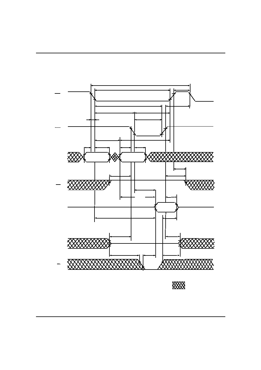
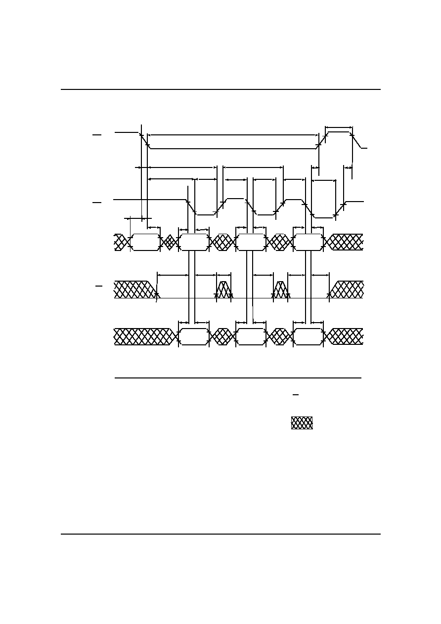
FIGURE 1. READ CYCLE
*
: Don`t care
t
RC
t
RAS
t
RP
RAS
t
CSH
t
CRP
t
RCD
t
RSH
t
CAS
t
T
t
RAD
t
RAL
t
ASR
t
RAH
ADDRESS
ROW
COLUMN
t
RCS
t
RCH
t
RRH
WE
t
ASC
t
CAH
D
OUT
D
OUT
D
IN
t
DZC
t
CDD
High-Z
t
OED
OE
t
DZO
t
OAC
t
CAC
t
AA
High-Z
t
RAC
t
OEZ
t
OFF
CAS
LG Semicon
GMM7738280CTG-5/6
12
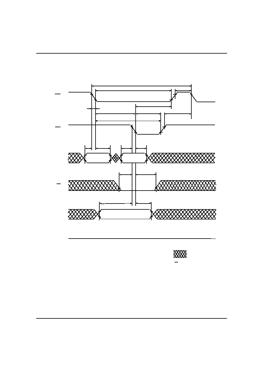
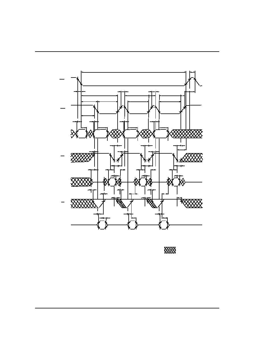
FIGURE 2. EARLY WRITE CYCLE
t
WCS
t
WCH
*
: Don`t care
WE
D
OUT
**
OE : Don`t care
D
IN
t
DS
t
DH
High-Z
t
RC
t
RAS
t
RP
RAS
t
CSH
t
CRP
t
RCD
t
RSH
t
CAS
t
T
CAS
t
ASR
t
RAH
t
ASC
t
CAH
ADDRESS
COLUMN
ROW
***
t
WCS
t
WCS
(min)
>
=
D
IN
LG Semicon
GMM7738280CTG-5/6
13
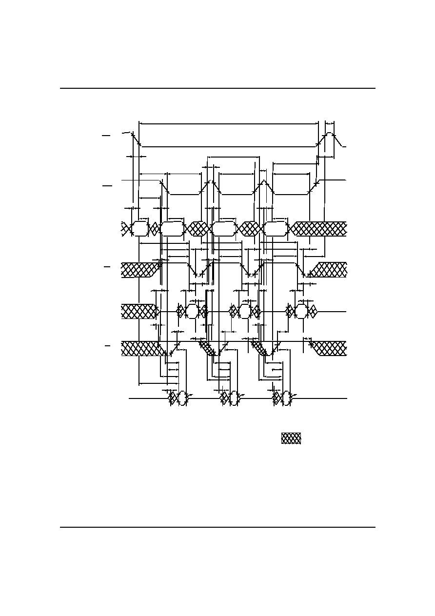
FIGURE 3. DELAYED WRITE CYCLE
t
RC
t
RAS
t
RP
RAS
t
CSH
t
CRP
t
RCD
t
RSH
t
CAS
t
T
CAS
t
ASR
t
RAH
t
ASC
t
CAH
ADDRESS
COLUMN
t
RCS
*
: Don`t care
WE
D
OUT
ROW
D
IN
t
WP
t
RWL
t
CWL
t
OED
t
OEH
INVALID
OUTPUT
D
IN
OE
**
Invalid D
OUT
comes out,
when OE is low level.
t
DZC
t
DH
t
DS
High-Z
t
DZO
t
OEZ
**
High-Z
LG Semicon
GMM7738280CTG-5/6
14
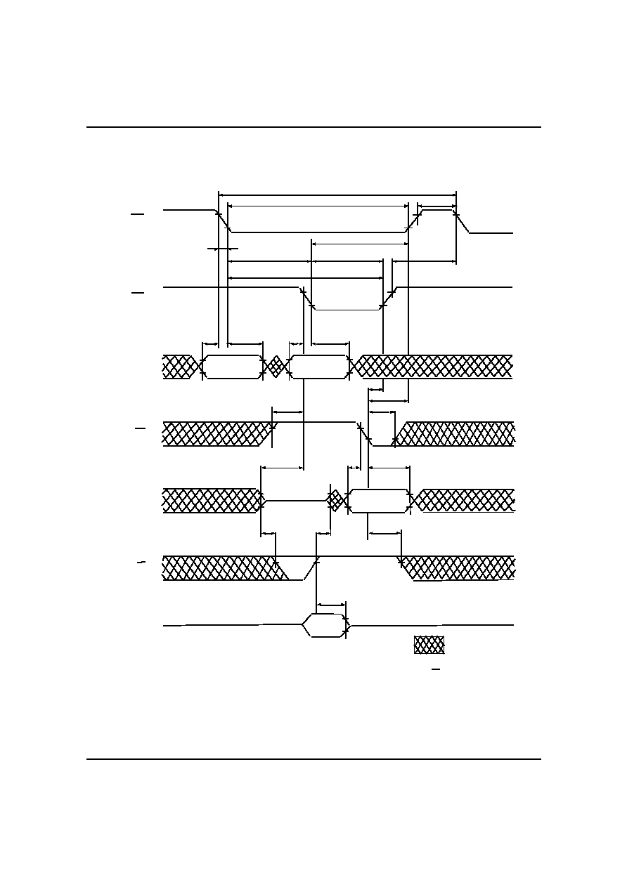
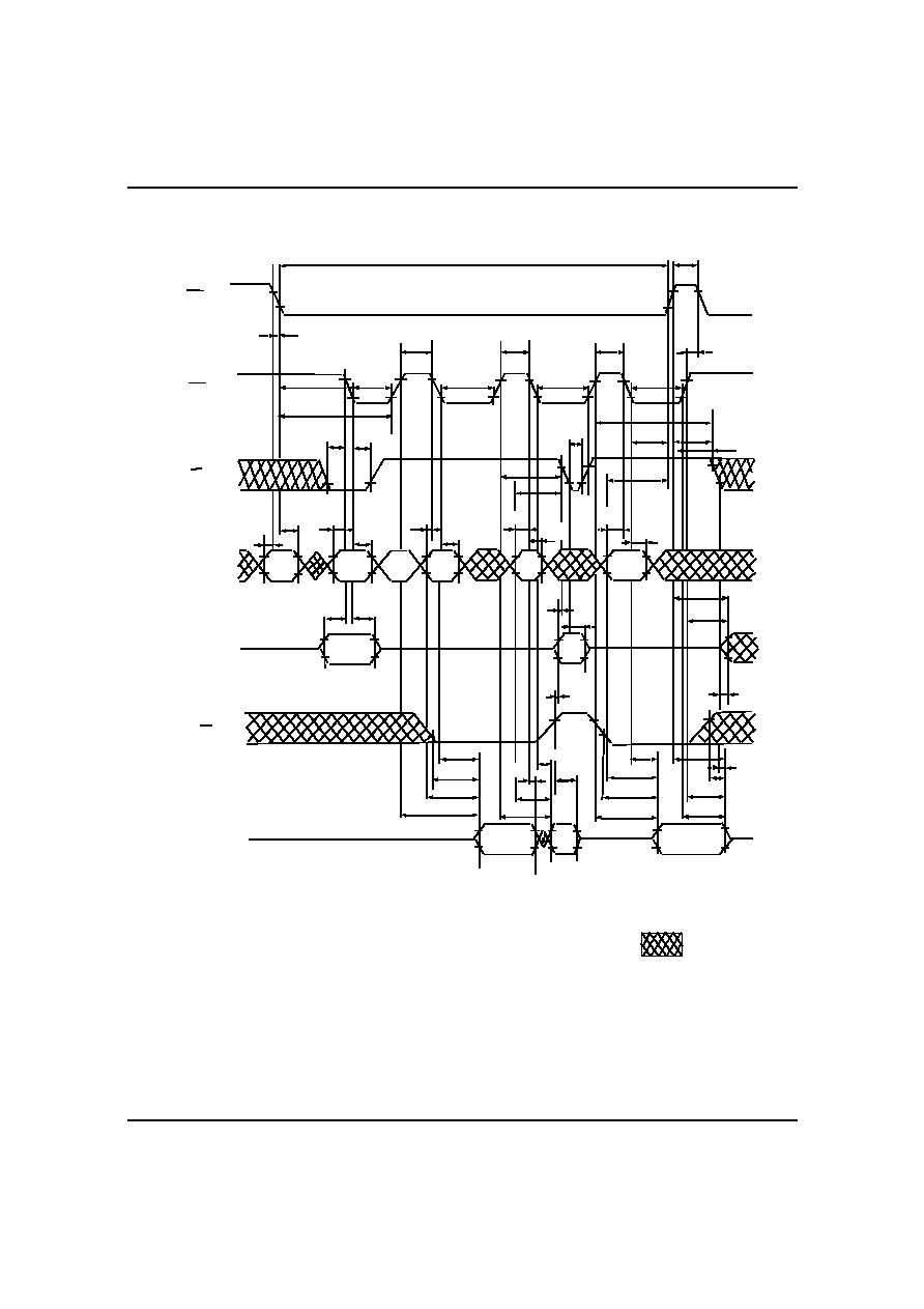
FIGURE 4. READ MODIFY WRITE CYCLE
t
RWC
t
RAS
t
RP
RAS
t
CRP
t
RCD
t
T
t
ASR
t
RAH
t
ASC
t
CAH
ADDRESS
COLUMN
*
: Don`t care
WE
ROW
D
IN
t
WP
t
RWL
t
CWL
t
OED
t
OEH
D
IN
t
DZC
t
DH
t
DS
High-Z
t
RAD
t
CWD
t
AWD
t
RWD
t
RCS
t
DZO
D
OUT
D
OUT
t
OAC
OE
t
OEZ
t
CAC
t
AA
t
RAC
CAS
t
CAS
High-Z
LG Semicon
GMM7738280CTG-5/6
15
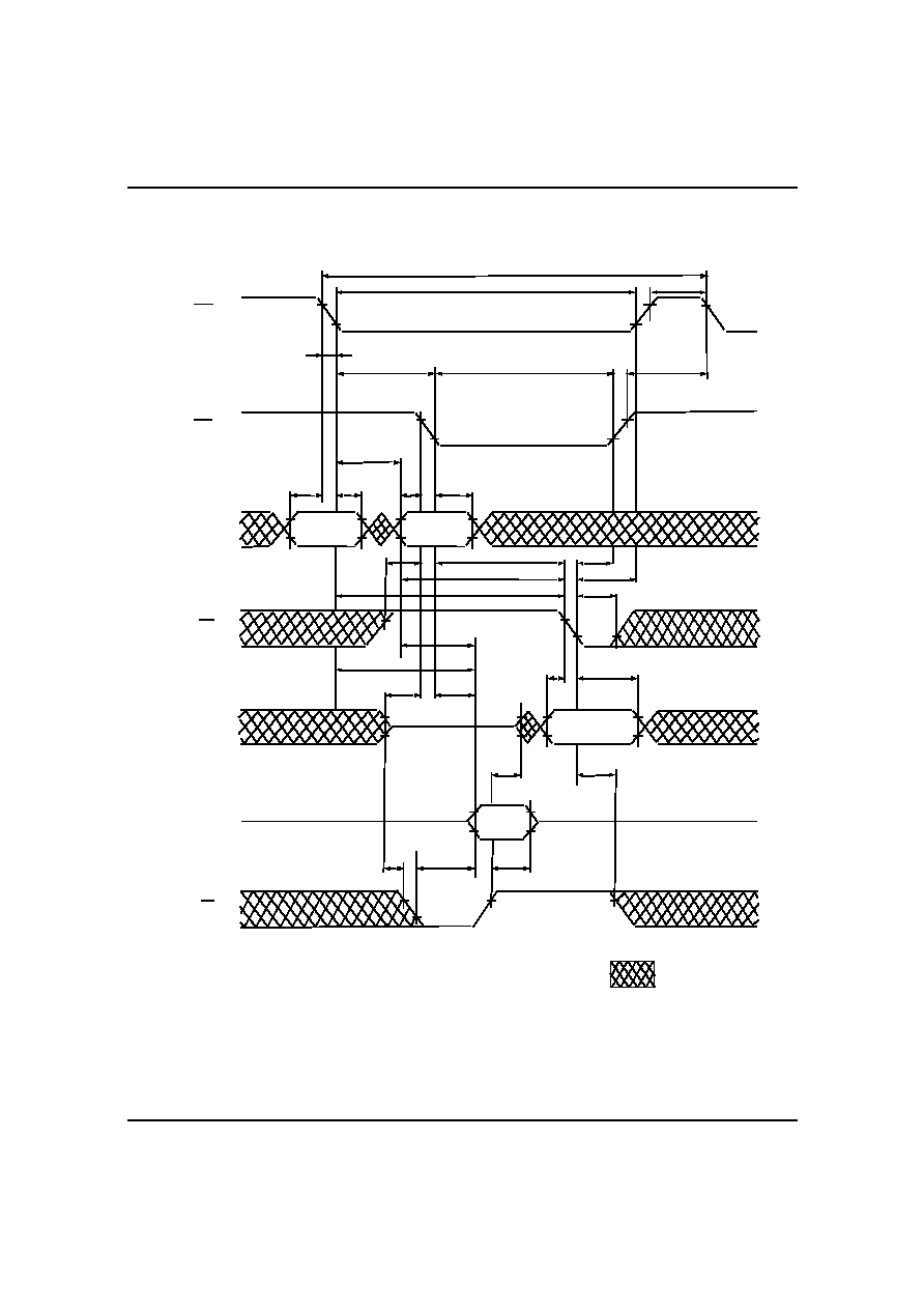
FIGURE 5. RAS ONLY REFRESH CYCLE
RAS
CAS
ADDRESS
ROW
D
OUT
High-Z
t
ASR
t
RAH
t
CRP
t
RPC
t
RP
t
RAS
t
RC
t
T
FIGURE 6. CAS BEFORE RAS REFRESH CYCLE
t
CRP
RAS
t
RP
t
T
CAS
D
OUT
High-Z
t
OFF
t
RAS
t
RP
t
RAS
t
RP
t
RC
t
RC
t
CPN
t
RPC
t
CSR
t
CHR
t
CPN
t
RPC
t
CSR
t
CHR
t
CRP
ADDRESS
*
**
WE : V
IH
: Don`t care
*
OE,WE : Don`t care
**
Rrfresh address :
A0~A12 (AX0 ~ AX12)
INVALID
D
OUT
LG Semicon
GMM7738280CTG-5/6
16
FIGURE 7. HIDDEN REFRESH CYCLE
RAS
t
RAS
t
T
*
: Don`t care
t
RC
t
RC
ADDRESS
WE
t
RP
t
RAS
t
RP
t
RAS
t
RP
t
RC
t
RCD
t
RSH
t
CHR
t
CRP
t
RAD
t
RAL
COLUMN
ROW
t
ASR
t
RAH
t
ASC
t
CAH
t
RCS
D
OUT
D
OUT
OE
D
IN
High-Z
t
CAS
t
RRH
t
RCH
t
DZC
t
CAC
t
AA
t
RAC
t
DZO
t
OAC
t
OED
t
CDD
t
OEZ
t
OFF
CAS
(Refresh)
(Refresh)
(Read)
High-Z
LG Semicon
GMM7738280CTG-5/6
17
FIGURE 8. EXTENDED DATA OUT MODE READ CYCLE
CAS
RAS
ADDRESS
WE
t
RASP
t
RP
t
RHCP
*
: Don`t care
ROW
COLUMN
COLUMN
COLUMNN
OE
t
T
t
RCD
t
CAS
t
CAS
t
HPC
t
RSH
t
CP
t
ASR
t
RAH
t
RAD
t
ASC
t
ASC
t
CAH
t
RCS
t
RCH
t
RAL
D
OUT
D
OUT
1
D
OUT
2
D
OUT
N
t
RAC
t
AA
t
RRH
t
WEZ
t
OFR
t
OFF
t
CPA
t
AA
t
CAC
t
CPA
t
AA
t
CAC
t
CAC
t
DOH
t
DOH
t
OEZ
t
OAC
t
ASC
t
CAH
t
CAS
t
CP
High-Z
t
RCHC
t
RCHA
t
OHR
t
OH
t
CSH
t
CRP
t
CSH
t
CAH
LG Semicon
GMM7738280CTG-5/6
18
RAS
ADDRESS
WE
OE
D
OUT
CAS
ROW
COLUMN 1
COLUMN 2
COLUMN N
D
OUT
1
D
OUT
2
High-Z
D
OUT
3
D
OUT
N
D
OUT
2
t
T
t
CAS
t
CSH
t
CP
t
HPC
t
RAC
t
AA
t
CAC
t
OAC
t
ASR
t
RAH
t
CAH
t
CP
t
CAS
t
CAS
t
HPC
t
CP
t
CAS
t
RSH
t
CPRH
t
HPC
t
RP
t
RASP
t
CRP
t
RCH
t
RCS
t
RCHR
t
CAL
t
ASC
t
CAH
t
ASC
t
CAH
t
ASC
t
CAH
t
RAL
t
CAL
t
CAL
t
CAL
t
COL
t
COP
t
AA
t
CAC
t
WEZ
t
OEZ
t
OAC
t
AA
t
CAC
t
DOH
t
OEZ
t
OAC
t
CAC
t
AA
t
CPA
t
OFR
t
OHR
t
OEZ
t
OFF
t
OH
COLUMN 3
t
RCH
t
RCS
t
ASC
t
RCHC
t
RRH
t
CPA
t
CPA
FIGURE 9. EXTENDED DATA OUT MODE READ CYCLE (OE CONTROL)*
*NOTE : EDO Hi-Z control by OE or WE. OE rising edge disables data outputs. When OE goes high
during CAS high, the data will not come out until next CAS access. When WE goes low during
CAS high, the data will not come out until next CAS access.
LG Semicon
GMM7738280CTG-5/6
19
FIGURE 10. EXTENDED DATA OUT MODE EARLY WRITE CYCLE
RAS
D
IN
ADDRESS
WE
t
T
COLUMN 1
ROW
COLUMN 2
COLUMN N
t
RCD
t
CAS
t
CSH
t
CP
t
CAS
t
HPC
t
CP
t
CAS
t
ASR
t
RAH
t
RASP
t
RP
D
IN
1
D
IN
2
D
IN
N
D
OUT
High-Z
t
RSH
t
CRP
t
ASC
t
CAH
t
ASC
t
CAH
t
ASC
t
CAH
t
WCS
t
WCH
t
WCS
t
WCH
t
WCS
t
WCH
t
DS
t
DH
t
DS
t
DH
t
DS
t
DH
***
: Don`t care
OE : Don`t care
CAS
t
WCS
>=t
WCS
(min)
**
*
LG Semicon
GMM7738280CTG-5/6
20
FIGURE 11. EXTENDED DATA OUT MODE DELAYED WRITE CYCLE
CAS
RAS
*
: Don`t care
D
IN
ADDRESS
WE
ROW
D
OUT
INVALID
D
OUT
>
** t
OEH
t
CWL
=
OE
COLUMN 1
D
IN
1
COLUMN 2
COLUMN N
t
RASP
t
RP
t
T
t
RCD
t
CAS
t
CSH
t
CP
t
CAS
t
HPC
t
CP
t
CAS
t
RSH
t
CRP
t
ASR
t
RAD
t
RAH
t
ASC
t
CAH
t
ASC
t
CAH
t
RCS
t
RCS
t
CWL
t
CWL
t
RCS
t
CWL
t
RWL
t
DZC
t
WP
t
DS
t
DH
t
DZC
t
WP
t
DS
t
DH
t
DZC
t
WP
t
DS
t
DH
t
ASC
t
CAH
t
DZO
t
OED
t
OEH
t
DZO
D
IN
2
t
OED
t
DZO
t
OEH
D
IN
N
t
OED
t
OEH
t
CLZ
t
OEZ
INVALID
D
OUT
t
CLZ
t
OEZ
INVALID
D
OUT
t
OEZ
t
CLZ
High-Z
LG Semicon
GMM7738280CTG-5/6
21
FIGURE 12. EXTENDED DATA OUT MODE READ MODIFY WRITE CYCLE
*
: Don`t care
** t
OEH
t
CWL
>
=
RAS
D
IN
ADDRESS
WE
ROW
D
OUT
OE
COLUMN 1
D
IN
1
COLUMN 2
COLUMN N
t
RASP
t
RP
t
T
t
RCD
t
CAS
t
CP
t
CAS
t
HPRWC
t
CP
t
CAS
t
RSH
t
CRP
t
ASR
t
RAD
t
RAH
t
ASC
t
CAH
t
ASC
t
CAH
t
RCS
t
RCS
t
CWL
t
CWL
t
RCS
t
CWL
t
RWL
t
DZC
t
WP
t
DS
t
DH
t
DZC
t
WP
t
DS
t
DH
t
WP
t
DS
t
DH
t
ASC
t
CAH
t
OED
t
OEH
D
IN
2
t
OED
t
OEH
D
IN
N
t
OED
t
OEH
t
RWD
t
AWD
t
CWD
t
CPW
t
AWD
t
CWD
t
CPW
t
AWD
t
CWD
t
DZC
t
DZO
t
DZO
t
OAC
t
CAC
t
AA
t
RAC
t
CLZ
t
OEZ
D
OUT
1
D
OUT
2
D
OUT
N
High-Z
t
OAC
t
CAC
t
CPA
t
CLZ
t
OEZ
t
AA
t
OAC
t
CPA
t
CLZ
t
OEZ
t
AA
t
CAC
t
DZO
CAS
High-Z
LG Semicon
GMM7738280CTG-5/6
22
FIGURE 13. EXTENDED DATA OUT MODE MIX CYCLE (1)
*23
RAS
t
RASP
t
RP
t
T
t
CP
t
CP
t
CAS
t
CAS
t
CP
t
CAS
t
CRP
t
RCD
t
CSH
t
CAS
ADDRESS
ROW
COLUMN
1
COLUMN
2
COLUMN
3
COLUMN
4
OE
D
IN
1
D
IN
3
Dout
D
OUT
2
D
OUT
4
t
RAH
t
ASR
t
CAH
t
CAH
t
CAH
t
CAH
High - Z
t
RDD
t
CDD
t
DS
t
DH
t
OED
t
DOH
t
CAC
t
CAC
t
CAC
t
WEZ
*
Din
t
ASC
t
ASC
t
ASC
t
ASC
t
WCS
t
WCH
t
DS
t
DH
t
WDD
t
AA
t
OAC
t
CPA
t
CPA
t
AA
t
OEZ
t
OEZ
t
AA
t
OAC
t
CPA
t
OH
D
OUT
3
: Don`t care
t
OFF
t
OFR
t
CPW
t
AWD
t
WP
t
RCHC
t
RSH
t
RRH
t
RCH
t
RAL
CAS
WE
High - Z
LG Semicon
GMM7738280CTG-5/6
23
FIGURE 14. EXTENDED DATA OUT MODE MIX CYCLE (2)
*23
RAS
t
RASP
t
RP
t
T
WE
ADDRESS
ROW
COLUMN
1
COLUMN
2
COLUMN
3
COLUMN
4
OE
D
IN
2
D
IN
3
Dout
D
OUT
1
D
OUT
4
t
CSH
t
CP
t
CP
t
CAS
t
CAS
t
CP
t
CAS
t
CRP
t
RCD
t
RCHR
t
CAS
t
RCS
t
RCH
t
WCS
t
WCH
t
WP
t
RSH
t
RRH
t
RCH
t
RAH
t
ASR
t
ASC
t
CAH
t
ASC
t
ASC
t
CAH
t
CAH
t
CPW
t
RAL
t
ASC
t
CAH
High - Z
t
CAL
t
CAL
t
CAL
t
CAL
t
RDD
t
CDD
t
DS
t
DH
t
DS
t
DH
t
OED
t
COL
t
OED
t
COP
t
AA
t
CAC
t
OAC
t
CPA
t
CAC
t
OAC
t
CPA
t
AA
t
OEZ
t
OEZ
t
CAC
t
AA
t
OAC
t
RAC
t
WEZ
t
OEZ
t
OFF
t
OH
t
OFR
*
: Don`t care
Din
D
OUT
3
CAS
High - Z
LG Semicon
GMM7738280CTG-5/6
24
RAS
CAS
FIGURE 16. TEST MODE SET CYCLE
WE
FIGURE 15. TEST MODE CYCLE
**
: Don`t care
*
CBR or RAS-only refresh
***
Address, D
IN
, OE: Don`t care
Set Cycle***
Test Mode Cycle
Reset Cycle*
Normal Mode
~ ~
~ ~
~ ~
~ ~
*
: Don`t care
RAS
CAS
WE
ADDRESS
D
OUT
t
OFF
High-Z
t
WS
t
WH
t
CPN
t
RPC
t
CSR
t
CHR
t
RPC
t
CRP
t
CPN
t
RP
t
RAS
t
RP
t
RC
t
T
INVALID D
OUT
LG Semicon
GMM7738280CTG-5/6
25
FIGURE 16. CAS BEFORE RAS REFRESH COUNTER CHECK CYCLE (READ)
RAS
t
T
CAS
ADDRESS
*
: Don`t care
WE
DOUT
DIN
t
RC
t
RAS
t
RP
t
CAC
t
OEP
D
OUT
t
AA
t
RAC
COLUMN
t
CSR
t
CHR
t
CPT
t
RSH
t
CAS
t
CRP
t
ASC
t
CAH
t
WS
t
WH
t
RCH
t
RRH
OE
t
CDD
t
DZC
t
DZO
t
OEZ
t
OFF
t
OAC
High-Z
t
RCS
High-Z
t
OED
LG Semicon
GMM7738280CTG-5/6
26
RAS
t
T
CAS
ADDRESS
*
: Don`t care
WE
DOUT
DIN
t
RC
t
RAS
t
RP
COLUMN
t
CSR
t
CHR
t
CPT
t
RSH
t
CAS
t
CRP
t
ASC
t
CAH
t
WS
t
WH
t
WCS
High-Z
D
IN
t
WCH
t
DS
t
DH
OE
FIGURE 17. CAS BEFORE RAS REFRESH COUNTER CHECK CYCLE (WRITE)
LG Semicon
GMM7738280CTG-5/6
27
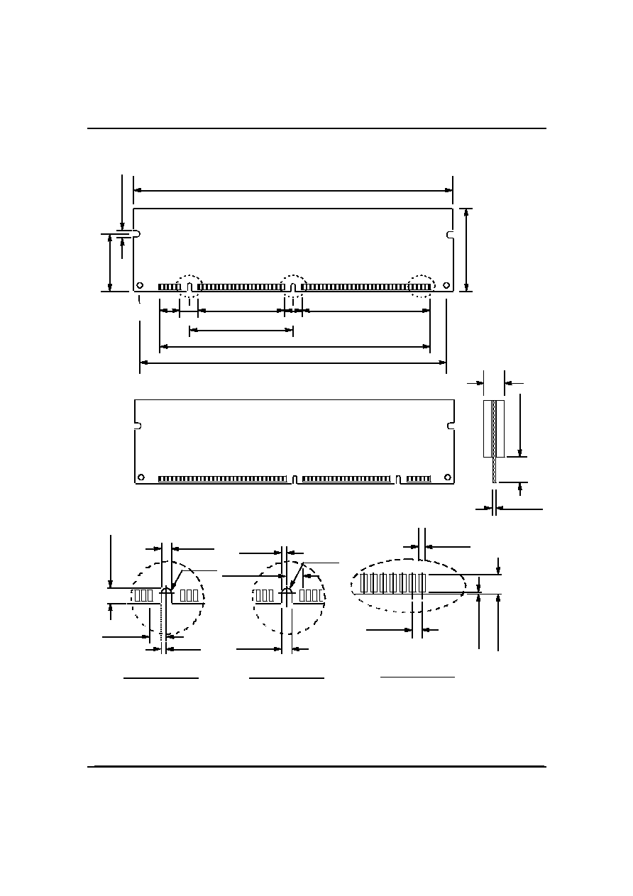
Package Dimension
85
168
1
84
5250(133.35)
5013.78(127.35)
1700(43.18)
1450(36.83)
2150(54.61)
450(11.43)
250(6.35)
700(17.78)
157.48(4.0)
1000(25.4)
"C"
"B"
"A"
4550(115.57)
Unit: mil (mm)
* (1 mil = 1/1000 inches)
NOTE : 1. Tolerances on all dimensions +/-5 (0.127) unless otherwise specified.
2. Thickness includes Plating and / or Metallization.
DETAIL "B"
DETAIL "A"
5.9(0.15)
100(2.54)
min.
39.37(1.0)
50(1.27)
78.74(2.0)
39.37(1.0)
DETAIL "C"
78.74(2.0)
122.83(3.12)
39.37(1.0)
125(3.175)
125(3.175)
R78.74
(2.0)
R78.74
(2.0)
157.48(4.0) max.
50(1.27)
157.48(4.0)
min.
(Front Side)
(Rear Side)