INTRO.PDF

4-BIT SINGLE CHIP MICROCOMPUTERS
GMS34XXXT SERIES
USER`S MANUAL
· GMS34004T
· GMS34112T
· GMS34140T

Revision 1.1
Published by MCU Application Team in HYNIX Semiconductor Inc.
All Right Reserved.
Editor's E-Mail :
rhja@hynix.com
Additional information of this manual may be served by HYNIX Semiconductor Inc.Offices in
Korea or Distributors and Representative listed at address directory.
HYNIX Semiconductor Inc.reserves the right to make changes to any Information here at any
time without notice.
The information, diagrams, and other data in this manual are correct and reliable; however, HYNIX
Semiconductor Inc.is in no way responsible for any violations of patents or other rights of the third
party generated by the use of this manual.

Table of Contents
Chapter 1
Introduction
Outline of Characteristics
Characteristics
Block Diagram
Pin Assignment and Terminal
Pin Dimension
Pin Description and Circuit
I/O circuit types and options
Electrical Characteristics
Chapter 2
Architecture
Block Description
Program Memory (ROM)
EPROM Address Register
Data Memory (RAM)
X-Register (X)
Y-Register (Y)
Accumulator (Acc)
Arithmetic and Logic Unit (ALU)
State Counter (SC)
Clock Generator
Pulse Generator
Initial Reset Circuit
Watch Dog Timer (WDT)
Stop Function
Port Operation
Chapter 3
Instruction
Table of Contents
............................................................................................1-1
.................................................................1-1
..................................................................................1-1
..................................................................................1-2
..........................................................1-3
..................................................................................1-4
.................................................................1-7
.............................................................1-8
................................................................1-10
...........................................................................................2-1
.............................................................................2-1
..................................................................2-1
................................................................2-2
........................................................................2-3
...................................................................................2-3
...................................................................................2-4
............................................................................2-4
.......................................................2-4
...........................................................................2-5
...............................................................................2-6
...............................................................................2-7
............................................................................2-8
.................................................................2-8
....................................................................................2-9
..................................................................................2-9
........................................................................................3-1

Table of Contents
Chapter 4
EPROM
GMS34004TK/34112TK/34140TK
Mode Define
Port Define
Programming Data
Write/Read Data Conversion
Checksum
Programming Control
Programming DC Specification
EPROM read mode(1/2)
EPROM read mode (2/2)
EPROM write mode (1/2)
EPROM write mode (2/2)
Lock bit write mode (1/2)
Lock bit write mode (2/2)
Lock bit read mode (1/2)
Lock bit read mode (2/2)
GMS34004T/112T/140T (Pin assignment & Package)
EPROM (KHz) mode
EPROM write only mode
GMS34004TK/34112TK/34140TK
Mode Define
Port Define
Programming Data
Write/Read Data Conversion
Checksum
Programming Control
Programming DC Specification
EPROM read mode(1/2)
EPROM read mode (2/2)
EPROM write mode (1/4)
EPROM write mode (2/4)
EPROM write mode (3/4)
EPROM write mode (4/4)
Lock bit write mode (1/3)
Lock bit write mode (2/3)
Lock bit write mode (3/3)
Lock bit read mode (1/2)
Lock bit read mode (2/2)
.................................................................................................4-1
.........................................................4-1
.....................................................................................4-1
.......................................................................................4-2
...........................................................................4-2
............................................................4-3
.........................................................................................4-3
........................................................................4-3
.........................................................4-3
...................................................................4-4
..................................................................4-4
..................................................................4-5
..................................................................4-5
..................................................................4-6
..................................................................4-6
..................................................................4-7
..................................................................4-7
.....................4-8
.........................................................................4-9
..................................................................4-9
.............................................................4-10
.....................................................................................4-10
........................................................................................4-11
...........................................................................4-11
............................................................4-12
........................................................................................4-12
......................................................................4-12
........................................................4-12
...................................................................4-13
...................................................................4-13
..................................................................4-14
..................................................................4-14
..................................................................4-15
..................................................................4-15
..................................................................4-16
..................................................................4-16
..................................................................4-16
..................................................................4-18
..................................................................4-18
INTRODUCTION
1
ARCHITECTURE
2
INSTRUCTION
3
EPROM
4
1 - 1
CHAPTER 1. Introduction
OUTLINE OF CHARACTERISTICS
The GMS340 series are remote control transmitter which uses CMOS technology,
and the EPROM version of GMS34XXX series.
This enables transmission code outputs of different configurations, multiple custom
code output, and double push key output for easy fabrication.
The GMS340 series are suitable for remote control of TV, VCR, FANS, Air-
conditioners, Audio Equipments, Toys, Games etc.
Characteristics
·
Program memory : 512bytes for GMS34004T
1,024 bytes for GMS34112T/140T
·
Data memory : 32
¡¿
4 bits
·
43 types of instruction set
·
3 levels of subroutine nesting
·
1 bit output port for a large current (REMOUT signal)
·
Operating frequency :300KHz~500KHz at KHz version
2.4MHz~4MHz at MHz version
300KHz~4.2MHz at WIDE version
·
Instruction cycle : f
OSC
/6 at KHz and WIDE version
f
OSC
/48 at MHz version
·
CMOS process (3.0V or 5.0V power supply)
·
Stop mode (Through internal instruction)
·
Released stop mode by key input
·
Built in capacitor for ceramic oscillation circuit at KHz version
·
Built in a watch dog timer (WDT)
·
Low operating voltage
: 2.2~4.5V (at KHz and MHz version)
Normal operating voltage: 4.0~5.0V (at WIDE version)
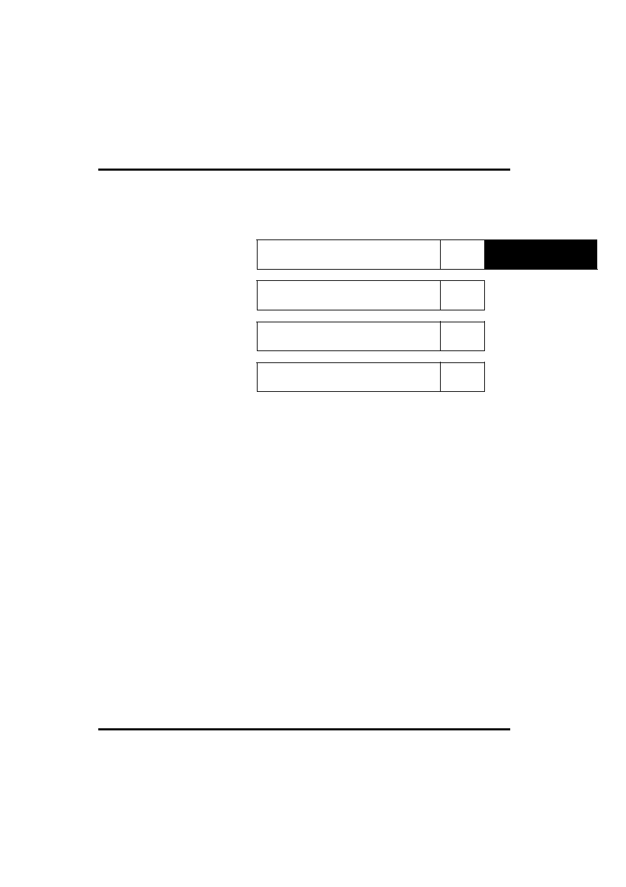
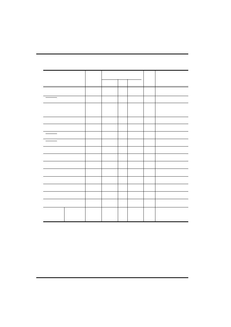
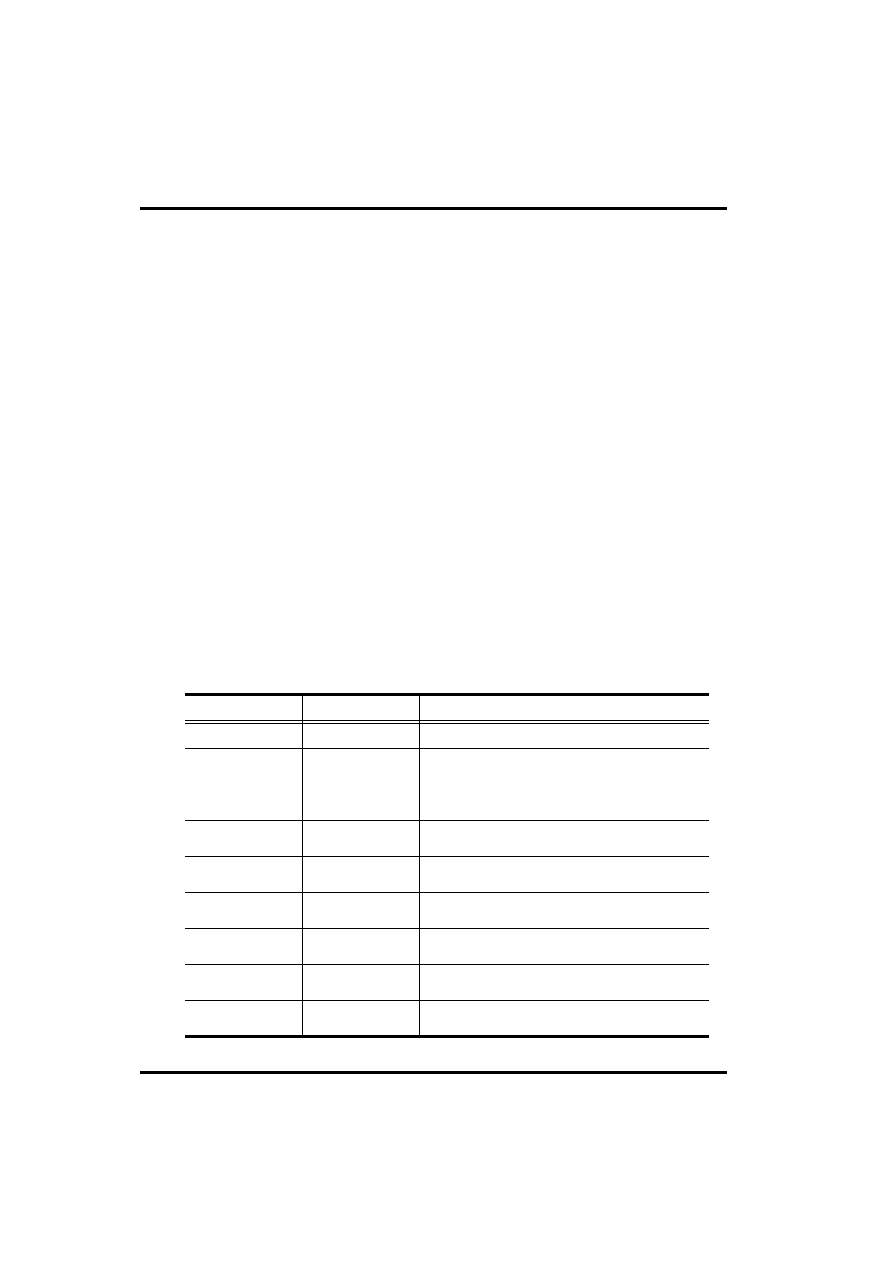
Table 1-1 GMS34XXXT series members
Chapter 1. Introduction
Series
Program memory
Data memory
I/O ports
Input ports
Output ports
Package
KHz version
MHz version
WIDE version
GMS34004T
512
32
¡¿
4
-
4
6
D0 ~ D5
16DIP
GMS34004TK
GMS34004TM
GMS34004TW
GMS34112T
1,024
¡ç
4
¡ç
¡ç
¡ç
20DIP/SOP/SSOP
GMS34112TK
GMS34112TM
GMS34112TW
GMS34140T
¡ç
¡ç
¡ç
¡ç
10
D0 ~ D9
24DIP/SOP
GMS34140TK
GMS34140TM
GMS34140TW
1 - 2
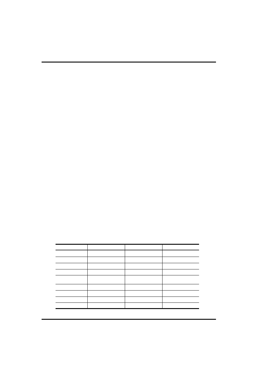
Block Diagram
Fig 1-1 Block Diagram (In case of GMS34140T)
Chapter 1. Introduction
RAM
16word x
2page x 4bit
RAM
Word
Selector
Y-Reg
ACC
ST
R-Latch
D-Latch
Pulse
Generator
X-Reg
MUX
MUX
ALU
23
22
7
8
9
4
21
10
3
5
6
11
12
13
14
15
16
17
18
19
20
Instruction
Decoder
Program counter
Stack
Reset
Watchdog
timer
1
24
2
10
10
8
ROM
64word
¡¿
16page
¡¿
8bit
8
4
4
2
4
10
4
10
4
4
4
16
4
4
4
4
4
OSC1 OSC2
K0 ~ K3
R0 ~ R3
D0 ~ D9
REMOUT
RESET/Vpp
VDD
GND
OSC
Control Signal
1 - 3
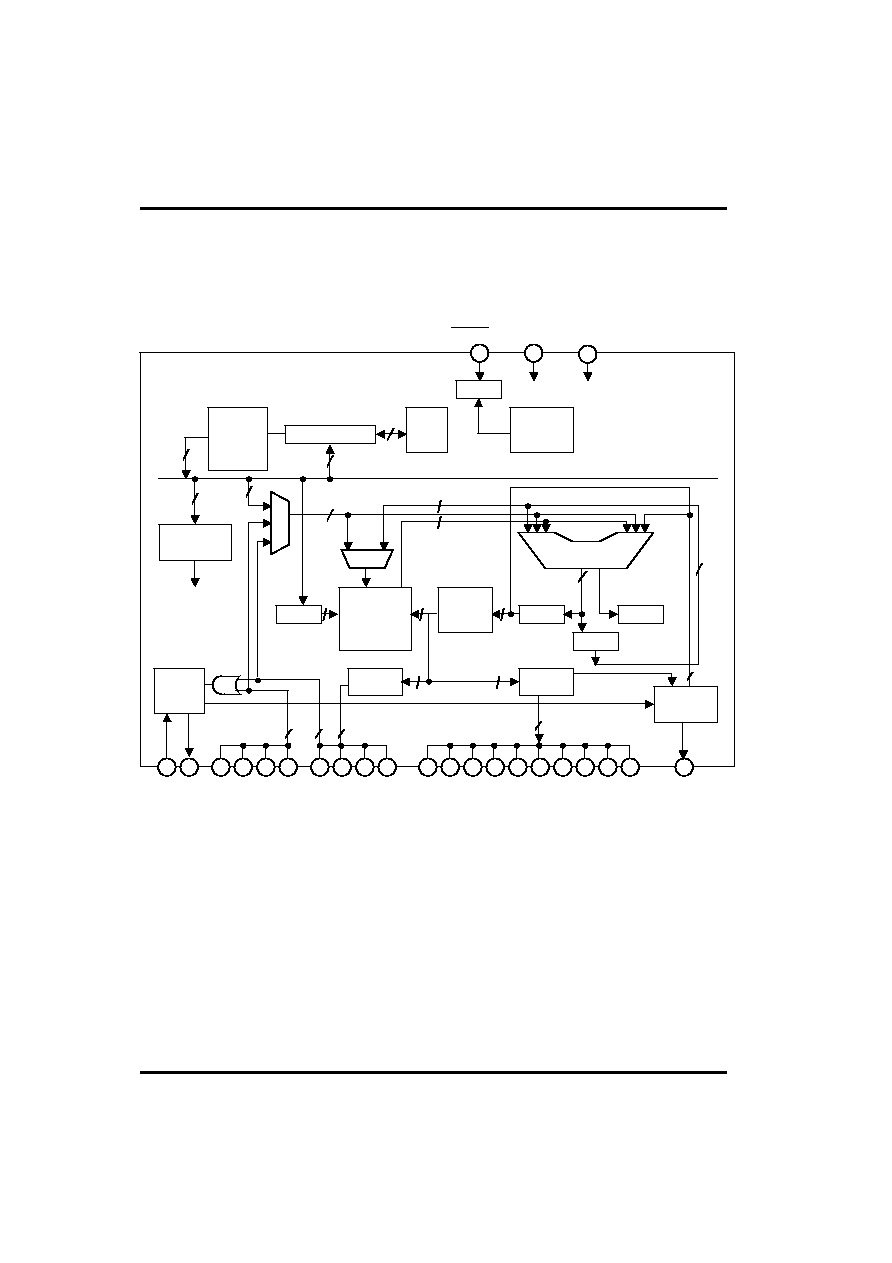
Pin Assignment and terminals
Pin Assignment
Fig 1-2 GMS34004T Pin Assignment
(16PDIP)
Fig 1-3 GMS34112T Pin Assignment
(20DIP/SOP)
Fig 1-4 GMS34112T Pin Assignment
(20SSOP only)
Chapter 1. Introduction
Fig 1-5 GMS34140T Pin Assignment
(24DIP/SOP)
VDD
OSC1
OSC2
REMOUT
D5
D4
D3
D2
RESET/Vpp
GND
K0
K1
K2
K3
D0
D1
1
2
3
4
5
6
7
8
16
15
14
13
12
11
10
9
R3
R2
R1
R0
GND
RESET/Vpp
VDD
OSC1
OSC2
REMOUT
K0
K1
K2
K3
D0
D1
D2
D3
D4
D5
1
2
3
4
5
6
7
8
9
10
20
19
18
17
16
15
14
13
12
11
RESET/Vpp
VDD
OSC1
OSC2
REMOUT
D5
D4
D3
D2
D1
GND
R0
R1
R2
R3
K0
K1
K2
K3
D0
1
2
3
4
5
6
7
8
9
10
20
19
18
17
16
15
14
13
12
11
RESET/Vpp
GND
R0
R1
R2
R3
K0
K1
K2
K3
D0
D8
VDD
OSC1
OSC2
REMOUT
D7
D6
D5
D4
D3
D2
D1
D9
1
2
3
4
5
6
7
8
9
10
24
23
22
21
20
19
18
17
16
15
11
12
14
13
1 - 4
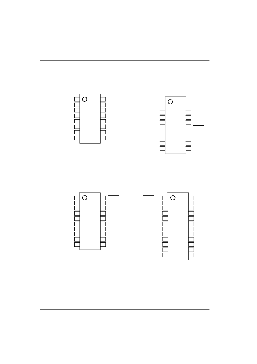
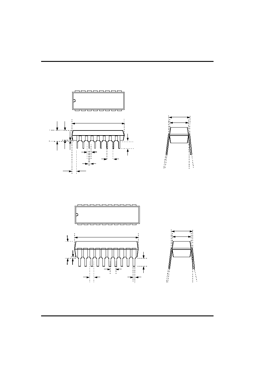
Pin Dimension
Fig 1-6 16PDIP Pin Dimension
1
2
3
4
5
6
7
8
16
15
14
13
12
11
10
9
0.785MAX
0.745MIN
0.040MAX
0.020MIN
0.065MAX
0.015MIN
0.140MAX
0.120MIN
¡æ
¡ç
¡æ ¡ç
0~15
¡Ç
0.260MAX
0.240MIN
0.300BSC
0.014MAX
0.008MIN
Outline (Unit:Inch)
0.050MIN
0.022MAX
0.015MIN
0.100BSC
0.125MIN
0.135MAX
0.170MAX
1
2
3
4
5
6
7
8
9
10
20
19
18
17
16
15
14
13
12
11
0.984MAX
0.968MIN
0.065MAX
0.055MIN
0.022MAX
0.015MIN
0.1TYP
0.170MAX
0.015MIN
0.135MAX
0.125MIN
¡æ
¡ç
¡æ
¡ç
0~15
¡Ç
0.270MAX
0.250MIN
0.3TYP
0.012MAX
0.008MIN
Outline (Unit : Inch)
Fig 1-7 20PDIP Pin Dimension
Chapter 1. Introduction
1 - 5
0.5118MAX
0.4961MIN
0.020MAX
0.014MIN
0.05TYP
0.0118MAX
0.004MIN
1
2
3
4
5
6
7
8
9
10
20
19
1 8 17
16
15
14
13
12
11
¡æ
¡ç
¡æ
¡ç
0.299MAX
0.292MIN
0.419MAX
0.0125MAX
0.0091MIN
0.104MAX
0.093MIN
0.042MAX
0.016MIN
Outline (Unit : Inch)
0.398MIN
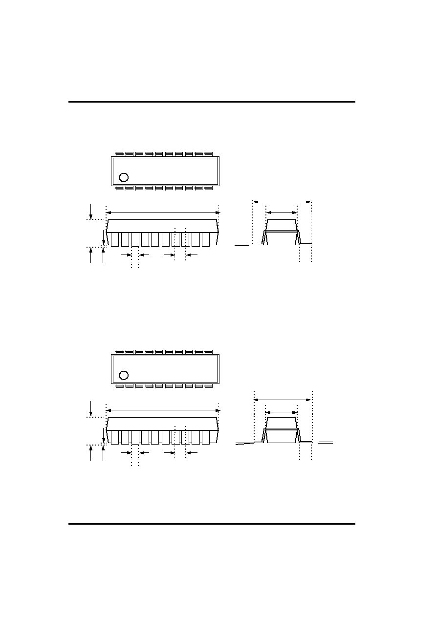
Fig 1-8 20SOP Pin Dimension
Chapter 1. Introduction
0.344MAX
0.337MIN
0.012MAX
0.008MIN
0.025BSC
1
2
3
4
5
6
7
8
9
10
20
19
1 8 17
16
15
14
13
12
11
¡æ
¡ç
¡æ
¡ç
0.010MAX
0.007MIN
0.032MAX
0.022MIN
Outline (Unit : Inch)
Fig 1-9 20SSOP Pin Dimension
0.244MAX
0.234MIN
0.157MAX
0.150MIN
0.066MAX
0.057MIN
0.010MAX
0.004MIN
0-8
¢ª
¡é
¡è
1 - 6
Chapter 1. Introduction
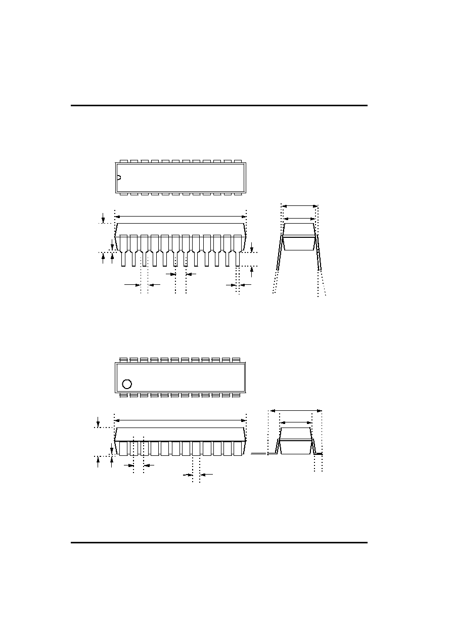
Fig 1-11 24SOP Pin Dimension
1
2
3
4
5
6
7
8
9
10
11
12
24
23
22
21
20
19
18
17
16
15
14
13
1.255MAX
1.245MIN
0.065MAX
0.055MIN
0.022MAX
0.015MIN
0.1TYP
0.015MIN
0.135MAX
0.125MIN
¡æ
¡ç
¡æ
¡ç
0~15
¢ª
0.270MAX
0.250MIN
0.3TYP
0.012MAX
0.008MIN
Outline (Unit : Inch)
Fig 1-10 24Skinny DIP Pin Dimension
0.170MAX
0.616MAX
0.595MIN
0.020MAX
0.014MIN
0.05TYP
0.018MAX
0.004MIN
1
2
3
4
5
6
7
8
9
10
11
12
24
23
22
21
20
19
18
17
16
15
14
13
¡æ
¡ç
¡æ
¡ç
0.299MAX
0.292MIN
0.419MAX
0.398MIN
0.0125MAX
0.0091MIN
0.042MAX
0.016MIN
Outline (Unit : Inch)
0.104MAX
0.093MIN
1 - 7
Pin
Function
Pin Description and Circuit
Pin Description
I/O
Connected to 2.2~4.5V power supply at KHz and MHz
version or 4.0 ~ 5.5V power supply at WIDE version.
Connected to 0V power supply.
Used to input a manual reset. When the pin goes "L",
the D-output ports and REMOUT-output port are initialized to
"L", and ROM address is set to address 0 on page 0.
For programming, this pin receives 12.5V programming
voltage.
4-bit input port.
STOP mode is released by "L" input of each pin.
The output is the structure of N-channel-open-drain.
4-bit I/O port. (Input mode is set only when each of them
output "H".)
In outputting, each can be set and reset independently(or at
once.)
The output is in the form of C-MOS.
STOP mode is released by "L" input of each pin.
High current output port.
The output is in the form of C-MOS.
The state of large current on is "H".
Oscillator input. Input to the oscillator circuit and connection
point for ceramic resonator.
Internal capacitors available at KHz version.
A feedback resistor is connected between this pin and OSC2.
Connect a resonator between this pin and OSC1.
V
DD
GND
RESET
K0~K3
D0~D9
R0~R3
REMOUT
OSC1
OSC2
Input
Input
Output
I/O
Output
Input
Output
-
-
Chapter 1. Introduction
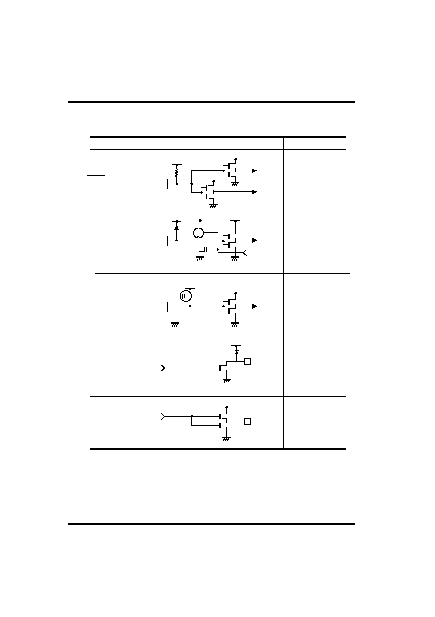
1 - 8
I/O circuit types and options
Hysteresis Input Type.
Built in pull-up-resistor,
Typical 800
§Ú
Reset/Vpp
I
Pin
I/O
Note
¡æ
¡ç
¡æ
¡ç
CMOS output.
"H" output at reset.
Built in MOS Tr for
pull-up about 120
§Ú
.
R0~R3
I/O
Built in MOS Tr for
pull-up About 120
§Ú
.
K0~K3
I
Open drain output.
"L" output at reset.
D0~D9
O
¡æ
¡ç
CMOS output.
"L" output at reset.
High current output
source.
REMOUT
O
I/O circuit
¡ç
¡æ
¡ç
¡æ
¡ç
¡æ
¡ç
¡æ
pull-up
Chapter 1. Introduction
pull-up
1 - 9
Built in feedback-resistor
about 1
§Û
OSC2
O
Pin
I/O
Note
Built in resonance
Capacitor at KHz version
C1=C2 = 100pF
¡¾
15%
[C1,C2 are not available
for MHz and WIDE
version]
OSC1
I
I/O circuit
Built in damping-resistor
Rd = 4
§Ú
[No resistor in MHz
operation]
¡æ
¡ç
¡æ
¡ç
¡è
¡è
OSC2
Rd
C2
Rf
C1
OSC1
STOP
Chapter 1. Introduction
Frequency
Resonator Maker
Part Name
Load Capacitor
320KHz
CQ
ZTB320D
C1=C2=Open
ZTB500E
C1=C2=Open
500KHz
CQ
3.43MHz
CQ
ZTA3.43MG
C1=C2=30pF
TDK
FCR3.52M5
C1=C2=33pF
CQ
ZTA3.64MG
C1=C2=30pF
3.84MHz
TDK
FCR3.64M5
C1=C2=33pF
CQ
ZTA3.84MG
C1=C2=30pF
TDK
FCR3.84M5
C1=C2=33pF
CQ recommend 430KHz~500KHz resonator
3.52MHz
3.64MHz
4.00MHz
CQ
ZTA4.00MG
C1=C2=30pF
1 - 10
Parameter
Supply Voltage
Programming Voltage
Power dissipation
Storage temperature range
Input voltage
Output voltage
Unit
V
V
mW
¡É
V
V
Electrical Characteristics
Absolute maximum ratings (Ta = 25
¡É
)
Symbol
V
DD
V
PP
P
D
Tstg
V
IN
V
OUT
Max. rating
-0.3 ~ 7.0
-0.3 ~ 13.5
700 *
-55 ~ 125
-0.3 ~ V
DD
+0.3
-0.3 ~ V
DD
+0.3
* Thermal derating above 25
¡É
: 6mW per degree
¡É
rise in temperature.
Parameter
Supply Voltage
Operating temperature
Unit
V
¡É
Recommended operation condition
Rating
2.2 ~ 4.5
2.2 ~ 4.5
4.0 ~ 5.5
-20 ~ +70
Chapter 1. Introduction
Condition
300 ~ 500KHz
2.4 ~ 4MHz
300KHz ~ 4.2MHz
-
Symbol
V
DD
Topr
1 - 11
Electrical characteristics for low voltage products (Ta=25
¡É
, V
DD
=3V)
Chapter 1. Introduction
Parameter
Symbol
Limits
Unit
Condition
f
OSC
/6
f
OSC
/48
f
OSC
Input H current
RESET input L current
K, R input L current
K, R input H voltage
RESET input H voltage
RESET input L voltage
D. R output L voltage
REMOUT output L voltage
REMOUT output H voltage
OSC2 output L voltage
OSC2 output H voltage
D, R output leakage current
Current on STOP mode
Operating supply current 1
Operating supply current 2
System
clock
frequency
K, R input L voltage
f
OSC
I
DD2
*
I
DD1
*
I
STOP
I
OL
V
OH3
V
OL3
V
OH1
V
OL2
V
IL2
V
IH2
V
IL1
V
IH1
I
IL1
I
IL2
I
IH
V
OL1
2.4
300
-
-
-
-
2.1
-
2.1
-
-
2.25
-
2.1
-9
-2
-
-
-
-
0.5
0.3
-
-
2.5
0.4
2.5
0.15
-
-
-
-
-25
-7.5
-
0.15
Min.
Typ.
Max.
4
500
4.0
4.0
1
1
-
0.9
-
0.4
0.75
-
0.9
-
-50
-16
1
0.4
MHz
KHz
mA
mA
uA
uA
V
V
V
V
V
V
V
V
uA
uA
uA
V
f
OSC
=4MHz
f
OSC
=455KHz
At STOP mode
V
0UT
=V
DD
, Output off
I
OH
=70uA
I
OL
=70uA
I
OH
=-8mA
I
OL
=1mA
V
-
-
-
VI=GND, Output
off, Pull-Up resistor
provided.
VI=GND
VI=V
DD
I
OL
=100uA
KHz version
MHz version
* I
DD1
, I
DD2
, is measured at RESET mode.
1 - 12
Parameter
Electrical characteristics (Ta=25
¡É
, V
DD
=5V)
Symb
ol
Limits
Unit
Condition
f
OSC
/6
Input H current
RESET input L current
K, R input L current
K, R input H voltage
RESET input H voltage
RESET input L voltage
D. R output L voltage
REMOUT output L voltage
REMOUT output H voltage
OSC2 output L voltage
OSC2 output H voltage
D, R output leakage current
Current on STOP mode
Operating supply current
System
clock
frequency
K, R input L voltage
f
OSC
I
DD
I
STOP
I
OL
V
OH3
V
OL3
V
OH1
V
OL2
V
IL2
V
IH2
V
IL1
V
IH1
I
IL1
I
IL2
I
IH
V
OL1
0.3
-
-
-
V
DD
-1.0
-
V
DD
-1.0
-
-
0.75*V
DD
-
0.7*V
DD
-9
-2
-
-
-
-
-
-
-
-
-
-
-
-
-
-
-
-
-
-
Min.
Typ.
Max.
4.2
10
10
5
-
0.9
-
0.4
0.25*V
DD
-
0.3*V
DD
-
-150
-20
5
0.4
MHz
mA
uA
uA
V
V
V
V
V
V
V
V
uA
uA
uA
V
At RESET mode
At STOP mode
V
0UT
=V
DD
, Output off
I
OH
=-70uA
I
OL
=70uA
I
OH
=-8mA
I
OL
=2mA
V
-
-
-
VI=GND, Output
off, Pull-Up resistor
provided.
VI=GND
VI=V
DD
I
OL
=100uA
WIDE version
Chapter 1. Introduction
INTRODUCTION
1
ARCHITECTURE
2
INSTRUCTION
3
EPROM
4
2 - 1
CHAPTER 2. Architecture
BLOCK DESCRIPTION
Program Memory (EPROM)
The GMS34XXXT series can incorporate maximum 1,024 words (64 words
¡¿
16
pages
¡¿
8bits) for program memory. Program counter PC (A0~A5) and page
address register (A6~A9) are used to address the whole area of program
memory having an instruction (8bits) to be next executed.
The program memory consists of 64 words on each page, and thus each page
can hold up to 64 steps of instructions.
The program memory is composed as shown below.
0 1
2 3
4 5
6 7
8
63
Program counter (PC)
Page address register (PA)
Page buffer (PB)
6
4
(Level "1")
(Level "2")
(Level "3")
(PSR)
(SR)
Stack register
Page 0
Page 1
Page 2
Page 15
A0~A5
0
1
2
15
A6~A9
Program capacity (pages)
Fig 2-1 Configuration of Program Memory
Chapter 2. Architecture
4

2 - 2
EPROM Address Register
The following registers are used to address the EPROM.
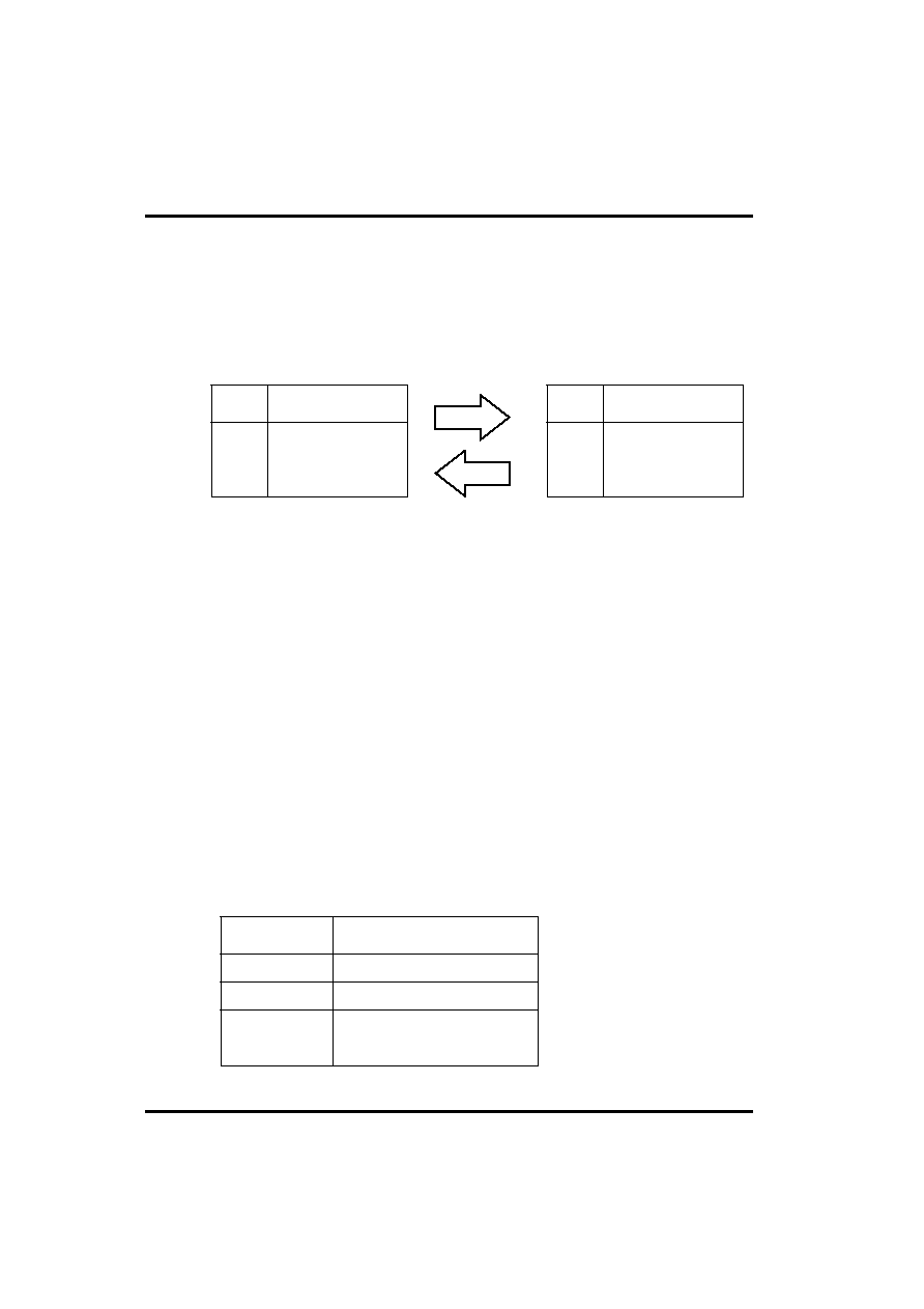
· Page address register (PA) :
Holds EPROM's page number (0~Fh) to be addressed.
· Page buffer register (PB) :
Value of PB is loaded by an LPBI command when newly addressing a page.
Then it is shifted into the PA when rightly executing a branch instruction (BR)
and a subroutine call (CAL).
· Program counter (PC) :
Available for addressing word on each page.
· Stack register (SR) :
Stores returned-word address in the subroutine call mode.
(1) Page address register and page buffer register :
Address one of pages #0 to #15 in the EPROM by the 4-bit binary counter.
Unlike the program counter, the page address register is usually unchanged
so that the program will repeat on the same page unless a page changing
command is issued. To change the page address, take two steps such as
(1) writing in the page buffer what page to jump (execution of LPBI) and
(2) execution of BR or CAL, because instruction code is of eight bits so
that page and word can not be specified at the same time.
In case a return instruction (RTN) is executed within the subroutine that has
been called in the other page, the page address will be changed at the
same time.
(2) Program counter :
This 6-bit binary counter increments for each fetch to address a word in the
currently addressed page having an instruction to be next executed.
For easier programming, at turning on the power, the program counter is
reset to the zero location. The PA is also set to "0". Then the program
counter specifies the next EPROM address in random sequence.
When BR, CAL or RTN instructions are decoded, the switches on each step
are turned off not to update the address. Then, for BR or CAL, address
data are taken in from the instruction operands (a
0
to a
5
), or for RTN, and
address is fetched from stack register No. 1.
(3) Stack register :
This stack register provides two stages each for the program counter (6
bits) and the page address register (4bits) so that subroutine nesting can be
made on two levels.
Chapter 2. Architecture
2 - 3
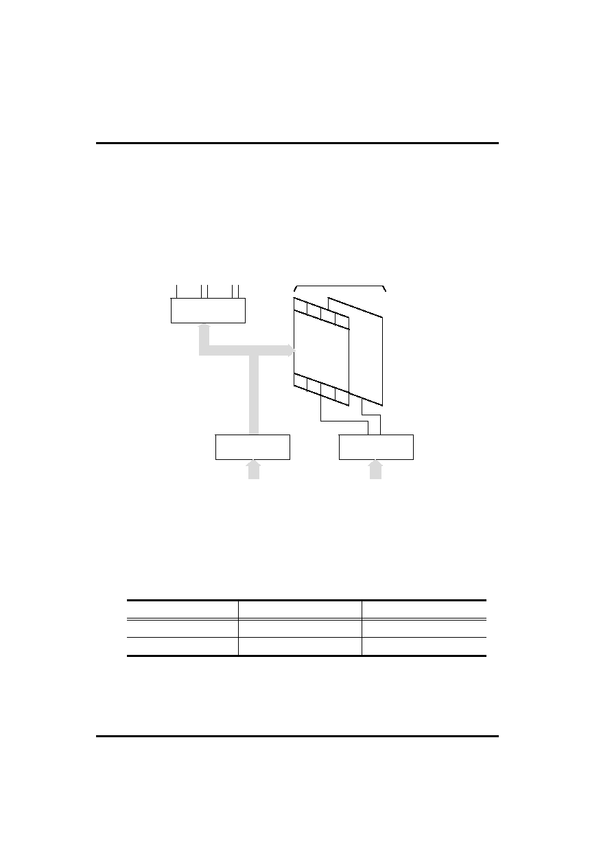
Data memory (RAM)
Up to 32 nibbles (16 words
¡¿
2pages
¡¿
4bits) is incorporated for storing data.
The whole data memory area is indirectly specified by a data pointer (X,Y). Page
number is specified by zero bit of X register, and words in the page by 4 bits in
Y-register. Data memory is composed in 16 nibbles/page. Figure 2-2 shows the
configuration.
0
1
2
3
15
Output port
Y-register (Y)
X-register (X)
D0
D9 R0
R3 REMOUT
Page 0
Page 1
0
1
4
A0~A3
Data memory page (0~1)
X-register (X)
X-register is consist of 2bit, X0 is a data pointer of page in the RAM, X1 is only
used for selecting of D8~D9 with value of Y-register
Fig 2-2 Composition of Data Memory
X1=1
X1=0
D8
D9
Y=0
Y=1
D1
D0
Table 2-1 Mapping table between X and Y register
Chapter 2. Architecture
4
2

2 - 4
Y-register (Y)
Y-register has 4 bits. It operates as a data pointer or a general-purpose register.
Y-register specifies and address (a
0
~a
3
) in a page of data memory, as well as it
is used to specify an output port. Further it is used to specify a mode of carrier
signal outputted from the REMOUT port. It can also be treated as a general-
purpose register on a program.
Accumulator (A
CC
)
The 4-bit register for holding data and calculation results.
Arithmetic and Logic Unit (ALU)
In this unit, 4bits of adder/comparator are connected in parallel as it's main
components and they are combined with status latch and status logic (flag.)
(1) Operation circuit (ALU) :
The adder/comparator serves fundamentally for full addition and data
comparison. It executes subtraction by making a complement by processing
an inversed output of A
CC
(A
CC
+1)
(2) Status logic :
This is to bring an ST, or flag to control the flow of a program. It occurs when
a specified instruction is executed in three cases such as overflow or
underflow in operation and two inputs unequal.
Chapter 2. Architecture
2 - 5
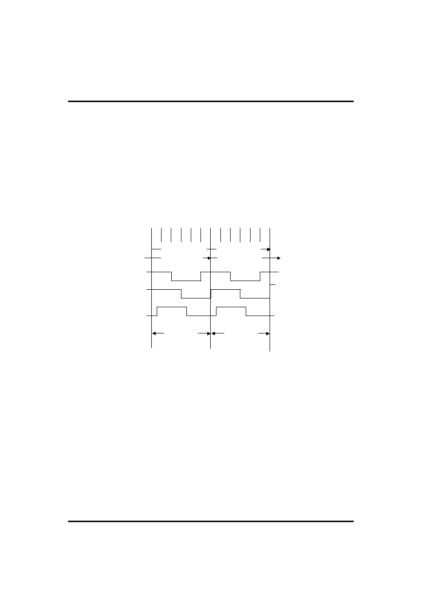
State Counter (SC)
A fundamental machine cycle timing chart is shown below. Every instruction is
one byte length. Its execution time is the same. Execution of one instruction
takes 6 clocks for fetch cycle and 6 clocks for execute cycle (12 clocks in total).
Virtually these two cycles proceed simultaneously, and thus it is apparently
completed in 6 clocks (one machine cycle). Exceptionally BR, CAL and RTN
instructions is normal execution time since they change an addressing
sequentially. Therefore, the next instruction is prefetched so that its execution
is completed within the fetch cycle.
T1 T2 T3 T4 T5 T6 T1 T2 T3 T4 T5 T6
Fetch cycle N
Execute cycle N-1
Execute cycle N
Fetch cycle N-1
Machine
Cycle
Machine
Cycle
Phase
¥°
Phase
¥±
Phase
¥²
Fig. 2-3 Fundamental timing chart
Chapter 2. Architecture
2 - 6
Clock Generator
The GMS34XXXT series has an internal clock oscillator. The oscillator circuit is
designed to operate with an external ceramic resonator. Internal capacitors are
available at KHz version. Oscillator circuit is able to organize by connecting
ceramic resonator to outside.
* It is necessary to connect capacitor to outside in order to change ceramic
resonator, you must refer to a manufacturer`s resonator matching guide.
OSC1
OSC2
C1
C2
<Circuit 1>
23
22
OSC1
OSC2
<Circuit 2>
23
22
Oscillation Circuit
Operating Frequency
Chapter 2. Architecture
Version
KHz
MHz
WIDE
300KHz ~ 500KHz
2.4MHz ~ 4MHz
300KHz ~ 4.2MHz
Circuit 2
Circuit 1
Circuit 1
Circuit 1
Internal capacitor
No Internal capacitor
No Internal capacitor
No Internal capacitor
2 - 7
Pulse generator
The following frequency and duty ratio are selected for carrier signal outputted
from the REMOUT port depending on a PMR (Pulse Mode Register) value set in
a program.
T
T1
REMOUT signal
T=1/f
PUL
= 12/f
OSC
[96/f
OSC
],
T1/T = 1/2
0
1
PMR
2
3
4
5
T=1/f
PUL
= 12/f
OSC
[96/f
OSC
],
T1/T = 1/3
T=1/f
PUL
= 8/f
OSC
[64/f
OSC
],
T1/T = 1/2
T=1/f
PUL
= 8/f
OSC
[64/f
OSC
],
T1/T = 1/4
T=1/f
PUL
= 11/f
OSC
[88/f
OSC
],
T1/T = 4/11
No Pulse (same to D0~D9)
* Default value is "0"
* [ ] means the value of "T", when Instruction cycle is f
OSC
/48 in MHz version
Table 2-2 PMR selection table
6
T=1/f
PUL
= 12/f
OSC
[96/f
OSC
],
T1/T = 1/4
Chapter 2. Architecture
7
No pulse (same to D0 ~ D9)
2 - 8
Initial Reset Circuit
RESET pin must be down to "L" more than 4 machine cycle by outside
capacitor or other for power on reset.
The mean of 1 machine cycle is 6/f
OSC
or 48/f
OSC
, however, operating voltage
must be in recommended operating conditions, and clock oscillating stability.
* It is required to adjust C value depending on rising time of power supply.
(Example shows the case of rising time shorter than 10ms.)
1
RESET
0.1uF
Chapter 2. Architecture
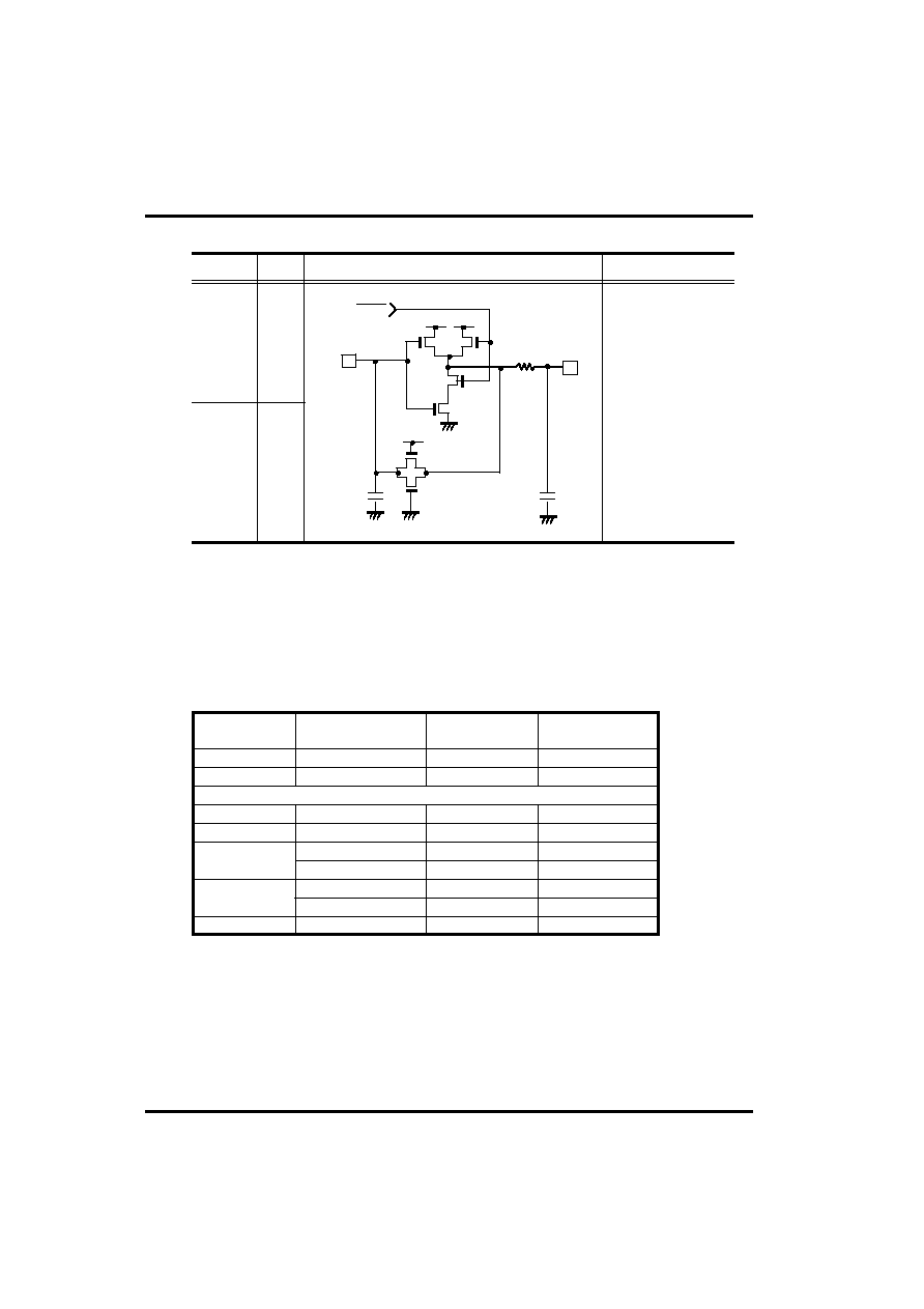
Watch Dog Timer (WDT)
Watch dog timer is organized binary of 14 steps. The signal of f
OSC
/6 cycle comes
in the first step of WDT after WDT reset. If this counter was overflowed, reset
signal automatically come out so that internal circuit is initialized.
The overflow time is 6
¡¿
2
13
/f
OSC
(108.026ms at f
OSC
=455KHz.)
8
¡¿
6
¡¿
2
13
/f
OSC
(108.026ms at f
OSC
= 3.64MHz)
Normally, the binary counter must be reset before the overflow by using reset
instruction (WDTR) or / and REMOUT port HIGH(Y-reg=8, So instruction execution).
* It is constantly reset in STOP mode. When STOP is released, counting is
restarted. (Refer to 2-9 STOP function>)
Binary counter
(14 steps)
RESET (edge-trigger)
f
OSC
/6 or f
OSC
/48
CPU reset
Reset
by instruction
REMOUT
output
2 - 9
STOP Operation
Stop mode can be achieved by STOP instructions.
In stop mode :
1. Oscillator is stopped, the operating current is low.
2. Watch dog timer is reset, D8~D9 output and REMOUT output are "L".
3. Part other than WDT, D8~D9 output and REMOUT output have a value before
come into stop mode.
Stop mode is released when one of K or R input is going to "L".
1. State of D0~D7 output and REMOUT output is return to state of before stop mode
is achieved.
2. After 1,024
¡¿
8 enable clocks for stable oscillating, First instruction start to operate.
3. In return to normal operation, WDT is counted from zero again.
But, at executing stop instruction, if one of K or R input is chosen to "L", stop instruction
is same to NOP instruction.
Port Operation
Value of X-reg
Value of X-reg
0 or 1
0 ~ 7
S0 : D(Y)
¡ç
1,
R0 : D(Y)
¡ç
0
Operation
0 or 1
8
REMOUT port repeats "H" and "L" in pulse
frequency. (When PMR = 5, it is fixed at "H")
S0 : REMOUT(PMR)
¡ç
1
R0 : REMOUT(PMR)
¡ç
0
0 or 1
9
S0 : D0 ~ D9
¡ç
1 (High-Z)
R0 : D0 ~ D9
¡ç
0
0 or 1
A ~ D
S0 : R(Y-Ah)
¡ç
1
R0 : R(Y-Ah)
¡ç
0
0 or 1
E
S0 : R0 ~ R3
¡ç
1
R0 : R0 ~ R3
¡ç
0
0 or 1
F
S0 : D0 ~ D9
¡ç
1, R0 ~ R3
¡ç
1
R0 : D0 ~ D9
¡ç
0, R0 ~ R3
¡ç
0
2 or 3
0
S0 : D(8)
¡ç
1
R0 : D(8)
¡ç
0
2 or 3
1
S0 : D(9)
¡ç
1
R0 : D(9)
¡ç
0
Chapter 2. Architecture
INTRODUCTION
1
ARCHITECTURE
2
INSTRUCTION
3
EPROM
4
3 - 1
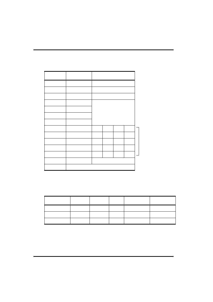
Chapter 3. Instruction
CHAPTER 3. Instruction
Instruction Table
The GMS34XXXT series provides the following 43 basic instructions.
Category
1
2
3
Register to
Register
LAY
LYA
LAZ
Mnemonic
A
¡ç
Y
Function
Y
¡ç
A
A
¡ç
0
S
S
S
ST
*1
4
5
6
RAM to
Register
LMA
LMAIY
LYM
M(X,Y)
¡ç
A
M(X,Y)
¡ç
A, Y
¡ç
Y+1
Y
¡ç
M(X,Y)
S
S
S
7
8
LAM
XMA
A
¡ç
M(X,Y)
A
¡ê
M(X,Y)
S
S
9
10
11
Immediate
LYI i
LMIIY i
LXI n
Y
¡ç
i
M(X,Y)
¡ç
i, Y
¡ç
Y+1
X
¡ç
n
S
S
S
12
13
14
RAM Bit
Manipulation
SEM n
REM n
TM n
M(n)
¡ç
1
M(n)
¡ç
0
TEST M(n) = 1
S
S
E
15
16
17
ROM
Address
BR a
CAL a
RTN
if ST = 1 then Branch
if ST = 1 then Subroutine call
Return from Subroutine
S
S
S
18
LPBI i
PB
¡ç
i
S
19
20
21
Arithmetic
AM
SM
IM
A
¡ç
A + M(X,Y)
A
¡ç
M(X,Y) - A
A
¡ç
M(X,Y) + 1
C
B
C
22
23
DM
IA
A
¡ç
M(X,Y) - 1
A
¡ç
A + 1
B
S
24
25
IY
DA
Y
¡ç
Y + 1
A
¡ç
A - 1
C
B
3 - 2
Chapter 3. Instruction
Category
26
27
28
Arithmetic
DY
EORM
NEGA
Mnemonic
Y
¡ç
Y - 1
Function
A
¡ç
A + M (X,Y)
A
¡ç
A + 1
B
S
Z
ST
*1
29
30
Comparison
ALEM
ALEI i
TEST A
¡Â
M(X,Y)
TEST A
¡Â
i
E
E
31
32
MNEZ
YNEA
TEST M(X,Y)
¡Á
0
TEST Y
¡Á
A
N
N
33
34
YNEI i
KNEZ
TEST Y
¡Á
i
TEST K
¡Á
0
N
N
35
RNEZ
TEST R
¡Á
0
N
36
37
Input /
Output
LAK
LAR
A
¡ç
K
A
¡ç
R
S
S
38
39
SO
RO
Output(Y)
¡ç
1
*2
Output(Y)
¡ç
0
*2
S
S
40
41
Control
WDTR
STOP
Watch Dog Timer Reset
Stop operation
S
S
42
43
LPY
NOP
PMR
¡ç
Y
No operation
S
S
Note) i = 0~f, n = 0~3, a = 6bit PC Address
*1 Column ST indicates conditions for changing status. Symbols have the following
meanings
S : On executing an instruction, status is unconditionally set.
C : Status is only set when carry or borrow has occurred in operation.
B : Status is only set when borrow has not occurred in operation.
E : Status is only set when equality is found in comparison.
N : Status is only set when equality is not found in comparison.
Z : Status is only set when the result is zero.
*2 Operation is settled by a value of Y-register.
INTRODUCTION
1
ARCHITECTURE
2
INSTRUCTION
3
EPROM
4

4 - 1
Chapter 4. EPROM
CHAPTER 4. EPROM
GMS34004TK / 34112TK / 34140TK
Mode define
Device operation
Exact User pgm
Address in, Data out
Item
User mode
EPROM read mode
EPROM
Program
mode
1Byte PGM Write
2Byte PGM Write
Program verify
Lock bit Write
Lock bit Read
Address in, Data in
Address in, Data in
Address in, Data out
Lock bit write(set D5 to 1)
Lock bit out
Mode setting
RESETB = 0 ~ 3V
Vcc=3V
Vcc=6.0V
Vcc=6.0V
K3~0=0110
K3~0=0110
K3~0=0111
-
K3~0=0100
K3~0=0101
RESETB
=12.5V
RESETB
=12.5V
Lock bit
Program
mode
RESETB
=12.5V
Vcc=6.0V,
Lock bit is D5.
(Default : unlock)

4 - 2
Port define
Chapter 4. EPROM
NMOS open drain I/O
in EPROM mode
* Undefined ports in this table are N.C (No Connection)
Port Name
VDD
RESETB
OSC1
K0
K1
K2
K3
User Mode
3.0V
Reset (0, 3.0V)
Clock input
K0(Input)
K1(Input)
K2(Input)
K3(Input)
EPROM Mode
6.0V
Vpp (0, 12.5V)
Clock input
Read / Write Control
Address / Data Control
D0
D1
D2
D3
D4
D5
D0(Output)
D1(Output)
D2(Output)
D3(Output)
D4(Output)
D5(Output)
A0
A5
Da0
Da4
Lock bit output
GND
0V
A1
A6
Da1
Da5
A2
A7
Da2
Da6
A3
A8
Da3
Da7
A4
A9
-
-
Programming data
Device Name
GMS34004TK
ROM Size
512bytes
Blank data
(HEX)
FF
Lock bit
Yes
Device address
0000 ~ 01FF
File address
0000 ~ 01FF
GMS34112TK
1,024bytes
FF
Yes
0000 ~ 03FF
0000 ~ 03FF
GMS34140TK
1,024bytes
FF
Yes
0000 ~ 03FF
0000 ~ 03FF
- If lock bit is set, the EPROM of the device can not be read, because output is always FF.
- Input file : Intel Hexa format ( *.RHX )
4 - 3
Chapter 4. EPROM
Write / Read data conversion
- You must change MSB ~ LSB
¡ê
LSB ~ MSB.
- Example
Hex
Binary (MSB~LSB)
2C
E4
8D
0010 1100
1110 0100
1000 1101
Write
Read
Hex
Binary (MSB~LSB)
34
27
B1
0011 0100
0010 0111
1011 0001
File / buffer data
Device (D3 ~ D0)
Checksum
- It is calculated from the Buffer of the programmer.
- Address range is the same as device address.
- Calculate method is the same as normal EPROM devices (ex:27C128, 256 etc)
Programming control
- OSC1 & RESETB control OTP device, so you must count OSC1 clocks in every state.
- K ports control the internal state of the OTP device(ex: Read, Write...).
- D5~D0 ports are NMOS open drain I/O in EPROM mode.
It must be pulled up by resistors (about 4.7~ 47K ohm).
- The frequency rate of the OSC1 clock is 10KHz ~ 500KHz.
You can hold OSC1 HIGH or LOW state when you need.
Item
Range
VCC
0 ~ 6.0V
¡¾
0.25V
Programming DC specification
RESETB
0 ~ 12.5V
¡¾
0.5V
K-port
D-port
0 ~ 0.2VCC(Low)
0.8VCC ~ VCC (High)
4 - 4
Chapter 4. EPROM
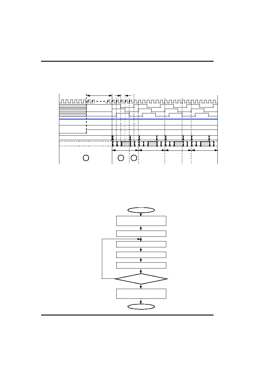
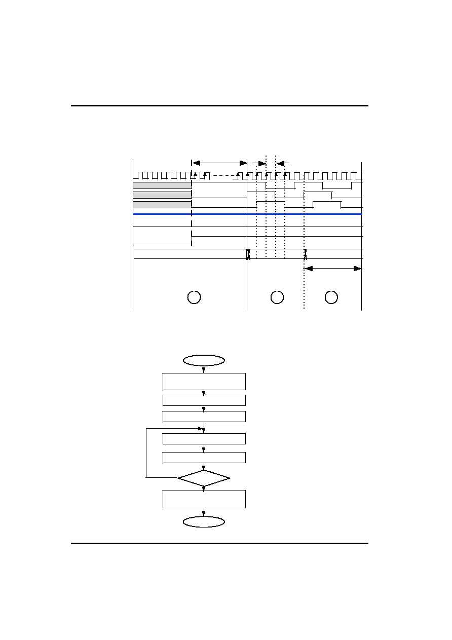
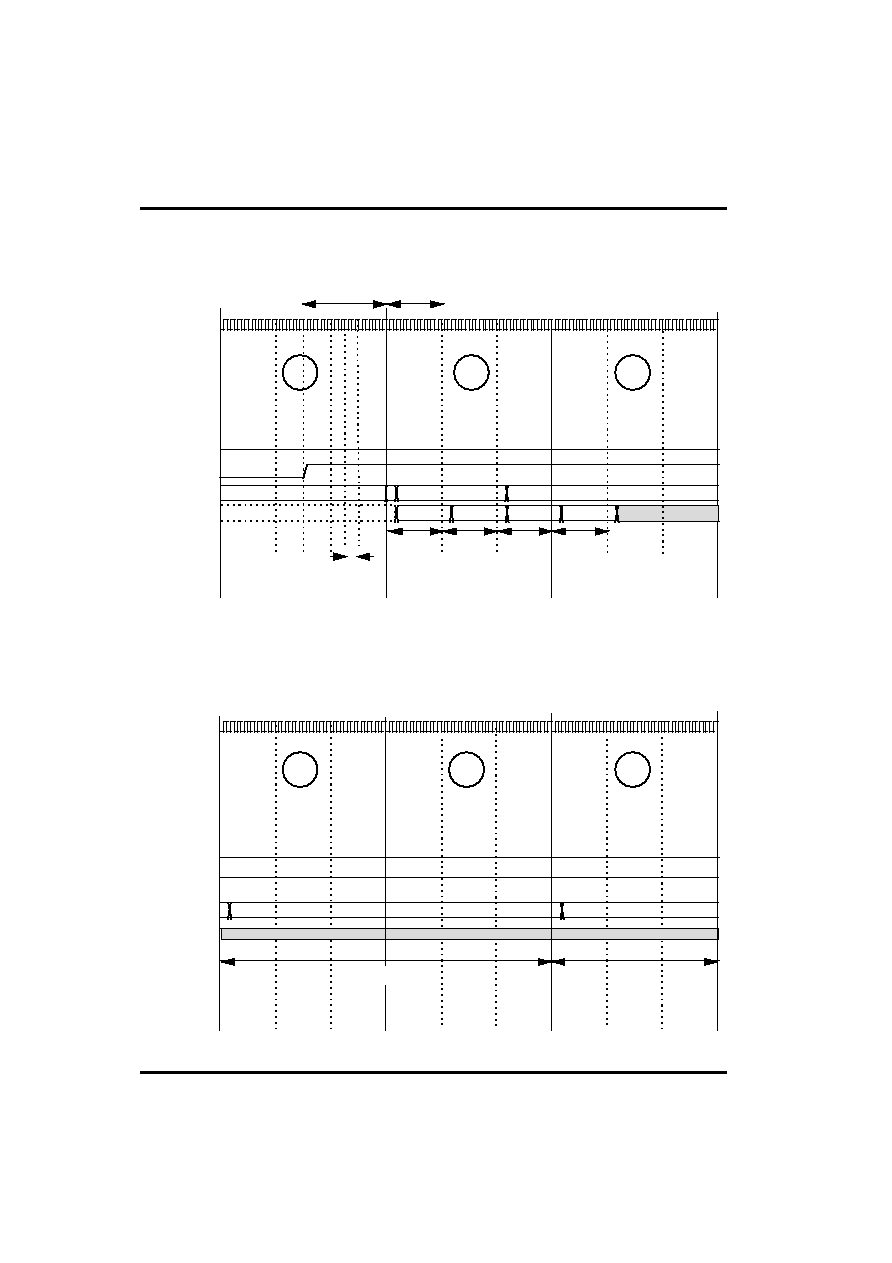
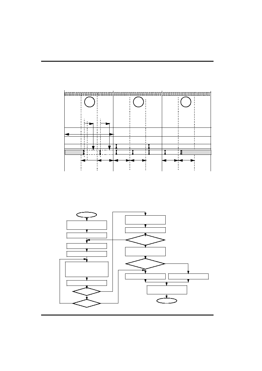
EPROM read mode (1/2)
AL : Low Address (A4~0) Input Latch
OH : High Data (D7~4) Output
OL : Low Data (D3~0) Output
AH : High Address (A9~5) Input Latch
For device verify or read.
If you set Lock bit, output data is always FF.
* Note : 1. AH, AL, DH, DL Inputs released at 100~200nS after OSC rising edge and
width is 1OSC cycle ( if OSC is 500KHz, width is 2uS ).
RESETB
OSC
12.5V
CK1
CK2
CK3
K3 ~ K0
0110
AH
D4 ~ D0
0000
VCC
6V
0V
AL
OH
OL
1101
AH
AL
OH
OL
AH
AL
OH
OL
AH
AL
OH
OL
0000
1101
0000
1101
0000
1101
Addr. 0
Addr. 1
Addr. 2
Addr. 3
1
2
3
2us at 500KHz
¨ç ¨è
¨õ
¨ô
14.5clocks
EPROM read mode (2/2)
START
END
¨ç
Reset
(Set EPROM read mode)
Address=First address
¨è
Set address
¨é
Read data
Address ++
Address > Last address
RESETB=0V
VCC=0V
4 - 5
Chapter 4. EPROM
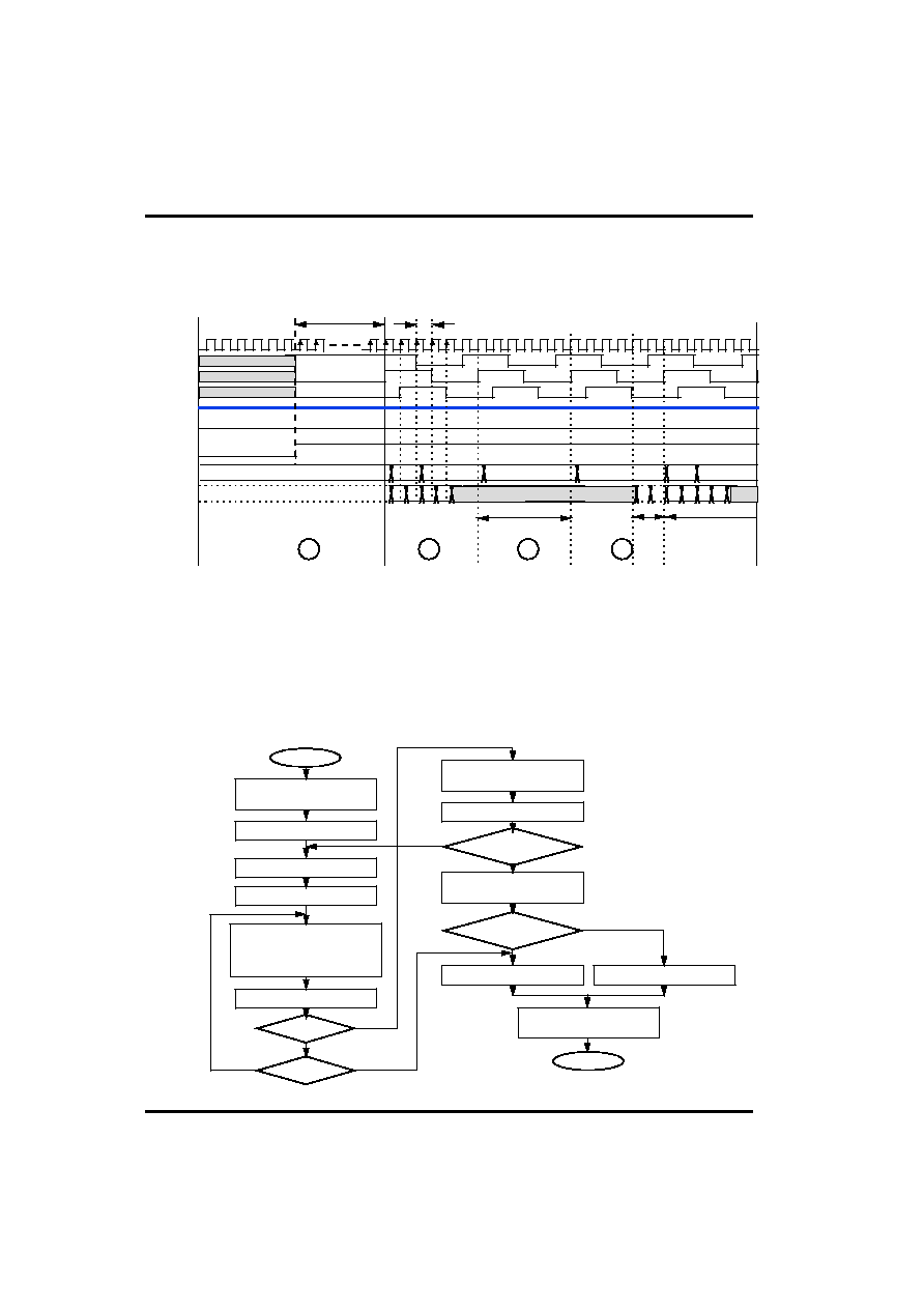
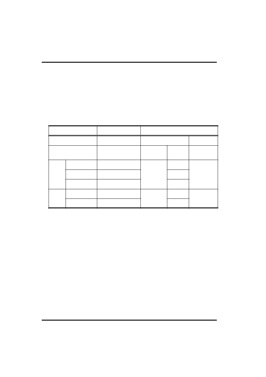
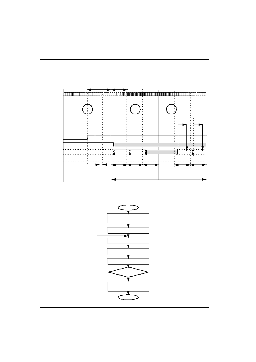
EPROM write mode (1/2)
RESETB
OSC
12.5V
CK1
CK2
CK3
K3 ~ K0
PGM Write ( 0110 )
AH
D4 ~ D0
0000
1101
VCC
6V
0V
1000
1110
0000
1000
AL
DH
DL
AH
AL
DH
DL
OH
OL
10times Repeat
12us X 10 = 120us
Verify
Next Write
AH : High bit Address Input Latch
AL : Low bit Address Input Latch
DH : High bit Data Input Latch
DL : Low bit Data Input Latch
OH : High bit Data Output
OL : Low bit Data Output
9.5V
1
2
3
4
* Note : 1. AH, AL, DH, DL Inputs are released at 100~200nS after OSC rising edge and
width is 1OSC cycle ( if OSC is 500KHz, width is 2uS ).
2us at 500KHz
¨ç ¨è
¨õ
¨ô
14.5clocks
EPROM write mode (2/2)
No
Fail
Yes
Pass
No
Fail
Pass
Yes
START
¨ç
Reset
(Set EPROM write mode)
Address=First address
¨è
Set address & data
¨é
EPROM write
Repeat until near 100uS.
When 500KHz OSC1, repeat 10
times (12uS*10=120uS)
RESETB=0V
VCC=0V
END
Count=0
Count ++
¨ê
Verify
Count=25?
Device fail
Address ++
¨é
EPROM write
(Write one more time)
Address > Last address
EPROM read mode
Verify all
RESETB=0V
VCC=0V
Device OK
4 - 6
Chapter 4. EPROM
Lock bit write mode (1/2)
RESETB
OSC
12.5V
CK1
CK2
CK3
K3 ~ K0
Lock Write ( 0100 )
0000
VCC
6V
0V
1110
10 times Repeat
12us X 10 = 120us
1
2
3
Lock bit write
2us at 500KHz
¨ç ¨è
¨õ
¨ô
14.5clocks
Lock bit write mode (2/2)
START
¨ç
Reset
(Set Lock bit write mode)
¨è
Wait cycle
¨é
Write cycle *1
Count++
Count=10?
RESETB=0V
VCC=0V
END
Count=0
Yes
No
*1 Repeat until near 100uS.
When 500KHz OSC1, repeat 10times
(12uS * 10 = 120uS)
4 - 7
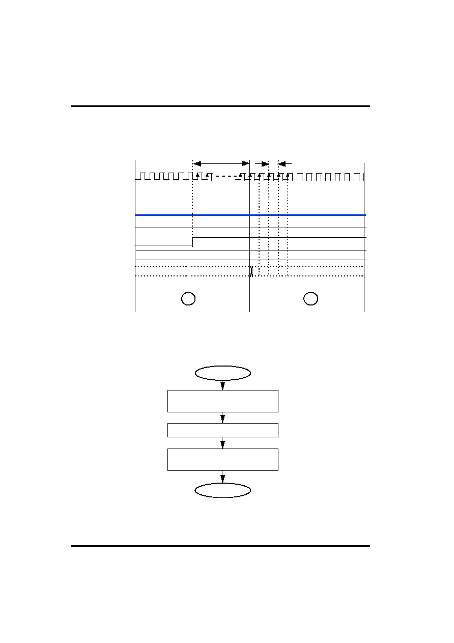
Chapter 4. EPROM
Lock bit read mode (1/2)
Lock bit read mode (2/2)
OSC1
12.5V
Lock Read ( 0101 )
VCC
6V
0V
Lock bit output
1
2
2us at 500KHz
¨ç ¨è
¨õ
¨ô
14.5clocks
START
¨ç
Reset
(Set Lock bit read mode)
¨è
Read Lock bit (D5)
RESETB=0V
VCC=0V
END
4 - 8
Chapter 4. EPROM
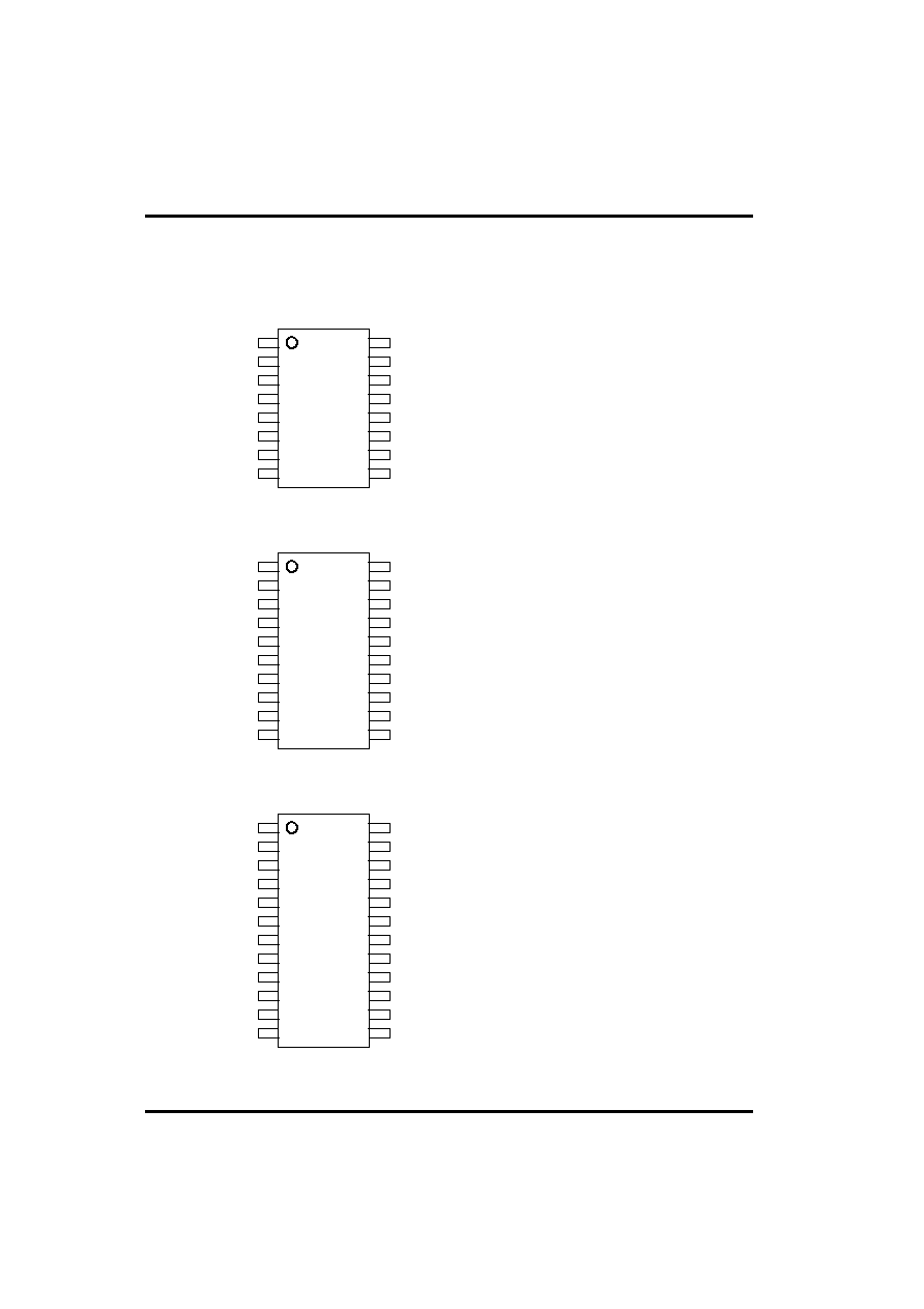
GMS34004T/112T/140T (Pin assignment & Package)
16DIP (Standard TTL DIP Size)
- Width 300mil
- Pin to pin 100mil
20DIP (Standard TTL DIP Size)
- Width 300mil
- Pin to pin 100mil
20SOP (Standard TTL SOP Size)
24DIP (Skinny DIP Size)
- Width 300mil
- Pin to pin 100mil
24SOP (Standard SOP Size)
20 -
19 -
18 -
17 -
16 GND
15 RESETB
14 VDD
13 OSC1
12 -
11 -
K0 1
K1 2
K2 3
K3 4
D0 5
D1 6
D2 7
D3 8
D4 9
D5 10
RESETB 1
GND 2
- 3
- 4
- 5
- 6
K0 7
K1 8
K2 9
K3 10
D0 11
- 12
24 VDD
23 OSC1
22 -
21 -
20 -
19 -
18 D5
17 D4
16 D3
15 D2
14 D1
13 -
16 VDD
15 OSC1
14 -
13 -
12 D5
11 D4
10 D3
9 D2
RESETB 1
GND 2
K0 3
K1 4
K2 5
K3 6
D0 7
D1 8
4 - 9
Chapter 4. EPROM
EPROM(KHz) mode
EPROM write only mode
RESETB
OSC
12.5V
CK1
CK2
CK3
K3 ~ K0
PGM Write ( 0110 )
AH
D4 ~ D0
0000
VCC
6V
0V
1000
1110
AL
DH
DL
10times Repeat
12us X 10 = 120us
5times Repeat
EPROM write
Next Write
1000
0000
1110
AH
AL
DH
DL
2us at 500KHz
¨ç ¨è
¨õ
¨ô
14.5clocks
4 - 10
GMS34004TM / 34112TM / 34140TM
Mode define
Device operation
Execute User pgm
Address in, Data out
Item
User mode
EPROM read mode
EPROM
Program
mode
1Byte PGM Write
2Byte PGM Write
Program verify
Lock bit Write
Lock bit Read
Address in, Data in
Address in, Data in
Address in, Data out
Lock bit write(set D5 to 1)
Lock bit out
Mode setting
RESETB = 0 ~ 3V
Vcc=3V
Vcc=6.0V
Vcc=6.0V
K3~0=0010
K3~0=0110
K3~0=0111
-
K3~0=0100
K3~0=0101
RESETB
=12.5V
RESETB
=12.5V
Lock bit
Program
mode
RESETB
=12.5V
Vcc=6.0V,
Lock bit is D5.
(Default : unlock)
Chapter 4. EPROM
4 - 11
Port define
NMOS open drain I/O
in EPROM mode
* Undefined ports in this table are N.C (No Connection)
Port Name
VDD
RESETB
OSC1
K0
K1
K2
K3
User Mode
3.0V
Reset (0, 3.0V)
Clock input
K0(Input)
K1(Input)
K2(Input)
K3(Input)
EPROM Mode
6.0V
Vpp (0, 12.5V)
Clock input
Read / Write Control
Address / Data Control
D0
D1
D2
D3
D4
D5
D0(Output)
D1(Output)
D2(Output)
D3(Output)
D4(Output)
D5(Output)
A0
A5
Da0
Da4
Lock bit output
GND
0V
A1
A6
Da1
Da5
A2
A7
Da2
Da6
A3
A8
Da3
Da7
A4
A9
-
-
Programming data
Device Name
GMS34004TK
ROM Size
512bytes
Blank data
(HEX)
FF
Lock bit
Yes
Device address
0000 ~ 01FF
File address
0000 ~ 01FF
GMS34112TK
1,024bytes
FF
Yes
0000 ~ 03FF
0000 ~ 03FF
GMS34140TK
1,024bytes
FF
Yes
0000 ~ 03FF
0000 ~ 03FF
- If lock bit is set, the EPROM of the device can not be read, because output is always FF.
- Input file : Intel Hexa format ( *.RHX )
Chapter 4. EPROM

4 - 12
Write / Read data conversion
- You must change MSB ~ LSB
¡ê
LSB ~ MSB.
- Example
Hex
Binary (MSB~LSB)
2C
E4
8D
0010 1100
1110 0100
1000 1101
Write
Read
Hex
Binary (MSB~LSB)
34
27
B1
0011 0100
0010 0111
1011 0001
File / buffer data
Device (D3 ~ D0)
Checksum
- It is calculated from the Buffer of the programmer.
- Address range is the same as device address.
- Calculate mathod is the same as normal EPROM devices (ex:27C128, 256 etc)
Programming control
- OSC1 & RESETB control OTP device, so you must count OSC1 clocks in every state.
- K ports control the internal state of the OTP device(ex: Read, Write...).
- D5~D0 ports are NMOS open drain I/O in EPROM mode.
It must be pulled up by resistors (about 4.7~ 47K ohm).
- The frequency rate of the OSC1 clock is 10KHz ~ 500KHz.
You can hold OSC1 HIGH or LOW state when you need.
Item
Range
VCC
0 ~ 6.0V
¡¾
0.25V
Programming DC specification
RESETB
0 ~ 12.5V
¡¾
0.5V
K-port
D-port
0 ~ 0.2VCC(Low)
0.8VCC ~ VCC (High)
Chapter 4. EPROM
4 - 13
EPROM read mode (1/2)
EPROM read mode (2/2)
RESETB
OSC1
12.5V
For device verify or read.
If you set Lock bit, output data is all 'FF'
D4 ~ D0
K3 ~ K0
A9~A5
A4~A0
D3~D0
D7~D4
ROM Dump Mode ( 0010 )
D5
Port Operation
K Port Latch
High bit
Instruction
Output
Low bit
Instruction
Output
High bit
Address
Latch
Low bit
Address
Latch
Sense
AMP.
Operation
VCC
6V
0V
12Clock
8Clock
Data
Strobe
point
5Clock
Data
Strobe
point
5Clock
Address setting
Data read
Repeat
1
2
3
START
¨ç
Reset
(Set EPROM read mode)
Address=First address
¨è
Set address
¨é
Read data
Address ++
RESETB=0V
VCC=0V
END
Address > Last address
Chapter 4. EPROM
4 - 14
EPROM write mode (1/4)
EPROM write mode (2/4)
RESETB
OSC1
12.5V
K3 ~ K0
PGM Write ( 0110 (1B))
A9~A5
A4~A0
D3~D0
D7~D4
D4 ~ D0
0000
1000
High bit
Instruction
Latch
Low bit
Instruction
Latch
High bit
Address
Latch
Low bit
Address
Latch
K Port Latch
VCC
6V
0V
12Clock
8Clock
1
2
2
First Address Input
First Data Input
RESETB
OSC1
K3 ~ K0
D4 ~ D0
1110
1110
12.5V
1101
Verify
VCC
6V
EPROM write time
3
3
4
Chapter 4. EPROM
4 - 15
EPROM write mode (3/4)
EPROM write mode (4/4)
RESETB
OSC1
K3 ~ K0
D4 ~ D0
1101
12.5V
D3~D0
D7~D4
Verify
A9~A5
A4~A0
D3~D0
D7~D4
0000
1000
High bit
Instruction
Latch
Low bit
Instruction
Latch
High bit
Address
Latch
Low bit
Address
Latch
High bit
Instruction
Output
Low bit
Instruction
Output
Next Address Input
Next Data Input
VCC
6V
Data
Strobe
point
5Clock
Data
Strobe
point
5Clock
4
2
2
No
Fail
Yes
Pass
No
Fail
Pass
Yes
START
¨ç
Reset
(Set EPROM write mode)
Address=First address
¨è
Set address & data
¨é
EPROM write
Repeat until near 100uS.
When 4MHz OSC1, repeat 10
times (12uS*10=120uS)
RESETB=0V
VCC=0V
END
Count=0
Count ++
¨ê
Verify
Count=25?
Device fail
Address ++
¨é
EPROM write
(Write one more time)
Address > Last address
EPROM read mode
Verify all
RESETB=0V
VCC=0V
Device OK
Chapter 4. EPROM
4 - 16
Lock bit write mode (1/3)
Lock bit write mode (2/3)
OSC1
RESETB
12.5V
K3 ~ K0
EPROM Mode Lock Write ( 0100 )
0000
0000
K Port Latch
VCC
6V
0V
12Clock
8Clock
1
2
2
OSC1
1110
1100
12.5V
Write cycle
Repeat 2 times
Lock bit Write
RESETB
K3 ~ K0
VCC
6V
Repeat 10 times
4
3
Chapter 4. EPROM
4 - 17
Lock bit write mode (3/3)
START
¨ç
Reset
(Set Lock bit write mode)
¨è
Wait cycle
¨é
Write cycle *1
Count++
Count=10
RESETB=0V
VCC=0V
END
Count=0
¨ê
Delay cycle
(Repeat 2 times)
Yes
No
*1 Repeat until near 100uS.
When 4MHz OSC1, repeat 10 times
(12uS * 10 = 120uS)
Chapter 4. EPROM
4 - 18
Lock bit read mode (1/2)
Lock bit read mode (2/2)
OSC1
RESETB
12.5V
K3 ~ K0
Lock Read Mode ( 0101 )
1101
1101
K Port Latch
D5
Lock bit output
VCC
6V
0V
You can strobe at any time from here
12Clock
8Clock
1
2
3
START
¨ç
Reset
(Set Lock bit read mode)
¨è
Wait cycle
¨é
Read Lock bit (D5)
RESETB=0V
VCC=0V
END
Chapter 4. EPROM
Document Outline