 | –≠–ª–µ–∫—Ç—Ä–æ–Ω–Ω—ã–π –∫–æ–º–ø–æ–Ω–µ–Ω—Ç: GMS36ser | –°–∫–∞—á–∞—Ç—å:  PDF PDF  ZIP ZIP |

4-BIT SINGLE CHIP MICROCOMPUTERS
GMS36/37XXX(T) SERIES
USER`S MANUAL
∑ GMS36/37004(T)
∑ GMS36/37112(T)
∑ GMS36/37140(T)
JUNE.2001
Rev. 1.1

Revision 1.1
Published by MCU Application Team in HYNIX Semiconductor Inc.
All Right Reserved.
Editor's E-Mail :
rhja@hynix.com
Additional information of this manual may be served by HYNIX Semiconductor Inc.Offices in
Korea or Distributors and Representative listed at address directory.
HYNIX Semiconductor Inc.reserves the right to make changes to any Information here at any
time without notice.
The information, diagrams, and other data in this manual are correct and reliable; however, HYNIX
Semiconductor Inc.is in no way responsible for any violations of patents or other rights of the third
party generated by the use of this manual.

Table of Contents
Chapter 1
GMS36XXX
Description
........................................................1-1
Features
.......................................................1-1
Block diagram
.......................................................1-2
Pin assignment
.......................................................1-3
Pin description
.......................................................1-4
Pin circuit
.......................................................1-5
Port operation
.......................................................1-7
Optional features
.......................................................1-7
Electrical characteristics
.......................................................1-8
Chapter 2
GMS37XXX
Description
........................................................2-1
Features
.......................................................2-1
Block diagram
.......................................................2-2
Pin assignment
.......................................................2-3
Pin description
.......................................................2-4
Pin circuit
.......................................................2-5
Port operation
.......................................................2-7
Optional features
.......................................................2-7
Electrical characteristics
.......................................................2-8
Chapter 3
PACKAGE DIMENSIONS
Chapter 4
FUNCTIONAL DESCRIPTION
Program memory (ROM)
.......................................................4-1
ROM address register
.......................................................4-2
Data memory (RAM)
.......................................................4-3
X-register (X)
.......................................................4-3
Y-register (Y)
.......................................................4-4
Accumulator (Acc)
.......................................................4-4
Arithmetic and Logic Unit (ALU)
.......................................................4-4
State Counter (SC)
.......................................................4-5
Clock generator
.......................................................4-6
Pulse generator
.......................................................4-7
Reset operation
.......................................................4-8
Watch Dog Timer (WDT)
......................................................4-10
Stop operation
......................................................4-11
Table of Contents

Table of Contents
Chapter 5
INSTRUCTION
Instruction format
......................................................5-1
Instruction table
......................................................5-2
Details of instruction system
......................................................5-4
Chapter 6
APPLICATION
Guideline for S/W
......................................................6-1
GMS36112 Circuit diagram
......................................................6-2
GMS37112 Circuit diagram
......................................................6-3
Truth Table for example program ......................................................6-4
Output waveform of uPD6121G ......................................................6-5
Example program-uPD6121G ......................................................6-6
Reference to GMS36XXXT B/D
.....................................................6-12
Reference to GMS37XXXT B/D .....................................................6-13
Chapter 7
GMS36XXXT
Description
........................................................7-1
Features
.......................................................7-1
Pin description
.......................................................7-2
Stop operation
.......................................................7-3
Electrical characteristics
.......................................................7-4
Chapter 8
GMS37XXXT
Description
........................................................8-1
Features
.......................................................8-1
Pin description
.......................................................8-2
Stop operation
.......................................................8-3
Electrical characteristics
.......................................................8-4
Chapter 9
EPROM
Mode define
.......................................................9-1
Port define for GMS36XXXT
.......................................................9-1
Port define for GMS37XXXT
.......................................................9-2
AC/DC timing requirements for program / read mode
...................9-3
Program / verify timing diagrams in kHz version
...................9-4
Program / verify timing diagrams in MHz version
...................9-8
Caution when programming
..................9-14

GMS37XXX
2
PACKAGE DIMENSIONS
3
FUNCTIONAL DESCRIPTION
4
INSTRUCTION
5
GMS36XXX
1
APPLICATION
6
GMS36XXXT
7
GMS37XXXT
8
EPROM
9

1-1
1. GMS36XXX
Description
The GMS36XXX series are remote control transmitter which uses CMOS technology.
This enables transmission code outputs of different configurations, multiple custom code
output, and double push key output for easy fabrication.
The GMS36XXX series are suitable for remote control of TV, VCR, FANS, Air-
conditioners, Audio Equipment, Toys, Games etc.
Features
∑
Program memory
: 1,024 bytes for GMS36004/112/140
∑
Data memory : 32
ÿ
4 bits
∑
43 types of instruction set
∑
3 levels of subroutine nesting
∑
Operating frequency : 300kHz ~ 1MHz at kHz version
2.4MHz ~ 4MHz at MHz version
∑
Instruction cycle :
f
OSC
/6 at kHz version
f
OSC
/48 at MHz version
∑
CMOS process (Single 3.0V power supply)
∑
Stop mode (Through internal instruction)
∑
Released stop mode by key input (Masked option)
∑
Built in Power-on Reset circuit
∑
Built in Low Voltage Detection circuit
∑
Built in capacitor for ceramic oscillation circuit at kHZ version
∑
Built in a watch dog timer (WDT)
∑
Built in transistor for I.R LED Drive : I
OL
=210mA at V
DD
=3V and V
O
=0.3V
∑
Low operating voltage : 2.0 ~ 3.6V (at 300kHz ~ 4MHz)
Chapter 1. GMS36XXX
Series
GMS36004
GMS36112
GMS36140
Program memory
1,024
1,024
1,024
Data memory
32
ÿ
4
I/O ports
-
4
4
Input ports
4
4
4
Output ports
6 (D0~D5)
6 (D0~D5)
10 (D0~D9)
Package
16DIP/SOP
20DIP/SOP/SSOP
24Skinny DIP/SOP
32
ÿ
4
32
ÿ
4
Table 1-1 GMS36XXX series members

1-2
Block Diagram
Fig 1-1 Block Diagram (In case of GMS36140)
RAM
16word x
2page x 4bit
Y-Reg
ACC
ST
R-Latch
X-Reg
MUX
08;
3
6
7
8
11
23
9
10
12
13
14
15
16
17
18
19
20
21
5
4
Instruction
Decoder
Power-on
Reset
Watchdog
timer
24
1
10
10
8
8
4
4
2
4
10
4
10
4
4
4
16
4
4
4
4
4
OSC1 OSC2
K0 ~ K3
R0 ~ R3
D0 ~ D9
REMOUT
VDD GND
OSC
Control Signal
PGND
Low-Voltage
Detection
22
D-Latch
Program counter
3-level
Stack
ROM
64word
ÿ
16page
ÿ
8bit
2
I.R. LED
Drive Tr.
Pulse
Generator
ALU
RAM
Word
Selector
Chapter 1. GMS36XXX

1-3
Pin Assignment
Fig 1-2 GMS36004 Pin Assignment
(16DIP/SOP)
Fig 1-3 GMS36112 Pin Assignment
(20DIP/SOP/SSOP)
Fig 1-4 GMS36140 Pin Assignment
(24Skinny-DIP/SOP)
1
2
3
4
5
6
7
8
16
15
14
13
12
11
10
9
1
2
3
4
5
6
7
8
9
10
20
19
18
17
16
15
14
13
12
11
1
2
3
4
5
6
7
8
9
10
24
23
22
21
20
19
18
17
16
15
11
12
14
13
Chapter 1. GMS36XXX
GND
OSC1
OSC2
K0
K1
K2
K3
D0
VDD
REMOUT
PGND
D5
D4
D3
D2
D1
GND
OSC1
OSC2
K0
K1
K2
K3
R0
R1
R2
VDD
REMOUT
PGND
D5
D4
D3
D2
D1
D0
R3
GND
OSC1
OSC2
K0
K1
K2
K3
R0
VDD
REMOUT
PGND
D5
D4
D3
D2
D1
R1
R2
R3
D9
D8
D0
D6
D7

1-4
Pin
Function
I/O
Connected to 2.0~ 3.6V power supply
Connected to 0V power supply.
K0 ~ K3
Input
GND
-
VDD
-
Each can be set and reset independently.
The output is the structure of N-channel-open-drain.
High current output port driving I.R. LED.
The output is in the form of N-channel-open-drain.
D0 ~ D9
Output
R0 ~ R3
I/O
REMOUT
Output
Oscillator input. Input to the oscillator circuit and connection point for
ceramic resonator.
Internal capacitors available at kHz version.
A feedback resistor is internally connected between this pin and
OSC2.
Connect a resonator between this pin and OSC1.
OSC1
Input
OSC2
Output
High current Tr. ground pin. (connected to GND)
High current output Tr. is connected between this pin and
REMOUT.
PGND
-
Chapter 1. GMS36XXX
Pin Description
4-bit input port with built in pull-up resistor.
STOP mode is released by "L" input of each pin.(masked option)
4-bit I/O port. (Input mode is set only when each of them output "H".)
In outputting, each can be set and reset independently(or at once.)
The output is in the form of C-MOS.
Pull-up resistor and STOP release mode can be respectively selected
as masked option for each pin. (It is released by `'L'' input at STOP.)

1-5
Pin Circuit
Pin
I/O
Note
I/O circuit
- Built in MOS Tr for
pull-up, about 140
œ
.
K0 ~ K3
I
- Open drain output.
- "L" output at reset.
D0 ~ D9
O
- Open drain output.
- Output Tr. disable at
reset.
REMOUT
O
PGND
-
- CMOS output.
- "H" output at reset.
(Option)
- Built in MOS Tr for
pull-up, about 140
œ
.
R0 ~ R3
I/O
REMOUT
PGND
DATA
RESET
pull-up
pull-up
Chapter 1. GMS36XXX

1-6
- Built in feedback-
resistor about 1
–
OSC2
O
Pin
I/O
Note
(Option)
- Built in resonance capacitor
at kHz version
- C1=C2 = 100pF
≤
15%
[C1,C2 are not available
for MHz version]
OSC1
I
I/O circuit
- Built in damping-resistor
[No resistor in MHz operation]
OSC1
STOP
OSC2
C1
C2
Rf
Rd
Chapter 1. GMS36XXX

1-7
Port Operation
Value of X-reg
0 or 1
SO : D(Y)
ý
1 (High-Z)
RO : D(Y)
ý
0
Operation
REMOUT port repeats `'L'' and `'H'' in pulse
frequency. (when PMR = 5, it is fixed at `'L'' )
SO : REMOUT (PMR)
ý
0
RO : REMOUT (PMR)
ý
1 (High-Z)
Value of Y-reg
0 ~ 7
0 or 1
8
0 or 1
SO : D0 ~ D9
ý
1 (High-Z)
RO : D0 ~ D9
ý
0
9
0 or 1
SO : R(Y-Ah)
ý
1
RO : R(Y-Ah)
ý
0
A ~ D
0 or 1
SO : R0 ~ R3
ý
1
RO : R0 ~ R3
ý
0
E
0 or 1
SO : D0 ~ D9
ý
1 (High-Z), R0 ~ R3
ý
1
RO : D0 ~ D9
ý
0,
R0 ~ R3
ý
0
F
2 or 3
SO : D(8)
ý
1 (High-Z)
RO : D(8)
ý
0
0
2 or 3
SO : D(9)
ý
1 (High-Z)
RO : D(9)
ý
0
1
Optional Features
The GMS36XXX series offer the following optional features.
Theses options are masked.
∑
I/O terminals having pull-up resistor : R0 ~ R3
∑
Input terminals having STOP release mode : K0 ~ K3, R0 ~ R3.
∑
Output form at STOP mode
D0 ~ D9 : `'
L'' or keep before stop mode.
Theses options are offered default.
∑
Ceramic oscillation circuit contained (or not contained)
[ This option is not available for MHz Ceramic oscillator. ]
∑
Instruction cycle selection :
T = 48 / f
OSC
or 6 / f
OSC
Chapter 1. GMS36XXX

1-8
Electrical Characteristics
Absolute maximum ratings (Ta = 25
Œ
)
Recommended operating condition
Parameter
Supply Voltage
Power dissipation
Storage temperature range
Input voltage
Output voltage
Unit
V
mW
Œ
V
V
Symbol
V
DD
P
D
Tstg
V
IN
V
OUT
Max. rating
-0.3 ~ 5.0
700 *
-55 ~ 125
-0.3 ~ V
DD
+0.3
-0.3 ~ V
DD
+0.3
* Thermal derating above 25
Œ
: 6mW per degree
Œ
rise in temperature.
Parameter
Supply Voltage
Operating temperature
Symbol
V
DD
Topr
Condition
300KHz ~ 4MHz
-
Rating
2.0 ~ 3.6
-20 ~ +70
Unit
V
Œ
Chapter 1. GMS36XXX

1-9
Electrical characteristics (Ta=25
Œ
, V
DD
= 3V)
*1 Refer to
π
Fig.1-5 I
OL2
vs. V
OL2
Graph
∫
*2 Refer to
π
Fig.1-6 I
OL1
vs. V
OL1
Graph
∫
*3 I
DD1
, I
DD2
, is measured at RESET mode.
Symbol
Limits
Min.
Typ.
Max.
Unit
-
-
1
uA
I
IH
-1
-
-
uA
I
IL
70
140
300
œ
R
PU1
70
140
300
œ
R
PU2
0.3
1.0
3.0
–
R
FD
2.1
-
-
V
V
IH1
-
-
0.9
V
V
IL1
-
0.15
0.4
V
V
OL2
*1
-
0.4
0.9
V
V
OL3
2.1
2.5
-
V
V
OH3
170
210
250
mA
-
-
1
uA
I
OLK1
-
-
1
uA
I
OLK2
-
-
1
uA
I
STP
-
0.2
1.0
mA
I
DD1
*3
-
0.5
1.5
mA
I
DD2
*3
300
-
1000
kHz
f
OSC
2.4
-
4
MHz
f
OSC
I
OL1
*2
f
OSC
/6
f
OSC
/48
Parameter
Input H current
Input L current
K, R Input H voltage
K, R Input L voltage
D, R Output L voltage
OSC2 Output L voltage
OSC2 Output H voltage
REMOUT Output L current
REMOUT leakage current
D, R Output leakage current
Current on STOP mode
Operating Supply current 1
Operating Supply current 2
System
colck
frequency
K Pull-up Resistance
R Pull-up Resistance
Feedback Resistance
Condition
V
I
= V
DD
, R having no Pull-up
V
I
= GND, R having no Pull-up
-
-
I
OL2
= 3mA
I
OL3
= 40uA (kHz) , 150uA(MHz)
I
OH3
= -40uA (kHz), -150uA(MHz)
V
OL1
= 0.3V
V
OUT
= V
DD
, Output off
V
OUT
= V
DD
, Output off
At STOP mode
f
OSC
= 455kHz
f
OSC
= 4MHz
kHz Version
MHz Version.
V
I
= GND
V
I
= GND, Output off
V
OSC1
= GND, V
OSC2
= GND
Chapter 1. GMS36XXX

1-10
[
\[[
][[
^[[
_[[
`[[
a[[
b[[
c[[
d[[
\[[[
[Y[
[Y_
[Yc
\Y]
\Ya
]Y[
]Y_
]Yc
^Y]
^Ya
_Y[
zw\
tz
w
\
l
nnh^Ya
nnh^Y[
nnh]Y[
h ]`
Fig 1-6. I
OL1
vs. V
OL1
Graph. ( REMOUT port)
Fig 1-5. I
OL2
vs. V
OL2
Graph. ( D, R Port )
¥
®µ Œ
™£ Ø™±
£
Ø¡±
™ ™
Chapter 1. GMS36XXX

GMS37XXX
2
PACKAGE DIMENSIONS
3
FUNCTIONAL DESCRIPTION
4
INSTRUCTION
5
GMS36XXX
1
APPLICATION
6
GMS36XXXT
7
GMS37XXXT
8
EPROM
9

2-1
2. GMS37XXX
Description
The GMS37XXX series are remote control transmitter which uses CMOS technology.
This enables transmission code outputs of different configurations, multiple custom code
output, and double push key output for easy fabrication.
The GMS37XXX series are suitable for remote control of TV, VCR, FANS, Air-
conditioners, Audio Equipment, Toys, Games etc.
It is possible to structure the 8 x 7 key matrix for GMS37112, and the 4 x 7 key matrix
for GMS37004.
Features
∑
Program memory
: 1,024 bytes for GMS37004/112/140
∑
Data memory : 32
ÿ
4 bits
∑
43 types of instruction set
∑
3 levels of subroutine nesting
∑
Operating frequency : 300kHz ~ 1MHz at kHz version
2.4MHz ~ 4MHz at MHz version
∑
Instruction cycle :
f
OSC
/6 at kHz version
f
OSC
/48 at MHz version
∑
CMOS process (Single 3.0V power supply)
∑
Stop mode (Through internal instruction)
∑
Released stop mode by key input (Masked option)
∑
Built in Power-on Reset circuit
∑
Built in Low Voltage Detection circuit
∑
Built in capacitor for ceramic oscillation circuit at kHZ version
∑
Built in a watch dog timer (WDT)
∑
Low operating voltage : 2.0 ~ 3.6V (at 300kHz ~ 4MHz)
Chapter 2. GMS37XXX
Table 2-1 GMS37XXX series members
Series
GMS37004
GMS37112
GMS37140
Program memory
1,024
1,024
1,024
Data memory
32
ÿ
4
I/O ports
-
4
4
Input ports
4
4
4
Output ports
7 (D0~D6)
7 (D0~D6)
10 (D0~D9)
Package
16DIP/SOP
20DIP/SOP/SSOP
24Skinny DIP/SOP
32
ÿ
4
32
ÿ
4

2-2
Block Diagram
Fig 2-1 Block Diagram (In case of GMS37140)
RAM
16word x
2page x 4bit
Y-Reg
ACC
ST
R-Latch
X-Reg
MUX
08;
3
6
7
8
11
23
9
10
12
13
14
15
16
17
18
19
20
21
5
4
Instruction
Decoder
Power-on
Reset
Watchdog
timer
24
1
10
10
8
8
4
4
2
4
10
4
10
4
4
4
16
4
4
4
4
4
OSC1 OSC2
K0 ~ K3
R0 ~ R3
D0 D1 D2 D3 D4 D5 D6 D7 D8 D9
REMOUT
VDD GND
OSC
Control Signal
NC
Low-Voltage
Detection
D-Latch
Program counter
3-level
Stack
ROM
64word
ÿ
16page
ÿ
8bit
2
Pulse
Generator
ALU
RAM
Word
Selector
22
* NC : No connection
Chapter 2. GMS37XXX

2-3
Pin Assignment
Fig 2-2 GMS37004 Pin Assignment
(16DIP/SOP)
Fig 2-3 GMS37112 Pin Assignment
(20DIP/SOP/SSOP)
Fig 2-4 GMS37140 Pin Assignment
(24Skinny-DIP/SOP)
1
2
3
4
5
6
7
8
16
15
14
13
12
11
10
9
1
2
3
4
5
6
7
8
9
10
20
19
18
17
16
15
14
13
12
11
1
2
3
4
5
6
7
8
9
10
24
23
22
21
20
19
18
17
16
15
11
12
14
13
Chapter 2. GMS37XXX
GND
OSC1
OSC2
K0
K1
K2
K3/Vpp
D0
VDD
REMOUT
D6
D5
D4
D3
D2
D1
GND
OSC1
OSC2
K0
K1
K2
K3/Vpp
R0
R1
R2
VDD
REMOUT
D6
D5
D4
D3
D2
D1
D0
R3
GND
OSC1
OSC2
K0
K1
K2
K3/Vpp
R0
VDD
REMOUT
NC
D5
D4
D3
D2
D1
R1
R2
R3
D9
D8
D0
D6
D7

2-4
Pin Description
Pin
Function
I/O
Connected to 2.0~ 3.6V power supply
Connected to 0V power supply.
4-bit input port with built in pull-up resistor.
STOP mode is released by "L" input of each pin. ( masked option)
K0 ~ K3
Input
GND
-
VDD
-
Each can be set and reset independently.
The output is the structure of N-channel-open-drain.
4-bit I/O port. (Input mode is set only when each of them output "H".)
In outputting, each can be set and reset independently(or at once.)
The output is in the form of C-MOS.
Pull-up resistor and STOP release mode can be respectively selected
as masked option for each pin. (It is released by "L" input at STOP)
High current output port. The output is in the form of CMOS.
The state of large current on is "H".
D0 ~ D9
Output
R0 ~ R3
I/O
REMOUT
Output
Oscillator input. Input to the oscillator circuit and connection point for
ceramic resonator.
Internal capacitors available at kHz version.
A feedback resistor is internally connected between this pin and OSC2.
Connect a resonator between this pin and OSC1.
OSC1
Input
OSC2
Output
Chapter 2. GMS37XXX

2-5
Pin Circuit
Pin
I/O
Note
I/O circuit
- Built in MOS Tr for
pull-up, about 140
œ
.
K0 ~ K3
I
- Open drain output.
- "L" output at reset.
D0 ~ D9
O
- CMOS output.
- "L" output at reset.
- High current output
source.
REMOUT
O
- CMOS output.
- "H" output at reset.
(Option)
- Built in MOS Tr for
pull-up, about 140
œ
.
R0 ~ R3
I/O
pull-up
pull-up
Chapter 2. GMS37XXX

2-6
- Built in feedback-
resistor about 1
–
OSC2
O
Pin
I/O
Note
(Option)
- Built in resonance capacitor
at kHz version
- C1=C2 = 100pF
≤
15%
[C1,C2 are not available
for MHz version]
OSC1
I
I/O circuit
- Built in damping-resistor
[No resistor in MHz operation]
OSC1
STOP
OSC2
C1
C2
Rf
Rd
Chapter 2. GMS37XXX

2-7
Port operation
Value of X-reg
0 or 1
SO : D(Y)
ý
1 (High-Z)
RO : D(Y)
ý
0
Operation
Value of Y-reg
0 ~ 7
REMOUT port repeats `'H'' and `'L'' in pulse
frequency. (when PMR = 5, it is fixed at `'H'' )
SO : REMOUT (PMR)
ý
1
RO : REMOUT (PMR)
ý
0
0 or 1
8
0 or 1
SO : D0 ~ D9
ý
1 (High-Z)
RO : D0 ~ D9
ý
0
9
0 or 1
SO : R(Y-Ah)
ý
1
RO : R(Y-Ah)
ý
0
A ~ D
0 or 1
SO : R0 ~ R3
ý
1
RO : R0 ~ R3
ý
0
E
0 or 1
SO : D0 ~ D9
ý
1 (High-Z), R0 ~ R3
ý
1
RO : D0 ~ D9
ý
0,
R0 ~ R3
ý
0
F
2 or 3
SO : D(8)
ý
1 (High-Z)
RO : D(8)
ý
0
0
2 or 3
SO : D(9)
ý
1 (High-Z)
RO : D(9)
ý
0
1
Optional Features
The GMS37XXX series offer the following optional features.
Theses options are masked.
∑
I/O terminals having pull-up resistor : R0 ~ R3
∑
Input terminals having STOP release mode : K0 ~ K3, R0 ~ R3.
∑
Output form at STOP mode
D0 ~ D9 :
`'L'' or keep before stop mode.
Theses options are offered default.
∑
Ceramic oscillation circuit contained (or not contained)
[ This option is not available for MHz Ceramic oscillator. ]
∑
Instruction cycle selection :
T = 48 / f
OSC
or 6 / f
OSC
Chapter 2. GMS37XXX

2-8
Electrical Characteristics
Absolute maximum ratings (Ta = 25
Œ
)
Recommended operating condition
Parameter
Supply Voltage
Power dissipation
Storage temperature range
Input voltage
Output voltage
Unit
V
mW
Œ
V
V
Symbol
V
DD
P
D
Tstg
V
IN
V
OUT
Max. rating
-0.3 ~ 5.0
700 *
-55 ~ 125
-0.3 ~ V
DD
+0.3
-0.3 ~ V
DD
+0.3
* Thermal derating above 25
Œ
: 6mW per degree
Œ
rise in temperature.
Parameter
Supply Voltage
Operating temperature
Symbol
V
DD
Topr
Condition
300KHz ~ 4MHz
-
Rating
2.0 ~ 3.6
-20 ~ +70
Unit
V
Œ
Chapter 2. GMS37XXX

2-9
Electrical characteristics (Ta=25
Œ
, V
DD
= 3V)
*1 Refer to
π
Fig.2-5 I
OL2
vs. V
OL2
Graph
∫
*2 Refer to
π
Fig.2-6 I
OL1
vs. V
OL1
Graph
∫
*3 Refer to
π
Fig.2-7 I
OH1
vs. V
OH1
Graph
∫
*4 I
DD1
, I
DD2
, is measured at RESET mode.
Symbol
Limits
Min.
Typ.
Max.
Unit
-
-
1
uA
I
IH
-1
-
-
uA
I
IL
70
140
300
œ
R
PU1
70
140
300
œ
R
PU2
0.3
1.0
3.0
–
R
FD
2.1
-
-
V
V
IH1
-
-
0.9
V
V
IL1
-
0.15
0.4
V
V
OL2
*1
-
0.4
0.9
V
V
OL3
2.1
2.5
-
V
V
OH3
1
2.2
4
mA
-5
-15
-30
mA
-
-
1
uA
I
OLK2
-
-
1
uA
I
STP
-
0.2
1.0
mA
I
DD1
*3
-
0.5
1.5
mA
I
DD2
*3
300
-
1000
kHz
f
OSC
2.4
-
4
MHz
f
OSC
I
OL1
*2
f
OSC
/6
f
OSC
/48
Parameter
Input H current
Input L current
K, R Input H voltage
K, R Input L voltage
D, R Output L voltage
OSC2 Output L voltage
OSC2 Output H voltage
REMOUT Output L current
REMOUT Output H current
D, R Output leakage current
Current on STOP mode
Operating Supply current 1
Operating Supply current 2
System
colck
frequency
K Pull-up Resistance
R Pull-up Resistance
Feedback Resistance
Condition
V
I
= V
DD
, R having no Pull-up
V
I
= GND, R having no Pull-up
-
-
I
OL2
= 3mA
I
OL3
= 40uA (kHz), 150uA (MHz)
I
OH3
= -40uA (kHz), -150uA (MHz)
V
OL1
= 0.4V
V
OH1
= 2V
V
OUT
= V
DD
, Output off
At STOP mode
f
OSC
= 455kHz
f
OSC
= 4MHz
kHz Version
MHz Version.
V
I
= GND
V
I
= GND, Output off
V
OSC1
= GND, V
OSC2
= GND
Chapter 2. GMS37XXX
I
OH1
*3

2-10
[
\
]
^
_
`
a
b
c
[Y[
[Y_
[Yc
\Y]
\Ya
]Y[
]Y_
]Yc
^Y]
^Ya
_Y[
zw\
tz
w
\
l
nnh^Ya
nnh^Y[
nnh]Y[
h ]`
Fig 2-5. I
OL2
vs. V
OL2
Graph. ( D, R Port )
Fig 2-6. I
OL1
vs V
OL1
Graph (REMOUT Port)
¥
®µ Œ
™£ |™}
£
|¡}
™ ™
Chapter 2. GMS37XXX
2-11
X^`
X^[
X]`
X][
X\`
X\[
X`
[
[Y[
[Y_
[Yc
\Y]
\Ya
]Y[
]Y_
]Yc
^Y]
^Ya
_Y[
zs\
t
z
s
\
l
nnh^Ya
nnh^Y[
nnh]Y[
h ]`
Fig 2-7. I
OH1
vs V
OH1
Graph (REMOUT Port)
Chapter 2. GMS37XXX

GMS37XXX
2
PACKAGE DIMENSIONS
3
FUNCTIONAL DESCRIPTION
4
INSTRUCTION
5
GMS36XXX
1
APPLICATION
6
GMS36XXXT
7
GMS37XXXT
8
EPROM
9
3-1
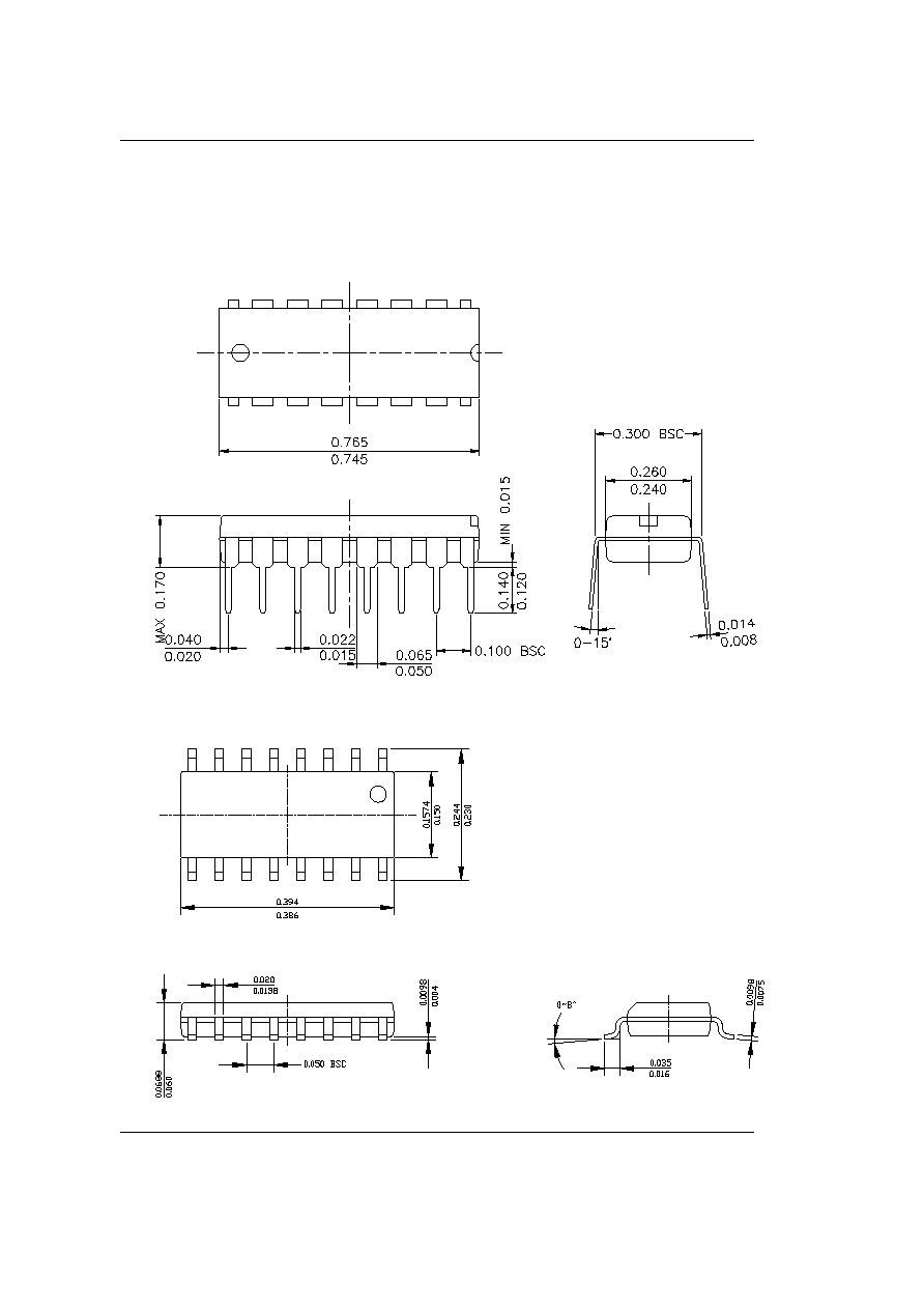
3. PACKAGE DIMENSIONS
The GMS36/37XXX series can be used the following package dimesions.
Fig 3-1. 16PDIP (300MIL)
UNIT : INCH
Fig 3-2. 16SOP (150MIL) (* This type is not supported at OTP)
UNIT : INCH
Chapter 3. PACKAGE DIMENSIONS

3-2
UNIT : INCH
Fig 3-3. 16SOP (300MIL)
Fig 3-4. 20SSOP (150MIL)
UNIT : INCH
Chapter 3. PACKAGE DIMENSIONS

3-3
Fig 3-5. 20PDIP (300MIL)
UNIT : INCH
UNIT : INCH
Fig 3-6. 20SOP (300MIL)
Chapter 3. PACKAGE DIMENSIONS

3-4
Fig 3-7. 24Skinny-DIP (300MIL)
UNIT : INCH
Fig 3-8. 24SOP (300MIL)
UNIT : INCH
Chapter 3. PACKAGE DIMENSIONS

GMS37XXX
2
PACKAGE DIMENSIONS
3
FUNCTIONAL DESCRIPTION
4
INSTRUCTION
5
GMS36XXX
1
APPLICATION
6
GMS36XXXT
7
GMS37XXXT
8
EPROM
9

4-1
4. FUNCTIONAL DESCRIPTION
Program Memory (ROM)
The GMS36/37XXX series can incorporate maximum 1,024 words (64 words
ÿ
16
pages
ÿ
8bits) for program memory. Program counter PC (A0~A5) and page
address register (A6~A9) are used to address the whole area of program memory
having an instruction (8bits) to be next executed.
The program memory consists of 64 words on each page, and thus each page
can hold up to 64 steps of instructions.
The program memory is composed as shown below.
Chapter 4. FUNCTIONAL DESCRIPTION
0 1
2 3
4 5
6 7
8
63
Program counter (PC)
Page address register (PA)
Page buffer (PB)
6
4
(Level "1")
(Level "2")
(Level "3")
(PSR)
(SR)
Stack register
Page 0
Page 1
Page 2
Page 15
A0~A5
0
1
2
15
A6~A9
Program capacity (pages)
Fig 4-1 Configuration of Program Memory
4
6

4-2
ROM Address Register
The following registers are used to address the ROM.
∑ Page address register (PA) :
Holds ROM's page number (0 ~ Fh) to be addressed.
∑ Page buffer register (PB) :
Value of PB is loaded by an LPBI command when newly addressing a page.
Then it is shifted into the PA when rightly executing a branch instruction (BR)
and a subroutine call (CAL).
∑ Program counter (PC) :
Available for addressing word on each page.
∑ Stack register (SR) :
Stores returned-word address in the subroutine call mode.
(1) Page address register and page buffer register :
Address one of pages #0 to #15 in the ROM by the 4-bit binary counter.
Unlike the program counter, the page address register is usually unchanged so
that the program will repeat on the same page unless a page changing command
is issued. To change the page address, take two steps such as (1) writing in the
page buffer what page to jump (execution of LPBI) and (2) execution of BR or CAL,
because instruction code is of eight bits so that page and word can not be specified
at the same time.
In case a return instruction (RTN) is executed within the subroutine that has been
called in the other page, the page address will be changed at the same time.
(2) Program counter :
This 6-bit binary counter increments for each fetch to address a word in the
currently addressed page having an instruction to be next executed.
For easier programming, at turning on the power, the program counter is
reset to the zero location. The PA is also set to "0". Then the program
counter specifies the next ROM address in random sequence.
When BR, CAL or RTN instructions are decoded, the switches on each step
are turned off not to update the address. Then, for BR or CAL, address
data are taken in from the instruction operands (a
0
to a
5
), or for RTN, and
address is fetched from stack register No. 1.
(3) Stack register :
This stack register provides two stages each for the program counter (6bits)
and the page address register (4bits) so that subroutine nesting can be
made on two levels.
Chapter 4. FUNCTIONAL DESCRIPTION

4-3
Data Memory (RAM)
Up to 32 nibbles (16 words
ÿ
2pages
ÿ
4bits) is incorporated for storing data.
The whole data memory area is indirectly specified by a data pointer (X,Y). Page
number is specified by zero bit of X register, and words in the page by 4 bits in
Y-register. Data memory is composed in 16 nibbles/page. Figure 2-2 shows the
configuration.
X-register (X)
X-register is consist of 2bit, X0 is a data pointer of page in the RAM, X1 is only
used for selecting of D8 ~ D9 with value of Y-register
X1=1
X1=0
D8
D9
Y=0
Y=1
D1
D0
Table 4-1 Mapping table between X and Y register
Chapter 4. FUNCTIONAL DESCRIPTION
0
1
2
3
15
Output port
Y-register (Y)
X-register (X)
D0
D9 R0
R3 REMOUT
Page 0
Page 1
0
1
4
a
0
~a
3
Data memory page (0~1)
Fig 4-2 Composition of Data Memory

4-4
Y-register (Y)
Y-register has 4 bits. It operates as a data pointer or a general-purpose register.
Y-register specifies an address (a
0
~a
3
) in a page of data memory, as well as it
is used to specify an output port. Further it is used to specify a mode of carrier
signal outputted from the REMOUT port. It can also be treated as a general-
purpose register on a program.
Accumulator (A
CC
)
The 4-bit register for holding data and calculation results.
Arithmetic and Logic Unit (ALU)
In this unit, 4bits of adder/comparator are connected in parallel as it's main
components and they are combined with status latch and status logic (flag.)
(1) Operation circuit (ALU) :
The adder/comparator serves fundamentally for full addition and data
comparison. It executes subtraction by making a complement by processing
an inversed output of A
CC
(A
CC
+1)
(2) Status logic :
This is to bring an ST, or flag to control the flow of a program. It occurs when
a specified instruction is executed in three cases such as overflow or underflow
in operation and two inputs unequal.
Chapter 4. FUNCTIONAL DESCRIPTION

4-5
State Counter (SC)
A fundamental machine cycle timing chart is shown below. Every instruction is
one byte length. Its execution time is the same. Execution of one instruction
takes 6 clocks for fetch cycle and 6 clocks for execute cycle (12 clocks in total).
Virtually these two cycles proceed simultaneously, and thus it is apparently
completed in 6 clocks (one machine cycle). Exceptionally BR, CAL and RTN
instructions is normal execution time since they change an addressing sequentially.
Therefore, the next instruction is prefetched so that its execution is completed
within the fetch cycle.
Fig. 4-3 Fundamental timing chart
T1 T2 T3 T4 T5 T6 T1 T2 T3 T4 T5 T6
Fetch cycle N
Execute cycle N-1
Execute cycle N
Fetch cycle N-1
Phase
È
Phase
Í
Phase
Î
Machine
Cycle
Machine
Cycle
Chapter 4. FUNCTIONAL DESCRIPTION

4-1
Clock Generator
The GMS36/37XXX series has an internal clock oscillator. The oscillator circuit is
designed to operate with an external ceramic resonator. Internal capacitors are
available at kHz version. Oscillator circuit is able to organize by connecting
ceramic resonator to outside.
* It is necessary to connect capacitor to outside in order to change ceramic resonator,
you must refer to a manufacturer`s resonator matching guide.
Chapter 4. FUNCTIONAL DESCRIPTION
OSC1
OSC2
C1
C2
2
3
rx~^aZ^b\\]v
x}ll
n|
w Y
_]ds•
n~m_]d{
X
n\hn]hz
_^]s•
X
m_^]
n\hn]hz
_``s•
n~m_``p
m_``
n\hn]hz
_c[s•
n~m_c[p
m_c[
n\hn]hz
`[[s•
n~m`[[p
m`[[
n\hn]hz
a_[s•
n~ma_[{
ma_[
n\hn]hz
rx~^aZ^b\\]x
^Ya_xs•
^Yc_xs•
_Y[[xs•
ov
qn}^Ya_x~n`
qn}^Ya_x~n`
qn}_Y[x~n`
vznp}l
vm}X^Ya_xvp
vm}X^Yc_xvp
vm}X_Y[[xvp
x}ll
n~~[^a_xr[a
n~~[^c_xr[a
n~~[_[[xr[^
x}ll
n~nn^Ya_xr[sa
n~nn^Yc_xr[sa
n~nn_Y[[xr
n|
^Ya_xr
^Yc_xr
_Y[[xr
nz}ppns
n}^Ya_x~
n}^Yc_x~
n}_Y[[x~
* All type have the built-in loading capacitors.

4-7
Pulse Generator
The following frequency and duty ratio are selected for carrier signal outputted
from the REMOUT port depending on a PMR (Pulse Mode Register) value set in
a program.
T
T1
* Default value is "0"
* [ ] means the value of "T", when Instruction cycle is f
OSC
/48 in MHz version
Table 4-2 PMR selection table
REMOUT signal
T=1/f
PUL
= 12/f
OSC
[96/f
OSC
], T1/T = 1/2
0
1
PMR
2
3
4
5
T=1/f
PUL
= 12/f
OSC
[96/f
OSC
],
T1/T = 1/3
T=1/f
PUL
= 8/f
OSC
[64/f
OSC
],
T1/T = 1/2
T=1/f
PUL
= 8/f
OSC
[64/f
OSC
],
T1/T = 1/4
T=1/f
PUL
= 11/f
OSC
[88/f
OSC
],
T1/T = 4/11
No Pulse (same to D0 ~ D9)
6
T=1/f
PUL
= 12/f
OSC
[96/f
OSC
],
T1/T = 1/4
7
No pulse (same to D0 ~ D9)
Chapter 4. FUNCTIONAL DESCRIPTION

4-8
Reset Operation
GMS36/37XXX has three reset sources. One is a built-in Power-on reset circuit, another
is a built-in Low VDD Detection circuit, the other is the overflow of Watch Dog Timer. (WDT)
All reset operations are internal in the GMS36/37XXX.
Built-in Power On Reset Circuit
GMS36/37XXX has a built-in Power-on reset circuit consisting of an about 1
–
Resistor
and a 3pF Capacitor. When the Power-on reset pulse occurs, system reset signal is
latched and WDT is cleared. After the overflow time of WDT (2
13
x System clock time)
system reset signal is released.
t
reset
VCC
System
RESETB
About 108msec at
fosc = 455kHz
9''
*1'
&RXQWHU
:'7�
6\VWHP
5(6(7%
–
S)
<GMS36/37XXX>
Fig. 4-4 Power-On Reset Circuit and Timing Chart
Chapter 4. FUNCTIONAL DESCRIPTION

4-9
[Y[
[Y]
[Y_
[Ya
[Yc
\Y[
\Y]
\Y_
\Ya
\Yc
]Y[
]Y]
]Y_
]Ya
]Yc
^Y[
X][
X\[
[
\[
][
^[
_[
`[
a[
b[
ST
ST
w¢ o
xYz n{W }zx
Built-in Low VDD Detection Circuit
GMS36/37XXX has a Low VDD detection circuit.
If VDD become Reset Voltage of Low VDD Detection circuit at active status, system
reset occur and WDT is cleared. After VDD is increased upper Reset Voltage again,
WDT is re-counted and if WDT is overflowed, system reset is released.
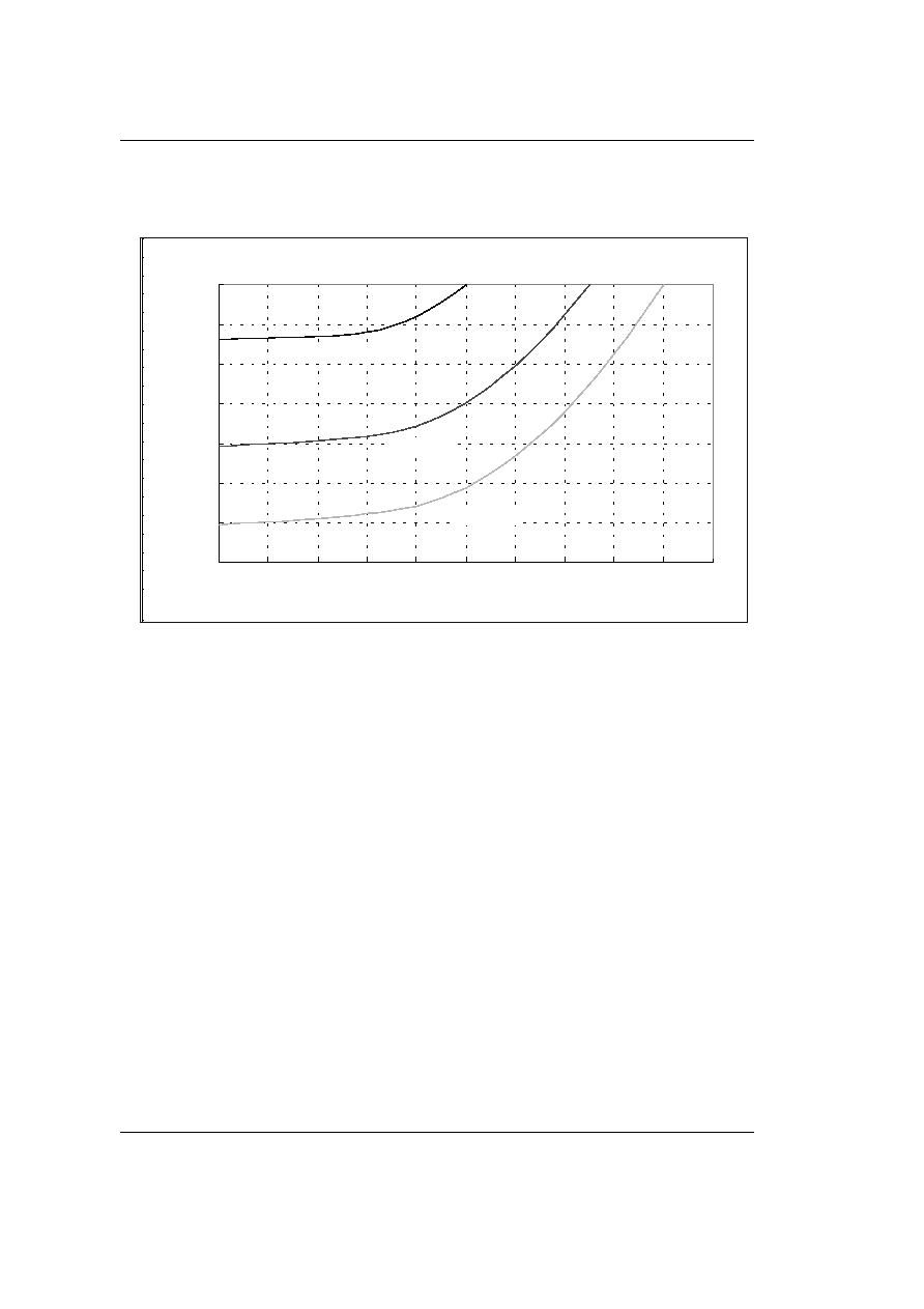
Fig. 4-5 Low Voltage Detection diagram
Fig. 4-6 Low Voltage vs Temperature
VDD
Reset Voltage
Internal
RESETB
About 108msec at fosc =455kHz
Chapter 4. FUNCTIONAL DESCRIPTION

4-10
Watch Dog Timer (WDT)
Watch dog timer is organized binary of 14 steps. The signal of f
OSC
/6 cycle comes
in the first step of WDT after WDT reset. If this counter was overflowed, reset
signal automatically come out so that internal circuit is initialized.
The overflow time is 6
ÿ
2
13
/f
OSC
(108.026ms at f
OSC
=455KHz.)
8
ÿ
6
ÿ
2
13
/f
OSC
(108.026ms at f
OSC
= 3.64MHz)
Normally, the binary counter must be reset before the overflow by using reset
instruction (WDTR), Power-on reset pulse or Low VDD detection pulse.
* It is constantly reset in STOP mode. When STOP is released, counting is
restarted.
f
OSC
/6 or f
OSC
/48
CPU reset
Reset
by instruction
Power-On Reset
Low VDD Detection
Binary counter(14 steps)
RESET (edge-trigger)
Fig. 4-7 Block Diagram of Watch-dog Timer
Chapter 4. FUNCTIONAL DESCRIPTION

4-11
STOP Operation
Stop mode can be achieved by STOP instructions.
In stop mode :
1. Oscillator is stopped, the operating current is low.
2. Watch dog timer is reset, REMOUT output is disable
(High-Z at GMS36XXX(T) , "L" at GMS37XXX(T))
3. Part other than WDT and REMOUT output have a value before
come into stop mode.
* But the state of D0 ~ D9 output in stop mode is able to choose as masked option.
"L" output or same level before come into stop mode.
The Function to release stop mode is able to choose each bit of K or R input as masked option.
Stop mode is released when one of K or R input is going to "L".
1. State of D0 ~ D9 output and REMOUT output is return to state of before stop mode is
achieved.
2. After 2
10
ÿ
{System clock time} for stable oscillating, first instruction start to operate.
3. In return to normal operation, WDT is counted from zero again.
But, at executing stop instruction, if one of K or R input is chosen to "L", stop instruction
is same to NOP instruction.
Chapter 4. FUNCTIONAL DESCRIPTION

GMS37XXX
2
PACKAGE DIMENSIONS
3
FUNCTIONAL DESCRIPTION
4
INSTRUCTION
5
GMS36XXX
1
APPLICATION
6
GMS36XXXT
7
GMS37XXXT
8
EPROM
9

5-1
CHAPTER 5. INSTRUCTION
INSTRUCTION FORMAT
All of the 43 instruction in GMS36/37XXX(T) series is format in two fields of OP
code and operand which consist of eight bits. The following formats are available
with different types of operands.
*Format
È
All eight bits are for OP code without operand.
*Format
Í
Two bits are for operand and six bits for OP code.
Two bits of operand are used for specifying bits of RAM and X-register (bit 1 and
bit 7 are fixed at
Ã
0
Ã
)
*Format
Î
Four bits are for operand and the others are OP code.
Four bits of operand are used for specifying a constant loaded in RAM or Y-
register, a comparison value of compare command, or page addressing in ROM.
*Format
Ï
Six bits are for operand and the others are OP code.
Six bits of operand are used for word addressing in the ROM.
Chapter 5. INSTRUCTION

5-2
INSTRUCTION TABLE
The GMS36/37XXX(T) series provides the following 43 basic instructions.
Category
1
2
3
Register to
Register
LAY
LYA
LAZ
Mnemonic
A
ý
Y
Function
Y
ý
A
A
ý
0
S
S
S
ST
*1
4
5
6
RAM to
Register
LMA
LMAIY
LYM
M(X,Y)
ý
A
M(X,Y)
ý
A, Y
ý
Y+1
Y
ý
M(X,Y)
S
S
S
7
8
LAM
XMA
A
ý
M(X,Y)
A
‰
M(X,Y)
S
S
9
10
11
Immediate
LYI i
LMIIY i
LXI n
Y
ý
i
M(X,Y)
ý
i, Y
ý
Y+1
X
ý
n
S
S
S
12
13
14
RAM Bit
Manipulation
SEM n
REM n
TM n
M(n)
ý
1
M(n)
ý
0
TEST M(n) = 1
S
S
E
15
16
17
ROM
Address
BR a
CAL a
RTN
if ST = 1 then Branch
if ST = 1 then Subroutine call
Return from Subroutine
S
S
S
18
LPBI i
PB
ý
i
S
19
20
21
Arithmetic
AM
SM
IM
A
ý
A + M(X,Y)
A
ý
M(X,Y) - A
A
ý
M(X,Y) + 1
C
B
C
22
23
DM
IA
A
ý
M(X,Y) - 1
A
ý
A + 1
B
S
24
25
IY
DA
Y
ý
Y + 1
A
ý
A - 1
C
B
Chapter 5. INSTRUCTION

5-3
Category
26
27
28
Arithmetic
DY
EORM
NEGA
Mnemonic
Y
ý
Y - 1
Function
A
ý
A + M (X,Y)
A
ý
A + 1
B
S
Z
ST
*1
29
30
Comparison
ALEM
ALEI i
TEST A
ı
M(X,Y)
TEST A
ı
i
E
E
31
32
MNEZ
YNEA
TEST M(X,Y)
Û
0
TEST Y
Û
A
N
N
33
34
YNEI i
KNEZ
TEST Y
Û
i
TEST K
Û
0
N
N
35
RNEZ
TEST R
Û
0
N
36
37
Input /
Output
LAK
LAR
A
ý
K
A
ý
R
S
S
38
39
SO
RO
Output
ý
0 at GMS36XXX, 1 at GMS37XXX
Output
ý
1 at GMS36XXX, 0 at GMS37XXX
S
S
40
41
Control
WDTR
STOP
Watch Dog Timer Reset
Stop operation
S
S
42
43
LPY
NOP
PMR
ý
Y
No operation
S
S
Note) i = 0~f, n = 0~3, a = 6bit PC Address
*1 Column ST indicates conditions for changing status. Symbols have the following
meanings
S : On executing an instruction, status is unconditionally set.
C : Status is only set when carry or borrow has occurred in operation.
B : Status is only set when borrow has not occurred in operation.
E : Status is only set when equality is found in comparison.
N : Status is only set when equality is not found in comparison.
Z : Status is only set when the result is zero.
Chapter 5. INSTRUCTION

5-4
DETAILS OF INSTRUCTION SYSTEM
All 43 basic instructions of the GMS36/37XXX(T) Series are one by one described
in detail below.
Description Form
Each instruction is headlined with its mnemonic symbol according to the
instructions table given earlier.
Then, for quick reference, it is described with basic items as shown below. After
that, detailed comment follows.
∑ Items :
- Naming :
Full spelling of mnemonic symbol
- Status :
Check of status function
- Format :
Categorized into
È
to
Ï
- Operand :
Omitted for Format
È
- Function
Chapter 5. INSTRUCTION

5-5
(1) LAY
Naming :
Load Accumulator from Y-Register
Status :
Set
Format :
I
Function :
A
ý
Y
<Comment>
Data of four bits in the Y-register is unconditionally transferred
to the accumulator. Data in the Y-register is left unchanged.
(2) LYA
Naming :
Load Y-register from Accumulator
Status :
Set
Format :
I
Function :
Y
ý
A
<Comment>
Load Y-register from Accumulator
(3) LAZ
Naming :
Clear Accumulator
Status :
Set
Format :
I
Function :
A
ý
0
<Comment>
Data in the accumulator is unconditionally reset to zero.
(4) LMA
Naming :
Load Memory from Accumulator
Status :
Set
Format :
I
Function :
M(X,Y)
ý
A
<Comment>
Data of four bits from the accumulator is stored in the RAM
location addressed by the X-register and Y-register. Such data
is left unchanged.
(5) LMAIY
Naming :
Load Memory from Accumulator and Increment Y-Register
Status :
Set
Format :
I
Function :
M(X,Y)
ý
A, Y
ý
Y+1
<Comment>
Data of four bits from the accumulator is stored in the RAM
location addressed by the X-register and Y-register. Such data
is left unchanged.
Chapter 5. INSTRUCTION

5-6
(6) LYM
Naming :
Load Y-Register form Memory
Status :
Set
Format :
I
Function :
Y
ý
M(X,Y)
<Comment>
Data from the RAM location addressed by the X-register and
Y-register is loaded into the Y-register. Data in the memory is
left unchanged.
(7) LAM
Naming :
Load Accumulator from Memory
Status :
Set
Format :
I
Function :
A
ý
M(X,Y)
<Comment>
Data from the RAM location addressed by the X-register and
Y-register is loaded into the Y-register. Data in the memory is
left unchanged.
(8) XMA
Naming :
Exchanged Memory and Accumulator
Status :
Set
Format :
I
Function :
M(X,Y)
‰
A
<Comment>
Data from the memory addressed by X-register and Y-register
is exchanged with data from the accumulator. For example,
this instruction is useful to fetch a memory word into the
accumulator for operation and store current data from the
accumulator into the RAM. The accumulator can be restored
by another XMA instruction.
(9) LYI i
Naming :
Load Y-Register from Immediate
Status :
Set
Format :
Î
Operand :
Constant 0
ı
i
ı
15
Function :
Y
ý
i
<Purpose>
To load a constant in Y-register. It is typically used to specify
Y-register in a particular RAM word address, to specify the
address of a selected output line, to set Y-register for
specifying a carrier signal outputted from OUT port, and to
initialize Y-register for loop control. The accumulator can be
restored by another XMA instruction.
<Comment>
Data of four bits from operand of instruction is transferred to
the Y-register.
Chapter 5. INSTRUCTION

5-7
(10) LMIIY i
Naming :
Load Memory from Immediate and Increment Y-Register
Status :
Set
Format :
Î
Operand :
Constant 0
ı
i
ı
15
Function :
M(X,Y)
ý
i, Y
ý
Y + 1
<Comment>
Data of four bits from operand of instruction is stored into the
RAM location addressed by the X-register and Y-register.
Then data in the Y-register is incremented by one.
(11) LXI n
Naming :
Load X-Register from Immediate
Status :
Set
Format :
Í
Operand :
X file address 0
ı
n
ı
3
Function :
X
ý
n
<Comment>
A constant is loaded in X-register. It is used to set X-register in
an index of desired RAM page. Operand of 1 bit of command
is loaded in X-register.
(12) SEM n
Naming :
Set Memory Bit
Status :
Set
Format :
Í
Operand :
Bit address 0
ı
n
ı
3
Function :
M(X,Y,n)
ý
1
<Comment>
Depending on the selection in operand of operand, one of four
bits is set as logic 1 in the RAM memory addressed in
accordance with the data of the X-register and Y-register.
(13) REM n
Naming :
Reset Memory Bit
Status :
Set
Format :
Í
Operand :
Bit address 0
ı
n
ı
3
Function :
M(X,Y,n)
ý
0
<Comment>
Depending on the selection in operand of operand, one of four
bits is set as logic 0 in the RAM memory addressed in
accordance with the data of the X-register and Y-register.
Chapter 5. INSTRUCTION

5-8
(14) TM n
Naming :
Test Memory Bit
Status :
Comparison results to status
Format :
Í
Operand :
Bit address 0
ı
n
ı
3
Function :
M(X,Y,n)
ý
1?
ST
ý
1 when M(X,Y,n)=1, ST
ý
0 when M(X,Y,n)=0
<Purpose>
A test is made to find if the selected memory bit is logic. 1
Status is set depending on the result.
(15) BR a
Naming :
Branch on status 1
Status :
Conditional depending on the status
Format :
Ï
Operand :
Branch address a (Addr)
Function :
When ST =1 , PA
ý
PB, PC
ý
a(Addr)
When ST = 0, PC
ý
PC + 1, ST
ý
1
Note : PC indicates the next address in a fixed sequence that
is actually pseudo-random count.
<Purpose>
For some programs, normal sequential program execution can
be change.
A branch is conditionally implemented depending on the status
of results obtained by executing the previous instruction.
<Comment>
∑ Branch instruction is always conditional depending on the
status.
a. If the status is reset (logic 0), a branch instruction is not
rightly executed but the next instruction of the sequence is
executed.
b. If the status is set (logic 1), a branch instruction is executed
as follows.
∑ Branch is available in two types - short and long. The former
is for addressing in the current page and the latter for
addressing in the other page. Which type of branch to exeute
is decided according to the PB register. To execute a long
branch, data of the PB register should in advance be modified
to a desired page address through the LPBI instruction.
Chapter 5. INSTRUCTION

5-9
(16) CAL a
Naming :
Subroutine Call on status 1
Status :
Conditional depending on the status
Format :
Ï
Operand :
Subroutine code address a(Addr)
Function :
When ST =1 , PC
ý
a(Addr)
PA
ý
PB
SR1
ý
PC + 1,
PSR1
ý
PA
SR2
ý
SR1
PSR2
ý
PSR1
SR3
ý
SR2
PSR3
ý
PSR2
When ST = 0 PC
ý
PC + 1
PB
ý
PS ST
ý
1
Note : PC actually has pseudo-random count against the next
instruction.
<Comment>
∑ In a program, control is allowed to be transferred to a mutual
subroutine. Since a call instruction preserves the return
address, it is possible to call the subroutine from different
locations in a program, and the subroutine can return control
accurately to the address that is preserved by the use of the
call return instruction (RTN).
Such calling is always conditional depending on the status.
a. If the status is reset, call is not executed.
b. If the status is set, call is rightly executed.
The subroutine stack (SR) of three levels enables a subroutine
to be manipulated on three levels. Besides, a long call (to call
another page) can be executed on any level.
∑ For a long call, an LPBI instruction should be executed before
the CAL. When LPBI is omitted (and when PA=PB), a short
call (calling in the same page) is executed.
Chapter 5. INSTRUCTION

5-10
(17) RTN
Naming :
Return from Subroutine
Status :
Set
Format :
È
Function :
PC
ý
SR1
PA, PB
ý
PSR1
SR1
ý
SR2
PSR1
ý
PSR2
SR2
ý
SR3
PSR2
ý
PSR3
SR3
ý
SR3
PSR3
ý
PSR2
ST
ý
1
<Purpose>
Control is returned from the called subroutine to the calling
program.
<Comment>
Control is returned to its home routine by transferring to the PC
the data of the return address that has been saved in the stack
register (SR1).
At the same time, data of the page stack register (PSR1) is
transferred to the PA and PB.
(18) LPBI i
Naming :
Load Page Buffer Register from Immediate
Status :
Set
Format :
Î
Operand :
ROM page address 0
ı
i
ı
15
Function :
PB
ý
i
<Purpose>
A new ROM page address is loaded into the page buffer
register (PB).
This loading is necessary for a long branch or call instruction.
<Comment>
The PB register is loaded together with three bits from 4 bit
operand.
(19) AM
Naming :
Add Accumulator to Memory and Status 1 on Carry
Status :
Carry to status
Format :
È
Function :
A
ý
M(X,Y)+A, ST
ý
1(when total>15),
ST
ý
0 (when total
ı
15)
<Comment>
Data in the memory location addressed by the X and Y-register
is added to data of the accumulator. Results are stored in the
accumulator. Carry data as results is transferred to status.
When the total is more than 15, a carry is caused to put
Ã
1
Ã
in the status. Data in the memory is not changed.
Chapter 5. INSTRUCTION

5-11
(20) SM
Naming :
Subtract Accumulator to Memory and Status 1 Not Borrow
Status :
Carry to status
Format :
È
Function :
A
ý
M(X,Y) - A
ST
ý
1(when A
ı
M(X,Y))
ST
ý
0(when A > M(X,Y))
<Comment>
Data of the accumulator is, through a 2`s complemental
addition, subtracted from the memory word addressed by the
Y-register. Results are stored in the accumulator. If data of
the accumulator is less than or equal to the memory word, the
status is set to indicate that a borrow is not caused.
If more than the memory word, a borrow occurs to reset the
status to
Ã
0
Ã
.
(21) IM
Naming :
Increment Memory and Status 1 on Carry
Status :
Carry to status
Format :
È
Function :
A
ý
M(X,Y) + 1
ST
ý
1(when M(X,Y)
ˆ
15)
ST
ý
0(when M(X,Y) < 15)
<Comment>
Data of the memory addressed by the X and Y-register is
fetched. Adding 1 to this word, results are stored in the
accumulator. Carry data as results is transferred to the status.
When the total is more than 15, the status is set. The memory
is left unchanged.
(22) DM
Naming :
Decrement Memory and Status 1 on Not Borrow
Status :
Carry to status
Format :
È
Function :
A
ý
M(X,Y) - 1
ST
ý
1(when M(X,Y)
ˆ
1)
ST
ý
0 (when M(X,Y) = 0)
<Comment>
Data of the memory addressed by the X and Y-register is
fetched, and one is subtracted from this word (addition of Fh)>
Results are stored in the accumulator. Carry data as results is
transferred to the status. If the data is more than or equal to
one, the status is set to indicate that no borrow is caused. The
memory is left unchanged.
Chapter 5. INSTRUCTION

5-12
(23) IA
Naming :
Increment Accumulator
Status :
Set
Format :
È
Function :
A
ý
A+1
<Comment>
Data of the accumulator is incremented by one. Results are
returned to the accumulator.
A carry is not allowed to have effect upon the status.
(24) IY
Naming :
Increment Y-Register and Status 1 on Carry
Status :
Carry to status
Format :
È
Function :
Y
ý
Y + 1
ST
ý
1 (when Y = 15)
ST
ý
0 (when Y < 15)
<Comment>
Data of the Y-register is incremented by one and results are
returned to the Y-register.
Carry data as results is transferred to the status. When the
total is more than 15, the status is set.
(25) DA
Naming :
Decrement Accumulator and Status 1 on Borrow
Status :
Carry to status
Format :
È
Function :
A
ý
A - 1
ST
ý
1(when A
ˆ
1)
ST
ý
0 (when A = 0)
<Comment>
Data of the accumulator is decremented by one. As a result
(by addition of Fh), if a borrow is caused, the status is reset to
Ã
0
Ã
by logic. If the data is more than one, no borrow occurs
and thus the status is set to
Ã
1
Ã
.
Chapter 5. INSTRUCTION

5-13
(26) DY
Naming :
Decrement Y-Register and Status 1 on Not Borrow
Status :
Carry to status
Format :
È
Function :
Y
ý
Y -1
ST
ý
1 (when Y
ˆ
1)
ST
ý
0 (when Y = 0)
<Purpose>
Data of the Y-register is decremented by one.
<Comment>
Data of the Y-register is decremented by one by addition of
minus 1 (Fh).
Carry data as results is transferred to the status. When the
results is equal to 15, the status is set to indicate that no
borrow has not occurred.
(27) EORM
Naming :
Exclusive or Memory and Accumulator
Status :
Set
Format :
È
Function :
A
ý
M(X,Y) + A
<Comment>
Data of the accumulator is, through a Exclusive OR,
subtracted from the memory word addressed by X and Y-
register. Results are stored into the accumulator.
(28) NEGA
Naming :
Negate Accumulator and Status 1 on Zero
Status :
Carry to status
Format :
È
Function :
A
ý
A + 1
ST
ý
1(when A = 0)
ST
ý
0 (when A != 0)
<Purpose>
The 2`s complement of a word in the accumulator is obtained.
<Comment>
The 2`s complement in the accumulator is calculated by adding
one to the 1`s complement in the accumulator. Results are
stored into the accumulator. Carry data is transferred to the
status. When data of the accumulator is zero, a carry is
caused to set the status to
Ã
1
Ã
.
Chapter 5. INSTRUCTION

5-14
(29) ALEM
Naming :
Accumulator Less Equal Memory
Status :
Carry to status
Format :
È
Function :
A
ı
M(X,Y)
ST
ý
1 (when A
ı
M(X,Y))
ST
ý
0 (when A > M(X,Y))
<Comment>
Data of the accumulator is, through a complemental addition,
subtracted from data in the memory location addressed by the
X and Y-register. Carry data obtained is transferred to the
status. When the status is
Ã
1
Ã
, it indicates that the data of
the accumulator is less than or equal to the data of the
memory word. Neither of those data is not changed.
(30) ALEI
Naming :
Accumulator Less Equal Immediate
Status :
Carry to status
Format :
Î
Function :
A
ı
i
ST
ý
1 (when A
ı
i)
ST
ý
0 (when A > i)
<Purpose>
Data of the accumulator and the constant are arithmetically
compared.
<Comment>
Data of the accumulator is, through a complemental addition,
subtracted from the constant that exists in 4bit operand. Carry
data obtained is transferred to the status. The status is set
when the accumulator value is less than or equal to the
constant. Data of the accumulator is left unchanged.
(31) MNEZ
Naming :
Memory Not Equal Zero
Status :
Comparison results to status
Format :
È
Function :
M(X,Y)
Û
0
ST
ý
1(when M(X,Y)
Û
0)
ST
ý
0 (when M(X,Y) = 0)
<Purpose>
A memory word is compared with zero.
<Comment>
Data in the memory addressed by the X and Y-register is
logically compared with zero. Comparison data is thransferred
to the status. Unless it is zero, the status is set.
Chapter 5. INSTRUCTION

5-15
(32) YNEA
Naming :
Y-Register Not Equal Accumulator
Status :
Comparison results to status
Format :
È
Function :
Y
Û
A
ST
ý
1 (when Y
Û
A)
ST
ý
0 (when Y = A)
<Purpose>
Data of Y-register and accumulator are compared to check if
they are not equal.
<Comment>
Data of the Y-register and accumulator are logically compared.
Results are transferred to the status. Unless they are equal,
the status is set.
(33) YNEI
Naming :
Y-Register Not Equal Immediate
Status :
Comparison results to status
Format :
Î
Operand :
Constant 0
ı
i
ı
15
Function :
Y
Û
i
ST
ý
1 (when Y
Û
i)
ST
ý
0 (when Y = i)
<Comment>
The constant of the Y-register is logically compared with 4bit
operand. Results are transferred to the status. Unless the
operand is equal to the constant, the status is set.
(34) KNEZ
Naming :
K Not Equal Zero
Status :
The status is set only when not equal
Format :
È
Function :
When K
Û
0, ST
ý
1
<Purpose>
A test is made to check if K is not zero.
<Comment>
Data on K are compared with zero. Results are transferred to
the status. For input data not equal to zero, the status is set.
(35) RNEZ
Naming :
R Not Equal Zero
Status :
The status is set only when not equal
Format :
È
Function :
When R
Û
0, ST
ý
1
<Purpose>
A test is made to check if R is not zero.
<Comment>
Data on R are compared with zero. Results are transferred to
the status. For input data not equal to zero, the status is set.
Chapter 5. INSTRUCTION

5-16
(36) LAK
Naming :
Load Accumulator from K
Status :
Set
Format :
È
Function :
A
ý
K
<Comment>
Data on K are transferred to the accumulator
(37) LAR
Naming :
Load Accumulator from R
Status :
Set
Format :
È
Function :
A
ý
R
<Comment>
Data on R are transferred to the accumulator
(38) SO
Naming :
Set Output Register Latch
Status :
Set
Format :
È
Function :
D(Y)
ý
1
0
ı
Y
ı
7
REMOUT
ý
0(PMR=5)
Y = 8 at GMS36XXX(T)
REMOUT
ý
1(PMR=5)
Y = 8 at GMS37XXX(T)
D0~D9
ý
1 (High-Z)
Y = 9
R(Y)
ý
1
Ah
ı
Y
ı
Dh
R
ý
1
Y = Eh
D0~D9, R
ý
1
Y = Fh
<Purpose>
A single D output line is set to logic 1, if data of Y-register is
between 0 to 7.
Carrier frequency come out from REMOUT port, if data of
Y-register is 8.
All D output line is set to logic 1, if data of Y-register is 9.
It is no operation, if data of Y-register between 10 to 15.
When Y is between Ah and Dh, one of R output lines is set at
logic 1.
When Y is Eh, the output of R is set at logic 1.
When Y is Fh, the output D0~D9 and R are set at logic 1.
<Comment>
Data of Y-register is between 0 to 7, selects appropriate D
output.
Data of Y-register is 8, selects REMOUT port.
Data of Y-register is 9, selects all D port.
Data in Y-register, when between Ah and Dh, selects an
appropriate R output (R0~R3).
Data in Y-register, when it is Eh, selects all of R0~R3.
Data in Y-register, when it is Fh, selects all of D0~D9 and
R0~R3.
Chapter 5. INSTRUCTION

5-17
(39) RO
Naming :
Reset Output Register Latch
Status :
Set
Format :
È
Function :
D(Y)
ý
0
0
ı
Y
ı
7
REMOUT
ý
1
Y = 8 at GMS36XXX(T)
REMOUT
ý
0
Y = 8 at GMS37XXX(T)
D0~D9
ý
0
Y = 9
R(Y)
ý
0
Ah
ı
Y
ı
Dh
R
ý
0
Y = Eh
D0~D9, R
ý
0
Y = Fh
<Purpose>
A single D output line is set to logic 0, if data of Y-register is
between 0 to 9.
REMOUT port is set to logic 0, if data of Y-register is 9.
All D output line is set to logic 0, if data of Y-register is 9.
When Y is between Ah and Dh, one of R output lines is set at
logic 0.
When Y is Eh, the output of R is set at logic 0
When Y is Fh, the output D0~D9 and R are set at logic 1.
<Comment>
Data of Y-register is between 0 to 7, selects appropriate D
output.
Data of Y-register is 8, selects REMOUT port.
Data of Y-register is 9, selects D port.
Data in Y-register, when between Ah and Dh, selects an
appropriate R output (R0~R3).
Data in Y-register, when it is Eh, selects all of R0~R3.
Data in Y-register, when it is Fh, selects all of D0~D9 and
R0~R3.
(40) WDTR
Naming :
Watch Dog Timer Reset
Status :
Set
Format :
È
Function :
Reset Watch Dog Timer (WDT)
<Purpose>
Normally, you should reset this counter before overflowed
counter for dc watch dog timer. this instruction controls this
reset signal.
Chapter 5. INSTRUCTION

5-18
(41) STOP
Naming :
STOP
Status :
Set
Format :
È
Function :
Operate the stop function
<Purpose>
Stopped oscillator, and little current.
(See 1-12 page, STOP function.)
(42) LPY
Naming :
Pulse Mode Set
Status :
Set
Format :
È
Function :
PMR
ý
Y
<Comment>
Selects a pulse signal outputted from REMOUT port.
(43) NOP
Naming :
No Operation
Status :
Set
Format :
È
Function :
No operation
Chapter 5. INSTRUCTION

GMS37XXX
2
PACKAGE DIMENSIONS
3
FUNCTIONAL DESCRIPTION
4
INSTRUCTION
5
GMS36XXX
1
APPLICATION
6
GMS36XXXT
7
GMS37XXXT
8
EPROM
9

6-1
Guideline for S/W
1. All rams need to be initialized to zero in reset address for proper design.
2. Make the output ports `H` after reset.
3. Do not use WDTR instruction in subroutine.
4. Before reading the input port the waiting time should be more than 200uS.
5. To decrease current consumption, make the output port as high in normal routine except
for key scan strobe and STOP mode.
6. We recommend you do not use all 64 bytes in a page. You had better write ` BR $` in
unused area. This will help you prevent unusual operation of MCU.
7. Be careful not to use long call or branch (CALL,BL) with arithmetic manipulation.
If you want to use branch right after arithmetic manipulation, the long call or branch will be
against your intention.
ex) LAR ; The value of R ports -> Accumulator
ALEI 14 ; A
ı
14 : S = 1, A
14 : S = 0
BL TRUE ; S is always 1 because BL is composed of LPBI and BR.
-------------- Fail
LAR ; The value of R ports -> Accumulator
ALEI 14 ; A
ı
14 : S = 1, A
14 : S = 0
BR TRUE ; When S is 1 Branch will occur. Otherwise Branch will not occur and
LAK
; next instruction will be operated.
-------------- Right
Chapter 6. Application

6-2
.
.
.
.
5
5
5
5
'
'
'
'
'
'
9GG
5(0
287
26&
26&
*
06
5%
;;;
*06 &LUFXLW 'LDJUDP
*1'
3*1'
We recommend
alkaline battery
Chapter 6. Application

6-3
.
.
.
.
5
5
5
5
'
'
'
'
'
'
'
9GG
5(0
287
26&
26&
*
06
5&;
;;
*06 &LUFXLW 'LDJUDP
*1'
We recommend
alkaline battery
Chapter 6. Application

6-4
7UXWK 7DEOH IRU H[DPSOH SURJUDP
vp yzY
ollSsT
vp yzY
ollSsT
v[\
[[
v]d
\n
v[]
[\
v^[
\o
v[^
[]
v^\
\p
v[_
[^
v^]
\q
v[`
[_
v^^
][
v[a
[`
v^_
]\
v[b
[a
v^`
]]
v[c
[b
v^a
]^
v[d
[c
v^b
]_
v\[
[d
v^c
]`
v\\
[l
v^d
]a
v\]
[m
v_[
]b
v\^
[n
v_\
]c
v\_
[o
v_]
]d
v\`
[p
v_^
]l
v\a
[q
v__
]m
v\b
\[
v_`
]n
v\c
\\
v_a
]o
v\d
\]
v_b
]p
v][
\^
v_c
]q
v]\
\_
v_d
^[
v]]
\`
v`[
^\
v]^
\a
v`\
^]
v]_
\b
v`]
^^
v]`
\c
v`^
^_
v]a
\d
v`_
^`
v]b
\l
v``
^a
v]c
\m
v`a
^b
CUSTOM:04H
Chapter 6. Application

6-5
7F
7
&DUULHU IUHTXHQF\
I
&$5
7F I
26&
'XW\ UDWLR 77F
2XWSXW ZDYHIRUP RI X3'*
$ VLQJOH SXOVH PRGXODWHG ZLWK .+] VLJQDO DW .+]
- Configuration of Flame
1st flame
C0 C1 C2 C3 C4 C5 C6 C7 C0 C1 C2 C3 C4 C5 C6 C7 D0 D1 D2 D3 D4 D5 D6 D7 D0 D1 D2 D3 D4 D5 D5 D7
Lead code
Custom code
Custom code
Data code
Data code
9ms
4.5ms
- Bit Description
- Flame Interval : Tf
The transmitted waveform as long as a key is depressed
0.56ms
1.125ms
0.56ms
2.25ms
Bit
Ã
0
Ã
Bit
Ã
1
Ã
Tf=108mS
Tf=108mS
- Repeat code
9ms
2.25ms
0.56ms
Chapter 6. Application

6-6
¢ © ° ß
® º Ω « ƒ ∆ √ ª ∆ µ ¡ Ω « π Ã µ ¡ ƒ ¿ π ƒ ∆ √ ª ∆ µ ¡ ∫ √ ∆ ° ß π π Ω ¬ ¶ ©
® º π ∫ √ ∆ ¡ µ » Ω « ¢ ∫ √ ∆ ¡ µ »
¶ ° ¢
¨
£ © ¢ ®
• ©
¢ £ ¢
• ©
® ¢
¶ ß ®
• ©
¶ § ®
• ©
¢ ®
• ©
® £ ®
• ©
§ £ ¢ ®
• ©
ß ® ¶ £
• ©
• ©
• ©
• ©
• ©
¢ ´ ®
• ©
¢ ´ ®
• ©
®
• ©
®
• ©
£
• ©
£
• ©
§
¶ ß ®
¨
¶ ° ¶
°
¢
¶
t t ß £
t t t t t t t t t t t t t t t t t
t t ° t ß ® ¶ £ t § £ ¶ ® t £ ´ t £ ¶ t ß ® £ § t ° £
® £ ¶ £ t t t t t t ¶ £
t t t t t t t t t t
t t t t t t t t t t ¶ t t t t t t t t ® £ ¶ £
t t t t t t t t t t t t t t t t ® ° t
t t £ ¶ t ß ® Æ ® £ ¢ t § £ ¶ ®
t t t t t t t t t t ß ® £ §
t t t t t t t t t t t
° ¢ t t t t t t ¨ t t t t t t t
t t t t t t t t t t t t t t t t t
t § £ ¶ ® t t £ ¶ t ¶ ß ¢ t © ¶ ¶ ¢ ® t £ ¢ ß © ° § ® £ ¢
t t t t t t t t t t ß £
t t t t t t t t t t t t t t t t t £ © ¢ ®
t t t t t t t t t t °
t t t t t
t t t t t t t t t t t t t t t
t t t t t t t t t t §
t t t t t t t t t t t t t t t t t £ © ¢ ®
t t t t t t t t t t ¶ ° t t t t t t t ¶ ß ®
t t t t t t t t t t ¶ ° t t t t t t t ¢ £ ¢
ß ¢ t t t t t t t t t t t t t ¢ ®
t t t t t t t t t t ° t t t t t
¶ t t t t t t t ° t t t t t
t t t t t t t t t t ¢ t t t t t t ®
t t t t t t t t t t ¶ t t t t t t t t ¶
t t t t t t t t t t t t t t t t ß ¢
t t t t t t t t t t ´ ® ¶
t £ ¢ { ® t © ß t ´ ® ¶ t ¢ t ß © ¶ £ © ® ¢
t t t t t t t t t t t t t t t t t ® £ ®
t t t t t t t t t t ° ¢ Æ
t t t t t t t t t t ¶ t t t t t t t t
t t t t t t t t t t t t t t t t t £ © ¢ ®
t t t t t t t t t t ® ° t t t t t t t t ¢ £ ¢
t t t t t t t t t t ¶ t t t t t t t t ¶ ß ®
t t t t t t t t t t ß ° t t t t t t t ¢ £ ¢
t t t t t t t t t t ¶ t t t t t t t t ß ¢
t t t t t °
t t t t t t t t t t ¢ t t t t t t
t t t t t t t t t t ¶ t t t t t t t t ° ¢
% /
. ( <
Example program - uPD6121G
Chapter 6. Application

6-7
® £ ° t t t t t t t t t t t t £ ° § ¶
t t t t t t t t t t t t t t t t
t t t t t t t t t t ¶ t t t t t t t t ® £ °
t t t t t t t t t t t t t t t t t t ® °
® £ ° t t t t
t t t t t t t t t t t t t t t t t £ ° § ¶
t t t t t t t t t t t t t t t t
t t t t t t t t t t ¶ t t t t t t t t ®
t t t t t t t t t t ¶ t t t t t t t t ¶ ¶ ® ¢
® t t t t t t t t t t t t
t t t t t t t t t t ¶ ® ¢
£ ° § ¶ t t °
t t t t t t t t t t
t t t t t t t t t t
t t t t t t t t t t £ ¶ °
¶ ¶ ® ¢ t t t t t t ¶ ® ¢
t t t t t
t t t t t t t t t t t
t t t t t t t t t t ¢ £ §
t t ¶ t t t t t t t t x
t ¢ t ¶ ß ß
t t t t t t t t t t § t t t t t t t t
t t t t t t t t t t ¶ t t t t t t t t x
ß ® ¶ ® t ¶ ß ß
ß ¢ t t t t t t t t t t t t § £ ¢ ®
t t t t t t t t t t °
t t t t t t t t t t ¶ £
t t t t t t t t t t t t t t t t ® ° t
t £ ¶ t t ß ¢
t t t t t t t t t t
t t t t t t t t t t t t t t t t
t t t t t t t t t t t t t t t t t ß ™
t t t t t t t t t t ¶
t t t t t t t t t t t t t t t t
t t t t t t t t t t t t t t t t t ¶ ß ™
t t t t t t t t t t t t t t t t t
t t t t t t t t t t ß £
§ £ ¢ ®
°
°
¶
ß ¢
¶ ® ¢
ß ™
¢ £ §
¶
ß ™
¶ ß ™
¢ ´ ®
ß °
ß ™
¢ ®
°
°
°
°
ß ® ¶ £
°
¶ ® ¢
£ © ¢
£ © ¢ ®
® °
¶ ß ®
¶
ß °
¶ ß ®
¢ ´ ®
® ° £ ™
°
ß ¢
¢ ´ ®
® £ °
¢
¶
Chapter 6. Application

6-8
t t t t t t t t t t t t t t t t t ®
t t t t t t t t t t t t t t t t ® £ °
t t t t t t t t t t ¢ t t t t t t
t t t t t t t t t t ¶ t t t t t t t t
t t t t t t t t t t t t ®
t t t t t t t t t t t t t t t t ® ° £ ™
t t t t t t t t t t t t t t t t t t © ß ¶
t t t t t t t t t t t t £ © ¢ ®
t t t t t t t t t t ¶ ° t t t t t t t ¶ § ®
t t t t t t t t t t ¶ t t t t t t t t
t t t t t t t t t t t
t t t t t t t t t t ¢ £ §
t t t t t t t t t t ¶
t t t t x
t t t t t t t t t t § t t t t t t t t
t t t t t t t t t t ¶ t t t t t t t t x
t t t t t t t t t t t t ß ® ¶ £
t t t t t t t t t t ® ° t t t t t t t t
t t t t t t t t t t ¶ t t t t t t t t £ £ §
t t t t t t t t t t ¢ £ §
t t t t t t t t t t ¶ t t t t t t t t £ £ §
£ £ § t t t t t t t t t t t t ¢ ´ ®
t t t t t t t t t t ß ° t t t t t t t
£ £ § t t t t t t t t t t t t ß ® ¶ £
t t t t t t t t t t °
t t t t t t t t t t t t t t t t t ¢ ´ ®
t t t t t t t t t t t
t t t t t t t t t t t t t t t t
t t t t t t t t t t ¶ t t t t t t t t ¢ ®
t t t t t t t t t t t t t t t t
t t t t t t t t t t ¶ t t t t t t t t ¢ ®
t t t t t t t t t t t t t t t t
t t t t t t t t t t ¶ t t t t t t t t ¢ ®
t t t t t t t t t t ° t t t t t
t t ¶ t t t t t t t t ¢ ™
¢ ® t t t t t t t ° t t t t t
t t t t t t t t t t t t t t t t ® °
t t t t t t t t t t ¶ t t t t t t t t ¢ ™
¢ ® t t t t t t t ° t t t t t
t t t t t t t t t t ¢ £ §
t t t t t t t t t t ¢ £ §
t t t t t t t t t t ¶ t t t t t t t t ¢ ™
¢ ® t t t t t t t ° t t t t t
t t t t t t t t t t ¢ £ §
t t t t t t t t t t t t t t t t t t t t t t
¢ ™ t t t t t t t t t t t t t ¢ ®
t t t t t t t t t t °
t t t t t t t t t t t t t t t t t
t t t t t t t t t t t t t t t t
t t t t t t t t t t ¶ t t t t t t t t ´
t t t t t t t t t t t t t t t t
t t t t t t t t t t ¶ t t t t t t t t £ ¢ t t t t t t
t t t t t t t t t t t t t t t t
t t t t t t t t t t ¶ t t t t t t t t ´
t t t t t t t t t t t t t t t t
t t t t t t t t t t ¶ t t t t t t t t £ ¢ t t t t t t
t t t t t t t t t t t t t t t t
t t t t t t t t t t ¶ t t t t t t t t ´
t t t t t t t t t t t t t t t t
t t t t t t t t t t ¶ t t t t t t t t £ ¢ t t t t t t
t t t t t t t t t t t t t t t t
t t t t t t t t t t ¶ t t t t t t t t £ ¢ ™ t t t t t t
´ t t t t t t t t t t t t t ° ¢
£ ¢ t t t t t t
t t t t t t t t t t t t t t t t ® °
£ ¢ t t t t t t
t t t t t t t t t t t t t t t t ® °
Chapter 6. Application

6-9
£ ¢ t t t t t t
t t t t t t t t t t ¢ £ §
£ ¢ ™ t t t t t t
t t t t t t t t t t t t t t t t t ¢ ´ ®
t t t t t t t t t t °
t t t t t t t t t t °
t t t t t t t t t t t t t t t t t t £ © ¢
t t t
t t t
t t ¢ £ §
t t t t t t t t t t ¶ t t t t t t t t x
t t t t t t t t t t § t t t t t t t t
t t t t t t t t t t ¶ t t t t t t t t x
© ß ¶ t t t t t t t t t t
t t t t t t t t t t ° t t t t t
t t t t t t t t t t ° t t t t t
t t t t t t t t t t ° t t t t t
t t t t t t t t t t ° t t t t t
© ß £ ° t t t t t t t t t t t ¢ ´ ®
t t t t t t t t t t t t t t t t ¶ t t t t t t t t ¢ ´ ®
t t t t t t t t t t t t t t t t t
t t t t t t t t t t ß £ t t t t t t t t t t t t t t t t t t t
t t t t t t t t t t t t t t t t t
t t t t t t t t t t t t t t t t °
t t t t t t t t t t t t t t t t ® °
t t t t t t t t t t t t t t t t t
t t t t t t t t t t ¶ £ t t t t t t t t t t t t t t t t t t t t ¶ £
t t t t t t t t t t t t t t t t t
t t t t t t t t t t t t t t t t °
t t t t t t t t t t t t t t t t ® °
t t t t t t t t t t t t t t t t t £ © ¢ ®
t t t t t t t t t t ® ° t t t t t t t t ¶ § ®
t t t t t t t t t t ¶ t t t t t t t t
© £ t t t t t t t t t t t
t t t t t t t t t t t t t t t t °
t t t t t t t t t t t t t t t t ® °
t t t t t t t t t t t t t t t t t § £ ¢ ®
t t t t t t t t t t ° t t t t t
t t t t t t t t t t t t t t t t t t ® ¨
t t t t t t t t t t t t t § © ß
t t t t t t t t t t t t t t t t t
t t t t t t t t t t t t t t t t t °
t t
t t t t °
t t t t t t t t t t t t t t t t t °
t t t t t t t t t t ´ ® ¶
t t t t t t t t t t t t t t t t t °
t t t t t t t t t t t t t t t t t °
t t t t t t t t t t t t t t t t ® °
t t t t t t t t t t t t t t t t t t
° t t t t t t t t t t ® °
° t t t
t t t t t t t t t t ¶ t t t t t t t t °
t t t t t t t t t t ¶ ® ¢
t t t t t t t t t t t
t t t
t t
© ¢ © ß t ¢ ß ® ¶ © ® £ ¢ t ß t ´ ¶ ® ® ¢ t ¢ t ¢ t ¶
t t t
t t
t t t
t t
t t t
t t
t t t t t t t t t t Æ
t t t t t t t t t t ¨ °
t t t t t t t t t t ¢ Æ
t t t t t t t t t t ¶ ¢ Æ
t t t t t t t t t t °
t t t t t t t t t t ¢ £ §
t t t t t t t t t t
t t t t t t t t t t ¶ t t t t t t t t x
t t t t t t t t t t § t t t t t t t t
Chapter 6. Application

6-10
t t t t t t t t t t ¶ t t t t t t t t x
§ © ß t t t t t t t t t t t ® °
§ © ß t t t t t t t t t t t
t t t t t t t t t t ß £
t t t t t t t t t t t t t t t t ® °
t t t t t t t t t t ¶ £
t t t t t t t t t § £ ¢ ®
t t t t t t t t t t °
t t t t t t t t t t t t t t t t t t ® °
£ © ® t t t t t t t t t t ® °
t t t t t t t t t t t t t t t t t t ® °
® ¨ t t t t t t t t t t t t t t t § © ß
t t t t t t t t t t ® ° t t t t t t t t
t t t t t t t t t t t t t t t t t £ © ®
t t t t t t t t t t t t t t t t t § © ß
t t t t t t t t t t ® ° t t t t t t t t
t t t t t t t t t t t t t t t t t £ © ®
t t t t t t t t t t t t t t t t t § © ß
t t t t t t t t t t ® ° t t t t t t t t
t t t t t t t t t t t t t t t t t £ © ®
t t t t t t t t t t t t t t t t t § © ß
t t t t t t t t t t ® ° t t t t t t t t
t t t t t t t t t t t t t t t t t £ © ®
t t t t t t t t t t t t t t t t t § £ ¢ ®
t t t t t t t t t t °
t t t t t t t t t t °
t t t t t t t t t t t t t t t t
t t t t t t t t t t ¶ t t t t t t t t ® ¨
¢ ® ¨ t t t t t t t t t t t t § © ß
t t t t t t t t t t ´ ® ¶
t t t t t t t t t t t t t t t t t £ © ¢ ®
t t t t t t t t t t ß ° t t t t t t t ¶ § ®
t t t t t t t t t t t t t t t t t
t t t t t t t t t t t t t t t t °
t t t t t t t t t t t t t t t t ® °
t t t t t t t t t t t t
t t t t t t t t t t t t t t t t °
t t t t t t t t t t t t t t t t °
t t t t t t t t t t t t t t t t ® °
t t t t t t t t t t t t t t t t t t
t t t t t t t t t t t
∂ µ ∆ t t t t t t t ∑ µ ¿ t t t t t t t ∂ µ ∆
∂ µ ∆ t t t t t t Ω ¡
t t t t t t t t t t ¬ π ª µ
£ ° § ¶ ® t t t
t t t t t t t t t t
t t t t t t t t t t °
t t t t t t t t t t
t t t t t t t t t t ¶ ® ¢
® ° £ ™ t t t t t t t t t t t ® ° £ ™
® ° £ ™ t t t °
t t t t t t t t t t ¶ t t t t t t t t £ ° § ¶ ®
t t t t t t t t t t t t
t t t t t t t t t t ¢ £ §
t t t t t t t t t t ¶ t t t t t t t t x
t t t t t t t t t t § t t t t t t t t
t t t t t t t t t t ¶ t t t t t t t t x
® ° t t t t t ¢ £ §
® ° t t t t t ¢ £ §
® ° t t t t t ¢ £ §
® ° t t t t t ¢ £ §
® ° t t t t t ¢ £ §
® ° t t t t t ¢ £ §
® ° t t t t t ¢ £ §
® ° t t t t t ¢ £ §
Chapter 6. Application

6-11
® ° t t t t t ¢ £ §
® ° t t t t t ¢ £ §
® ° t t t t t ¢ £ §
® ° t t t t t ¢ £ §
® ° t t t t t ¢ £ §
® ° t t t t t ¢ £ §
® ° t t t t t ¢ £ §
® ° t t t t t ¢ £ §
® ° t t t t t ¢ £ §
® ° t t t t t ¢ £ §
® ° t t t t t ¢ £ §
® ° t t t t t ¢ £ §
® ° t t t t t ¢ £ §
® ° t t t t t ¢ £ §
® ° t t t t t ¢ £ §
® ° t t t t t ¢ £ §
® ° t t t t t ¢ £ §
® ° t t t t t ¢ £ §
® ° t t t t t ¢ £ §
® ° t t t t t ¢ £ §
® ° t t t t t ¢ £ §
® ° t t t t t ¢ £ §
® ° t t t t t ¢ £ §
® ° t t t t t ¢ £ §
® ° t t t t t ¢ £ §
® ° t t t t t ¢ £ §
® ° t t t t t ¢ £ §
® ° t t t t t ¢ £ §
® ° t t t t t ¢ £ §
® ° t t t t t ¢ £ §
® ° t t t t t ¢ £ §
® ° t t t t t ¢ £ §
® ° t t t t t ¢ £ §
® ° t t t t t ¢ £ §
® ° t t t t t ¢ £ §
® ° t t t t t ¢ £ §
® °
¢ £ §
® °
¢ £ §
® °
¢ £ §
® °
¢ £ §
® °
¢ £ §
® °
¢ £ §
® °
¢ £ §
® °
¢ £ §
® °
¢ £ §
® °
¢ £ §
® °
¢ £ §
® °
¢ £ §
® °
¢ £ §
® °
¢ £ §
® °
¢ £ §
® °
¢ £ §
® °
¢ £ §
® °
¢ £ §
® °
¶ ® ¢
Chapter 6. Application

6-12
5HIHUHQFH WR *06;;;7 %'
$WWDFK UHVRQDWRU WR ;
&RQQHFW EDVH DQG FROOHFWRU DW 4
&RQQHFW 3*1' DQG 75*1' ZLWK MXPSHU DW (
.
.
.
.
5
5
5
5
'
'
'
'
'
'
'
3*1'
75*1'
5(0287
75287
26&
*1'
4
5 5 5
;
'''' ''''
'''' ''''
'6
'6
6:a 6:a
....5555
....5555
$
%
&
'
(
&
%
(
'6 LV FRQQHFWHG WR $ ,I ' VZLWFK LV RQ DPRQJ '6 $ EHFRPHV ' SRUW
'6 LV FRQQHFWHG WR % ,I ' VZLWFK LV RQ DPRQJ '6 % EHFRPHV ' SRUW
,I ' VZLWFK DPRQJ 6:a6: LV RQ DW ' WKH NH\ a FDQ EH XVHG DV ' SRUW
,I ' VZLWFK DPRQJ 6:a6: LV RQ DW ' WKH NH\ a FDQ EH XVHG DV ' SRUW
QRWH WKH SRVLWLRQ RI 6:a DQG 6:a LQ %' LV FKDQJHG 7KH UHIHUHQFH SRVLWLRQ LV ULJKW
,I \RX ZDQW WR LQFUHDVH WKH UHPRWH FRQWUROOHU YDOLG GLVWDQFH \RX WU\ WR GLVFRQQHFW 5 UHVLVWRU
DQG OHVVHQ 5 UHVLVWRU
Chapter 6. Application

6-13
.
.
.
.
5
5
5
5
'
'
'
'
'
'
'
3*1'
75*1'
5(0287
75287
26&
*1'
4
5 5 5
;
'''' ''''
'''' ''''
'6
'6
6:a 6:a
....5555
....5555
$
%
&
'
(
&
%
(
'6 LV FRQQHFWHG WR $ ,I ' VZLWFK LV RQ DPRQJ '6 $ EHFRPHV ' SRUW
'6 LV FRQQHFWHG WR % ,I ' VZLWFK LV RQ DPRQJ '6 % EHFRPHV ' SRUW
,I ' VZLWFK DPRQJ 6:a6: LV RQ DW ' WKH NH\ a FDQ EH XVHG DV ' SRUW
,I ' VZLWFK DPRQJ 6:a6: LV RQ DW ' WKH NH\ a FDQ EH XVHG DV ' SRUW
QRWH WKH SRVLWLRQ RI 6:a DQG 6:a LQ %' LV FKDQJHG 7KH UHIHUHQFH SRVLWLRQ LV ULJKW
,I \RX ZDQW WR LQFUHDVH WKH UHPRWH FRQWUROOHU YDOLG GLVWDQFH \RX WU\ WR GLVFRQQHFW 5 UHVLVWRU
DQG OHVVHQ 5 UHVLVWRU
5HIHUHQFH WR *06;;;7 %'
$WWDFK UHVRQDWRU WR ;
$WWDFK $ WUDQVLVWRU WR 4
&RQQHFW 3*1' DQG ' ZLWK MXPSHU DW (
UHPDLQ ' RSHQ VWDWH LQ FDVH RI *067�
$WWDFK DERXW . WR 5
Chapter 6. Application

GMS37XXX
2
PACKAGE DIMENSIONS
3
FUNCTIONAL DESCRIPTION
4
INSTRUCTION
5
GMS36XXX
1
APPLICATION
6
GMS36XXXT
7
GMS37XXXT
8
EPROM
9

7-1
CHAPTER 7. GMS36XXXT
Description
The GMS36XXXT series are remote control transmitter which uses CMOS technology
and the EPROM version.
This enables transmission code outputs of different configurations, multiple custom code
output and double push key output for easy fabrication.
The GMS36XXXT series are suitable for remote control of TV, VCR, FANS, Air-conditioners,
Audio Equipment, Toys, Games etc.
Features
∑
Program memory
: 1,024 bytes for GMS36/004T/112T/140T
∑
Data memory : 32
ÿ
4 bits
∑
43 types of instruction set
∑
3 levels of subroutine nesting
∑
Operating frequency : 300kHz ~ 1MHz at kHz version
2.4MHz ~ 4MHz at MHz version
∑
Instruction cycle :
f
OSC
/6 at kHz version
f
OSC
/48 at MHz version
∑
CMOS process (Single 3.0V power supply)
∑
Stop mode (Through internal instruction)
∑
Released stop mode by key input
∑
Built in Power-on Reset circuit
∑
Built in Low Voltage Detection circuit
∑
Built in capacitor for ceramic oscillation circuit at kHz version
∑
Built in a watch dog timer (WDT)
∑
Built in transistor for I.R LED Drive : I
OL
=190mA at V
DD
=3V and V
O
=0.3V
∑
Low operating voltage : 2.2 ~ 3.6V (at 300kHz ~ 4MHz)
Chapter 7.GMS36XXXT
Table 7-1 GMS36XXXT series members
Series
GMS36004T
GMS36112T
GMS36140T
Program memory
1,024
1,024
1,024
Data memory
32
ÿ
4
I/O ports
-
4
4
Input ports
4
4
4
Output ports
6 (D0~D5)
6 (D0~D5)
10 (D0~D9)
Package
16DIP/SOP
20DIP/SOP/SSOP
24Skinny DIP/SOP
32
ÿ
4
32
ÿ
4

7-2
Pin Description
Pin
Function
I/O
Connected to 2.2~ 3.6V power supply
Connected to 0V power supply.
4-bit input port with built in pull-up resistor.
STOP mode is released by "L" input of each pin.
Especially, K3 is the input pin for VPP.
For programming K3 pin receives 12.5V(programming voltage).
K0 ~ K3
Input
GND
-
VDD
-
Each can be set and reset independently.
The output is the structure of N-channel-open-drain.
4-bit I/O port. (Input mode is set only when each of them output
"H".)
In outputting, each can be set and reset independently(or at once.)
The output is in the form of C-MOS.
STOP mode is released by "L" input of each pin.
High current output port driving I.R. LED.
The output is in the form of N-channel-open-drain.
D0 ~ D9
Output
R0 ~ R3
I/O
REMOUT
Output
Oscillator input. Input to the oscillator circuit and connection point for
ceramic resonator.
Internal capacitors available at kHz version.
A feedback resistor is internally connected between this pin and
OSC2.
Connect a resonator between this pin and OSC1.
OSC1
Input
OSC2
Output
High current Tr. ground pin. (connected to GND)
High current output Tr. is connected between this pin and
REMOUT.
PGND
-
Chapter 7. GMS36XXXT

7-3
STOP Operation
Stop mode can be achieved by STOP instructions.
In stop mode :
1. Oscillator is stopped, the operating current is low.
2. Watch dog timer is reset, D0~D3 output is "L"and REMOUT output is "H" (Output
Tr. is off.)
3. Part other than WDT, D0~D3 output and REMOUT output have a value before
come into stop mode.
Stop mode is released when one of K or R input is going to "L".
1. State of D0~D3 output and REMOUT output is return to state of before stop mode
is achieved.
2. After 2
10
ÿ
System clock time for stable oscillating, first instruction start to operate.
3. In return to normal operation, WDT is counted from zero again.
But, at executing stop instruction, if one of K or R input is chosen to "L", stop instruction
is same to NOP instruction.
Chapter 7. GMS36XXXT
7-4
Parameter
Supply Voltage
Programming Voltage
Power dissipation
Storage temperature range
Input voltage
Output voltage
Unit
V
V
mW
Œ
V
V
Electrical Characteristics
Absolute maximum ratings (Ta = 25
Œ
)
Symbol
V
DD
V
PP
P
D
Tstg
V
IN
V
OUT
Max. rating
-0.3 ~ 5.0
-0.3 ~ 13.5
700 *
-55 ~ 125
-0.3 ~ V
DD
+0.3
-0.3 ~ V
DD
+0.3
* Thermal derating above 25
Œ
: 6mW per degree
Œ
rise in temperature.
Recommended operating condition
Parameter
Supply Voltage
Unit
V
Rating
2.2 ~ 3.6
Condition
300kHz ~ 4MHz
Symbol
V
DD
Œ
Topr
Operating temperature
-
-20 ~ +70
Chapter 7. GMS36XXXT

7-5
Electrical characteristics (Ta=25
Œ
, V
DD
= 3V)
*1 Refer to
π
Fig.7-1 I
OL2
vs. V
OL2
Graph
∫
*2 Refer to
π
Fig.7-2 I
OL1
vs. V
OL1
Graph
∫
*3 I
DD1
, I
DD2
, is measured at RESET mode.
Parameter
Symbol
Limits
Unit Condition
Min.
Typ.
Max.
Input H current
R Pull-up Resistance
V
IH1
R
PU1
I
IH
2.1
70
-
-
140
-
-
300
1
V
œ
uA
-
VI=GND
VI=V
DD
K Pull-up Resistance
R
PU2
70
140
300
œ
VI=GND, Output off
Current on STOP mode
Operating supply current 1
Operating supply current 2
I
DD2
*3
I
DD1
*3
I
STP
-
-
-
1.0
0.8
-
3.0
1.5
1
mA
mA
uA
f
OSC
=4MHz
f
OSC
=455KHz
At STOP mode
REMOUT leakage current
I
OLK1
-
-
1
uA
V
OUT
=V
DD
, Output off
OSC2 output L voltage
OSC2 output H voltage
V
OH3
V
OL3
2.1
-
2.5
0.4
-
0.9
V
V
I
OH3
= -40uA (455kHz)
= -150uA (4MHz)
I
OL3
=40uA (455kHz)
= 150uA (4MHz)
D. R output L voltage
V
OL2
*1
-
0.15
0.4
V
I
OL2
=3mA
K, R input H voltage
K, R input L voltage
V
IL1
-
-
0.9
V
-
f
OSC
/6
f
OSC
/48
f
OSC
System
clock
frequency
f
OSC
2.4
300
-
-
4
1000
MHz
kHz
kHz version
MHz version
REMOUT output L current
I
OL1
*2
150
190
230
mA
V
OL1
=0.3V
D, R output leakage current
I
OLK2
-
-
1
uA
V
OUT
=V
DD
, Output off
Feedback Resistance
R
FD
0.3
1.0
3.0
–
V
OSC1
=GND, V
OSC2
=VDD
V
OL1
=0.4V
200
250
300
mA
Chapter 7. GMS36XXXT

7-6
Fig 7-2. I
OL1
vs. V
OL1
Graph. ( REMOUT port)
Fig 7-1. I
OL2
vs. V
OL2
Graph. ( D, R Port )
¥
®µ Œ
™£ Ø™±
£
Ø¡±
™ ™
®µ Œ
™£ Ø™±
£
Ø¡±
™ ™
™ ™
™ ™
Chapter 7. GMS36XXXT

GMS37XXX
2
PACKAGE DIMENSIONS
3
FUNCTIONAL DESCRIPTION
4
INSTRUCTION
5
GMS36XXX
1
APPLICATION
6
GMS36XXXT
7
GMS37XXXT
8
EPROM
9

8-1
CHAPTER 8. GMS37XXXT
Description
The GMS37XXXT series are remote control transmitter which uses CMOS
technology and the EPROM version.
This enables transmission code outputs of different configurations, multiple
custom code output, and double push key output for easy fabrication.
The GMS37XXXT series are suitable for remote control of TV, VCR, FANS, Air-
conditioners, Audio Equipment, Toys, Games etc.
It is possible to structure the 8 x 7 key matrix for GMS37112T, and the 4 x 7 key
matrix for GMS37004T.
Features
∑
Program memory
: 1,024 bytes for GMS37004T/112T/140T
∑
Data memory : 32
ÿ
4 bits
∑
43 types of instruction set
∑
3 levels of subroutine nesting
∑
Operating frequency :
300kHz ~ 1MHz at kHz version
2.4MHz ~ 4MHz at MHz version
∑
Instruction cycle :
f
OSC
/6 at kHz version
f
OSC
/48 at MHz version
∑
CMOS process (Single 3.0V power supply)
∑
Stop mode (Through internal instruction)
∑
Released stop mode by key input
∑
Built in Power-on Reset circuit
∑
Built in Low Voltage Detection circuit
∑
Built in capacitor for ceramic oscillation circuit at kHz version
∑
Built in a watch dog timer (WDT)
∑
Low operating voltage
: 2.2 ~ 3.6V (at 300kHz ~ 4MHz)
Chapter 8. GMS37XXXT
Table 8-1 GMS37XXXT series members
Series
GMS37004T
GMS37112T
GMS37140T
Program memory
1,024
1,024
1,024
Data memory
32
ÿ
4
I/O ports
-
4
4
Input ports
4
4
4
Output ports
7 (D0~D6)
7 (D0~D6)
10 (D0~D9)
Package
16DIP/SOP
20DIP/SOP/SSOP
24Skinny DIP/SOP
32
ÿ
4
32
ÿ
4

8-2
Pin Description
Pin
Function
I/O
Connected to 2.2~ 3.6V power supply
Connected to 0V power supply.
4-bit input port with built in pull-up resistor.
STOP mode is released by "L" input of each pin.
Especially, K3 is the input pin for VPP.
For programming K3 pin receives 12.5V(programming voltage).
K0 ~ K3
Input
GND
-
VDD
-
Each can be set and reset independently.
The output is the structure of N-channel-open-drain.
4-bit I/O port. (Input mode is set only when each of them output
"H".)
In outputting, each can be set and reset independently(or at once.)
The output is in the form of C-MOS.
STOP mode is released by "L" input of each pin.
High current output port
The output is in the form of C-MOS.
The state of large current on is " H "
D0 ~ D9
Output
R0 ~ R3
I/O
REMOUT
Output
Oscillator input. Input to the oscillator circuit and connection point for
ceramic resonator.
Internal capacitors available at kHz version.
A feedback resistor is internally connected between this pin and
OSC2.
Connect a resonator between this pin and OSC1.
OSC1
Input
OSC2
Output
Chapter 8. GMS37XXXT

8-3
STOP Operation
Stop mode can be achieved by STOP instructions.
In stop mode :
1. Oscillator is stopped, the operating current is low.
2. Watch dog timer is reset, D0~D3 output is "L"and REMOUT output is "L"
3. Part other than WDT, D0~D3 output and REMOUT output have a value before
come into stop mode.
Stop mode is released when one of K or R input is going to "L".
1. State of D0~D3 output and REMOUT output is return to state of before stop mode
is achieved.
2. After 2
10
ÿ
System clock time for stable oscillating, first instruction start to operate.
3. In return to normal operation, WDT is counted from zero again.
But, at executing stop instruction, if one of K or R input is chosen to "L", stop instruction
is same to NOP instruction.
Chapter 8. GMS37XXXT

8-4
Parameter
Supply Voltage
Programming Voltage
Power dissipation
Storage temperature range
Input voltage
Output voltage
Unit
V
V
mW
Œ
V
V
Electrical Characteristics
Absolute maximum ratings (Ta = 25
Œ
)
Symbol
V
DD
V
PP
P
D
Tstg
V
IN
V
OUT
Max. rating
-0.3 ~ 5.0
-0.3 ~ 13.5
700 *
-55 ~ 125
-0.3 ~ V
DD
+0.3
-0.3 ~ V
DD
+0.3
* Thermal derating above 25
Œ
: 6mW per degree
Œ
rise in temperature.
Recommended operating condition
Parameter
Supply Voltage
Unit
V
Rating
2.2 ~ 3.6
Condition
300kHz ~ 4MHz
Symbol
V
DD
Œ
Topr
Operating temperature
-
-20 ~ +70
Chapter 8. GMS37XXXT

8-5
Electrical characteristics (Ta=25
Œ
, V
DD
= 3V)
Parameter
Symbol
Limits
Unit Condition
Min.
Typ.
Max.
Input H current
R Pull-up Resistance
V
IH1
R
PU1
I
IH
2.1
70
-
-
140
-
-
300
1
V
œ
uA
-
VI=GND
VI=V
DD
K Pull-up Resistance
R
PU2
70
140
300
œ
VI=GND, Output off
REMOUT output H current
I
OH1
*3
-5
-15
-30
mA
V
OH1
=2V
OSC2 output L voltage
OSC2 output H voltage
V
OH3
V
OL3
2.1
-
2.5
0.4
-
0.9
V
V
I
OH3
= -40uA (455kHz)
= -150uA (4Mhz)
I
OL3
=40uA (455kHz)
=150uA (4MHz)
D. R output L voltage
V
OL2
*1
-
0.15
0.4
V
I
OL2
=3mA
K, R input H voltage
K, R input L voltage
V
IL1
-
-
0.9
V
-
REMOUT output L current
I
OL1
*2
1
2.2
4
mA
V
OL1
=0.4V
D, R output leakage
current
I
OLK2
-
-
1
uA
V
OUT
=V
DD
, Output off
Feedback Resistance
R
FD
0.3
1.0
3.0
–
V
OSC1
=GND, V
OSC2
=VDD
Current on STOP mode
Operating supply current 1
Operating supply current 2
I
DD2
*4
I
DD1
*4
I
STP
-
-
-
1.0
0.8
-
3.0
1.5
1
mA
mA
uA
f
OSC
=4MHz
f
OSC
=455KHz
At STOP mode
f
OSC
/6
f
OSC
/48
f
OSC
System
clock
frequency
f
OSC
2.4
300
-
-
4
1000
MHz
kHz
kHz version
MHz version
*1 Refer to Fig.8-1 < I
OL2
vs. V
OL2
Graph>
*2 Refer to Fig.8-2 < I
OL1
vs. V
OL1
Graph>
*3 Refer to Fig.8-3 < I
OH1
vs. V
OH1
Graph>
*4 I
DD1
, I
DD2
, is measured at RESET mode.
Chapter 8. GMS37XXXT

8-6
Fig 8-1. I
OL2
vs. V
OL2
Graph. ( D, R, OD6 Port )
Fig 8-2. I
OL1
vs V
OL1
Graph (REMOUT Port)
¥
®µ Œ
™£ |™}
£
|¡}
™ ™
®µ Œ
™£ |™}
£
|¡}
™ ™
™ ™
™ ™
Chapter 8. GMS37XXXT

8-7
Fig 8-3. I
OH1
vs V
OH1
Graph (REMOUT Port)
®µ Œ
™£ |™}
£
|¡}
™ ™
™ ™
™ ™
Chapter 8. GMS37XXXT

GMS37XXX
2
PACKAGE DIMENSIONS
3
FUNCTIONAL DESCRIPTION
4
INSTRUCTION
5
GMS36XXX
1
APPLICATION
6
GMS36XXXT
7
GMS37XXXT
8
EPROM
9

9-1
CHAPTER 9. EPROM
MODE Define
Device operation
Exact User pgm
Item
User mode
1Byte PGM Write & Verify
Lock bit Write mode
Lock bit Read mode
Address in, Data in
Data out
Lock bit write
Lock bit out (to D5 port)
Mode setting
K3~ K0 = 0 ~ 3V
Vcc=3V
Vcc=5.5V
K1~0=01/00
K1~0=01/01
Address in, Data out
EPROM read mode
Vcc=5.5V
K1~0=01/10
K3 =12.5V
Vcc=5.5V,
(Default : unlock)
K1~0=01/10
K2 = 0V
Reset mode
System reset before
all test
-
K2 = Vcc
-
* Mode setting (K1~0=01/10) means the serial input by 2bits.
Chapter 9. EPROM
9''
5(0287
3*1'
'
'
'
'
'
'
'
'
5
*1'
26&
26&
'
'
.
.
.
.
5
5
5
3,1
*067�
9''
/RFN GDWD RXW
$G$G
$G$G 'D'D
$G$G 'D'D
$G$G 'D'D
$G$G 'D'D
*1'
&ORFN
00
00
5HVHW
933
*1'
26&
26&
.
.
.
.
5
5
5
9''
5(0287
3*1'
'
'
'
'
'
'
5
3,1
*067�
*1'
&ORFN
00
00
5HVHW
933
9''
/RFN GDWD RXW
$G$G
$G$G 'D'D
$G$G 'D'D
$G$G 'D'D
$G$G 'D'D
9''
/RFN GDWD RXW
$G$G
$G$G 'D'D
$G$G 'D'D
$G$G 'D'D
*1'
26&
26&
.
.
.
.
'
9''
5(0287
3*1'
'
'
'
'
'
3,1
*067�
*1'
&ORFN
00
00
5HVHW
933
'D'D $G$G
3RUW 1DPH
9''*1'
3*1'
26&
5HPRXW
8VHU 0RGH
3RZHU
3JQG 9�
&ORFN
5HPRXW
'
'2XWSXW�
'
'2XWSXW�
'
'2XWSXW�
'
'2XWSXW�
5
5,2�
5
5,2�
5
5,2�
5
5,2�
(3520 0RGH
3RZHU
&ORFN
'
'
'
'
'
'
'2XWSXW�
'2XWSXW�
'2XWSXW�
'2XWSXW�
'2XWSXW�
'2XWSXW�
/RFN GDWD RXWSXW
$G $G 'D
$G $G 'D
$G $G 'D
$G $G
'D
'D
'D
$G $G 'D 'D
.
.
.
.
.,QSXW�
.,QSXW�
.,QSXW�
.,QSXW�
0RGH VHWWLQJ
5HDG :ULWH &RQWURO
$GGUHVV 'DWD &RQWURO
5HVHW
933 9�
Port Define for GMS36XXXT
(SURP 0RGH
8VHU 0RGH
8VHU 0RGH
(SURP 0RGH

9-2
Chapter 9. EPROM
9''
5(0287
1&
'
'
'
'
'
'
'
'
5
*1'
26&
26&
'
'
.
.
.
.
5
5
5
3,1
*067�
9''
/RFN GDWD RXW
$G$G
$G$G 'D'D
$G$G 'D'D
$G$G 'D'D
$G$G 'D'D
*1'
&ORFN
00
00
5HVHW
933
*1'
26&
26&
.
.
.
.
5
5
5
9''
5(0287
'
'
'
'
'
'
'
5
3,1
*067�
*1'
&ORFN
00
00
5HVHW
933
9''
/RFN GDWD RXW
$G$G
$G$G 'D'D
$G$G 'D'D
$G$G 'D'D
$G$G 'D'D
9''
/RFN GDWD RXW
$G$G
$G$G 'D'D
$G$G 'D'D
$G$G 'D'D
*1'
26&
26&
.
.
.
.
'
9''
5(0287
'
'
'
'
'
'
3,1
*067�
*1'
&ORFN
00
00
5HVHW
933
'D'D $G$G
3RUW 1DPH
9''*1'
8VHU 0RGH
3RZHU
(3520 0RGH
3RZHU
5
5,2�
5
5,2�
5
5,2�
5
5,2�
26&
&ORFN
&ORFN
5HPRXW
5HPRXW
1&
'
'2XWSXW�
'
'2XWSXW�
'
'2XWSXW�
'
'2XWSXW�
'
'
'
'
'
'
'2XWSXW�
'2XWSXW�
'2XWSXW�
'2XWSXW�
'2XWSXW�
'2XWSXW�
/RFN GDWD RXWSXW
$G $G 'D
$G $G 'D
$G $G 'D
$G $G
'D
'D
'D
$G $G 'D 'D
.
.
.
.
.,QSXW�
.,QSXW�
.,QSXW�
.,QSXW�
0RGH VHWWLQJ
5HDG :ULWH &RQWURO
$GGUHVV 'DWD &RQWURO
5HVHW
933 9�
Port Define for GMS37XXXT
(SURP 0RGH
8VHU 0RGH
8VHU 0RGH
(SURP 0RGH

9-3
AC / DC Timing Requirements for Program / Read Mode (T
a
= 25
Œ
)
3URJUDPPLQJ 6XSSO\ &XUUHQW
6XSSO\ &XUUHQW LQ (3520 0RGH
933 /HYHO GXULQJ 3URJUDPPLQJ
9'' /HYHO LQ 3URJUDP 0RGH
9'' /HYHO LQ 5HDG 0RGH
. a . +LJK /HYHO LQ (3520 0RGH
. a . /RZ /HYHO LQ (3520 0RGH
'a' +LJK /HYHO LQ (3520 0RGH
'a' +LJK /HYHO LQ (3520 0RGH
9'' 6WXUDWLRQ 7LPH
933 6HWXS 7LPH
933 6DWXUDWLRQ 7LPH
26& &ORFN 3HULRG
1DPH
.a. 0RGH LQSXW 6HWXS WLPH
'a' 'DWD LQSXW +ROG 7LPH
.a. 'DWD LQSXW 6HWXS 7LPH
'a' 2XWSXW 6WURELQJ 7LPH
' 2XWSXW 6WURELQJ 7LPH
'a' 'DWD LQSXW 6HWXS 7LPH
. ,QSXW 'HOD\ WLPH
. ,QSXW 6HWXS WLPH
,
933
,
9''3
9
,+3
9
''+
9
''+
9
,+.
9
,/.
9
,+'
9
,/'
7
9''6
7
9335
7
9336
7S
6\PERO
7
02'(
7
+/'
7
'/<
7
67%
7
67%
7
'/<
7
.'
7
.6
6\VWHP UHVHW L
DW .+= 9HUVLRQ
Õ
DW 0+= 9HUVLRQ
$W /RFN 5HDG 2QO\
P$
P$
9
9
9
9
9
9
9
PV
PV
PV
XV
8QLWV
9'' [
9'' [
0LQ
7\S
QV
XV
XV
7
S
[
7
S
[
7
S
QV
7
S
[
7
S
[
QV
7
S
[
7
S
[
XV
7
S
[
7
S
[
QV
7
S
[
7
S
[
QV
7
S
7
S
QV
7
S
7
S
9'' [
9'' [
0D[
7
S
[
7
S
[
7
S
[
7
S
[
7
S
7
S
7
S
[
Chapter 9. EPROM

9-4
Program / Verify Timing Diagrams In kHz Version.
1) EPROM Write & Verify Mode (1Byte)
26&
9''
9
''+
7
9335
9
,+3
7
9336
9
''+
7
3
.a.
0+�
0/�
.
.933
'a'
$/ '+ '/
$+
2+ 2/
$/ '+ '/
$+
(SURP :ULWH 0RGH VHWWLQJ
5HVHW
WLPHV UHSHDW
XV [ XV
$+ +LJK ELW $GGUHVV ,QSXW /DWFK
$/ /RZ ELW $GGUHVV ,QSXW /DWFK
'+ +LJK ELW 'DWD ,QSXW /DWFK
'/ /RZ ELW 'DWD ,QSXW /DWFK
2+ +LJK ELW 'DWD 2XWSXW
2/ /RZ ELW 'DWD 2XWSXW
$GGU
$GGU
7
02'(
0+ +LJK ELW 0RGH ,QSXW /DWFK
0/ /RZ ELW 0RGH ,QSXW /DWFK
7
'/<
7
'/<
7
+/'
7
67%
7
+/'
7
.'
7
.6
#. Note :
1. Internal system is reset at VPP = 12.5V and K2=`Low`
2. The reset release (K2=`High`) must be set within OSC1 = `Low` state.
(From this time, OSC1 clock is counted.)
3. The Data will be inputted from the 19th rising edge of OSC1.
4. If not written during 10 times repeats (120us), repeat the 5 times until all is written.
5. For device verify. If you set Lock bit, output data is always `0F`h.
Chapter 9. EPROM

9-5
2) EPROM Read Mode (1Byte)
26&
9''
9
''+
7
9335
9
,+3
7
9336
9
''+
7
3
.a.
0+�
0/�
.
.933
'a'
$+ +LJK ELW $GGUHVV ,QSXW /DWFK
$/ /RZ ELW $GGUHVV ,QSXW /DWFK
'+ +LJK ELW 'DWD ,QSXW /DWFK
'/ /RZ ELW 'DWD ,QSXW /DWFK
2+ +LJK ELW 'DWD 2XWSXW
2/ /RZ ELW 'DWD 2XWSXW
7
02'(
0+ +LJK ELW 0RGH ,QSXW /DWFK
0/ /RZ ELW 0RGH ,QSXW /DWFK
$/
$+
2+ 2/
$/
$+
2+ 2/
$/
$+
2+ 2/
$/
$+
2+
$GGU
$GGU
$GGU
$GGU
5HVHW
(SURP 5HDG 0RGH VHWWLQJ
7
'/<
7
'/<
7
67%
7
67%
7
67%
7
67%
7
+/'
7
+/'
7
+/'
7
+/'
7
.'
7
.6
#. Note :
1. Internal system is reset at VPP = 12.5V and K2=`Low`
2. The reset release (K2=`High`) must be set within OSC1 = `Low` state.
(From this time, OSC1 clock is counted.)
3. The Data will be inputted from the 19th rising edge of OSC1.
4. For device verify. If you set Lock bit, output data is always `0F`h.
Chapter 9. EPROM

9-6
3) Lock Bit Write Mode
26&
9''
9
''+
7
9335
9
,+3
7
9336
9
''+
7
3
.a.
0+�
0/�
.
.933
'a'
WLPHV UHSHDW
XV [ XV
7
.'
7
'/<
7
'/<
7
'/<
0+ +LJK ELW 0RGH ,QSXW /DWFK
0/ /RZ ELW 0RGH ,QSXW /DWFK
7
02'(
7
.6
:DLW F\FOH
#. Note :
1. Internal system is reset at VPP = 12.5V and K2=`Low`
2. The reset release (K2=`High`) must be set within OSC1 = `Low` state.
(From this time, OSC1 clock is counted.)
3. If not written during 10 times repeats (120us), repeat the 5 times until all is written.
Chapter 9. EPROM
5HVHW
/RFN :ULWH 0RGH VHWWLQJ

9-7
4) Lock Bit Read Mode
26&
9''
9
''+
7
9335
9
,+3
7
9336
9
''+
7
3
.a.
0+�
0/�
.
.933
'a'
7
02'(
7
67%
0+ +LJK ELW 0RGH ,QSXW /DWFK
0/ /RZ ELW 0RGH ,QSXW /DWFK
'
/RFN ELW RXWSXW
7
.'
7
.6
#. Note :
1. Internal system is reset at VPP = 12.5V and K2=`Low`
2. The reset release (K2=`High`) must be set within OSC1 = `Low` state.
(From this time, OSC1 clock is counted.)
3. Lock data is outputted from D5 port.
If you set Lock bit, the output data of D5 is always `H`.
Chapter 9. EPROM
5HVHW
/RFN 5HDG 0RGH VHWWLQJ

9-8
1) EPROM Write & Verify Mode (1Byte)
Program / Verify Timing Diagrams In MHz Version.
&RQWLQXH WR 1H[W 3DJH
2+ +LJK ELW 'DWD 2XWSXW
2/ /RZ ELW 'DWD 2XWSXW
$+ +LJK ELW $GGUHVV ,QSXW /DWFK
$/ /RZ ELW $GGUHVV ,QSXW /DWFK
'+ +LJK ELW 'DWD ,QSXW /DWFK
'/ /RZ ELW 'DWD ,QSXW /DWFK
0+ +LJK ELW 0RGH ,QSXW /DWFK
0/ /RZ ELW 0RGH ,QSXW /DWFK
26&
9''
9
''+
7
9335
9
,+3
7
9336
9
''+
7
3
.a.
0+�
.
.933
'a'
[ 7
3
7
.'
7
.6
5HVHW
(SURP :ULWH 0RGH VHWWLQJ
%ORFN
%ORFN
%ORFN
%ORFN
7
02'(
0/�
%ORFN
$+
7
+/'
$GGU
7
'/<
7
'/<
#. Note :
1. Internal system is reset at VPP = 12.5V and K2=`Low`
2. OSC1 is made of a block of 8 x Tp clock.
3. From this time when the reset is released (K2=`High`) , OSC1 clock is counted by 1-bolck.
4. If not written during 10 times repeats (120us), repeat the 5 times until all is written.
5. For device verify. If you set Lock bit, output data is always `0F`h.
Chapter 9. EPROM

9-9
- Continue -
26&
9''
9
''+
9
,+3
9
''+
.a.
.
.933
'a'
$+
$/
7
'/<
7
+/'
7
'/<
'+
7
+/'
'/
7
+/'
$GGU
%ORFN
%ORFN
%ORFN
%ORFN
%ORFN
7
'/<
7
'/<
7
+/'
26&
9''
9
''+
9
,+3
9
''+
.a.
.
.933
'a'
WLPHV UHSHDW
XV [ XV
$GGU
7
'/<
7
'/<
2+
2/
7
'/<
$+
$GGU
7
67%
7
'/<
7
67%
%ORFN
%ORFN
%ORFN
%ORFN
Chapter 9. EPROM

9-10
2) EPROM Read Mode
&RQWLQXH WR 1H[W 3DJH
26&
9''
9
''+
7
9335
9
,+3
7
9336
9
''+
7
3
.a.
0+�
.
.933
'a'
[ 7
3
7
.'
7
.6
5HVHW
(SURP 9HULI\ 0RGH VHWWLQJ
%ORFN
%ORFN
%ORFN
%ORFN
7
02'(
0/�
%ORFN
$+
7
+/'
$GGU
7
'/<
7
'/<
#. Note :
1. Internal system is reset at VPP = 12.5V and K2=`Low`
2. OSC1 is made of a block of 8 x Tp clock.
3. From this time when the reset is released (K2=`High`) , OSC1 clock is counted by 1-bolck.
4. For device verify. If you set Lock bit, output data is always `0F`h.
$+ +LJK ELW $GGUHVV ,QSXW /DWFK
$/ /RZ ELW $GGUHVV ,QSXW /DWFK
'+ +LJK ELW 'DWD ,QSXW /DWFK
'/ /RZ ELW 'DWD ,QSXW /DWFK
2+ +LJK ELW 'DWD 2XWSXW
2/ /RZ ELW 'DWD 2XWSXW
0+ +LJK ELW 0RGH ,QSXW /DWFK
0/ /RZ ELW 0RGH ,QSXW /DWFK
Chapter 9. EPROM
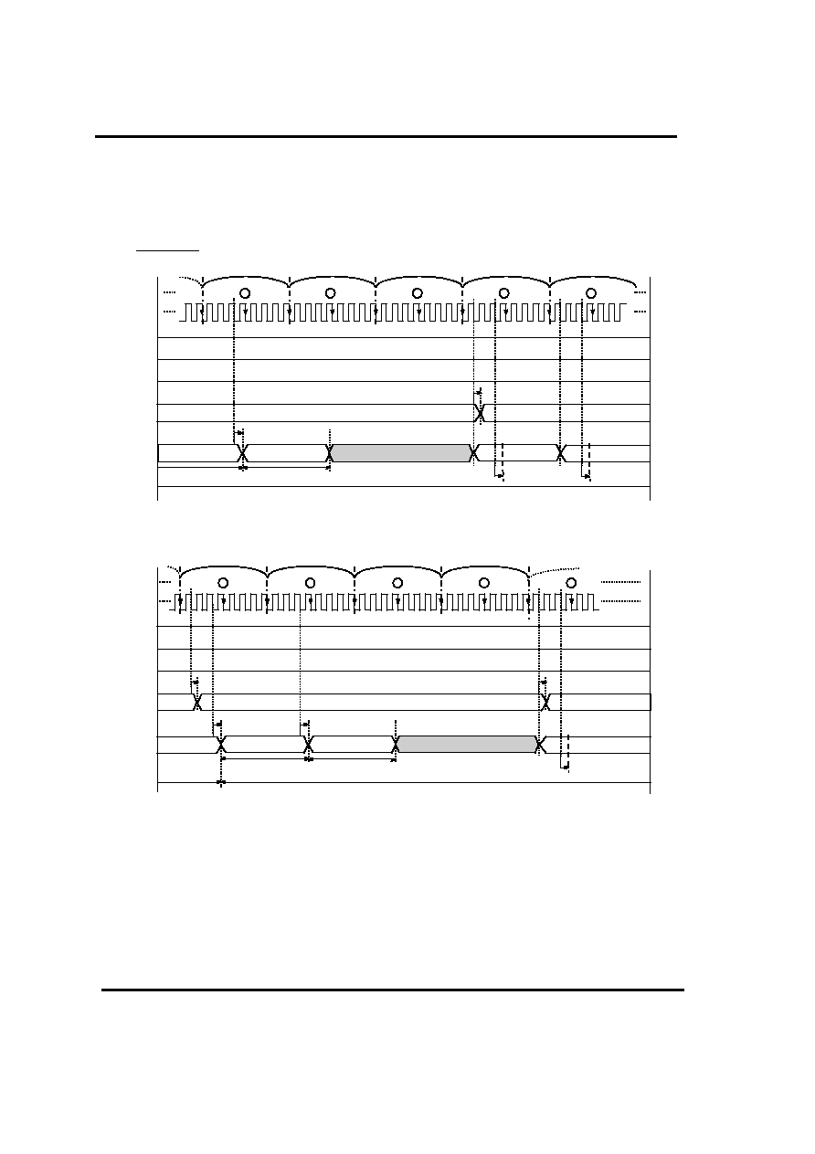
9-11
- Continue -
26&
9''
9
''+
9
,+3
9
''+
.a.
.
.933
'a'
$+
$/
7
'/<
7
+/'
7
'/<
$GGU
%ORFN
%ORFN
%ORFN
%ORFN
%ORFN
7
+/'
2+
7
67%
2/
7
67%
26&
9''
9
''+
9
,+3
9
''+
.a.
.
.933
'a'
%ORFN
%ORFN
%ORFN
%ORFN
7
'/<
7
'/<
7
'/<
2/
$+
$/
7
+/'
7
+/'
7
'/<
$GGU
2+
7
67%
Chapter 9. EPROM

9-12
3) Lock Bit Write Mode
26&
9''
9
''+
7
9335
9
,+3
7
9336
9
''+
7
3
.a.
0+�
.
.933
'a'
[ 7
3
7
.'
7
.6
5HVHW
/RFN :ULWH 0RGH VHWWLQJ
%ORFN
%ORFN
%ORFN
%ORFN
7
02'(
0/�
%ORFN
:DLW F\FOH
0+ +LJK ELW 0RGH ,QSXW /DWFK
0/ /RZ ELW 0RGH ,QSXW /DWFK
#. Note :
1. Internal system is reset at VPP = 12.5V and K2=`Low`
2. OSC1 is made of a block of 8 x Tp clock.
3. From this time when the reset is released (K2=`High`) , OSC1 clock is counted by 1-bolck.
4. If not written during 10 times repeats(120us), repeat the 5 times until all is written.
26&
9''
9
''+
9
,+3
9
''+
.a.
.
.933
'a'
WLPHV UHSHDW
XV [ XV
7
'/<
%ORFN
%ORFN
%ORFN
%ORFN
7
'/<
:DLW F\FOH
Chapter 9. EPROM

9-13
4) Lock Bit Read Mode
26&
9''
9
''+
7
9335
9
,+3
7
9336
9
''+
7
3
.a.
0+�
.
.933
'a'
[ 7
3
7
.'
7
.6
5HVHW
/RFN 5HDG 0RGH VHWWLQJ
%ORFN
%ORFN
%ORFN
%ORFN
7
02'(
0/�
%ORFN
'
/RFN ELW 2XWSXW
7
67%
0+ +LJK ELW 0RGH ,QSXW /DWFK
0/ /RZ ELW 0RGH ,QSXW /DWFK
#. Note :
1. Internal system is reset at VPP = 12.5V and K2=`Low`
2. OSC1 is made of a block of 8 x Tp clock.
3. From this time when the reset is released (K2=`High`) , OSC1 clock is counted by 1-bolck.
4. Lock data is outputted from D5 port.
If you set Lock bit, the output data of D5 is always `H`.
Chapter 9. EPROM

9-14
:ULWH XVLQJ WKH
(3520 :ULWHU
6FUHHQLQJ
Œ KRXUV�
9HULI\ 7HVW XVLQJ
(3520 :ULWHU
)XQFWLRQ 7HVW
XVLQJ 0DQXDO 7HVW
Caution when programming
IDLO
5HVHW
6HW (3520 ZULWH PRGH�
67$57
)LUVW $GGUHVV
Q
Q ‚ Q
(SURP :ULWH
5HSHDW XQWLO QHDU XV
XV
XV #N+]�
9HULI\
DGGUHVV ‚ DGGUHVV
SDVV
IDLO
\HV
QR
QR
\HV
(SURP :ULWH
:ULWH RQH PRUH WLPH�
5HVHW
6HW (SURP 5HDG PRGH�
UHDG DOO DGGUHVV
(1'
IDLO
SDVV
&KDQJH WKH PRGH
933 9 9'' 9�
UHDG DOO DGGUHVV
%ODQN 9HULI\�
SDVV
5HVHW
6HW (SURP 5HDG PRGH�
9'' 9
933 9
&KDQJH WKH PRGH
933 9 9'' 9�
9'' 9
933 9
9'' 9
933 9
5HSRUW
%ODQN 9HULI\
)DLOXUH
ODVW DGGUHVV "
Q "
6HW 933 9
6HW 9'' 9
5HSRUW
3URJUDPPLQJ
)DLOXUH
5HSRUW
3URJUDPPLQJ
2.
5HSRUW
9HULI\
)DLOXUH
ð
Timing Flowchart for Eprom Program / Verify.
Chapter 9. EPROM
Writing should be done at the defined voltage and timing. In case of EPROM mode, programming
voltage is 12.5V. More than defined voltage can give device so great damage to destroy it.
Before writing you had better ascertain the characteristics of socket and socket adapter of EPROM
writer. It can happen to write error when you touch socket adapter or device. We recommend below
flow to improve reliability after writing.

9-15
<HV
1R
IDLO
SDVV
9'' 9
933 9
9'' 9
933 9
5HSRUW
/RFN %LW 5HDG
)DLOXUH
5HVHW
6HW /RFN %LW 5HDG PRGH�
UHDG /RFN %LW'�
&KDQJH WKH PRGH
933 9 9'' 9�
IDLO
SDVV
5HVHW
6HW /RFN %LW 5HDG PRGH�
UHDG /RFN %LW'�
&KDQJH WKH PRGH
933 9 9'' 9�
9'' 9
933 9
(1'
6HW 933 9
6HW 9'' 9
5HSRUW
/RFN %LW 3URJUDPPLQJ
2.
5HVHW
6HW /RFN %LW ZULWH PRGH�
67$57
:DLW F\FOH
Q
Q ‚ Q
/RFN %LW :ULWH
5HSHDW XQWLO QHDU XV
XV
XV #N+]�
Q "
ð
Timing Flowchart for Lock Bit Program / Verify.
Chapter 9. EPROM

MASK ORDER & VERIFICATION SHEET
GMS3 -R
2. Device Information
Package
4. Marking Specification
6. ROM CODE Verification
20 SSOP
16 SOP (150mil)
16 SOP (300mil)
16 DIP
20 SOP
20 DIP
24 SOP
3. Mask Option
Inclusion of
Pull-up
Register
Port
Y/N
R0* R1* R2* R3*
Inclusion of
condensor
for Osc.
Y/N
System
Clock
Selection
focs / 6
fosc / 48
Release of
Stop mode
Port
Y/N
K0 K1 K2 K3 R0* R1* R2* R3*
Status of
D port while
Stop mode
Port
a/b
D0 D1 D2 D3 D4 D5 D6 D7**
5. Delivery Schedule
Mask Sample
Risk Order
Date
. .
Quantity
pcs
pcs
Confirmation
. .
HYNIX Semiconductor Inc. write in below
Customer write in below
Name &
Signature
Verification Date :
Please confirm our verification data.
Check Sum :
TEL :
82-431-270-4078
FAX :
82-431-270-4075
Approval Date : . .
I agree with your verification data and confirm
you to make mask set.
TEL : FAX :
Company Name :
Section Name :
Signature :
@27c256
4. If you use fosc/6, we recommend inclusion of condensor and
fosc/48, no inclusion of condensor
* : Marked port is not available for GMS36/37004
** : Marked port is not available for GMS36/37004/112
5. D6 port is available for GMS37004/112 but
not available for GMS36004/112
1. Don't use WDTR instruction in subroutine.
2. Use Br $ at start (except 0 page ) , end and
unused address in every page.
3. a: State of " L" forcibly, b: Remain the state just before
stop instruction. You must select "a" option when you use
Dport as key application.
Standard Marking
User Marking
R YWW
File Name
Check Sum
Mask Data
E-Mail
( )
. DMP
@27C256
. RHX
User LOGO
HYNIX Semiconductor Inc.
MCU APPLICATION TEAM
1. Customer Information
Company Name
Name & Signature
Tel:
Fax:
Order Date
D8**D9**
24 DIP
HYNIX
R
YWW