 | –≠–ª–µ–∫—Ç—Ä–æ–Ω–Ω—ã–π –∫–æ–º–ø–æ–Ω–µ–Ω—Ç: GMS81024 | –°–∫–∞—á–∞—Ç—å:  PDF PDF  ZIP ZIP |
Document Outline
- ˛ˇ
- ˛ˇ
- ˛ˇ
- ˛ˇ
- ˛ˇ
- ˛ˇ
- ˛ˇ
- ˛ˇ
- ˛ˇ

8-BIT SINGLE CHIP MICROCOMPUTERS
GMS810 SERIES
USER`S MANUAL
∑ GMS81004
∑ GMS81008
∑ GMS81016
∑ GMS81024
∑ GMS81032

Revision 3.0
Published by
MCU Application Team in HYUNDAI ELCETRONICS Co., Ltd.
®œ
HYUNDAI ELECTRONICS Co., Ltd. 1998 All Right Reserved.
Additional information of this manual may be served by HYUNDAI ELECTIONICS Offices in Korea or
Distributors and Representative listed at address directory.
HYUNDAI ELECTIONICS reserves the right to make changes to any Information here in at any time
without notice.
The information, diagrams, and other data in this manual are correct and reliable; however, HYUNDAI
ELECTIONICS Co., Ltd. is in no way responsible for any violations of patents or other rights of the
third party generated by the use of this manual.

Table of Contents
Table of Contents
Chapter 1
Overview
1.1 Features & Pin Assignments . . . . . . . . . . . . . . . . . . . . .
1-1
1.2 Block Diagram . . . . . . . . . . . . . . . . . . . . . . . . . . . . . . .
1-2
1.3 Package Dimension . . . . . . . . . . . . . . . . . . . . . . . . . . .
1-3
1.4 Pin Function . . . . . . . . . . . . . . . . . . . . . . . . . . . . . . . . .
1-5
1.5 Port Structure . . . . . . . . . . . . . . . . . . . . . . . . . . . . . . . .
1-6
1.6 Electrical Characteristics . . . . . . . . . . . . . . . . . . . . . . . .
1-10
Chapter 2
Function Description
2.1 Register . . . . . . . . . . . . . . . . . . . . . . . . . . . . . . . . . . . .
2-1
2.2 Memory Map . . . . . . . . . . . . . . . . . . . . . . . . . . . . . . . . .
2-6
2.3 TCALL Vector Area . . . . . . . . . . . . . . . . . . . . . . . . . . .
2-7
2.4 Zero-Page Peripheral Registers . . . . . . . . . . . . . . . . . . . 2-8
Chapter 3
I/O PORT
3.1 Port R0 . . . . . . . . . . . . . . . . . . . . . . . . . . . . . . . . . . . . . .
3-1
3.2 Port R1 . . . . . . . . . . . . . . . . . . . . . . . . . . . . . . . . . . . . . .
3-2
3.3 Port R2 . . . . . . . . . . . . . . . . . . . . . . . . . . . . . . . . . . . . . .
3-2
Chapter 4
Peripheral Hardware
4.1 Clock Generating Circuit . . . . . . . . . . . . . . . . . . . . . . . . . 4-1
4.2 Timer . . . . . . . . . . . . . . . . . . . . . . . . . . . . . . . . . . . . . . 4-10

Table of Contents
Chapter 5
Interrupt
5.1 Interrupt Source . . . . . . . . . . . . . . . . . . . . . . . . . . . . . . .
5-1
5.2 Interrupt Control Register . . . . . . . . . . . . . . . . . . . . . . . .
5-3
5.3 Interrupt Accept Mode . . . . . . . . . . . . . . . . . . . . . . . . . . .
5-4
5.4 Interrupt Processing Sequence . . . . . . . . . . . . . . . . . . . .
5-7
5.5 Software Interrupt . . .. . . . . . . . . . . . . . . . . . . . . . . . . . .
5-8
5.6 Multiple Interrupt . . . . . . . . . . . . . . . . . . . . . . . . . . . . . .
5-9
5.7 Key Scan Input Processing . . . . . . . . . . . . . . . . . . . . . . .
5-11
Chapter 6
Standby Function
6.1 Stop Mode . . . . . . . . . . . . . . . . . . . . . . . . . . . . . . . . .
6-1
6.2 Standby Mode Release . . . . . . . . . . . . . . . . . . . . . . . . . 6-3
6.3 Release Operation of Standby Mode . . . . . . . . . . . . . . . 6-5
Chapter 7
Reset Function
7.1 External RESET . . . . . . . . . . . . . . . . . . . . . . . . . . . . . . .
7-1
7.2 Power On Reset . . . . . . . . . . . . . . . . . . . . . . . . . . . . . . .
7-1
7.3 Low Voltage Detection Mode . . . . . . . . . . . . . . . . . . . . .
7-4
Appendix
Instruction Set Table
Programmer`s guide
Mask option list

OVERVIEW
1
FUNCTION DESCRIPTION
2
I/O PORT
3
PERIPHERAL HARDWARE
4
INTERRUPT
5
STANDBY FUNCTION
6
RESET FUNCTION
7
APPENDIX A.
8
APPENDIX B.
9

1 - 1
Chapter 1. Overview
CHAPTER 1. OVERVIEW
The GMS810 Series is the high speed and Low voltage operating 8-bit single chip
microcomputers. This MCU contains G8MC core, ROM, RAM, input/output ports and five
multi-function timer/counters.
1.1 FEATURES & PIN ASSIGNMENTS (TOP VIEW)
°·
ROM size . . . . . . . . . . . . . 4,096 Bytes ( GMS81004 ) , 8,192 Bytes (GMS81008 )
. . . . . . . . . . . . . 16,384 Bytes ( GMS81016 ) ,24,576 Bytes(GMS81024 )
. . . . . . . . . . . . . 32,768 Bytes ( GMS81032 )
°·
RAM size . . . . . . . . . . . . . 448 Bytes
°·
Instruction Execution Time . . 1us @Xin=4MHz
°·
Timer
°Ð
Timer/Counter . . . . . .
8Bit * 2ch , 16Bit * 1ch
°Ð
Basic Interval Time . . .
8Bit * 1ch
°Ð
Watch Dog Timer . . . .
6Bit * 1ch
°·
Power On Reset
°·
Power Saving Operation Modes
°Ð
STOP
°·
8 Interrupt Sources
°Ð
Nested Interrupt Control is Available
°·
Operating Voltage
°Ð
2.0~4.0V @2MHz
°Ð
2.2~4.0V @4MHz
°·
Low Voltage Detection Circuit
°·
Watch dog Timer Auto Start ( During 1Second after Power on Reset )
°·
Package
°Ð
20SOP/20PDIP/24SOP/24Skinny DIP/28SOP/28Skinny DIP
°Ð
44PLCC
°·
I/O Port
20pin
24pin
28pin
44pin
input
3
3
3
3
output
2
2
2
2
I/O
13
17
21
24

1 - 2
Chapter 1. Overview
PIN ASSIGNMENT
R11
R10
VDD
XOUT
XIN
R00
R01
R02
R03
R20
1
2
3
4
5
7
8
9
10
6
R16
R17
REMOUT
RESET
TEST
R07
R06
R05
R04
VSS
20
19
18
17
16
15
14
13
12
11
R13
R12
R11
R10
VDD
XOUT
XIN
R00
R01
R02
R03
R20
1
2
3
4
5
7
8
9
10
11
12
6
R14
R15
R16
R17
REMOUT
RESET
TEST
R07
R06
R05
R04
VSS
24
23
22
21
20
19
18
17
16
15
14
13
R14
R15
R16
R17
REMOUT
RESET
TEST
R07
R06
R05
R04
VSS
R24
R23
28
27
26
25
24
23
22
21
20
19
18
17
16
15
R13
R12
R11
R10
VDD
XOUT
XIN
R00
R01
R02
R03
R20
R21
R22
1
2
3
4
5
7
8
9
10
11
12
13
14
6
28PIN
R27
VSS
REMOUT
RESET
TEST
R07
R06
R05
39
38
37
36
35
34
33
32
31
30
29
44PLCC
R25
R26
7
8
9
10
11
12
13
14
VDD
XOUT
XIN
R00
R01
R02
15
16
17
R13
R12
R11
R10
6
5
4
3
2
1
44
43
42
41
40
R14
R15
R16
R17
R22
R21
R20
R03
18
19
20
21
22
23
24
25
26
27
28
R23
R24
VSS
R04
NC
NC
NC
NC
NC
NC
NC
NC
NC
NC
NC
NC
24PIN
24PIN
20PIN

1 - 3
1.2 Block Diagram
`
G8MC
CORE
RAM
(448byte)
ROM
(16K byte)
WATCHDOG
TIMER
TIMER
INTERRUPT
Key scan
INT.
generation
Block
CLOCK
GEN. /
SYSTEM
CONTROL
PRESCALER
/
B.I.T
R0
PORT
R1
PORT
R2
PORT
Vdd
Vss
Xout
Xin
RESET
TEST
R10~R17
R00~R07
R11/INT1
R12/INT2
REMOUT
R17/T0
R16/T1
R15/T2
R14/EC
R00~R07
R10~R17
R20~R27
Chapter 1. Overview

1 - 4
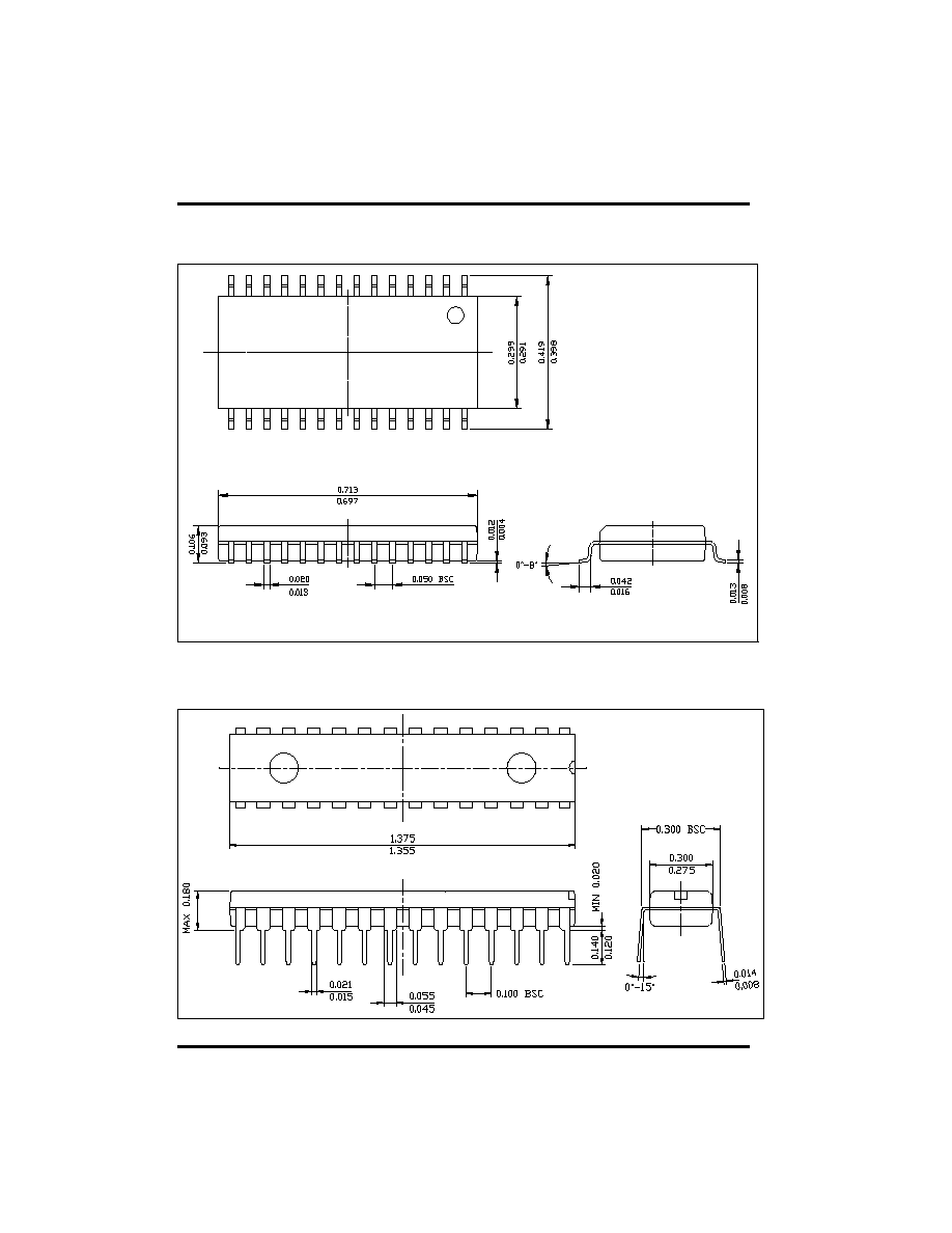
1.3 Package Dimension
Chapter 1. Overview
1.3.1 20SOP Pin Dimension(dimensions in inch)
1.3.2 20PDIP Pin Dimension (dimensions in inch)

1 - 5
Chapter 1. Overview
1.3.3 24SOP Pin Dimension (dimensions in inch)
1.3.4 24skinnyDIP Pin Dimension (dimensions in inch)
1 - 6
Chapter 1. Overview
1.3.5 28SOP Pin Dimension (dimensions in inch)
1.3.6 28skinnyDIP Pin Dimension (dimensions in inch)

1 - 7
1.3.7 44PLCC Pin Dimension (dimensions in mm)
Chapter 1. Overview

1 - 8
1.4 Pin Function
PIN NAME
INPUT/
OUTPUT
Function
@ RESET @ STOP
R00
I/O
INPUT
State
of before
STOP
R01
R02
R03
R04
R05
R06
R07
R10
R11/INT1
R12/INT2
R13
R14/EC
R15/T2
R16/T1
R17/T0
R20
R21
R22
R23
R24
XIN
XOUT
REMOUT
RESET
TEST
VDD
VSS
I/O
I/O
I/O
I/O
I/O
I/O
I/O
I/O
I/O
I/O
I/O
I/O
I/O
I/O
I/O
I/O
I/O
I/O
I/O
I/O
I
O
O
I
I
P
P
- Each bit of the port can be
individually configured as an
input or an output by user
software
- Push-pull output
- CMOS input with pull-up resistor
(option)
- Can be programmable as Key
Scan Input
- Pull-ups are automatically
disabled at output mode
INPUT
State
of before
STOP
- CMOS input with pull-up resistor
(option)
- Push-pull output
- Can be programmable as Key
Scan Input or Open drain output
- Direct Driving of LED(N-TR)
- Pull-ups are disabled at output
mode
INPUT
State
of before
STOP
- CMOS input with pull-up resistor
(option)
- Push-pull output
- Direct Driving of LED(N-TR)
- Pull-ups are disabled at output
mode
Low
High
- Oscillator Input
- Oscillator Output
`L` output
`L` Output
- High Current Output
`L` level
state
of before
STOP
- Includes pull-up resistor
- Includes pull-up resistor
- Positive power supply
- Ground
Chapter 1. Overview
INPUT
20Pin 24Pin 28Pin 44Pin
6
8
8
11
7
9
9
15
8
10
10
16
9
11
11
19
12
14
18
27
13
15
19
30
14
16
20
31
15
17
21
32
2
4
4
5
1
3
3
4
-
2
2
3
-
1
1
2
-
24
28
44
-
23
27
43
20
22
26
42
19
21
25
41
R25
I/O
R26
I/O
R27
I/O
10
12
12
20
-
-
13
21
-
-
14
22
-
-
15
24
-
-
16
25
-
-
-
13
-
-
-
14
-
-
-
36
VSS
P
5
7
7
10
4
6
6
9
18
20
24
38
17
19
23
37
16
18
22
33
3
5
5
8
11
13
17
26
-
-
-
35

1 - 9
1.5 Port Structure
1.5.1 R0 PORT
Chapter 1. Overview
R00
R01
R02
R03
R04
R05
R06
R07
PIN
@ RESET
Hi - Z
OR
High-Input
(with pullup)
MUX
Data Reg
Direction Reg
Data Bus
°Ë
Rd
CIRCUIT TYPE
VDD
VSS
pull-up
option
PAD
VDD
Data Bus
°Ë
Rd

1 - 10
1.5.2 R1 PORT
Chapter 1. Overview
MUX
Data Reg
Direction Reg
Data Bus
R10
R11/INT1
R12/INT2
R13
R14/EC
PIN
CIRCUIT TYPE
@ RESET
Hi - Z
OR
High-Input
(with pullup)
VDD
VSS
pull-up
option
PAD
VDD
T0 R11...INT1
T0 R12...INT2
T0 R14...EC
Rd
open drain
selection
MUX
Data Reg
Direction Reg
Data Bus
R15 / T2
R16 / T1
R17 / T0
Hi - Z
OR
High-Input
(with pullup)
VDD
VSS
pull-up
option
PAD
VDD
Rd
open drain
selection
MUX
from R15...T2
from R16...T1
from R17...T0

1 - 11
1.5.3 R2 PORT
Chapter 1. Overview
REMOUT PORT
internal signal
REMOUT
PIN
CIRCUIT TYPE
@ RESET
Low level
VDD
VSS
PAD
MUX
Data Reg
Direction Reg
Data Bus
R20
R21
R22
R23
R24
R25
R26
R27
PIN
CIRCUIT TYPE
@ RESET
Hi - Z
OR
High-Input
(with pullup)
VDD
VSS
pull-up
option
PAD
VDD
°Ë
Rd

1 - 12
1.5.4 Miscellaneous Ports
Chapter 1. Overview
PIN
CIRCUIT TYPE
@ RESET
RESET
Low level
VSS
PAD
VDD
VSS
from POWER on RESET circuit
pull-up resistor
TEST
High level
PAD
VDD
VSS
pull-up resistor
Xin
Xout
oscillation
Xin
Xout
VSS
from STOP circuit

1 - 13
1.6 Electrical Characteristics
1.6.1 Absolute Maximum Ratings (Ta = 25
°…
)
Chapter 1. Overview
1.6.2 Recommended Operating Ranges
PARAMETER
Supply Voltage
Input Voltage
Output Voltage
Operating Temperature
Storage Temperature
Power Dissipation
SYMBOL
VDD
VI
VO
Topr
Tstg
PD
RATINGS
-0.3 ~ +7.0
-0.3 ~ VDD + 0.3
0 ~ 70
-65 ~ 150
700
-0.3 ~ VDD + 0.3
UNIT
V
V
°…
°…
mW
V
PARAMETER
SYMBOL
CONDITION
UNIT
Supply Voltage
VDD1
VDD2
Operating Temperature
Topr
Oscillation Frequency
fXin
fXin = 1MHz
fXin = 2MHz
fXin = 4MHz
MIN.
TYP.
MAX.
V
V
MHz
°…
2.0
2.2
4.0
4.0
2.0
1.0
0
70
4.0
1.6.2 Recommended Operating Ranges

1 - 14
1.6.3 DC Characteristics (VDD = 2.0~4.0, Vss = 0V, Ta = 0
°…
~ 70
°…
)
Chapter 1. Overview
Parameter
Symbol
Condition
Specification
Unit
max
typ
min
V
DD
0.8V
DD
high level
input voltage
V
IH
1
R11, R12, R14, RESETB
V
IH
2
V
V
V
DD
0.7V
DD
R0, R1(Except R11,R12,R14 ) , R2
V
IL
1
R11, R12, R14, RESETB
V
IL
2
R0, R1(Except R11,R12,R14 ) , R2
low level
input voltage
0.2V
DD
0
0.3V
DD
0
V
V
high level input
leakage current
low level input
leakage current
I
IH
I
IL
V
OH
1
V
OH
2
V
OH
3
V
OL
1
V
OL
2
high level
output voltage
low level
output voltage
high level output
leakage current
low level output
leakage current
I
OHL
I
OLL
I
P
1
RESETB
I
P
2
R0, R1, R2
input pull-up
current
60
30
15
40
20
10
uA
uA
10
4
6
2.4
mA
6
2.4
3
1.2
10
3
---
8
2
---
POWER
SUPPLY
CURRENT
I
DD
operating
current
f
XIN
=4MHz
I
STOP
stop
mode
current
oscillator
stop
R0,R1,R2,RESETB
R0,R1,R2,RESETB
(without pull-up)
R0
R1(ExceptR17),R2
R17
R0
R1, R2
R0, R1, R2
R0, R1, R2
V
IH
=V
DD
V
IL
=0V
I
OH
=-0.5mA
I
OH
=-1mA
I
OH
=-8mA
I
OL
=1mA
I
OL
=5mA
V
OH
=V
DD
V
OL
=0V
V
DD
=3V
V
DD
=3V
f
XIN
=2MHz
V
DD
=4V
V
DD
=2.2V
V
DD
=4V
V
DD
=2V
V
DD
=4V
V
DD
=2V
1
-1
uA
uA
V
DD
-0.4
V
DD
-0.4
V
DD
-0.9
V
V
V
0.4
0.8
V
V
1
-1
uA
uA
mA
mA
mA
uA
uA
I
OL
REMOUT
V
OL
=1V
0.5
-
3
mA
I
OH
REMOUT
V
OH
=2V
-30
-12
-5
mA
RAM retention
supply voltage
V
RET
0.7
V
high level output
current
low level output
current
V
OH
5
OSC
I
OH
=-200uA
V
DD
-0.9
V
V
OL
5
OSC
I
OL
=200uA
0.8
V

1 - 15
°Ð GMS810 Series REMOUT port I
OH
Characteristics graph
°Ð GMS810 Series REMOUT port I
OL
Characteristics graph
Chapter 1. Overview
-35.0
-30.0
-25.0
-20.0
-15.0
-10.0
-5.0
0.0
0
1
2
3
4
VOH(V)
IOH(mA)
VDD=4V
VDD=3V
VDD=2V
0.00
1.00
2.00
3.00
4.00
5.00
6.00
7.00
8.00
0
1
2
3
4
VOL(V)
IOL(mA)
VDD=4V
VDD=3V
VDD=2V

1 - 16
1.6.4 AC Characteristics (VDD = 2.0~4.0, Vss = 0V, Ta = 0
°…
~ 70
°…
)
Chapter 1. Overview
No
Parameter
Symbol
Unit
Pin
Specification
min
typ
max
External clock input cycle time
System clock cycle time
External clock pulse width High
External clock pulse width Low
External clock rising time
External clock falling time
interrupt pulse width High
Interrupt pulse width Low
tcp
ns
Xin
250
500
1000
1
2
3
4
5
6
7
8
Reset input pulse width low
9
tsys
tcpH
tcpL
trcp
tfcp
tIH
tIL
tRSTL
ns
ns
ns
ns
ns
tsys
tsys
tsys
Xin
Xin
Xin
Xin
INT1~INT2
RESET
INT1~INT2
500
1000 2000
40
40
40
40
2
2
8
Event counter input pulse
width high
10
Event counter input pulse
width low
11
Event counter input pulse
rising time
12
Event counter input pulse
falling time
13
tECH
tECL
trEC
tfEC
tsys
tsys
ns
ns
EC
EC
EC
EC
2
2
40
40
* Refer to Fig 1-1

1 - 17
Chapter 1. Overview
RESET
tRSTL
0.2Vcc
EC
tECH
tECL
0.8Vcc
0.8Vcc
0.2Vcc
trEC
tfEC
tIH
INT1
INT2
tIL
0.8Vcc
0.2Vcc
tCP
tCPH
Xin
tCPL
trCP
tfCP
Vcc-0.5V
0.5V
* FIG-1 : Clock, INT, RESET. EC input timing

OVERVIEW
1
FUNCTION DESCRIPTION
2
I/O PORT
3
PERIPHERAL HARDWARE
4
INTERRUPT
5
STANDBY FUNCTION
6
RESET FUNCTION
7
APPENDIX A.
8
APPENDIX B.
9

2 - 1
CHAPTER 2. FUNCTION DESCRIPTION
2.1 REGISTERS
PCH
PCL
A
X
Y
SP
PSW
N
V
G
B
H
I
Z
C
°È
15
7
0
7
0
15
7
0
7
0
7
0
7
0
7
0
°È
Carry Flag
Zero Flag
Interrupt Enable Flag
Half Carry Flag
Break Flag
G Flag
Overflow Flag
Negative Flag
Program Status Word
Stack Pointer
°ÿ
1
Y-Register
X-Register
YA (16bit Accumulator)
A-Register
Program Counter
PCH
PCL
15
7
0
Fixed as 01XXh (=RAM 1page)
°È
°È
SP
°ÿ
1 Stack Address
Chapter 2. Function Description

2 - 2
Chapter 2. Function Description
2.1.1 A register
- 8bit Accumulator.
- In the case of 16-bit operation, compose the lower 8-bit of A, upper 8bit in Y (16-bit
Accumulator)
- In the case of multiplication instruction, execute as a multiplier register. After
multiplication operation, the lower 8-bit of the result enters. (Y*A
°Ê
YA)
- In the case of division instruction, execute as the lower 8-bit of dividend. After
division operation, quotient enters.
2.1.2 X register
- General-purpose 8-bit register
- In the case of index addressing mode within direct page(RAM area), execute as
index register.
- In the case of division instruction, execute as register.
2.1.3 Y register
- General-purpose 8-bit register
- In the case of index addressing mode, execute as index register
- In the case of 16-bit operation instruction, execute as the upper 8-bit of YA (16-bit
accumulator).
- In the case of multiplication instruction, execute as a multiplicand register. After
multiplication operation, the upper 8-bit of the result enters.
- In the case of division instruction, execute as the upper 8-bit of dividend. After
division operation, remains enters.
- Can be used as loop counter of conditional branch command. (e.g.DBNE Y, rel)
2.1.4 Stack Pointer
- In the cases of subroutine call, Interrupt and PUSH, POP, RETI, RET instruction,
stack data on RAM or in the case of returning, assign the storage location having
stacked data.
- Stack area is constrained within 1-page (00H-FFH). The SP is post-decremented
when a subroutine call or a push instruction is executed, or when an interrupt is
accepted; and the SP is pre-incremented when a return or a pop instruction is
executed.
- SP should be initialized as follows
ex) LDX #0FEH
: 0FEH
°Ê
X reg.
TXSP
: X reg.
°Ê
SP
- The behaviors of stack pointer according to each instruction are the following.

2 - 3
Chapter 2. Function Description
2.1.4.1 Interrupt
M(SP)
°Á
(PCH)
SP
°Á
SP - 1
M(SP)
°Á
(PCL)
SP
°Á
SP - 1
M(SP)
°Á
(PSW)
SP
°Á
SP - 1
2.1.4.2 RETI( Return from interrupt )
SP
°Á
SP + 1
(PSW)
°Á
M(SP)
SP
°Á
SP + 1
(PCL)
°Á
M(SP)
SP
°Á
SP + 1
(PCH)
°Á
M(SP)
2.1.4.3 Subroutine call
M(SP)
°Á
(PCH)
SP
°Á
SP - 1
M(SP)
°Á
(PCL)
SP
°Á
SP - 1
2.1.4.4 RET(Return from subroutine)
SP
°Á
SP + 1
(PCL)
°Á
M(SP)
SP
°Á
SP + 1
(PCH)
°Á
M(SP)

2 - 4
2.1.4.5 PUSH A(X, Y, PSW)
M(SP)
°Á
A
SP
°Á
SP - 1
2.1.4.6 POP A(X, Y, PSW)
SP
°Á
SP + 1
A
°Á
M(SP)
2.1.5 PC (Program Counter)
- Program counter is a 16-bit counter consisted of 8-bit register PCH and PCL.
- Addressing space is 64K bytes.
2.1.6 PSW (Program Status Word)
- PSW is an 8-bit register.
- Consisted of the flags showing the post state of operation and the flags determining
the CPU operation, initialized as 00H in reset state.
2.1.7 Flag register.
2.1.7.1 Carry flag (C)
- After operation, set when there is a carry from bit7 of ALU or there is not a borrow.
- Set by SETC and clear by CLRC.
- Executable as 1-bit accumulator.
- Branch condition flag of BCS, BCC.
2.1.7.2 Zero flag (Z)
- After operation also including 16-bit operatiion, set if the result is
°»
0
°»
- Branch condition flag of BEQ, BNE.
2.1.7.3 Interrupt enable flag (I)
- Master enable flag of interrupt except for RST (reset).
- Set and cleared by EI, DI
Chapter 2. Function Description

2 - 5
2.1.7.4 Half carry flag (H)
- After operation, set when there is a carry from bit3 of ALU or there is not a borrow
from bit4 of ALU.
- Can not be set by any instruction.
- Cleared by CLRV instruction like V flag.
2.1.7.5 Break flag (B)
- Set by BRK (S/W interrupt) instruction to distinguish BRK and TCALL instruction
having the same vector address.
2.1.7.6 G flag (G)
- Set and cleared by SETG, CLRG instruction.
- Assign direct page (0-page, 1-page).
- Addressable directly to RAM 1-page by SETG. and to RAM 0-page by CLRG.
2.1.7.7 Overflow flag (V)
- After operation, set when overflow or underflow occurs.
- In the case of BIT instruction, bit6 memory location is transferred to V-flag.
- Cleared by CLRV instruction, but not set by any instruction.
- Branch condition flag of BVS, BVC.
2.1.7.8 Negative flag (N)
- Set whenever the result of a data transfer or operation is negative (bit7 is set to
°»
1
°»
).
- In the case of BIT instruction, bit7 of memory location is transferred to N-flag
- N-flag is not affected by CLR or SET instruction.
- Branch condition flag of BPL, BMI.
Chapter 2. Function Description

2 - 6
2.2 MEMORY MAP
RAM
(192 BYTES)
PERIPHERAL REGISTERS
RAM (STACK)
(256 BYTES)
NON-USE
ROM
(24,576 BYTES)
PCALL AREA
TCALL VECTOR AREA
INTERRUPT VECTOR AREA
0-PAGE
1-PAGE
DIRECT PAGE
PROGRAM ROM
U-PAGE
0000h
00BFh
0100h
0200h
C000h
FF00h
FFC0h
FFE0h
FFFFh
Chapter 2. Function Description
ROM
(8,192 BYTES)
ROM
(4,096 BYTES)
E000h
F000h
ROM
(32,768 BYTES)
8000h
ROM
(16,384 BYTES)
A000h
GMS81004
GMS81008
GMS81016
GMS81032
GMS81024

2 - 7
2.3 TCALL VECTOR AREA
TCALL 15
TCALL 14
TCALL 13
TCALL 12
TCALL 11
TCALL 10
TCALL 9
TCALL 8
TCALL 7
TCALL 6
TCALL 5
TCALL 4
TCALL 3
TCALL 2
TCALL 1
TCALL 0
FFC0h
FFC1h
FFC2h
FFC3h
FFC4h
FFC5h
FFC6h
FFC7h
FFC8h
FFC9h
FFCAh
FFCBh
FFCCh
FFCDh
FFCEh
FFCFh
FFD0h
FFD1h
FFD2h
FFD3h
FFD4h
FFD5h
FFD6h
FFD7h
FFD8h
FFD9h
FFDAh
FFDBh
FFDCh
FFDDh
FFDEh
FFDFh
(L)
(H)
(L)
(H)
(L)
(H)
(L)
(H)
(L)
(H)
(L)
(H)
(L)
(H)
(L)
(H)
(L)
(H)
(L)
(H)
(L)
(H)
(L)
(H)
(L)
(H)
(L)
(H)
(L)
(H)
(L)
(H)
*
*
This vector area is used in BRK command and TCALL0 command.
Chapter 2. Function Description
2 - 8
2.4 ZERO-PAGE PERIPHERAL REGISTERS
ADDRESS
00C0H
FUNCTION REGISTERS
PORT R0 DATA REG.
R/W
R/W
SYMBOL
R0
RESET VALUE
7
6
5
4
3
2
1
0
Undefined
00C1H
PORT R0 DATA DIRECTION REG.
W
R0DD
00
00C2H
PORT R1 DATA REG.
R/W
R1
Undefined
00C3H
PORT R1 DATA DIRECTION REG.
W
R1DD
00
00C4H
PORT R2 DATA REG.
R/W
R2
Undefined
00C5H
PORT R2 DATA DIRECTION REG.
W
R2DD
00
00C6H
Reserved
00C7H
CLOCK CONTROL REG.
W
CKCTLR
BASIC INTERVAL REG.
R
BITR
Undefined
00C8H
WATCH DOG TIMER REG.
W
WDTR
00C9H
PORT R1 MODE REG.
W
PMR1
00
00CAH
INT. MODE REG.
R/W
IMOD
00CBH
EXT. INT. EDGE SELECTION
W
IEDS
00
00CCH
INT. ENABLE REG. HIGH
R/W
IENL
00CDH
INT. REQUEST FLAG REG. LOW
R/W
IRQL
00CEH
INT. ENABLE REG. HIGH
R/W
IENH
00CFH
INT. REQUEST FLAG REG. HIGH
R/W
IRQH
00D0H
TIMER 0 (16bit) MODE REG.
R/W
TM0
00
00D1H
TIMER 1 (8bit) MODE REG.
R/W
TM1
00
00D2H
TIMER 2 (8bit) MODE REG.
R/W
TM2
00
00D3H
TIMER 0 HIGH-MSB DATA REG.
W
T0HMD
Undefined
00D4H
TIMER 0 HIGH-LSB DATA REG.
W
T0HLD
Undefined
00D5H
TIMER0 LOW-MSB DATA REG.
W
T0LMD
Undefined
TIMER0 LOW-MSB COUNT REG.
R
Undefined
-
-
1
1
0
1
1
1
-
0
0
0
1
1
1
1
-
-
0
0
0
0
0
0
-
0
0
-
-
-
-
-
0
0
0
-
0
0
0
-
0
0
0
-
0
0
0
-
-
0
0
-
-
-
-
-
Chapter 2. Function Description
00D6H
TIMER0 LOW-LSB DATA REG.
W
T0LLD
Undefined
TIMER0 LOW-LSB COUNT REG.
R
Undefined
00D7H
TIMER 1 HIGH DATA REG.
W
T1HD
Undefined
00D8H
TIMER1 LOW DATA REG.
W
T1LD
Undefined
TIMER1 LOW COUNT REG.
R
Undefined
00D9H
TIMER2 DATA REG.
W
T2DR
Undefined
TIMER2 COUNT REG.
R
Undefined
00DAH
TIMER 0/ TIMER1 MODE REG.
R/W
TM01
00
00DBH
Reserved
00DCH
STANDBY MODE RELEASE REG0
W
SMRR0
00
00DDH
STANDBY MODE RELEASE REG1
W
SMRR1
00
00DEH
PORT R1 OPEN DRAIN ASSIGN REG.
W
R1ODC
00
- ; Not used
* Caution : Write only register can not be accessed by bit manipulation instruction.
: Do not access the Reserved registers .

OVERVIEW
1
FUNCTION DESCRIPTION
2
I/O PORT
3
PERIPHERAL HARDWARE
4
INTERRUPT
5
STANDBY FUNCTION
6
RESET FUNCTION
7
APPENDIX A.
8
APPENDIX B.
9

3 - 1
Chapter 3. I/O PORT
CHAPTER 3. I/O PORTS
The GMS810series has 21 I/O ports which are PORT0(8 I/O), PORT1 (8 I/O) and
PORT2 (8 I/O). Each port contains data direction register which controls I/O and data
register which stores port data.
3.1 PORT R0
3.1.1 PORT R0 Registers
REGISTER
R0 I/O Data Direction Register
SYMBOL
R/W
RESET VALUE
ADDRESS
R0DD
W
00H
00C1H
R0 Data Register
R0
R/W
Undefined
00C0H
Table 3.1 Port R0 Registers
3.1.2 I/O Data Direction Register (R0DD)
R0DD7
R0DD6
R0DD5
R0DD4
R0DD3
R0DD2
R0DD1
R0DD0
<00C1H>
R0DD
bit
initial value
R/W
7
0
W
6
0
W
5
0
W
4
0
W
3
0
W
2
0
W
1
0
W
0
0
W
R0 I/O Data Direction Register(R0DD) is 8-bit register, and can assign input state or
output state to each bit. If R0DD is
°»
1
°»
, port R0 is in the output state, and if
°»
0
°»
, it is
in the input state. R0DD is write-only register. Since R0DD is initialized as
°»
00H
°»
in
reset state, the whole port R0 becomes input state.
3.1.1 Data Register(R0)
R07
R06
R05
R04
R03
R02
R01
R00
<00C0H>
R0
bit
initial value
R/W
7
X
R/W
6
X
R/W
5
X
R/W
4
X
R/W
3
X
R/W
2
X
R/W
1
X
R/W
0
X
R/W
PORT0 data register (R0) is 8-bit register to store data of port R0.
When setted as the output state by R0DD, and data is written in R0, data is outputted
into R0 pin. When set as the input state, input state of pin is read.
The initial value of R0 is unknown in reset state.

3 - 2
3.2 PORT R1
PIN NAME
R10
R11/INT1
R12/INT2
R13
R14/EC
R15/T2
R16/T1
R17/T0
Fig 3.1 Pin Function of port R1
PORT SELECTION
FUNCTION SELECTION
R10(I/O)
R11(I/O)
R12(I/O)
R13(I/O)
R14(I/O)
R15(I/O)
R16(I/O)
R17(I/O)
INT1 (INPUT)
INT2 (INPUT)
EC (INPUT)
T2 (OUTPUT)
T1 (OUTPUT)
T0 (OUTPUT)
REGISTER
R1 I/O Data Direction Register
SYMBOL
R/W
RESET VALUE
ADDRESS
R1DD
W
00H
00C3H
R1 Data Register
R1
R/W
Undefined
00C2H
Table 3.1 Port R1 Registers
3.2.1 PORT R1 Register
R1 Port Mode Register
PMR1
W
00H
00C9H
R1 Port Open drain Assign
Register
R10DC
W
00H
00CEH
3.2.2 I/O Data Direction Register (R1DD)
R1DD7
R1DD6
R1DD5
R1DD4
R1DD3
R1DD2
R1DD1
R1DD0
<00C3H>
R1DD
bit
initial value
R/W
7
0
W
6
0
W
5
0
W
4
0
W
3
0
W
2
0
W
1
0
W
0
0
W
R1 Data Direction Register(R1DD) is 8-bit register, and can assign input state or output
state to each bit. If R1DD is
°»
1
°»
, port R1 is in the output state, and if
°»
0
°»
, it is in the
input state. R1DD is write-only register. Since R1DD is initialized as
°»
00H
°»
in reset
state, the whole port R1 becomes input state.
Chapter 3. I/O PORT

3 - 3
3.2.3 Data Register(R1)
R17OD
R16OD
R15OD
R14OD
R13OD
R12OD
R11OD
R10OD
<00DEH>
R1ODC
bit
initial value
R/W
7
0
W
6
0
W
5
0
W
4
0
W
3
0
W
2
0
W
1
0
W
0
0
W
R1 Data Register(R1) is 8-bit register to store data of port R1. When set as the output
state by R1DD, and data is written in R1, data is output into R1 pin.
The initial value of R1 is unknown in reset state.
R17
R16
R15
R14
R13
R12
R11
R10
<00C2H>
R1
bit
initial value
R/W
7
X
R/W
6
X
R/W
5
X
R/W
4
X
R/W
3
X
R/W
2
X
R/W
1
X
R/W
0
X
R/W
Port R1 Open Drain Assign Register(R1ODC) is 8bit register, and can assign R1 port as
open drain output port each bit, if corresponding port is selected as output. If R1ODC is
selected as
°»
1
°»
, port R1 is open drain output, and if selected as
°»
0
°»
, it is push-pull
output. R1ODC is write-only register and initialized as
°»
00H
°»
in reset state.
3.2.4 Port R1 Open drain Assign Register (R1ODC)
Chapter 3. I/O PORT

3 - 4
T0S
T1S
T2S
ECS
-
INT2S
INT1S
-
<00C9H>
PMR1
bit
initial value
R/W
7
0
W
6
0
W
5
0
W
4
0
W
3
0
W
2
0
W
1
0
W
0
0
W
3.2.5 Port R1 Mode Register (PMR1)
R1 Port Mode Register(PMR1) is 8-bit register, and can assign the selection mode for
each bit. When set as
°»
0
°»
, corresponding bit of PMR1 acts as port R1 selection mode,
and when set as
°»
1
°»
, it becomes function selection mode.
BIT NAME
T0S
PMR1
Selection Mode
Remarks
Table 3.3 Selection Mode of PMR1
0
1
R17 Sel(I/O)
T0 Sel (Output)
-
Output Port of Timer0
T1S
0
1
R16 Sel (I/O)
T1 Sel (Output)
-
Output Port of Timer1
T2S
0
1
R15 Sel (I/O)
T2 Sel (Output)
-
Output Port of Timer2
ECS
0
1
R14 Sel (I/O)
EC Sel (Input)
-
Input Port of Timer0 Event Input
-
0
1
INT2S
0
1
R12 sel (I/O)
INT2 Sel (Input)
-
Input Port of Timer0 Input capture
INT1S
0
1
R11 Sel (I/O)
INT1 Sel (Input)
-
-
-
PMR1 is write-only register and initialized as
°»
00H
°»
in reset state. Therefore,
becomes Port selection mode. Port R1 can be I/O port by manipulating each R1DD bit,
if corresponding PMR1 bit is selected as
°»
0
°»
.
Chapter 3. I/O PORT

3 - 5
3.3 PORT R2
3.3.1 PORT R2 Registers
REGISTERS
R2 I/O Data Direction Register
SYMBOL
R/W
RESET VALUE
ADDRESS
R2DD
W
00H
00C5H
R2 Data Register
R2
R/W
Undefined
00C4H
Table 3.3 Port R2 Registers
R2DD7
R2DD6
R2DD5
R2DD4
R2DD3
R2DD2
R2DD1
R2DD0
<00C5H>
R2DD
bit
initial value
R/W
7
0
W
6
0
W
5
0
W
4
0
W
3
0
W
2
0
W
1
0
W
0
0
W
3.3.2 I/O Data Direction Register (R2DD)
R2 Data Direction Register(R2DD) is 8-bit register, and can assign input state or output
state or output state to each bit. If R2DD is
°»
1
°»
, port R2 is in the output state, and if
°»
0
°»
, it is in the input state.
R2DD is write-only register. Since R2DD is initialized as
°»
00H
°»
in reset state, the
whole port R2 becomes input state.
R27
R26
R25
R24
R23
R22
R21
R20
<00C4H>
R2
bit
initial value
R/W
7
X
R/W
6
X
R/W
5
X
R/W
4
X
R/W
3
X
R/W
2
X
R/W
1
X
R/W
0
X
R/W
3.3.3 Data Register (R2)
R2 Data Register(R2) is 8-bit register to store data of port R2.
When setted as the output state by R2DD, and data is written in R2, data is output into
R2 pin. When setted as input state, input state of pin is read.
The initial value of R2 is unknown in reset state.
Chapter 3. I/O PORT

OVERVIEW
1
FUNCTION DESCRIPTION
2
I/O PORT
3
PERIPHERAL HARDWARE
4
INTERRUPT
5
STANDBY FUNCTION
6
RESET FUNCTION
7
APPENDIX A.
8
APPENDIX B.
9

4 - 1
Chapter 4. Peripheral Hardware
CHAPTER 4. PERIPHERAL HARDWARE
4.1 CLOCK GENERATING CIRCUIT
Clock generating circuit consists of Clock Pulse Generator(C.P.G), Prescaler, Basic
Interval Timer(B.I.T) and Watch Dog Timer.
The clock applied to the Xin pin divided by two is used as the internal system clock.
Fig. 4.1 Block diagram of clock generating circuit
9
PRESCALER
C.P.G
MUX
WDT (6)
COMPARATOR
Internal Data Bus
0
1
2
3
4
0
5
6
6
WDTON
To Reset
Circuit
IFWDT
WDTCL
IFBIT
5
0
7
0
fcpu
fex
PS1
ENPCK
Peripheral
CKCTLR
BTCL
3
8
OSC
Circuit
B.I.T (8)
6
WDTR
Internal System Clock
5

4 - 2
4.1.1 Oscillation Circuit
Oscillation circuit is designed to be used either with a ceramic resonator or crystal
oscillator. Fig. 4.2-(a) shows circuit diagrams using a crystal (or ceramic) oscillator.
As shown in the diagram, oscillation circuits can be constructed by connecting a
oscillator between Xout and Xin. Clock from oscillation circuit makes CPU clock via
clock pulse generator, and then enters prescaler to make peripheral hardware clock.
alternately, the oscillator may be driven from an external source as shown is Fig. 4.2.-
(b). In the Standby(STOP) mode, oscillatiion stop, Xout state goes to
°»
HIGH
°»
, Xin
state goes to
°»
LOW
°»
, and built-in feed back resistor is disabled.
(a) External Crystal (Ceramic) oscillator circuit
Cout
Cin
Xin
Xout
(b) External clock input circuit
Xin
Xout
External clock
Fig. 4.2 Oscillator configurations
Chapter 4. Peripheral Hardware
Frequency
Resonator Maker
Part Name
Load Capacitor
Operating Voltage
*. Recommendable resonator
4.0MHz
°ÿ
MC type is building in load capacitior.CCR type is chip type.
ZTA4.00MG
Cin=Cout=30pF
2.2 ~ 4.0V
FCR4.0MC5
Cin=Cout=open
2.2 ~ 4.0V
CQ
TDK
FCR4.0M5
Cin=Cout=33pF
2.2 ~ 4.0V
TDK
CCR4.0MC3
Cin=Cout=open
2.2 ~ 4.0V
TDK
KBR- 4.0MKC
Cin=Cout=open
2.2 ~ 4.0V
KYOCERA
KBR- 4.0MSB
Cin=Cout=33pF
2.2 ~ 4.0V
KYOCERA

4 - 3
4.1.2 Prescaler
Prescaler consists of 12-bit binary counter. The clock supplied from oscillation circuit is
input to prescaler (fex). The divided output from each bit of prescaler is provided to
peripheral hardware.
4.1.3 Peripheral hardware clock control
Clock to peripheral hardware can be stopped by bit4 (ENPCK) of CKCTLR Register.
ENPCK is set to
°»
1
°»
in reset state.
PS1
PS2
PS3
PS4
PS5
PS6
PS7
PS8
PS9
PS10
PS11
PS12
B.I.T
Peripheral
PS0
PS1
PS2
PS3
PS4
PS5
PS6
PS7
PS8
PS9
PS10 PS11
PS12
fex
ENPCK
fcpu
fex(MHz)
Freq
Period(s)
4
PS1
PS2
PS3
PS4
PS5
PS6
PS7
PS8
PS9
PS10
PS11
PS12
PS0
2M
1M
500K
250K
125K
62.5K
31.25K
15.63K
7.183K
3.906K
1.953K
0.976K
4M
500n
1u
2u
4u
8u
16u
32u
64u
128u
256u
512u
1024u
250n
Freq
Period(s)
2
1M
500k
250K
125K
62.5K
31.25K
15.63K
7.183K
3.906K
1.953K
0.976K
2M
500n
1u
2u
4u
8u
16u
32u
64u
128u
256u
512u
1024u
0.488K
2048u
Fig. 4.3 Block diagram of Prescaler
Chapter 4. Peripheral Hardware

4 - 4
-
-
WDTON
ENPCK
BTCL
BTS2
BTS1
BTS0
CKCTLR
W <00C7H>
ENPCK
0
1
Peripheral Clock
Stopped
Provided
7
0
Clock Control Register
4.1.4 Basic Interval Timer (B.I.T)
- 8bit binary counter
- Use the bit output of prescaler as input to secure the oscillation stabilization time
after power-on
- Secures the oscillation stabilization time in standby mode (stop mode) release
- Contents of B.I.T can be read
- Provides the clock for watch dog timer.
-
-
WTON
ENPCK
BTCL
BTS2
BTS1
BTS0
MUX
BIT0
BIT1
BIT2
BIT3
BIT4
BIT5
BIT6
BIT7
CKCTLR
BITR
IFBIT
PS3
PS4
PS5
PS6
PS7
PS8
PS9
PS10
DATA BUS
Fig. 4.4 Block diagram of Basic Interval Timer
Chapter 4. Peripheral Hardware
DATA BUS

4 - 5
4.1.4.1 Control of B.I.T
If bit3(BTCL) of CKCTLR is set to
°»
1
°»
, B.I.T is cleared, and then, after one machine
cycle, BTCL becomes
°»
0
°»
, and B.I.T starts counting. BTCL is set to
°»
0
°»
in reset
state.
-
-
WDTON
ENPCK
BTCL
BTS2
BTS1
BTS0
CKCTLR
W <00C7H>
BTCL
0
1
B.I.T Operation
free-run
Automatically cleared, after one cycle
7
0
Clock Control Register
4.1.4.2 Input Clock Selection of Basic Interval Timer
The input clock of B.I.T can be selected from the prescaler within a range of 2us to
256us by clock input selection bits(BTS2~BTS0). (at fex = 4MHz).
In reset state, or power on reset, BTS2=1, BTS1=1, BTS0=1 to secure the longest
oscillation stabilization time.
B.I.T can generate the wide range of basic interval time interrupt request(IFBIT) by
selecting prescaler output.
Interrupt interval can be selected to 8 kinds of interval time as shown in Table. 4.1.
Chapter 4. Peripheral Hardware

4 - 6
-
-
WDTON
ENPCK
BTCL
BTS2
BTS1
BTS0
CKCTLR
W <00C7H>
BTS2
0
0
7
0
4.1.4.3 Reading Basic Interval Timer
By reading of the Basic Interval Timer Register(BITR), we can read counter value of
B.I.T. Because B.I.T can be cleared or read, the spending time up to maximum 65.5ms
can be available. B.I.T is read-only register. If B.I.T register is written, then CKCTLR
register with same address is written.
BTS1
0
0
BTS0
0
1
B.I.T. Input clock
PS3 (2us)
PS4 (4us)
Standby release time
512 us
1,024 us
0
0
1
1
0
1
PS5 (8us)
PS6 (16us)
2,048 us
4,096 us
1
1
0
0
0
1
PS7 (32us)
PS8 (64us)
8,192 us
16,384 us
1
1
1
1
0
1
PS9 (128us)
PS10 (256us)
32,768 us
65,536 us
Table 4.1 Standby release time according to BTS
BIT7
BIT6
BIT5
BIT4
BIT3
BIT2
BIT1
BIT0
BITR
R <00C7H>
7
0
Basic Interval Timer Register
Chapter 4. Peripheral Hardware

4 - 7
4.1.5 Watch Dog Timer
Watch Dog Timer(WDT) consists of 6-bit binary counter, 6-bit comparator, and Watch
Dog Timer Register (WDTR).
WDT0
WDT1
WDT2
WDT3
WDT4
WDT5
IFBIT
0
5
6BIT COMPARATOR
WDTR
0
6
WDTR0
WDTR1
WDTR2
WDTR3
WDTR4
WDTR5
WDTCL
W <00C8H>
IF WDT
CLR
WDTON
To Reset circuit
Fig. 4.5 Block diagram of Watch Dog Timer
4.1.5.1 Control of WDT
Watch Dog Timer can be used 6-bit general Timer or specific Watch dog timer by setting
bit5(WDTON) of Clock Control Register(CKCTLR).
-
-
WDTON
ENPCK
BTCL
BTS2
BTS1
BTS0
CKCTLR
W <00C7H>
WDTON
0
1
Watch Dog Timer Function Control
6-bit Timer
Watch Dog Timer
7
0
Clock Control Register
Internal Data Bus
Chapter 4. Peripheral Hardware

4 - 8
By assigning bit6(WDTCL) of WDTR, 6-bit counter can be cleared
-
WDTCL
WDTR5
WDTR4
WDTR3
WDTR2
WDTR1
WDTR0
WDTR
W <00C8H>
WDTCL
0
1
Watch Dog Timer Operation
Free-run
Automatically cleared, after one machine cycle
7
0
Watch Dog Timer Register
Determine Interval of IFWDT
Interval of IFWDT = Value of WDTR
°ø
Interval of IFBIT
(Caution) : after WDTCL = 1, timer maximum error is one cycle of IFBIT.
4.1.5.2 WDT Interrupt Interval
WDT Interrupt(IFWDT) interval is determined by the interrupt IFBIT interval of Basic
Interval Timer and the value of WDT Register.
Interval of IFWDT = (IFBIT interval) * (WDTR value)
Interval of IFWDT : 512us
°ø
1 = 512us (MIN>)
: 65,536us
°ø
63 = 4,128,768us (MAX>)
As IFBIT (Basic Interval Timer Interrupt Request) is used for input clock of WDT, Input
clock cycle is possible from 512us to 65,536us by BTS. (at fex = 4MHz)
*At Hardware reset time ,WDT starts automatically.Therefore, the user must select
the CKCTLR,WDTR before WDT overflow.
( Reset WDTR value = 0Fh,15
interval of WDT = 65,536
°ø
15 = 983040 uS (about 1second ) )
Chapter 4. Peripheral Hardware

4 - 9
-
-
WDTON
ENPCK
BTCL
BTS2
BTS1
BTS0
CKCTLR
W <00C7H>
BTS2
0
0
7
0
BTS1
0
0
BTS0
0
1
Input clock of WDT
Max. Interval of WDT
output (*note1)
32,756 us
64,512 us
0
0
1
1
0
1
129,024 us
258,048 us
1
1
0
0
0
1
516,096 us
1,032,192 us
1
1
1
1
0
1
2,064,384 us
4,128,768 us
*note1) When WDTR Register value is 63(3FH)
Caution : Do not use
°»
0
°»
for WDTR Register value.
Device come into the reset state by WDT
512 us
1,024 us
2,048 us
4,096 us
8,192 us
16,384 us
32,768 us
65,536 us
Chapter 4. Peripheral Hardware

4 - 10
4.2 TIMER
4.2.1 Timer operation mode
Timer consists of 16bit binary counter Timer0(T0), 8bit binary Timer1(T1), Timer2(T2),
Timer Data Register, Timer Mode Register (TM01, TM0, TM1, TM2) and control circuit.
Timer Data Register Consists of Timer0 High-MSB Data Register(T0HMD), Timer0 High-
LSB Data Register(T0HLD), Timer0 Low-MSB Data Register(T0LMD), Timer0 Low-LSB
Data Register(T0LLD), Timer1 High Data Register(T1HD), Timer1 Low Data
Register(T1LD), Timer2 Data Register(T2DR).
Any of the PS0~PS5, PS11 and external event input EC can be selected as clock source
for T0. Any of the PS0~PS3, PS7~PS10 can be selected as clock T1. Any of the
PS5~PS12 can be selected as clock source for T2.
Timer0
- 16-bit Interval Timer
- 16-bit Event Counter
- 16-bit Input Capture
- 16-bit rectangular-wave output
Timer1
- 8-bit Interval Timer
-8-bit rectangular-wave output
Timer2
- 8-bit Interval Timer
-8-bit rectangular-wave output
- Modulo-N Mode
- Single/Modulo-N Mode
- Timer Output Initial Value Setting
- Timer0~Timer1 combination Logic Output
- One Interrupt Generating Every 2nd Counter Overflow
Chapter 4. Peripheral Hardware
*Relevant Port Mode Register (PMR1 : 00C9H) value should be assigned for event counter,
rectangular-wave output and input capture mode.

4 - 11
TIMER0 (16 BIT)
Polarity
Selection
T0HMD
T0HLD
T0LMD
T0LLD
Tout LOGIC
T1 HD
T1 LD
TIMER1 (8 BIT)
T2DR
TIMER2 (8 BIT)
EDGE
Selection
T2 OUT/R15
T1 OUT/R16
REMOUT
T0 OUT/R17
EC/R14
INT2/R12
(Capture
Signal)
16
8
8
8
8
8
8
Fig. 4.6 Timer/Counter Block diagram
Chapter 4. Peripheral Hardware
16

4 - 12
4.2.2 Function of Timer & Counter
16bit Timer (T0)
8bit Timer (T1)
8bit Timer (T2)
Resolution (CK)
MAX.Count
Resolution (CK)
MAX.Count
Resolution (CK)
MAX.Count
PS0
( 0.25us)
16,384us
PS0
(0,.25us)
64us
PS5
( 8us)
2.048us
PS1
( 0. 5us)
32,768us
PS1
( 0,5us)
128us
PS6
( 16us)
4,096us
PS2
( 1us)
65,536us
PS2
( 1us)
256us
PS7
( 32us)
8,192us
PS3
( 2us)
131,072us
PS3
( 2us)
512us
PS8
( 64us)
16,384us
PS4
( 4us)
262,144us
PS7
( 32us)
8,192us
PS9
( 128us)
32,768us
PS5
( 8us)
524,288us
PS8
( 64us)
16,384us
PS10 ( 256us)
65,536us
PS11 (512us)
33,554,432us
PS9
( 128us)
32,768us
PS11 ( 512us)
131,072us
EC
-
PS10 (256us)
65,536us
PS12 (1,024us)
262,144us
fex = 4MHz
Chapter 4. Peripheral Hardware

4 - 13
Internal Data Bus
7
6
5
4
3
2
1
0
TIMER0 H
COUNT
REG
TIMER0 L
COUNT
REG
TIMER0
HM
DATA
REG
TIMER0
HL
DATA
REG
TIMER0
LM
DATA
REG
TIMER0
LL
DATA
REG
SINGLE/
MODULO-N
SELECTION
MUX
CK
T0 COUNTER
(16 BIT)
Clear
PS0
PS1
PS2
PS3
PS4
PS5
PS11
EC
M
U
X
D
E
L
A
Y
EDGE
SELECTION
MUX
Int.
Gen.
OUTPUT GEN.
TM0
R/W
<00D0H>
<00D5H>
<00D6H>
<00D3H> <00D4H>
<00D5H>
<00D6H>
16
16
16
INT2
T0INT
T0 OUT
IFT0
Fig. 4.7 Block Diagram of Timer0
Chapter 4. Peripheral Hardware
DATA READ

4 - 14
TM0
R/W <00D0H>
7
0
T0SL2
T0SL1
T0SL0
Input Clock Sel.
Notes
0
0
0
0
1
1
1
1
0
0
1
1
0
0
1
1
0
1
0
1
0
1
0
1
PS0
(250ns)
PS1
(500ns)
PS2
( 1us)
PS3
( 2us)
PS4
( 4us)
PS5
( 8us)
PS11 (512us)
EC
*
Event
Counter
T0IFS
Timer0 Interrupt Sel.
0
1
Interrupt Every Counter Overflow
Interrupt Every 2nd Counter Overflow
CAP0
T0ST
T0CN
T0MOD
T0IFS
T0SL2
T0SL1
T0SL0
T0MOD
Timer0 Single / Modulo-N Sel.
0
1
Modulo-N
Single Mode
T0CN
Timer0 Counter Continuation / Pause Control
0
1
Count Pause
Count Continuation
T0ST
Timer0 Start/Stop control
0
1
Timer0 Stop
Timer0 Start after Clear
CAP0
Timer0 Interrupt Sel.
0
1
Timer/Counter
Input Capture*
*PS1 : not supporting input capture.
Chapter 4. Peripheral Hardware
Timer0 mode Register

4 - 15
Internal Data Bus
7
6
5
4
3
2
1
0
TIMER1
COUNT REG
TIMER1
H
DATA
REG
TIMER1
L
DATA
REG
SINGLE/
MODULO-N
SELECTION
MUX
CK
T1 COUNTER
(8 BIT)
PS0
PS1
PS2
PS3
PS7
PS8
PS9
PS10
Int.
Gen.
OUTPUT GEN.
TM1
R/W
<00D1H>
<00D7H>
<00D8H>
T1OUT
IFT1
Fig. 4.8 Block Diagram of Timer1
OUTPUT GEN.
X
<00D8H>
T1INT
Chapter 4. Peripheral Hardware

4 - 16
TM1
R/W <00D1H>
7
0
T1SL2
T1SL1
T1SL0
Input Clock Sel.
0
0
0
0
1
1
1
1
0
0
1
1
0
0
1
1
0
1
0
1
0
1
0
1
PS0
(250ns)
PS1
(500ns)
PS2
( 1us)
PS3
( 2us)
PS7
( 32us)
PS8
( 64us)
PS9
(128us)
PS10 (256us)
T1IFS
Timer1 Interrupt Sel.
0
1
Interrupt Every Counter Overflow
Interrupt Every 2nd Counter Overflow
T1ST
T1CN
T1MOD
T1IFS
-
T1SL2
T1SL1
T1SL0
T1MOD
Timer1 Single / Modulo-N Sel.
0
1
Modulo-N
Single Mode
T1CN
Timer1 Countern Continuation / Pause Control
0
1
Count Pause
Count Continuation
Timer1 mode Register
T1ST
Timer1 Start/Stop control
0
1
Timer1 Stop
Timer1 Start after Clear
Chapter 4. Peripheral Hardware

4 - 17
TM01
R/W <00DAH>
7
0
T0UT1
T0UT0
TOUT LOGIC
0
0
1
1
0
1
0
1
AND of T0 OUTPUT and T1 OUTPUT
NAND of T0 OUTPUT and T1 OUTPUT
OR of T0 OUTPUT and T1 OUTPUT
NOR of T0 OUTPUT and T1 OUTPUT
T1INIT
Timer1 Output Initial Value
0
1
Timer1 Output Low
Timer1 Output HIgh
TOUTS
TOUTB
-
T0OUTP
T0INIT
T1INIT
TOUT1
TPIT0
T0INIT
Timer0 Output Initial Value
0
1
Timer0 Output Low
Timer0 Output High
T0OUTP
T0OUTPolarity Selection
0
1
T0OUT Polarity Equal to TOUT Logic Input Signal
T0OUT Polarity Reverse to TOUT Logic Input Signal
TOUTB
REMOUT Port Bit Control
0
1
REMOUT Output Low
REMOUT Output High
TOUTS
REMOUT Port Output Selection
(TOUT Logic or TOUTB)
0
1
Bit(TOUTB) Output Through REMOUT
TOUT Logic Output Through REMOUT
Timer0/Timer1 mode Register
Chapter 4. Peripheral Hardware

4 - 18
Internal Data Bus
7
6
5
4
3
2
1
0
TIMER2
COUNT REG
MUX
CK
T2 COUNTER
(8 BIT)
PS5
PS6
PS7
PS8
PS9
PS10
PS11
PS12
OUTPUT GEN.
TM2
R/W
<00D2H>
<00D9H>
T2 OUT
Fig. 4.9 Block Diagram of Timer2
<00D9H>
TIMER2
DATA REG
IFT2
Chapter 4. Peripheral Hardware

4 - 19
TM2
R/W <00D2H>
7
0
T2SL2
T2SL1
T2SL0
Input Clock Sel.
0
0
0
0
1
1
1
1
0
0
1
1
0
0
1
1
0
1
0
1
0
1
0
1
PS5
( 8us)
PS6
( 16us)
PS7
( 32us)
PS8
( 64us)
PS9
( 128us)
PS10 ( 256us)
PS11 ( 512us)
PS12 (1,024us)
T2cn
Timer2 Counter Continuation / Pause Control
0
1
Count Pause
Count Continuation
-
-
-
T2ST
T2CN
T2SL2
T2SL1
T2SL0
T2ST
Timer2 Start / Stop Control
0
1
Timer2 Stop
Timer2 Start after Clear
Chapter 4. Peripheral Hardware
Timer2 mode Register

4 - 20
PMR1
W <00C9H>
7
0
T0S
T1S
T2S
ECS
-
INT2S
INT1S
-
PORT mode Register1
PMR1
T0S
PORT Sel.
Remarks
0
1
-
Output Port of Timer0
R17 (I/O)
T0 (Output)
T1S
0
1
-
Output Port of Timer1
R16 (I/O)
T1 (Output)
T2S
0
1
-
Output Port of Timer2
R15 (I/O)
T2 (Output)
ECS
0
1
-
Input Port of Timer0 Event
R14 (I/O)
EC (Input)
-
-
-
-
-
-
-
INT2S
0
1
-
Input Port of Timer0 Input Capture
R12 (I/O)
INT2 (Input)
INT1S
0
1
-
-
R11 (I/O)
INT1 (Input)
-
-
-
-
-
-
-
IEDS
W <00CBH>
7
0
-
-
IED2H
IED2L
IED1H
IED1L
-
-
External Interrupt Signal Edge Selectin Register
IED*H
IED*L
INT*
0
0
1
1
--
FallingEdge Selection
Rising Edge Selection
Both Edge Selection
0
1
0
1
Chapter 4. Peripheral Hardware

4 - 21
4.2.3 Timer0, Timer1
TIMER0 and TIMER1 have an up-counter. When value of the up-counter
reaches the content of Timer Data Register(TDR), the up-counter is cleared to
°»
00H
°»
, and interrupt(IFT0, IFT1) is occured at the next clock
Fig. 4. 10 Operatiion of Timer0
Concurrence
Concurrence
Concurrence
CLEAR
CLEAR
CLEAR
0
T0 Data
Registers
Value
T0 Value
INTERRUPT
INTERRUPT
INTERRUPT
Interval period
IFT0
For Timer0, the internal clock(PS) and the external clock(EC) can be selected as
counter clock. But Timer1 and Timer2 use only internal clock. As internal clock.
Timer0 can be used as internal-timer which period is determined by Timer Data
Register(TDR). Chosen as external clock, Timer0 executes as event-counter.
The counter execution of Timer0 and Timer1 is controlled by T0CN, T0ST,
CAP0, T1CN, T1ST, of Timer Mode Register TM0 and TM1. T0CN, T1CN are
used to stop and start Timer0 and Timer1 without clearing the counter. T0ST,
T1ST is used to clear the counter. For clearing and starting the counter, T0ST
or T1ST should be temporarily set to
°»
0
°»
and then set to
°»
1
°»
. T0CN,
T1CN, T0ST and T1ST should be set
°»
1
°»
, when Timer counting-up.
Controlling of CAP0 enables Timer0 as input capture. By programming of CAP0
to
°»
1
°»
, the period of signal from INT2 can be measured and then, event
counter value for INT2 can be read.
Chapter 4. Peripheral Hardware

4 - 22
Concurrence
CLEAR
INTERRUPT
Concurrence
CLEAR
INTERRUPT
IFT0
T0ST
T0CN
0
0
1
0
1
Counter
Count
Stop
Clear
& Count
Stop
Count
continue
Clear & Start
Fig. 4. 11. Start/Stop operation of Timer0
Fig. 4. 12. Input capture operation of Timer0
T0
T1
T2
T3
INT0
Chapter 4. Peripheral Hardware
T0 Data
Register
Value
T0 Value
Clear & Start

4 - 23
During counting-up, value of counter can be read. Timer execution is stopped by the
reset signal (RESET =
°»
L
°»
)
(Note) in the process of reading 16-bit Timer Data, first read the upper 8-bit data. Then
read the lower 8-bit data, and read the upper 8-bit data again. If the earlier read upper
8-bit data are matched with the later read upper 8-bit data, read 16-bit data are correct.
If not, caution should be taken in the selection of upper 8-bit data.
Example)
1) Upper
8-bit
Read
0A
0A
2) Lower
8-bit
Read
FF
01
3) Upper
8-bit
Read
0B
0B
°È °È
4.2.3.1 Single/Modulo-N Mode
Timer0 (Timer1) can select initial (T0INIT, T1INIT of TM0, TM1) output level of Timer
Output port. If initial level is
°»
L
°»
, Low-Data Register value of Timer Data Register is
transferred to comparator and T0OUT(T1OUT) is to be
°»
Low
°»
, if initial level is
°»
High
°»
, High -Data Register is transferred and to be
°»
High
°»
. Single Mode can be
set by Mode Select bit(T0MOD, T1MOD) of Timer Mode Register (TM0, TM1) to
°»
1
°»
When used as Single Mode, Timer counts up and compares with value of Data Register.
If the result is same, Time Out interrupt occurs and level of Timer Output port toggle,
then counter stops as reset state. When used as Modulo-N Mode, T0MOD(T1MOD)
should be set
°»
0
°»
. Counter counts up until the value of Data Register and occurs
Time-out interrupt. The level of Timer Output port toggle and repeats process of
counting the value which is selected in Data Register. During Modulo-N Mode, If
interrupt select bit(T0IFS, T1IFS) of Mode Register is
°»
0
°»
, Interrupt occurs on every
Time-out. If it is
°»
1
°»
, Interrupt occurs every second time-out.
(*note. Timer Output is toggled whenever time out happen)
0AFF 0B01
Chapter 4. Peripheral Hardware

4 - 24
8bit / 16bit
counting
8bit / 16bit
counting
Timer Enable initial.
value toggle.
Timer-output toggle.
interrupt occurs.
count stop.
Timer Enable initial.
value toggle.
Timer-Output Toggle.
Int occurs(IFS = 1) Each 2nd time out.
Int occurs(IFS = 0) When Time out.
< Single Mode >
< Modulo-N Mode >
Fig. 4. 13 Operation Diagram for Single/Modulo-N Mode
Chapter 4. Peripheral Hardware

4 - 25
4.2.4 Timer2
Timer2 operates as a up-counter. The content of T2DR are compared with the
contents of up-counter. If a match is found. Timer2 interrupt (IFT2) is generated
and the up-counter is cleared to
°»
00H
°»
. Therefore, Timer2 executes as a
interval timer. Interrupt period is determined by the count source clock for the
Timer2 and content of T2DR.
When T2ST is set to 1, count value of Timer 2 is cleared and starts counting-
cup. For clearing and starting the Timer2. T2ST have to set to
°»
1
°»
after set to
°»
0
°»
. In order to write a value directly into the T2DR, T2ST should be set to
°»
0
°»
. Count value of Timer2 can be read at any time.
Fig. 4. 14 Operation of Timer2
Concurrence
Concurrence
Concurrence
CLEAR
CLEAR
CLEAR
0
T2 Data
Registers
Value
T2 Value
INTERRUPT
INTERRUPT
INTERRUPT
Interval period
IFT0
Chapter 4. Peripheral Hardware

4 - 26
Concurrence
CLEAR
INTERRUPT
Concurrence
CLEAR
INTERRUPT
IFT2
T2ST
0
count stop by 0
count start clear by 1
Counter
Count up
Count
continue
Count up after clear
Fig. 4. 15. Start/Stop of Timer2
T2 Data
Register
Value
T2 Value
Count Stop
Chapter 4. Peripheral Hardware

OVERVIEW
1
FUNCTION DESCRIPTION
2
I/O PORT
3
PERIPHERAL HARDWARE
4
INTERRUPT
5
STANDBY FUNCTION
6
RESET FUNCTION
7
APPENDIX A.
8
APPENDIX B.
9

5 - 1
CHAPTER 5. INTERRUPT
The GMS810 Series contains 8 interrupt sources; 3 externals and 5 internals. Nested
interrupt services with priority control is also possible. Software interrupt is non-
maskable interrupt, the others are all maskable interrupts.
- 8 interrupt source (2Ext, 3Timer, BIT, WDT and Key Scan)
- 8 interrupt vector
- Nested interrupt control is possible
- Programmable interrupt mode
°Ð
Hardware accept mode
°Ð
Software selection accept mode
- Read and write of interrupt request flag are possible.
- In interrupt accept, request flag is automatically cleared.
Interrupt hardware consists of Interrupt Mode Register(MOD), Interrupt Enable Register
High (IENH), Interrupt Enable Register Low(IENL), Interrupt Request Register
High(IRQH), Interrupt Request Register Low(IRQL) and priority circuit. Interrupt function
block diagram is shown in Fig. 5.1
5.1 INTERRUPT SOURCE
Each interrupt vector is independent and has its own priority. Software interrupt(BRK) is
also available. Interrupt source classification is shown in Table 5.1
Chapter 5. Interrupt

5 - 2
Internal Data Bus
-
-
-
-
-
-
-
-
-
-
KSCNR
INT1R
INT2R
T0R
T1R
T2R
WDTR
BITR
PRIORITY
CONTROL
0
7
0
7
0
7
IENL
IENH
IMOD
IRQ
KSCN
INT1
INT2
IFT0
IFT1
IFT2
IFWDT
IFBIT
INT.
VECTOR
ADDR.
BRK
Standby Mode Release
Fig. 5.1 Interrupt Source
Hardware
Interrupt
Mask
Non-maskable
Priority
-
Interrupt Source
RST (RESET PIN)
INT Vector H
FFFF
INT Vector L
FFFE
Maskable
0
KSCNR (Key Scan)
FFFB
FFFA
1
INT1R(External Interrupt 1)
FFF9
FFF8
2
INT2R(External Interrupt 2)
FFF7
FFF6
3
T0R (Timer0)
FFF3
FFF2
4
T1R (Timer1)
FFF1
FFF0
5
T2R (Timer2)
FFEF
FFEE
6
WDTR (Watch Dog Timer)
FFE9
FFE8
7
BITR (Basic Interval Timer)
FFE7
FFE6
Table 5.1 Interrupt Source
Chapter 5. Interrupt
-
-
BRK Instruction
FFDF
FFDE
Software
Interrupt

5 - 3
5.2 INTERRUPT CONTROL REGISTER
I flag of PSW is a interrupt mask enable flag. When I flag =
°»
0
°»
, all interrupts become
disable. When I flag =
°»
1
°»
, interrupts can be selectively enabled and disabled by
contents of corresponding Interrupt Enable Register.
When interrupt is occured, interrupt request flag is set, and Interrupt request is detected
at the edge of interrupt signal. The accepted interrupt request flag is automatically
cleared during interrupt cycle process. The interrupt request flag maintains
°»
1
°»
until
the interrupt is accepted or is cleared in program.
In reset state, interrupt request flag register(IRQH, IRQL) is cleared to
°»
0
°»
. It is
possible to read the state of interrupt register and to mainpulate the contents of register
and to generate interrupt. (Refer to software interrupt).
-
WDTR
BITE
-
-
-
-
-
IENL
R/W <00CCH>
7
0
Interrupt Enable Register Low
KSCNE
INT1E
INT2E
-
T0E
T1E
T2E
-
IENH
R/W <00CEH>
7
0
Interrupt Enable Register High
-
WDTR
BITE
-
-
-
-
-
IRQL
R/W <00CDH>
7
0
Interrupt Request Register Low
KSCNR
INT1R
INT2R
-
T0R
T1R
T2R
-
IRQH
R/W <00CFH>
7
0
Interrupt Request Register High
Chapter 5. Interrupt

5 - 4
5.3 INTERRUPT ACCEPT MODE
The interrupt priority order is determined by bit(IM1, IM0) of IMOD register.
-
-
IM1
IM0
IP3
IP2
IP1
IP0
IMOD
R/W <00CAH>
7
0
Interrupt Mode Register
IM1
IM0
Priority
0
0
Fixed by H/W
0
1
Changeable by IP 3-0
1
*
Interrupt is inhibited
5.3.1 Selection of interrupt by IP3 - IP0
The condition allow for accepting interrupt is set state of the interrupt mask enable flag
and the interrupt enable bit must be
°»
1
°»
.
IP3
0
0
0
0
0
0
0
1
1
1
1
1
IP2
0
0
0
1
1
1
1
0
0
0
0
1
IP1
0
1
1
0
0
1
1
0
0
1
1
0
IP0
1
0
1
0
1
0
1
0
1
0
1
0
Selection interrupt
KSCNR (Key Scan)
INT1R (External interrupt 1)
INT2R (External interrupt 2)
Reserved
T0R (Timer 0)
T1R (Timer 1)
T2R (Timer 2)
Reserved
Reserved
WDTR (Watch Dog Timer)
BITR (Basic Interval Timer)
Reserved
Table 5.2 Interrupt Selection by IP3 - IP0
Chapter 5. Interrupt
Assigning by interrupt accept mode bit
*In Reset state, these IP3 - IP0 registers become all
°»
0
°»
.

5 - 5
5.3.2 Interrupt Timing
CLOCK
SYNC
A command before interrupt
interrupt process step
Interrupt Request Sampling
Fig. 5.2 Interrupt Enable Accept Timing
Interrupt Request
sampling time
Maximum 12 machine cycle (When execute DIV instruction)
Minimum 0 machine cycle
Interrupt overhead
Maximum 1 + 12 + 8 = 21 machine cycle
Minimum 1 + 0 + 8 = 9 machine cycle
5.3.3 The valid timing after executing Interrupt control instructions
I flag is valid just after executing of EI/DI on the contrary.
Interrupt Enable register is valid one instruction after controlling interrupt Enable
Register.
Interrupt preprocess step is 8 machine cycle
Chapter 5. Interrupt

5 - 6
5.4 INTERRUPT PROCESSING SEQUENCE
When an interrupt is accepted, the on-going process is stopped and the interrupt service
routine is executed. After the interrupt service routine is completed it is necessary to
restore everything to the state before the interrupt occured.
As soon as an interrupt is accepted, the content of the program counter and PSW are
saved in the stack area.
At the same time, the content of the vector address corresponding to the accepted
interrupt, which is in the interrupt vector table, enters into the program counter and
interrupt service is executed. In order to execute the interrupt service routine, it is
necessary to write the jump addresses in the vector table (FFEOH-FFFFH)
corresponding to each interrupt
Interrupt Processing Step
1) Store upper byte of Program Counter, SP
°Á
SP
2) Store lower byte of Program Counter, SP
°Á
SP - 1
3) Store Program Status Word, SP
°Á
SP - 2
4) After resetting of I-flag, clear accepted Interrupt
Request Flag.(Set B-flag for BRK Instruction)
5) Call Interrupt service routine
Chapter 5. Interrupt

5 - 7
Clock
SYNC
R/W
INTERNAL
ADDR. BUS
INTERNAL
DATA BUS
INTERNAL
READ
INTERNAL
WRITE
PC
SP
SP-1
SP-2
LVA*2
HVA*3
NEW PC
OP
CODE
OP
CODE
PCH
PCL
PSW
°»
L
°»
VECTOR
°»
H
°»
VECTOR
Fig. 5. 3 Interrupt Procesing Step Timing
*1 ISR : Interrupt Service Routine
*2 LVA : Low Vector Address
*3 HVA : High Vector Address
5.1 SOFTWARE INTERRUPT
5.5.1 Interrupt by Break(BRK) Instruction
Software interrupt is available just by writing
°»
Break(BRK)
°»
instruction.
The values of PC and PSW is stacked by BRK instruction and then B flag of PSW is set
and I flag is reset.
N
V
G
B
H
I
Z
C
Flag change by BRK execution
PSW
N
V
G
1
H
0
Z
C
PSW
set
reset
(Right after BRK execution)
Chapter 5. Interrupt
Interrupt Process Step
ISR
*1

5 - 8
Interrupt vector of BRK instruction is shared by vector of Table Call(TCALL0). When
both instruction of BRK and TCALL0 are used, as shown in Fig. 5.4 each processing
routine is judged by contents of B flag.
There is no instruction to reset directly B flag.
B flag
BRK INTERRUPT ROUTINE
TCALL0 ROUTINE
RETI
RET
BRK or
TCALL0
0
1
Fig. 5.4 Execution of BRK or TCALL0
5.6 MULTIPLE INTERRUPT
If there is an interrupt, Interrupt Mask Enable Flag is automatically cleared before
entering the Interrupt Service Routine. After then, no interrupt is accepted. If EI
instruction is executed, interrupt mask enable bit becomes
°»
1
°»
, and each enable bit
can accept interrupt request. When two or more interrupts are generated
simultaneously, the highest priority interrupt set by Interrupt Mode Register is accepted.
Chapter 5. Interrupt

5 - 9
5.7 Key Scan Input Processing
Key Scan Interrupt is generated by detecting low Input from each Input pin (R0, R1) or
standby(SLEEP, STOP) release signal. Key Scan ports are all 16bit which are
controlled by Stand-by Mode Release Register (SMRR0, SMRR1). Key Input is
considered as Interrupt, therefore, KSCNE bit of IEHN should be set for correct interrupt
executing, SLEEP mode and STOP mode, the rest of executing is the same as that of
external Interrupt. Each SMRR Register bit is allowed for each port(for Bit=0, no Key
Input, for Bit=1, Key Input available). At reset, SMRR becomes
°»
00H
°»
. So, there is
no Key Input source.
R00
R01
.
.
R07
R10
R11
.
.
R17
R0 port
Selection Logic
R1 port
Selection Logic
SMRR0
W <00DCH>
W <00DDH>
SMRR1
7
0
7
0
<Key Scan Block>
Chapter 5. Interrupt
Internal
Key Scan
Interrupt
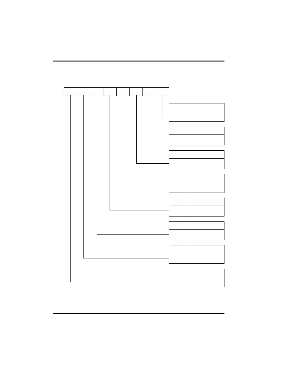
5 - 10
SMRR0 Mode Register
KR07
KR06
KR05
KR04
KR03
KR02
KR01
KR00
SMRR0
W <00DCH>
7
0
KR00
Key Input Selection
0
1
no select
select
KR01
Key Input Selection
0
1
no select
select
KR02
Key Input Selection
0
1
no select
select
KR03
Key Input Selection
0
1
no select
select
KR04
Key Input Selection
0
1
no select
select
KR05
Key Input Selection
0
1
no select
select
KR06
Key Input Selection
0
1
no select
select
KR07
Key Input Selection
0
1
no select
select
Chapter 5. Interrupt

5 - 11
SMRR1 Mode Register
KR17
KR16
KR15
KR14
KR13
KR12
KR11
KR10
SMRR1
W <00DDH>
7
0
KR10
Key Input Selection
0
1
no select
select
KR11
Key Input Selection
0
1
no select
select
KR12
Key Input Selection
0
1
no select
select
KR13
Key Input Selection
0
1
no select
select
KR14
Key Input Selection
0
1
no select
select
KR15
Key Input Selection
0
1
no select
select
KR16
Key Input Selection
0
1
no select
select
KR17
Key Input Selection
0
1
no select
select
Chapter 5. Interrupt

OVERVIEW
1
FUNCTION DESCRIPTION
2
I/O PORT
3
PERIPHERAL HARDWARE
4
INTERRUPT
5
STANDBY FUNCTION
6
RESET FUNCTION
7
APPENDIX A.
8
APPENDIX B.
9

6 - 1
CHAPTER 6. STANDBY FUNCTION
To save power consumption, there is STOP modes. In this modes, the execution of
program stops.
6.1 STOP MODE
STOP mode can be entered by STOP instruction during program. In STOP mode,
oscillator is stopped to make all clocks stop, which leads to less power consumption. All
registers and RAM data are preserved.
°»
NOP
°»
instruction should be follows STOP
instruction for rising precharge time of Data Bus line.
ex) STOP : STOP instructiion excution
NOP : NOP instruction
Chapter6. Standby Function

6 - 2
Selector
Prescaler
ENPCK
Basic Interval Timer
PS10
Peripheral
Fig. 6.2 ENPCK and Basic Interval Timer Clock
Fig. 6.1 Block Diagram of Standby Circuit
Chapter6. Standby Function
OSC.
Circuit
Clock Pulse GEN
CLR
MUX
Prescaler
CLR
S Q
R
S Q
R
Overflow Detection
Basic Interval Timer
CLR
CPU Clock
B.I.T 7
STOP
Release Signal From Interrupt Circuit
RESET
Control
Signal

6 - 3
6.2 STANDBY MODE RELEASE
6.2.1 STOP Mode Release
Release of STANDBY mode is executed by RESET input and Interrupt signal. Register
value is defined when Reset. When there is a release signal of STOP mode (Interrupt,
RESET input), the instruction execution starts after stabilization oscillation time is set by
value of BTS2~BTS0 and set ENPCK to 1.
Table 6.1. Standby Mode Register
Release Signal
STOP
RESET
0
KSCN (Key input)
0
INT1 - INT2
0
Table 6.2 Standby Mode Release
Release Factor
Release Method
RESET Pin
By RESET Pin = Low level, Standby mode is release and system is initialized
KSCN
(Key input)
Standby mode is released by Low input of selected pin by Key Scan Input
(SMRR0, SMRR1)
In case of interrupt Mask Enable flag = 0, program executes just after standby
instruction, if flag = 1, enters each interrupt service routine.
INT 1 pin
INT 2 pin
When external interrupt (INT1, INT2) enable flag is
°»
1
°»
, standby mode is
released at the rising edge of each terminal.
When Standby mode is released at interrupt. Mask Enable flag = 0, program
executes from the next instruction of standby instruction.
When 1, enters each interrupt service routine.
Chapter6. Standby Function

6 - 4
<STOP MODE>
STOP Mode
Stable
OSC. time
Program Setting Time by CKCTLR
Refer to Table 4-1
Longer than stable OSC. Time
CLCOK
Release By Interrupt
RESET
Fig. 6.3 Release Timing of Standby Mode
6.3 RELEASE OPERATION OF STANDBY MODE
After Standby mode is released, the operation begins according to content of
related interrupt register just before Standby mode start(Fig. 6.3)
6.3.1 In Case of Interrupt Enable Flag(I) of PSW = 0
Release by only interrupt which interrupt enable flag = 1, and starts to execute from next
to Standby instruction (STOP).
Chapter6. Standby Function

6 - 5
6.3.2 In Case of Interrupt Enable Flag(I) of PSW = 1
Released by only interrupt which each interrupt enable flag = 1, and jump to the relevant
interrupt service routine.
Note) When STOP instruction is used, B.I.T should guarantee the stabilization oscillation
time. Thus, just before entering STOP mode, clock of bit10(PS10) of Prescaler is
selected or peripheral hardware clock control bit(ENPCK) to 1, Therefore the clock
necessary for stabilization oscillation time should be input into B.I.T. otherwise, Standby
mode is released by reset signal. In case of interrupt request flag and interrupt enable
flag are both
°»
1
°»
, Standby mode is not entered.
Fig. 6.5 Standby Mode Release Flow
STOP Command
Standby Mode
Interrupt Request GEN.
IE Flag
Standby Mode Release
PSW
IE Flag
Interrupt Service Routine
Standby Next Command
Execution
0
1
0
1
Chapter6. Standby Function

6 - 6
Internal circuit
STOP Mode
Oscillator
Stop
Internal CPU clock
Stop
Register
Retained
RAM
Retained
I/O port
Retained
Prescaler
Stop
Basic Interval Timer
Stop
Watch Dog Timer
Stop
Timer
Stop
Address Bus, Data Bus
Retained
Table 6.3 Operation State in Standby Mode
Chapter6. Standby Function

OVERVIEW
1
FUNCTION DESCRIPTION
2
I/O PORT
3
PERIPHERAL HARDWARE
4
INTERRUPT
5
STANDBY FUNCTION
6
RESET FUNCTION
7
APPENDIX A.
8
APPENDIX B.
9

7 - 1
CHAPTER 7. RESET FUNCTION
7.1 EXTERNAL RESET
The RESET pin should be held at low for at least 2machine cycles with the power supply
voltage within the operating voltage range and must be connected 0.1uF capacitor
for stable system initialization.
The RESET pin contains a Schmitt trigger with an internal pull-up resistor.
0.1uF capacitor
Fig 7.0 RESET Pin connection.
7.2 POWER ON RESET
Power On Reset circuit automatically detects the rise of power voltage (the rising time
should be within 50ms) the power voltage reaches a certain level, RESET terminal is
maintained at
°»
L
°»
Level until a crystal ceramic oscillator oscillates stably. After power
applies and starting of oscillation, this reset state is maintained for about oscillation cycle of
2
19
(about 65.5ms : at 4MHz).
The execution of built-in Power On Reset circuit is as follows :
(1) Latch the pulse from Power On Detection Pulse Generator circuit, and reset
Prescaler, B.I.T and B.I.T Overflow detection circuit.
(2) Once B.I.T Overflow detection circuit is reset. Then, Prescaler starts to count.
(3) Prescaler output is inputted into B.I.T and PS10 of Prescaler output is automatically
selected. If overflow of B.I.T is detected, Overflow detection circuit is set.
(4) Reset circuit generates maximum period of reset pulse from Prescaler and B.I.T.
Chapter7. Reset Function
RESET

7 - 2
Fig. 7.1 Block Diagram of Power On Reset Circuit
Notice ; When Power On Reset, oscillator stabilization time doesn`t include OSC. Start time.
Fig. 7.2 Oscillator stabilization diagram
RESET
Power On DET
Pulse GEN.
OSC.
CLR
Prescaler
CLR
Basic Interval
Tiemr
CLR
Basic Interval
Tiemr
XTAL
PS10
MSB
Internal Reset
Chapter7. Reset Function
VDD
OSC. START TIMING
PRESCALER COUNT START
VDD
VSS
0.1uF
Internal IC

7 - 3
RESET
ADDR. BUS
INTERNAL
DATA BUS
SP
SP-1
SP-2
FFFE
FFFF
NEW PC
FE
LSB
VECTOR
MSB
VECTOR
Fig. 7.3 Reset Timing by Diagram
Chapter7. Reset Function
INTERNAL
RESET

7 - 4
7.3 Low Voltage Detection Mode
7.3.1 Low voltage detection condition
An on board voltage comparator checks that V
DD
is at the required level to ensure
correct operation of the device. If V
DD
is below a certain level, Low voltage detector
forces the device into low voltage detection mode.
7.3.2 Low Voltage Detection Mode
There is no power consumption except stop current, stop mode release function is
disabled. All I/O port is configured as input mode and Data memory is retained until
voltage through external capacitor is worn out. In this mode, all port can be selected with
Pull-up resistor by Mask option. If there is no information on the Mask option sheet ,the
default pull up option (all port connect to pull-up resistor ) is selected.
7.3.3 Release of Low Voltage Detection Mode
Reset signal result from new battery(normally 3V) wakes the low voltage detection mode
and come into normal reset state. It depends on user whether to execute RAM clear
routine or not.
Chapter7. Reset Function
0.0
0.2
0.4
0.6
0.8
1.0
1.2
1.4
1.6
1.8
2.0
2.2
2.4
0
°…
10
°…
20
°…
30
°…
40
°…
50
°…
60
°…
70
°…
Temperature(°…)
Low Voltage (V)
2.6
2.8
3.0
Fig 7.5 Low Voltage vs Temperature

7 - 5
Chapter7. Reset Function
* SRAM BACK-UP after Low Voltage Detection.
3.0V
1.8V(TYP)
( 20°…)
* SRAM Data Backup
User
Removes
Batteries
User
Replace
Batteries
Interrupt
: disable
Stop release
: disable
All I/O port
: input Mode
Remout port
: Low Level
OSC
: STOP
All I/O port pull-up ON (Mask Option )
SRAM Data retention
* The operation after Low voltage detection
about hours depend on Vcc-Gnd Capacitor
0V
Low Voltage Detection
point
MCU OPR.
Voltage
Power On Reset
( SRAM unstable )
Power On Reset
( SRAM retention)
0.7V(V
RET
)
* S/W flow chart example after Reset using SRAM Back-up
RESET
Stack Pointer initialize
SRAM DATA IS VALID?
Check the SRAM value
(RAM Pattern, Check sum..)
N
Y
Clear All Ram area
Use saved SRAM
value

OVERVIEW
1
FUNCTION DESCRIPTION
2
I/O PORT
3
PERIPHERAL HARDWARE
4
INTERRUPT
5
STANDBY FUNCTION
6
RESET FUNCTION
7
APPENDIX A.
8
APPENDIX B.
9

A - 1
Appendix A. Instruction Set Table
APPENDIX A. INSTRUCTION SET TABLE
No.
MNEMONIC
OP CODE
Words
Exec.
Cycle
OPERATION
Flag
MVG HIZC
1
2
3
4
5
6
7
8
9
10
11
12
13
14
15
16
17
18
19
20
21
22
23
24
25
26
27
28
29
30
31
32
33
34
35
36
37
38
39
40
41
ADC
#imm
ADC
dp
ADC
dp+X
ADC
!abs
ADC
!abs+Y
ADC
[dp+X]
ADC
[dp]+Y
ADC
{X}
AND
#imm
AND
dp
AND
dp+X
AND
!abs
AND
!abs+Y
AND
[dp+X]
AND
[dp]+Y
AND
{X}
ASL
A
ASL
dp
ASL
dp+X
ASL
!abs
BBC
A.bit, rel
BBC
dp.bit, rel
BBS
A.bit, rel
BBS
dp.bit, rel
BCC
rel
BCS
rel
BEQ
rel
BIT
dp
BIT
!abs
BMI
rel
BNE
rel
BPL
rel
BRA
rel
BRK
BVC
rel
BVS
rel
CLR1
dp.bit
CLRA1
A.bit
CLRC
CLRG
CLRV
04
05
06
07
15
16
17
14
84
85
86
87
95
96
97
94
08
09
19
18
y2
y3
x2
x3
50
D0
F0
0C
1C
90
70
10
2F
0F
30
B0
y1
2B
20
40
80
2
2
2
3
3
2
2
1
2
2
2
3
3
2
2
1
1
2
2
3
2
3
2
3
2
2
2
2
3
2
2
2
2
1
2
2
2
2
1
1
1
2
3
4
4
5
6
6
3
2
3
4
4
5
6
6
3
2
4
5
5
4/6
5/7
4/6
5/7
2/4
2/4
2/4
4
5
2/4
2/4
2/4
4
8
2/4
2/4
4
2
2
2
2
A = A + op + C
°»
°»
°»
°»
°»
°»
°»
A = A & op
°»
°»
°»
°»
°»
°»
°»
op = op << 1
°»
°»
°»
if (bit = 0)
then branch
if (bit = 1)
then branch
if (C=0) branch
if (C=1) branch
if (Z=1) branch
Z = A & op
°»
if (N=1) branch
if (Z=0) branch
if (N=0) branch
Branch
S/W interrupt
if (V=0) branch
if (V=1) branch
op.bit = 0
°»
C = 0
G = 0
V = 0
N V . . H . Z C
N V . . H . Z C
N V . . H . Z C
N V . . H . Z C
N V . . H . Z C
N V . . H . Z C
N V . . H . Z C
N V . . H . Z C
N . . . . . Z .
N . . . . . Z .
N . . . . . Z .
N . . . . . Z .
N . . . . . Z .
N . . . . . Z .
N . . . . . Z .
N . . . . . Z .
N . . . . . Z C
N . . . . . Z C
N . . . . . Z C
N . . . . . Z C
. . . . . . . .
. . . . . . . .
. . . . . . . .
. . . . . . . .
. . . . . . . .
. . . . . . . .
. . . . . . . .
N N . . . . Z .
N N . . . . Z .
. . . . . . . .
. . . . . . . .
. . . . . . . .
. . . . . . . .
. . . 1 . 0 . .
. . . . . . . .
. . . . . . . .
. . . . . . . .
. . . . . . . .
. . . . . . . 0
. . 0 . . . . .
. 0 . . 0 . . .

A - 2
No.
MNEMONIC
OP CODE
Words
Exec.
Cycle
OPERATION
Flag
MVG HIZC
42
43
44
45
46
47
48
49
50
51
52
53
54
55
56
57
58
59
60
61
62
63
64
65
66
67
68
69
70
71
72
73
74
75
76
77
78
79
80
81
82
83
84
85
86
87
88
CMP
#imm
CMP
dp
CMP
dp+X
CMP
!abs
CMP
!abs+Y
CMP
[dp+X]
CMP
[dp]+Y
CMP
{X}
COM
dp
CMPX
#imm
CMPX
dp
CMPX
!abs
CMPY
#imm
CMPY
dp
CMPY
!abs
DAA
DAS
DEC
A
DEC
dp
DEC
dp + X
DEC
!abs
DEC
X
DEC
Y
DIV
DI
EI
EOR
#imm
EOR
dp
EOR
dp+X
EOR
!abs
EOR
!abs+Y
EOR
[dp+X]
EOR
[dp]+Y
EOR
{X}
INC
A
INC
dp
INC
dp + X
INC
!abs
INC
X
INC
Y
JMP
!abs
JMP
[!abs]
JMP
[dp]
CALL
!abs
CALL
[dp]
PCALL
upage
TCALL
n
44
45
46
47
55
56
57
54
2C
5E
6C
7C
7E
8C
9C
DF
CF
A8
A9
B9
B8
AF
BE
9B
60
E0
A4
A5
A6
A7
B5
B6
B7
B4
88
89
99
98
8F
9E
1B
1F
3F
3B
5F
4F
nA
2
2
2
3
3
2
2
1
2
2
2
3
2
2
3
1
1
1
2
2
3
1
1
1
1
1
2
2
2
3
3
2
2
1
1
2
2
3
1
1
3
3
2
3
2
2
1
2
3
4
4
5
6
6
3
4
2
3
4
2
3
4
3
3
2
4
5
5
2
2
12
3
3
2
3
4
4
5
6
6
3
2
4
5
5
2
2
3
5
4
8
8
6
8
Compare A, op
°»
°»
°»
°»
°»
°»
°»
dp = dp
Compare X, op
°»
°»
Compare Y, op
°»
°»
°»
Dec. adjustment (Add)
Dec. adjustment (Sub)
op = op -1
°»
°»
°»
°»
°»
Q:A, R:Y
°Á
YA/X
I = 0
I = 1
A = A + op
°»
°»
°»
°»
°»
°»
°»
OP = OP + 1
°»
°»
°»
°»
°»
Branch
°»
°»
Subroutine call
°»
°»
°»
N . . . . . Z C
N . . . . . Z C
N . . . . . Z C
N . . . . . Z C
N . . . . . Z C
N . . . . . Z C
N . . . . . Z C
N . . . . . Z C
N . . . . . Z .
N . . . . . Z C
N . . . . . Z C
N . . . . . Z C
N . . . . . Z C
N . . . . . Z C
N . . . . . Z C
N . . . . . Z C
N . . . . . Z C
N . . . . . Z C
N . . . . . Z C
N . . . . . Z C
N . . . . . Z C
N . . . . . Z C
N . . . . . Z C
N V . . H . Z .
. . . . . 0 . .
. . . . . 1 . .
N . . . . . Z .
N . . . . . Z .
N . . . . . Z .
N . . . . . Z .
N . . . . . Z .
N . . . . . Z .
N . . . . . Z .
N . . . . . Z .
N . . . . . Z C
N . . . . . Z C
N . . . . . Z C
N . . . . . Z C
N . . . . . Z C
N . . . . . Z C
. . . . . . . .
. . . . . . . .
. . . . . . . .
. . . . . . . .
. . . . . . . .
. . . . . . . .
. . . . . . . .
Appendix A. Instruction Set Table

A - 3
No.
MNEMONIC
OP CODE
Words
Exec.
Cycle
OPERATION
Flag
MVG HIZC
89
90
91
92
93
94
95
96
97
98
99
100
101
102
103
104
105
106
107
108
109
110
111
112
113
114
115
116
117
118
119
120
121
122
123
124
125
126
127
128
129
130
131
132
133
134
135
136
LDA
#imm
LDA
dp
LDA
dp+X
LDA
!abs
LDA
!abs+Y
LDA
[dp+X]
LDA
[dp]+Y
LDA
{X}
LDA
{X}+
LDM
dp, #imm
LDX
#imm
LDX
dp
LDX
dp+Y
LDX
!abs
LDY
#imm
LDY
dp
LDY
dp+X
LDY
!abs
LSR
A
LSR
dp
LSR
dp + X
LSR
!abs
MUL
NOP
OR
#imm
OR
dp
OR
dp+X
OR
!abs
OR
!abs+Y
OR
[dp+X]
OR
[dp]+Y
OR
{X}
PUSH
A
PUSH
X
PUSH
Y
PUSH
PSW
POP
A
POP
X
POP
Y
POP
PSW
ROL
A
ROL
dp
ROL
dp+X
ROL
!abs
ROR
A
ROR
dp
ROR
dp+X
ROR
!abs
C4
C5
C6
C7
D5
D6
D7
D4
DB
E4
1E
CC
CD
DC
3E
C9
D9
D8
48
49
59
58
5B
FF
64
65
66
67
75
76
77
74
0E
2E
4E
6E
0D
2D
4D
6D
28
29
39
38
68
69
79
78
2
2
2
3
3
2
2
1
1
3
2
2
2
3
2
2
2
3
1
2
2
3
1
1
2
2
2
3
3
2
2
1
1
1
1
1
1
1
1
1
1
2
2
3
1
2
2
3
2
3
4
4
5
6
6
3
4
5
2
3
4
4
2
3
4
4
2
4
5
5
9
2
2
3
4
4
5
6
6
3
4
4
4
4
4
4
4
4
2
4
5
5
2
4
5
5
A = op
°»
°»
°»
°»
°»
°»
°»
A = op, X = X+1
dp = #imm
X = op
°»
°»
°»
Y = op
°»
°»
°»
op = op >>1
°»
°»
°»
YA = Y * A
No operation
A = A : op
°»
°»
°»
°»
°»
°»
°»
Push op, SP = SP - 1
°»
°»
°»
Pop op, SP = SP + 1
°»
°»
°»
op = op << 1, with C
°»
°»
°»
op = op >> 1, with C
°»
°»
°»
N . . . . . Z .
N . . . . . Z .
N . . . . . Z .
N . . . . . Z .
N . . . . . Z .
N . . . . . Z .
N . . . . . Z .
N . . . . . Z .
N . . . . . Z .
. . . . . . . .
N . . . . . Z .
N . . . . . Z .
N . . . . . Z .
N . . . . . Z .
N . . . . . Z .
N . . . . . Z .
N . . . . . Z .
N . . . . . Z .
N . . . . . Z C
N . . . . . Z C
N . . . . . Z C
N . . . . . Z C
N . . . . . Z .
. . . . . . . .
N . . . . . Z .
N . . . . . Z .
N . . . . . Z .
N . . . . . Z .
N . . . . . Z .
N . . . . . Z .
N . . . . . Z .
N . . . . . Z .
. . . . . . . .
. . . . . . . .
. . . . . . . .
. . . . . . . .
. . . . . . . .
. . . . . . . .
. . . . . . . .
(restored)
N . . . . . Z C
N . . . . . Z C
N . . . . . Z C
N . . . . . Z C
N . . . . . Z C
N . . . . . Z C
N . . . . . Z C
N . . . . . Z C
Appendix A. Instruction Set Table

A - 4
No.
MNEMONIC
OP CODE
Words
Exec.
Cycle
OPERATION
Flag
MVG HIZC
137
138
139
140
141
142
143
144
145
146
147
148
149
150
151
152
153
154
155
156
157
158
159
160
161
162
163
164
165
166
167
168
169
170
171
172
173
174
175
176
177
178
179
RETI
RET
SBC
#imm
SBC
dp
SBC
dp+X
SBC
!abs
SBC
!abs+Y
SBC
[dp+X]
SBC
[dp]+Y
SBC
{X}
SETI
dp.bit
SETA1
A.bit
SETC
SETG
STA
dp
STA
dp+X
STA
!abs
STA
!abs+Y
STA
[dp+X]
STA
[dp]+Y
STA
{X}
STA
{X}+
STOP
STX
dp
STX
dp+Y
STX
!abs
STY
dp
STY
dp+X
STY
!abs
TAX
TAY
TST
dp
TSPX
TXA
TXSP
TYA
XAX
XAY
XCN
XMA
dp
XMA
dp+X
XMA
{X}
XYX
7F
6F
24
25
26
27
35
36
37
34
x1
0B
A0
C0
E5
E6
E7
F5
F6
F7
F4
FB
EF
EC
ED
FC
E9
F9
F8
E8
9F
4C
AE
C8
8E
BF
EE
DE
CE
BC
AD
BB
FE
1
1
2
2
2
3
3
2
2
1
2
2
1
1
2
2
3
3
2
2
1
1
1
2
2
3
2
2
3
1
1
2
1
1
1
1
1
1
1
2
2
1
1
6
5
2
3
4
4
5
6
6
3
4
2
2
2
4
5
5
6
7
7
4
4
3
4
5
5
4
5
5
2
2
3
2
2
2
2
4
4
5
5
6
5
4
Interrupt end
Subroutine end
A = A - op - C
°»
°»
°»
°»
°»
°»
°»
op.bit = 1
°»
C = 1
G = 1
op = A
°»
°»
°»
°»
°»
°»
op = A, X=X+1
CPU, OSC stop
op = X
°»
°»
op = Y
°»
°»
X= A
Y = A
Test dp = 0 or not
X = SP
A = X
SP = X
A = Y
A
°Í
X
A
°Í
Y
A7-4 A3-0
A
°Í
op
°»
°»
X
°Í
Y
(restored)
. . . . . . . .
N V . . H . Z C
N V . . H . Z C
N V . . H . Z C
N V . . H . Z C
N V . . H . Z C
N V . . H . Z C
N V . . H . Z C
N V . . H . Z C
. . . . . . . .
. . . . . . . .
. . . . . . . 1
. . 1 . . . . .
. . . . . . . .
. . . . . . . .
. . . . . . . .
. . . . . . . .
. . . . . . . .
. . . . . . . .
. . . . . . . .
. . . . . . . .
. . . . . . . .
. . . . . . . .
. . . . . . . .
. . . . . . . .
. . . . . . . .
. . . . . . . .
. . . . . . . .
N . . . . . Z .
N . . . . . Z .
N . . . . . Z .
N . . . . . Z .
N . . . . . Z .
. . . . . . . .
N . . . . . Z .
. . . . . . . .
. . . . . . . .
N . . . . . Z .
N . . . . . Z .
N . . . . . Z .
N . . . . . Z .
. . . . . . .
Appendix A. Instruction Set Table

A - 5
No.
MNEMONIC
OP CODE
Words
Exec.
Cycle
OPERATION
Flag
MVG HIZC
180
181
182
183
184
185
186
187
188
189
190
191
192
193
194
195
196
197
198
199
200
201
202
LDYA
dp
STYA
dp
INCW
dp
DECW
dp
ADDW
dp
SUBW
dp
CMPW
dp
CBNE
dp, rel
CBNE
dp+X, rel
DBNE
dp, rel
DBNE
Y, rel
NOT1
M.bit
OR1
M.bit
OR1B
M.bit
AND1
M.bit
AND1B
M.bit
EOR1
M.bit
EOR1B
M.bit
LDC
M.bit
LDCB
M.bit
STC
M.bit
TCLR1
!abs
TSET1
!abs
7D
DD
9D
BD
1D
3D
5D
FD
8D
AC
7B
4B
6B
6B
8B
8B
AB
AB
CB
CB
EB
5C
3C
2
2
2
2
2
2
2
3
3
3
2
3
3
3
3
3
3
3
3
3
3
3
3
5
5
6
6
5
5
4
5/7
6/8
5/7
4/6
5
5
5
4
4
5
5
4
4
6
6
6
YA = (dp+1)(dp)
(dp+1)(dp) = YA
(dp+1)(dp)++
(dp+1)(dp)--
YA + (dp+1)(dp)
YA - (dp+1)(dp)
CP YA, (dp+1)(dp)
if (op !=A)
then branch
Dec op, if (Z=0)
then branch
M.bit = M.bit
C = M.bit : C
C = (M.bit) : C
C = M.bit & C
C = (M.bit) & C
C= M.bit + C
C = (M.bit) + C
C = M.bit
C = (M.bit)
M.bit = C
!abs = A & !abs
!abs = A : !abs
N . . . . . Z .
. . . . . . . .
N . . . . . Z .
N . . . . . Z .
N V . . H . Z C
N V . . H . Z C
N . . . . . Z C
. . . . . . . .
. . . . . . . .
. . . . . . . .
. . . . . . . .
. . . . . . . .
. . . . . . . C
. . . . . . . C
. . . . . . . C
. . . . . . . C
. . . . . . . C
. . . . . . . C
. . . . . . . C
. . . . . . . C
. . . . . . . .
N . . . . . Z .
N . . . . . Z .
Appendix A. Instruction Set Table

OVERVIEW
1
FUNCTION DESCRIPTION
2
I/O PORT
3
PERIPHERAL HARDWARE
4
INTERRUPT
5
STANDBY FUNCTION
6
RESET FUNCTION
7
APPENDIX A.
8
APPENDIX B.
9

B - 1
Appendix B. PROGRAMMER`S GUIDE
APPENDIX B.
General Circuit Diagram of GMS810series.
KEY MATRIX
= KEY
17
9
1
18
10
2
19
11
3
20
12
4
21
13
5
22
14
6
23
15
7
24
16
8
25
26
27
28
29
30
31
32
33
34
35
36
37
38
39
40
41
42
43
44
45
46
47
48
R15
R14
R13
R12
R11
R10
R00
R01
R02
R03
R04
R05
R06
R07
49
50
51
52
53
54
55
56
R16
OSC
R13
R14
R12
R15
R11
R16
R10
R17
VDD REMOUT
Xout RESET
Xin TEST
R00
R07
R01
R06
R02
R05
R03
R04
R20
VSS
TR1
GMS 81016
1
2
3
4
5
6
7
8
9
10
24
23
22
21
20
19
18
17
16
15
VCC
GND
14
13
11
12
0.1uF
220uF
0.1uF
DC3V
Indicator LED
VCC
VCC
B-1 Circuit Diagram
vcc
Infrared LED
4MHz
Normally use the above 100uF
capacitor for prevent power drop
during pulse is transmitted.
If you use the SRAM back-up,
use at least 220uF
We recommend to
use ALKALINE battery.
Filter for Vcc-GND
noise

B - 2
GMS810 MASK OPTION LIST
HYUNDAI ELCTRONICS Co., Ltd.
MCU Application Team.
Code Name : GMS81016 - UAxxx
1. Device & Package
Please enter check marks as
2. Inclusion of Pull up Resistor
- R1 PORT
Y : Yes
N : No
- R2 PORT
Date :
Company Name :
Section Name :
Signature :
24PIN : SOP Skinny DIP
28PIN : SOP
Skinny DIP
Y : Yes
N : No
- R0 PORT
Y : Yes
N : No
20PIN : SOP PDIP
< NOTICE >
. *0 : is only available in Low Voltage detection Option = Y (No . 3)
*1 : is not available for 20PIN & 24PIN. So, Default option is Pull-Up.
. *2 : is not available for 20PIN. So, Default Option is Pull-Up.
GMS81008
GMS81016
GMS81004
GMS81032
GMS81024
44PIN : PLCC
3. Low Voltage Detection
Y/N
n
Port
R00
Y/N
y
Y/N
*0
R01
y
R02
y
R03
y
R04
y
R05
y
R06
y
R07
y
Port
R10
Y/N
n
Y/N
*0
R11
n
R12*2
n
R13*2
n
R14*2
n
R15*2
n
R16
n
R17
n
Port
R20
Y/N
n
Y/N
*0
R21*1 R22*1 R23*1 R24*1
Mask Option List Example Refer to Circuit B-1
B-1 ,Circuit Description:
device : GMS81016
package : 24PIN SOP
port R0x : All input port with pull-up resistor
port R1x : All output port with N-MOS
Open drain
port R20 : LED Drive port
; Example program for Port setting.
ORG 0C000H ; GMS81016 Program Start Address
Reset :
clrg ; Clear G-Flag
ldx #0feh ; Stack Pointer Initialize
txsp
DI ; Interrupt disable
ldm R2dd,#0001_1111b ; R2 direction setting,R20: Output
ldm R2,#1111_1111b ; R2 data setting , R20 : High,Led off
ldm R1odc,#1111_1111b ; R1 port all open drain
ldm R1dd,#1111_1111b ; R1 direction setting ,All output
ldm R1,#0000_0000b ; R1 data setting , all Low for key scan
ldm R0dd,#0000_0000b ; R0 direction setting ,All input
ldm smrr0,#1111_1111b ; Stop mode release by R0
ldm smrr1,#0000_0000b ; Stop disable by R1
ldm Ienh,#1000_0000b ; Key scan interrupt setting
ldm ckctlr,#0001_1101b ; Ckctlr setting for 16mS time delay after
; release from stop mode, WDT disable.
clr1 IRQKSCN ; key scan interrupt request flag clear
STOP
NOP ; `NOP instruction must to be used after
ldm R1,#1111_1111b ; Stop instruction
S/W example Refer to Circuit B-1
Appendix B. PROGRAMMER`S GUIDE

B - 3
Appendix B. PROGRAMMER`S GUIDE
Key Scan
- To secure the key board scanning , read the input port after minimum 60uS delay time from
output port set to `Low `. This time delay is for the port rising time depend on the
input pull-up resistor .
; program example ,See the circuit B-1
.
ldm R1,#1111_1110b
;R10 port set to LOW
call delay_60uS
;60uS time delay routine
lda R0
;R0 port Read
.
.
R10
R11
60uS
60uS
R0 port Read timing
Fig B-2 , Input with pull-up port read time method

GMS810 MASK OPTION LIST
HYUNDAI ELECTRONICS Co., Ltd.
MCU Application Team.
Code Name :
1. Device & Package
Please enter check marks as
2. Inclusion of Pull up Resistor
- R1 PORT
Y : Yes
N : No
- R2 PORT
Date :
Company Name :
Section Name :
Signature :
24PIN : SOP Skinny DIP
28PIN : SOP
Skinny DIP
Y : Yes
N : No
- R0 PORT
Y : Yes
N : No
20PIN : SOP PDIP
< NOTICE >
. *0 : is only available in .Low Voltage detection Option = Y ( No. 3 )
*1 : is not available for 20PIN & 24PIN. So, Default Option is Pull-Up.
. *2 : is not available for 20PIN. So Default Option is Pull-Up.
GMS81008
GMS81016
GMS81004
GMS81032
GMS81024
44PIN : PLCC
3. Low Voltage Detection
R04
R05
R06
R07
Port
R00
R01
R02
R03
Y/N
Y/N
R14
R15
R16
R17
Port
R10
R11
R12
R13
Y/N
Y/N
*2 *2 *2 *2
R24
Port
R20
R21
R22
R23
Y/N
Y/N
*1 *1 *1
*1
Y/N
*0
*0
*0

0$6. 25'(5 9(5,),&$7,21 6+((7
*06
520 &2'( 1R
&XVWRPHU ,QIRUPDWLRQ
'HYLFH ,QIRUPDWLRQ
&RPSDQ\ 1DPH
$SSOLFDWLRQ
2UGHU 'DWH
7(/
)$;
1DPH
6LJQDWXUH
3DFNDJH
)LOH 1DPH
&KHFN 6XP
0D
V
N
'D
WD
'LVN
(0DLO
�
0DUNLQJ 6SHFLILFDWLRQ
'HOLYHU\ 6FKHGXOH
'DWH
&XVWRPHU 6DPSOH
5LVN 2UGHU
4XDQWLW\
SFV
SFV
+(, &RQILUPDWLRQ
520 &2'( 9HULILFDWLRQ
1DPH
6LJQDWXUH
9HULILFDWLRQ 'DWH
3OHDVH FRQILUP RXU YHULILFDWLRQ GDWD
&KHFN 6XP
7(/
)$;
$SSURYDO 'DWH
, DJUHH ZLWK \RXU YHULILFDWLRQ GDWD DQG FRQILUP
\RX WR PDNH PDVN VHW
7(/
)$;
1DPH
6LJQDWXUH
+<81'$, (OHFWURQLFV ZULWH LQ EHORZ
&XVWRPHU ZULWH LQ EHORZ
&
273
8
$
< < ::
. 2 5 ( $
+<81'$,
&XVWRPHU SDUW 1XPEHU
8
$
< < ::
. 2 5 ( $
&XVWRPHU /RJR
&XVWRPHU SDUW 1XPEHU
6.',3
623
623
623
6HW ))K LQ WKH XQXVHG DUHD
3',3
6.',3
3/&&
5HPRWH FRQWUROOHU
K
HYUNDAI Electronics Industrial