/home/web/htmldatasheet/RUSSIAN/html/hynix/213015

8-BIT SINGLE-CHIP MICROCONTROLLERS
GMS87C4060
GMS81C4040
User's Manual
MicroElectronics
Semiconductor Group of Hyundai Electronics Industrial Co., Ltd.

Additional information of this manual may be served by HYUNDAI Micro Electronics offices in Korea or Dis-
tributors and Representatives listed at address directory.
HYUNDAI Micro Electronics reserves the right to make changes to any information here in at any time without
notice.
The information, diagrams and other data in this manual are correct and reliable; however, HYUNDAI Micro
Electronics is in no way responsible for any violations of patents or other rights of the third party generated by
the use of this manual.
Version 1.00
Published by
MCU Application Team bjlim@hmec.co.kr conner@hmec.co.kr
2000 HYUNDAI Micro Electronics All right reserved.

HYUNDAI
GMS81C4040/87C4060
May. 2000 Ver 1.0
1
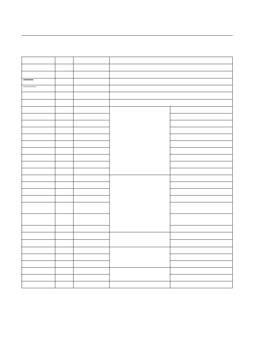
Table of Contents
OVERVIEW.......................................... 1
Description ...................................................1
Features .......................................................1
Development Tools..................................... 2
BLOCK DIAGRAM .............................. 3
PIN ASSIGNMENT .............................. 4
PACKAGE DIAGRAM ......................... 5
PIN FUNCTION .................................... 6
PORT STRUCTURES .......................... 9
RESET ................................................................ 9
TEST ................................................................... 9
XIN, XOUT ........................................................ 9
OSC1, OSC2 ..................................................... 9
R00~07, R53 ...................................................... 9
R10~15 (AN0~5) ................................................ 9
R16, 17, 20, 24, 25, 26, 27, 52, 67 ................... 10
R21/Sclk, R22/Sout .......................................... 10
R23/Sin ............................................................ 10
R40~43 (PWM0~3) .......................................... 10
R44, 45, 46, 47 (SCL, SDA, PWM) .................. 10
R50/BUZZ, R51/PWM8 .................................... 11
R54/YM, R55/YS, R56/I ................................... 11
R, G, B ............................................................. 11
ELECTRICAL CHARACTERISTICS . 12
Absolute Maximum Ratings .....................12
Recommended Operating Conditions ....12
DC Electrical Characteristics - GMS81C4040
.....................................................................12
A/D Comparator Characteristics .............14
AC Characteristics ....................................14
Typical Characteristics ............................16
MEMORY ORGANIZATION .............. 17
Registers ...................................................17
Program Memory ......................................20
PCALL
rel ..................................................... 21
TCALL
n ....................................................... 21
Data Memory .............................................23
User Memory .................................................... 23
Control Registers ............................................. 23
Stack Area ........................................................ 23
Addressing Mode ......................................25
(1) Register Addressing ................................... 25
(2) Immediate Addressing
#imm .................. 25
(3) Direct Page Addressing
dp ..................... 25
(4) Absolute Addressing
!abs ....................... 25
(5) Indexed Addressing .................................... 26
X indexed direct page (no offset)
{X} ........... 26
X indexed direct page, auto increment
{X}+ . 26
X indexed direct page (8 bit offset)
dp+X ..... 26
Y indexed direct page (8 bit offset)
dp+Y ..... 27
Y indexed absolute
!abs+Y .......................... 27
Direct page indirect
[dp] ............................... 27
X indexed indirect
[dp+X] ............................. 27
Y indexed indirect
[dp]+Y ............................. 28
Absolute indirect
[!abs] ................................ 28
I/O PORTS ......................................... 29
Registers for Port ..................................... 29
Port Data Registers .......................................... 29
I/O Ports Configuration ............................ 30
R0 Ports ........................................................... 30
R1 Ports ........................................................... 30
R2 Port ............................................................. 31
R4 Port ............................................................. 31
R5 Port ............................................................. 32
R6 Port ............................................................. 32
CLOCK GENERATOR ...................... 33
TIMER ................................................ 34
Basic Interval Timer ................................. 34
Timer 0, 1 ................................................... 35
Timer / Event Counter 2, 3 ....................... 37
Timer Mode ...................................................... 39
Event counter Mode ......................................... 39
A/D Converter ................................... 42
Control .............................................................. 42
Serial I/O ........................................... 44
Control .............................................................. 44
Pulse Width Modulation (PWM) ...... 46
8bit PWM Control ............................................. 47
14bit PWM Control ........................................... 47
Interrupt interval measurement circuit
........................................................... 49
Control .............................................................. 49
Buzzer driver .................................... 51
Control .............................................................. 51
On Screen Display (OSD) ................ 53
OSDCON1 ....................................................... 55
OSDCON2 ....................................................... 55
OSDPOL .......................................................... 56
FDWSET .......................................................... 56
L1ATTR ............................................................ 57
L1VPOS ........................................................... 58
L2ATTR ............................................................ 58
L2VPOS ........................................................... 58
COLMOD ......................................................... 58
MESHCON ....................................................... 58
VRAM ............................................................... 58
Font ROM ......................................................... 60

GMS81C4040/87C4060
HYUNDAI
2
May. 2000 Ver 1.0
Sprite RAM ....................................................... 60
Test Font .......................................................... 61
I2C Bus Interface .............................. 62
Control .............................................................. 62
I2C address register ......................................... 62
I2C data shift register [ICDR] ........................... 63
I2C status register ............................................ 63
I2C control register 1 ........................................ 64
I2C control register 2 ........................................ 64
START condition generation ............................ 65
RESTART condition generation ....................... 65
STOP condition generation .............................. 65
START / STOP condition detect ...................... 66
Address data communication ........................... 67
INTERRUPTS .................................... 68
Interrupt Mode Register ................................... 68
Interrupt Sequence ...................................72
Interrupt acceptance ........................................ 72
Saving/Restoring General-purpose Register ... 73
Multi Interrupt ............................................74
External Interrupt ..................................... 75
Response Time ................................................ 75
WATCHDOG TIMER ......................... 76
Watchdog Timer Control .................................. 76
Enable and Disable Watchdog ......................... 77
Watchdog Timer Interrupt ................................ 77
Minimizing Current Consumption ..................... 78
OSCILLATOR CIRCUIT .................... 80
RESET ............................................... 81
External Reset Input ................................. 81
Watchdog Timer Reset ............................ 82
OTP Programming ........................... 83
GMS87C4060 OTP Programming ............ 83
.Device configuration data ...................... 84
Timing Chart ............................................. 87
Assemble mnemonics ..................... 89
Instruction Map ......................................... 89
Alphabetic order table of instruction ..... 90
Instruction Table by Function ................. 94
HYUNDAI
GMS81C4040/87C4060
May. 2000 Ver 1.0
1
GMS81C4040/GMS87C4060
CMOS SINGLE-CHIP 8-BIT MICROCONTROLLER
FOR TELEVISION
1. OVERVIEW
1.1 Description
The GMS81C4040/GMS87C4060 is an advanced CMOS 8-bit microcontroller with 40K(60K) bytes of ROM. The device is
one of GMS800 family. The HYUNDAI's GMS81C4040/GMS87C4060 is a powerful microcontroller which provides a
highly flexible and cost effective solution to many TV applications. The GMS81C4040/GMS87C4060 provides the follow-
ing standard features: 40K(60K) bytes of ROM, 1,536 bytes of RAM, 8-bit timer/counter .
1.2 Features
� 40K(60K) Bytes On-chip Program Memory
� 1,536 Bytes of On-chip Data RAM
(Included 256 bytes stack memory)
� Instruction Cycle Time (ex:NOP)
- 0.5us at 8MHz
� 40 Programmable I/O pins
- 33 I/O and 7 Output pins
� Serial I/O : 8bit x 1ch
� I
2
C Bus interface
- Multimaster (2 Pairs interface pins)
� A/D Converter : 8bit x 6ch (TBD LSB)
� Pulse Width Modulation
- 14bit x 1ch
- 8bit x 6ch
� Timer
- Timer/Counter : 8bit x 4ch (16bit x 2ch)
- Basic interval timer : 8bit x 1ch
- Watch Dog Timer
� Number of Interrupt sources : 18
� On Screen Display
- Number of characters : 512 (6 characters are
reserved for IC test)
- Character size : 12 dots(X) x 16 dots(Y)
- Character display size : Large, Medium, Small
- DIsplay capability : 24Characters x 16 Line
(Two line VRAM buffer)
- Character, Back ground color : 16kinds
- Special functions : Rounding, Outline, Sprite,
Shadow,...
� Buzzer Driving port
- 500Hz ~ 250kHz @8MHz (Duty 50%)
� Operating Range : 4.5V to 5.5V
Device name
ROM Size
RAM Size
Package
GMS81C4040
40K bytes
Mask ROM
1,536 bytes
52SDIP
GMS87C4060
60K bytes
EPROM
1,536 bytes
52SDIP

GMS81C4040/87C4060
HYUNDAI
2
May. 2000 Ver 1.0
1.3 Development Tools
The GMS81C4040/GMS87C4060 is supported by a full-
featured macro assembler / linker , OSD font editor, an in-
circuit emulator CHOICE-Dr
TM
.
In Circuit Emulators
CHOICE-Dr.
(with EVA81C4xxx board)
Assembler / Linker
HYUNDAI's Macro Assembler /
Linker
Font Editor
MS-Windows GUI version
Debugger
MS-Windows GUI version
HYUNDAI
GMS81C4040/87C4060
May. 2000 Ver 1.0
3
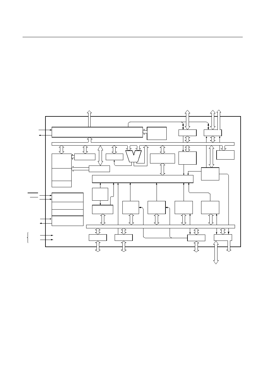
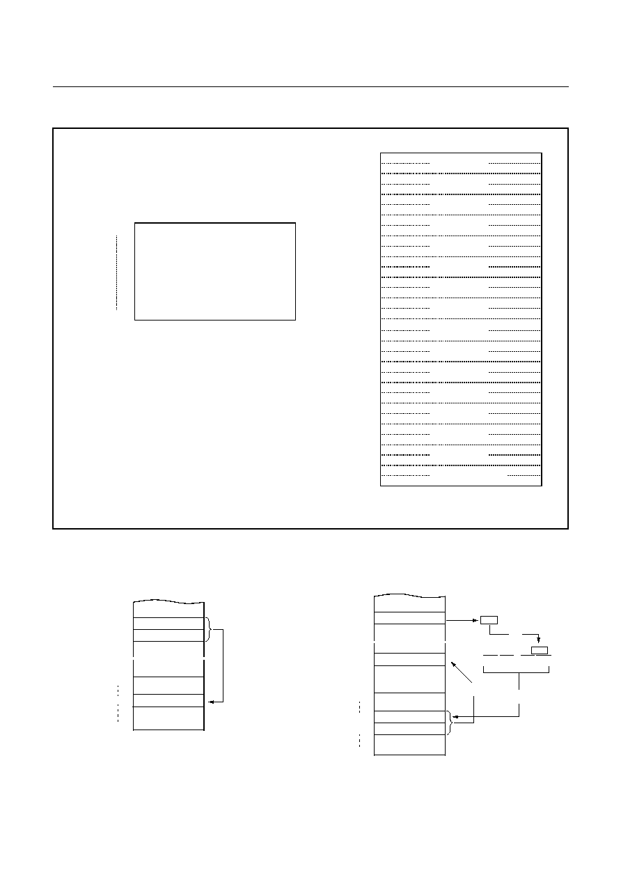
2. BLOCK DIAGRAM
ALU
OSD (On Screen Display) Controller
Accumulator
Interrupt Controller
Data
Memory
OSD
Memory
Display
8-bit x 4
Counter
Timer/
Program
Memory
Vector Table
8-bit Basic
Tim er
Interval
Watchdog
Timer
PSW
System controller
Timing generator
System
Clock Controller
RESET
TEST
XIN
XOUT
OSC1
OSC2
R,G,B
VDD
VSS
Power
Supply
R 1
Clock generator
& Index X,Y
8bit A/D
C on verto r
Buzzer
R 5
PWM
14 bit x 1
8b it x 6
D a t a b u s
I
2
C
In te rface
R 4
D a t a b u s
Serial I/O
In terfa ce
Interrupt
In te rva l
M ea sure
R 2
R 0
R 6
Stack pointer
PC
R00
R01
R02
R03
R04
R05
R06
R07
R67 / INT1
R20 / INT2
R21 / Sclk
R22 / Sout
R23 / Sin
R24 / INT3
R25 / EC2
R26 / INT4
R27 / EC3
R40 / PWM0
R41 / PWM1
R42 / PWM2
R43 / PWM3
R44 / SCL0
R45 / SCL1 / PWM4
R46 / SDA0
R47 / SDA1 / PWM5
R10 / AN0
R11 / AN1
R12 / AN2
R13 / AN3
R14 / AN4
R15 / AN5
R16 / VD
R17 / HD
R50 / BUZZ
R51 / PWM8
R52 / INT0
R53
R54 / YM
R55 / YS
R56 / I
GMS81C4040/87C4060
HYUNDAI
4
May. 2000 Ver 1.0
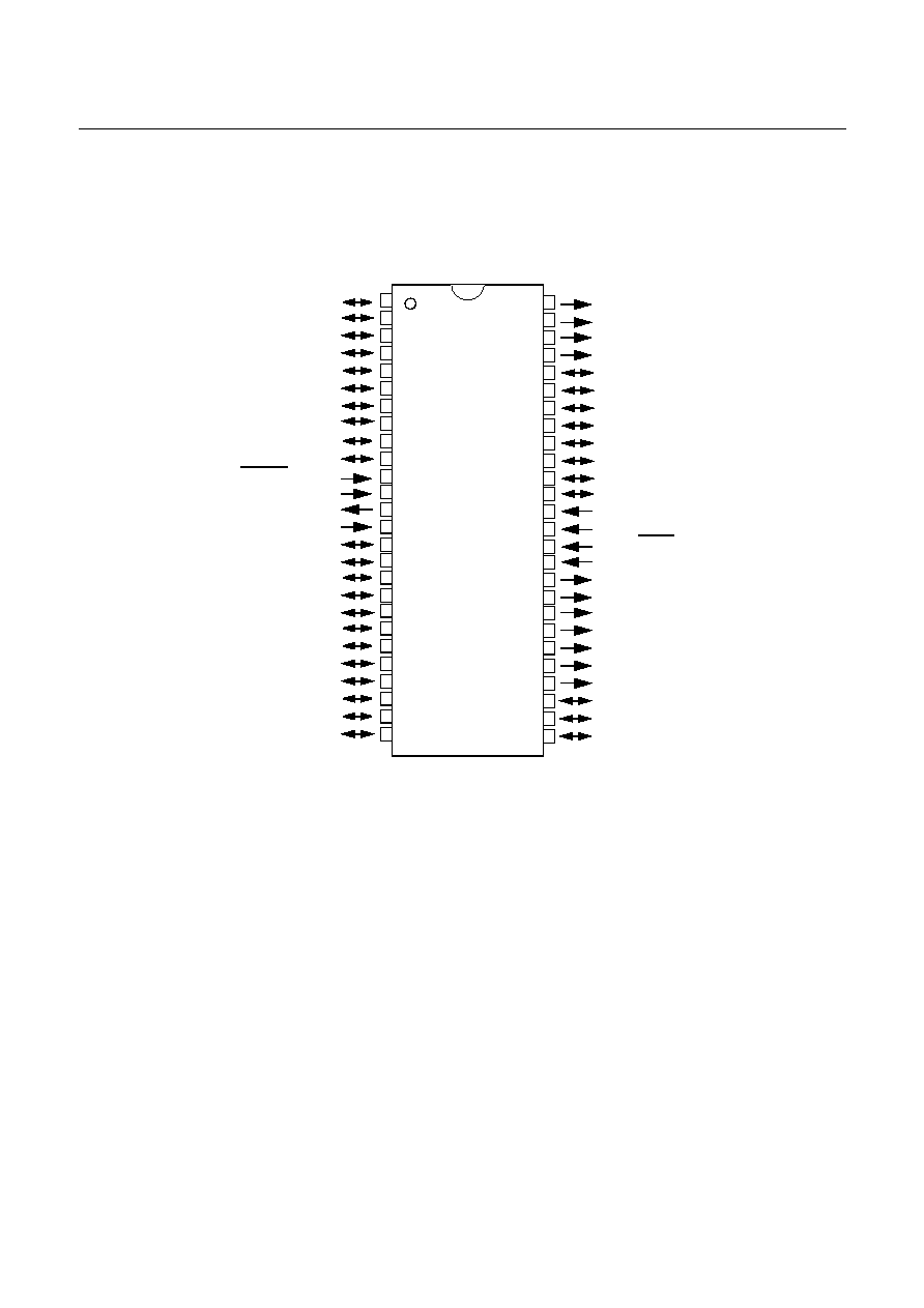
3. PIN ASSIGNMENT
R40/PWM0
R41/PWM1
R42/PWM2
R43/PWM3
R44/SCL0
R45/SCL1/PWM4
R46/SDA0
R47/SDA1/PWM5
R50/BUZZ
R51/PWM8
R52/INT0
R53
Vss
Vdd
TEST
OSC1
OSC2
R54/YM
R55/YS
R56/I
B
G
R
R00
R01
R02
R27/EC3
R26/INT4
R25/EC2
R24/INT3
R23/Sin
R22/Sout
R21/Sclk
R20/INT2
R17/HD
R16/VD
RESET
Vss
Xout
Xin
R15/AN5
R14/AN4
R13/AN3
R12/AN2
R11/AN1
R10/AN0
R07
R06
R05
R04
R03
R67/INT1
52
51
50
49
48
47
46
45
44
43
42
41
40
39
38
37
36
35
34
33
32
31
30
29
28
27
1
2
3
4
5
6
7
8
9
10
11
12
13
14
15
16
17
18
19
20
21
22
23
24
25
26
HY
UNDAI
GMS8
1C40
XX
HYUNDAI
GMS81C4040/87C4060
May. 2000 Ver 1.0
5
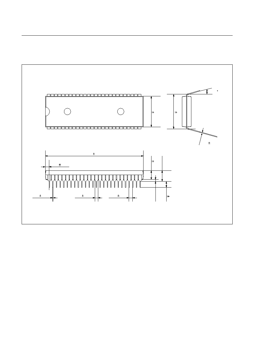
4. PACKAGE DIAGRAM
Figure 4-1 52pin Shrink DIP Package Diagram
UNIT: mm
HYUNDAI
GMS81C40XX
1
26
27
52
45.97
0.13
0.76
0.13
1.778
0.25
4.38
Max
.
13
.
9
7
0.
2
5
15
.
2
4
0.
2
5
0.47
0.13
1.02
0.25
3.81
0.
1
3
3.
2
4
0.20
0.50
Mi
n
.
0.25
0.05
0 ~ 15

GMS81C4040/87C4060
HYUNDAI
6
May. 2000 Ver 1.0
5. PIN FUNCTION
V
DD
: Supply voltage.
V
SS
: Circuit ground.
TEST: Used for shipping inspection of the IC. For normal
operation, it should not be connected .
RESET: Reset the MCU.
X
IN
: Input to the inverting oscillator amplifier and input to
the internal main clock operating circuit.
X
OUT
: Output from the inverting oscillator amplifier.
OSC1: Input to the internal On Screen Display operating
circuit.
OSC2: Output from the inverting OSC1 amplifier.
R00~R07: R0 is an 8-bit CMOS bidirectional I/O port. R0
pins 1 or 0 written to the Port Direction Register can be
used as outputs or inputs.
R10~R17: R1 is an 8-bit CMOS bidirectional I/O port. R1
pins 1 or 0 written to the Port Direction Register can be
used as outputs or inputs.
In addition, R1 serves the functions of the various follow-
ing special features.
R20~R27: R2 is a 8-bit CMOS bidirectional I/O port. Each
pins 1 or 0 written to the their Port Direction Register can
be used as outputs or inputs.
In addition, R2 serves the functions of the various follow-
ing special features.
R40~R47: R40~R43 are 8-bit NMOS open drain output
and R45~R47 are bidirectional CMOS Input / NMOS open
drain output port. R4 pins 1 or 0 written to the Port Direc-
tion Register can be used as outputs or inputs.
In addition, R4 serves the functions of the various follow-
ing special features.
R50~R56: R50~R53 are 4-bit CMOS bidirectional I/O and
R54~R56 are CMOS output port. R5 pins 1 or 0 written to
the Port Direction Register can be used as outputs or in-
puts.
In addition, R5 serves the functions of the various follow-
ing special features.
R67: R67 is an 1-bit CMOS bidirectional I/O port. R67
pins 1 or 0 written to the Port Direction Register can be
used as outputs or inputs.
In addition, R67 serves the functions of the various follow-
ing special features.
R,G,B: R,G,B CMOS output port. Each pins controls Red,
Green,. Blue color control.
Port pin
Alternate function
R10
R11
R12
R13
R14
R15
R16
R17
AN0 (A/D converter input 0)
AN1 (A/D converter input 1)
AN2 (A/D converter input 2)
AN3 (A/D converter input 3)
AN4 (A/D converter input 4)
AN5 (A/D converter input 5)
VD (Vertical Sync. input)
HD (Horisontal Sync. input)
Port pin
Alternate function
R20
R21
R22
R23
R24
R25
R26
R27
INT2 (External interrupt input 2)
Sclk (Serial communication clock)
Sout (Serial communication data out)
Sin (Serial communication data in)
INT3 (External interrupt input 3)
EC2 (Event counter input 2)
INT4 (External interrupt input 4)
EC3 (Event counter input 3)
Port pin
Alternate function
R40
R41
R42
R43
R44
R45
R46
R47
PWM0 (Pulse Width Modulation output 0)
PWM1 (Pulse Width Modulation output 1)
PWM2 (Pulse Width Modulation output 2)
PWM3 (Pulse Width Modulation output 3)
SCL0 (I
2
C Clock 0)
SCL1 (I
2
C Clock 1)
PWM4 (Pulse Width Modulation output 4)
SDA0 (I
2
C Data 0)
SDA1 (I
2
C Data 1)
PWM5 (Pulse Width Modulation output 5)
Port pin
Alternate function
R50
R51
R52
R54
R55
R56
BUZZ (Buzzer output)
PWM8 (Pulse Width Modulation output 8)
INT0 (External interrupt input 0)
YM (Back ground)
YS (Edge)
I (Intencity)
Port pin
Alternate function
R67
INT1 (External interrupt input 1)
HYUNDAI
GMS81C4040/87C4060
May. 2000 Ver 1.0
7
PIN NAME
Pin No.
In/Out
Function
V
DD
39
-
Supply voltage
V
SS
12, 40
-
Circuit ground
TEST
38
I
For test purposes. Should not be connected. (N.C.)
RESET
11
I
Reset signal input
X
IN
14
I
Main oscillation input
X
OUT
13
O
Main oscillation output
OSC1
37
I
On screen display functions
On screen display oscillation input
OSC2
36
O
On screen display osc. output
R17/HD
9
I/O
Horisontal Sync. input
R16/VD
10
I/O
Vertical Sync. input
R
30
O
Red signal output
G
31
O
Green signal output
B
32
O
Blue signal output
R56/I
33
O
Intencity signal output
R55/YS
34
O
Edge signal output
R54/YM
35
O
Background signal output
R40/PWM0
52
O
PWM functions
8bit PWM
R41/PWM1
51
O
8bit PWM
R42/PWM2
50
O
8bit PWM
R43/PWM3
49
O
8bit PWM
R45/SCL1/
PWM4
47
I/O
Include I
2
C Serial clock 1 (SCL1)
R47/SDA1/
PWM5
45
I/O
Include I
2
C Serial data 1 (SDA1)
R51/PWM8
43
I/O
14bit PWM
R44/SCL0
48
I/O
I
2
C functions
I
2
C Serial clock 0
R46/SDA0
46
I/O
I
2
C Serial data 0
R23/Sin
5
I/O
SCI functions
Serial data input
R22/Sout
6
I/O
Serial data output
R21/Sclk
7
I/O
Serial communication clock
R27/EC3
1
I/O
Timer event functions
Event counter input 3
R25/EC2
3
I/O
Event counter input 2
R50/Buzzer
44
I/O
Buzzer function
500Hz ~ 250KHz @8MHz
Table 5-1 Port Function Description
GMS81C4040/87C4060
HYUNDAI
8
May. 2000 Ver 1.0
R52/INT0
42
I/O
External interrupt functions
External interrupt input 0
R67/INT1
26
I/O
External interrupt input 1
R20/INT2
8
I/O
External interrupt input 2
R24/INT3
4
I/O
External interrupt input 3
R26/INT4
2
I/O
External interrupt input 4
R10/AN0
20
I/O
A/D conversion functions
Analog input 0
R11/AN1
19
I/O
Analog input 1
R12/AN2
18
I/O
Analog input 2
R13/AN3
17
I/O
Analog input 3
R14/AN4
16
I/O
Analog input 4
R15/AN5
15
I/O
Analog input 5
R00
29
I/O
Digital I/O functions
R01
28
I/O
R02
27
I/O
R03
25
I/O
R04
24
I/O
R05
23
I/O
R06
22
I/O
R07
21
I/O
R53
41
I/O
PIN NAME
Pin No.
In/Out
Function
Table 5-1 Port Function Description
HYUNDAI
GMS81C4040/87C4060
May. 2000 Ver 1.0
9
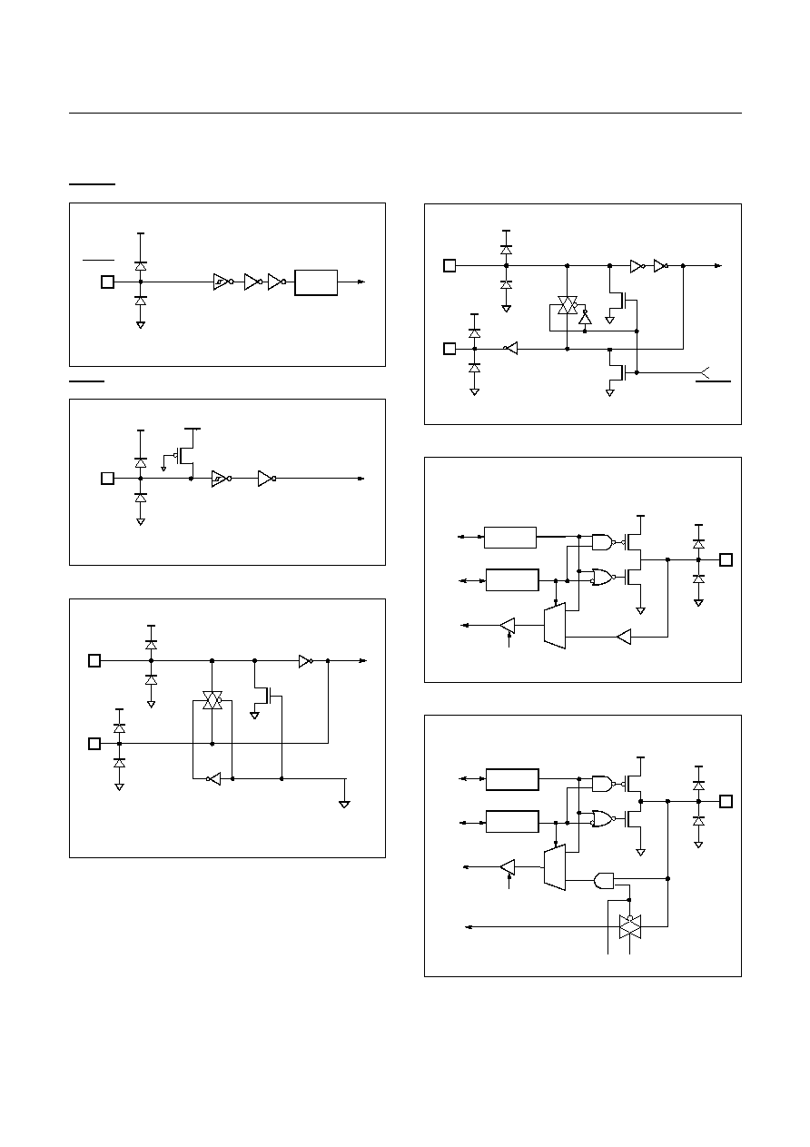
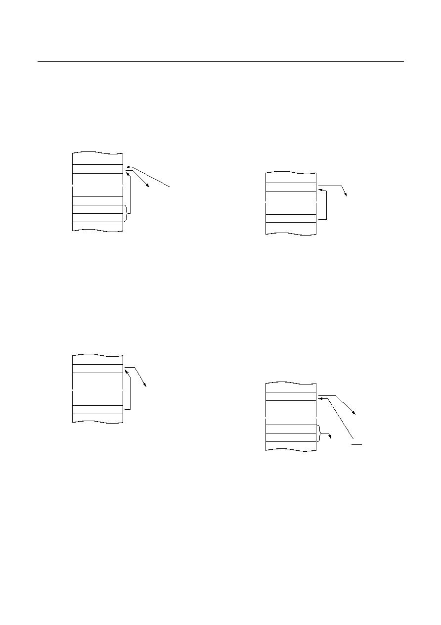
6. PORT STRUCTURES
RESET
TEST
X
IN
, X
OUT
OSC1, OSC2
R00~07, R53
R10~15 (AN0~5)
RESET
V
DD
V
SS
Noise
Canceler
V
DD
V
SS
X
IN
X
OUT
V
SS
V
DD
V
SS
V
DD
Main frequency
clock
V
S S
OSDON
OSC1
OSC2
V
SS
V
DD
V
SS
V
DD
Main frequency
clock
Pin
Data Reg.
Dir. Reg.
DB
DB
DB
MU X
RD
V
DD
V
SS
Pin
Data Reg.
Dir. Reg.
DB
DB
DB
MU X
RD
V
DD
V
SS
AN0~5
GMS81C4040/87C4060
HYUNDAI
10
May. 2000 Ver 1.0
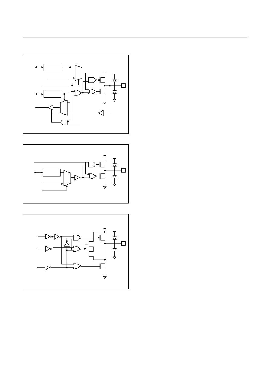
R16, 17, 20, 24, 25, 26, 27, 52, 67
R21/Sclk, R22/Sout
R23/Sin
R40~43 (PWM0~3)
R44, 45, 46, 47 (SCL, SDA, PWM)
Pin
Data Reg.
Dir. Reg.
DB
DB
DB
MU X
RD
V
DD
V
SS
HD,VD,
EC2~3
INT0~INT4
Pin
Data Reg.
Dir. Reg.
DB
DB
DB
M U X
RD
V
DD
V
SS
Sclk
M U X
Sout, Sclk
Selection
Pin
Data Reg.
Dir. Reg.
DB
DB
DB
M U X
RD
V
DD
V
SS
Sin
Selection
Pin
Data Reg.
DB
V
SS
M UX
PWM0~3
Selection
Pin
Data Reg.
Dir. Reg.
DB
DB
DB
M U X
RD
V
SS
SCL, SDA
M U X
PWM4,PWM5
Selection
SCL,SDA
HYUNDAI
GMS81C4040/87C4060
May. 2000 Ver 1.0
11
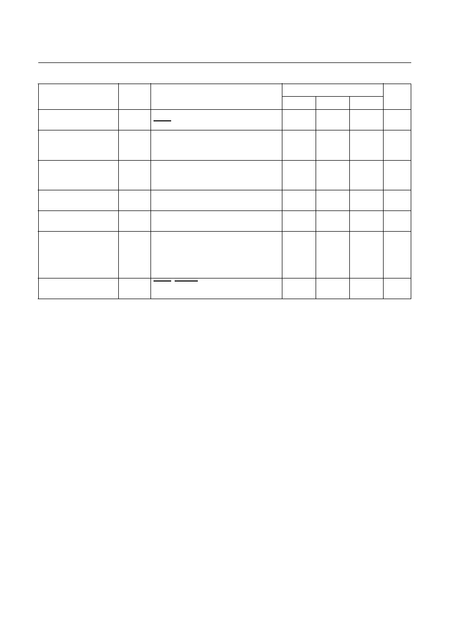
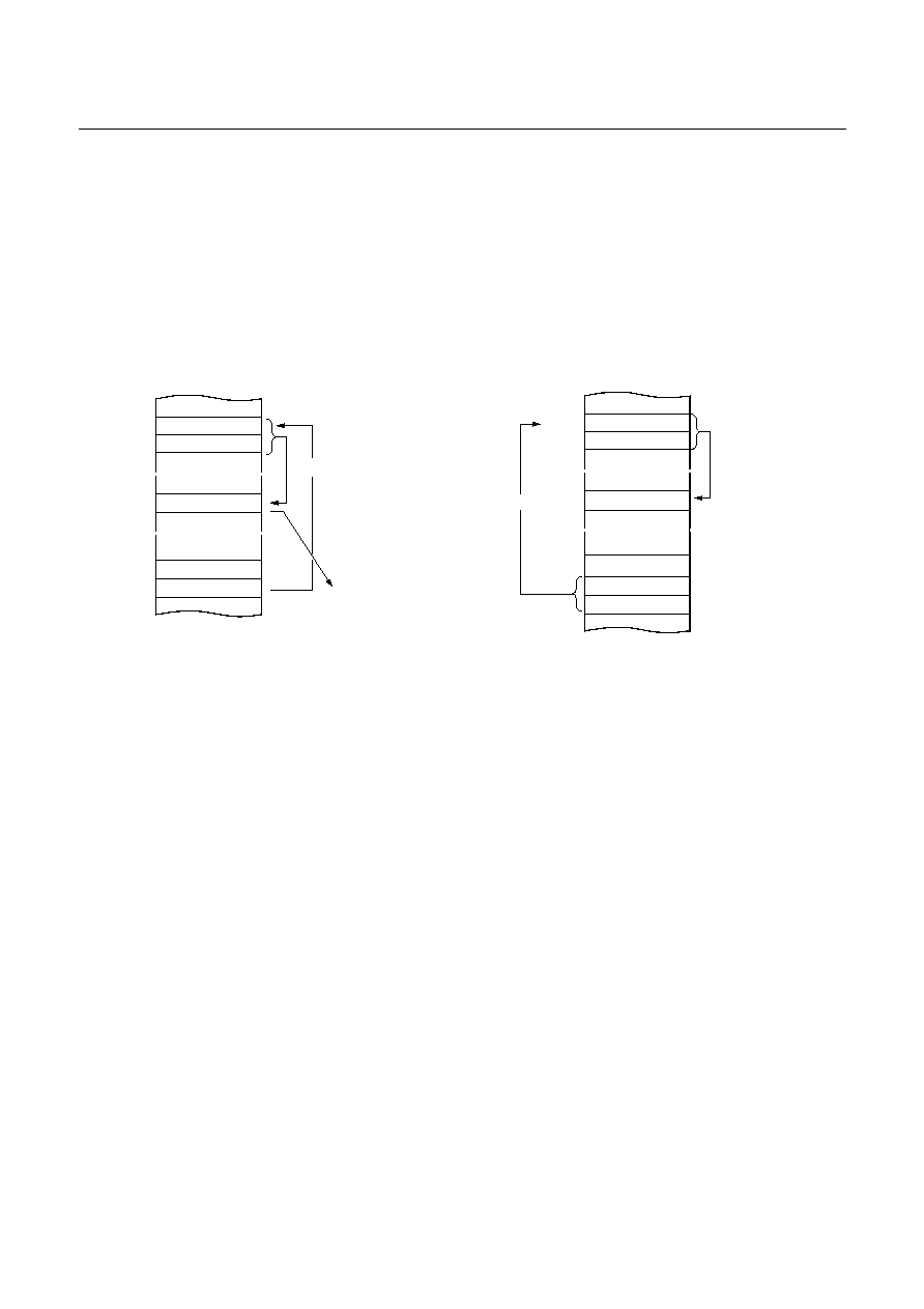
R50/BUZZ, R51/PWM8
R54/YM, R55/YS, R56/I
R, G, B
Pin
Data Reg.
Dir. Reg.
DB
DB
DB
M U X
RD
V
DD
V
SS
M U X
Buzz, PWM8
Selection
Pin
Data Reg.
DB
V
DD
V
SS
M UX
YM, YS, I
Selection
OSD ON or Data Reg Write.
Pin
R, G, B
V
DD
V
SS
i
OSD_ON

GMS81C4040/87C4060
HYUNDAI
12
May. 2000 Ver 1.0
7. ELECTRICAL CHARACTERISTICS
7.1 Absolute Maximum Ratings
Supply voltage ........................................... -0.3 to +6.0 V
Storage Temperature ................................-40 to +125
�
C
Voltage on any pin with respect to Ground (V
SS
)
............................................................... -0.3 to V
DD
+0.3
Maximum current out of V
SS
pin ........................100 mA
Maximum current into V
DD
pin ............................80 mA
Maximum current sunk by (I
OL
per I/O Pin) ........20 mA
Maximum output current sourced by (I
OH
per I/O Pin)
.................................................................................8 mA
Maximum current (
I
OL
) ...................................... 80 mA
Maximum current (
I
OH
)...................................... 50 mA
Note: Stresses above those listed under "Absolute Maxi-
mum Ratings" may cause permanent damage to the de-
vice. This is a stress rating only and functional operation of
the device at any other conditions above those indicated in
the operational sections of this specification is not implied.
Exposure to absolute maximum rating conditions for ex-
tended periods may affect device reliability.
7.2 Recommended Operating Conditions
7.3 DC Electrical Characteristics - GMS81C4040
(T
A
=-10~70
�
C, V
DD
=4.5~5.5V)
,
Parameter
Symbol
Condition
Specifications
Unit
Min.
Max.
Supply Voltage
V
DD
f
XIN
=8MHz
f
OSC
=16MHz
4.5
5.5
V
Operating Frequency
f
XIN
V
DD
=4.5~5.5V
4
8
MHz
On Screen Display Oper-
ating Frequency
f
OSC
V
DD
=4.5~5.5V
8
16
MHz
Operating Temperature
T
OPR
-10
70
�
C
Parameter
Symbol
Condition
Specifications
Unit
Min.
Typ.
Max.
High level input voltage
V
IH1
TEST, RESET, Xin, OSC1, R17~16,
R27~20, R47~44, R52, R67
0.8 V
DD
-
V
DD
V
V
IH2
R0, R15~10, R53~50
0.7 V
DD
-
V
DD
V
Low level input voltage
V
IL1
TEST, RESET, Xin, OSC1, R17~16,
R27~20, R47~44, R52, R67
0
-
0.12 V
DD
V
V
IL2
R0, R15~10, R53~50
0
-
0.3 V
DD
V
High level output voltage
V
OH
I
OH
= -5mA
R0, R1, R2, R5, R67
V
DD
- 1
-
-
V
I
OH
= -1.2mA
R,G,B
V
DD
- 1
-
-
V
Low level output voltage
V
OL
I
OL
= 5mA
R0, R1, R2, R4, R5, R67, R, G, B
-
-
1.0
V
Supply current in
ACTIVE mode
I
DD
V
DD
-
-
30
mA
HYUNDAI
GMS81C4040/87C4060
May. 2000 Ver 1.0
13
pull-up lekage current
I
RUP
V
DD
= 5.5v, V
PIN
= 0.4V
TEST
-1.5
-400
�
A
High input leakage
current
I
IZH
V
DD
= 5.5V
,
V
PIN
= V
DD
All input, I/O pins except X
IN
, OSC1,
R47~40
-5
-
5
�
A
Low input leakage
current
I
IZL
V
DD
= 5.5V
,
V
PIN
= 0V
All input, I/O pins except X
IN
, OSC1,
R47~44
-5
-
5
�
A
Open drain leakage
current
I
LOZ
V
DD
= 5.5V
,
V
OH
= V
DD
, N-ch Tr. off
R47~40
-
-
10
�
A
RAM data retention
voltage
V
RAM
V
DD
1.2
-
-
V
I
2
C port impedance
(I/O Transistor off)
R
BS
V
DD
= 4.5V
,
V
SCL0
= V
SCL1
= 2.25V
V
SDA0
= V
SDA1
= 2.25V
SCL0:SCl1 (R44:R45)
SDA0:SDA1 (R46:R47)
-
-
120
Hysterisis
Vt+ ~
Vt-
TEST, RESET, Xin, OSC1, R17~16,
R27~20, R47~44, R52, R67
1.0
-
-
V
Parameter
Symbol
Condition
Specifications
Unit
Min.
Typ.
Max.
GMS81C4040/87C4060
HYUNDAI
14
May. 2000 Ver 1.0
7.4 A/D Comparator Characteristics
(T
A
=-10~70
�
C, V
DD
=5.0V)
7.5 AC Characteristics
(T
A
=-10~70
�
C, V
DD
=5V
�
10%
,
V
SS
=0V)
Parameter
Symbol
Pins
Specifications
Unit
Min.
Typ.
Max.
Analog Input Voltage Range
V
AIN
AN0~AN5
V
SS
-
V
DD
V
Accuracy
N
FS
-
-
-
LSB
Parameter
Symbol
Pins
Specifications
Unit
Min.
Typ.
Max.
Operating Frequency
f
XIN
X
IN
4
-
8
MHz
f
OSC
OSC
8
-
16
MHz
External Clock Pulse Width
t
MCPW
X
IN
62.5
-
125
nS
t
SCPW
S
CLK
0.5
-
�
S
External Clock Transition Time
t
MRCP,
t
MFCP
X
IN
-
-
20
nS
t
SRCP,
t
SFCP
S
CLK
-
-
20
nS
Oscillation Stabilizing Time
t
ST
X
IN
, X
OUT
-
-
20
mS
Interrupt Pulse Width
t
IW
INT0~4
2
-
-
t
SYS
1
RESET Input Width
t
RST
RESET
8
-
-
t
SYS
1
Event Counter Input Pulse
Width
t
ECW
EC2, EC3
2
-
-
t
SYS
1
Event Counter Transition Time
t
REC,
t
FEC
EC2, EC3
-
-
20
nS
1. t
SYS
is one of 2/f
XIN
main clock operation mode,
HYUNDAI
GMS81C4040/87C4060
May. 2000 Ver 1.0
15
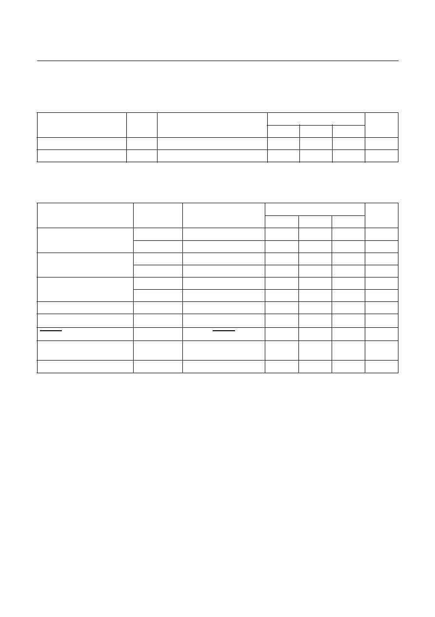
Figure 7-1 Timing Chart
t
MRCP
t
MFCP
X
IN
INT0 ~ 4
0.5V
V
DD
-0.5V
0.2V
DD
0.8V
DD
0.2V
DD
RESET
t
REC
t
FEC
0.2V
DD
0.8V
DD
EC2, EC3
t
IW
t
IW
t
RST
t
ECW
t
ECW
1/f
XIN
t
MCPW
t
MCPW
t
SRCP
t
SFCP
S
CLK
0.5V
V
DD
-0.5V
1/f
SCLK
t
SCPW
t
SCPW

GMS81C4040/87C4060
HYUNDAI
16
May. 2000 Ver 1.0
7.6 Typical Characteristics
This data will generate after evaluation.
Not available at this time.
HYUNDAI
GMS81C4040/87C4060
May. 2000 Ver 1.0
17
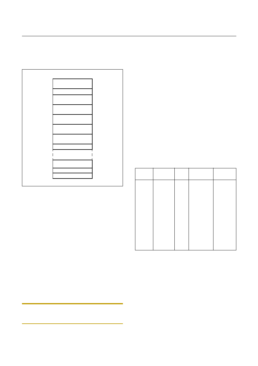
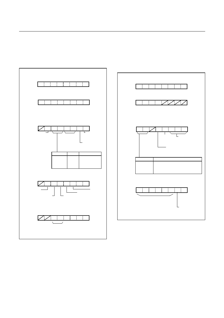
8. MEMORY ORGANIZATION
The GMS81C4040/GMS87C4060 has separate address
spaces for Program memory, Data Memory and Display
memory. Program memory can only be read, not written
to. It can be up to 40K/60K bytes of Program memory.
Data memory can be read and written to up to 1,536 bytes
including the stack area. Font memory has prepared 16K
bytes for OSD.
8.1 Registers
This device has six registers that are the Program Counter
(PC), a Accumulator (A), two index registers (X, Y), the
Stack Pointer (SP), and the Program Status Word (PSW).
The Program Counter consists of 16-bit register.
Figure 8-1 Configuration of Registers
Accumulator: The Accumulator is the 8-bit general pur-
pose register, used for data operation such as transfer, tem-
porary saving, and conditional judgement, etc.
The Accumulator can be used as a 16-bit register with Y
Register as shown below.
Figure 8-2 Configuration of YA 16-bit Register
X, Y Registers: In the addressing mode which uses these
index registers, the register contents are added to the spec-
ified address, which becomes the actual address. These
modes are extremely effective for referencing subroutine
tables and memory tables. The index registers also have in-
crement, decrement, comparison and data transfer func-
tions, and they can be used as simple accumulators.
Stack Pointer: The Stack Pointer is an 8-bit register used
for occurrence interrupts and calling out subroutines. Stack
Pointer identifies the location in the stack to be accessed
(save or restore).
Generally, SP is automatically updated when a subroutine
call is executed or an interrupt is accepted. However, if it
is used in excess of the stack area permitted by the data
memory allocating configuration, the user-processed data
may be lost.
The stack can be located at any position within 0100
H
to
01FF
H
of the internal data memory. The SP is not initial-
ized by hardware, requiring to write the initial value (the
location with which the use of the stack starts) by using the
initialization routine. Normally, the initial value of "FF
H
"
is used.
Program Counter: The Program Counter is a 16-bit wide
which consists of two 8-bit registers, PCH and PCL. This
counter indicates the address of the next instruction to be
executed. In reset state, the program counter has reset rou-
tine address (PC
H
:0FF
H
, PC
L
:0FE
H
).
Program Status Word: The Program Status Word (PSW)
contains several bits that reflect the current state of the
CPU. The PSW is described in Figure 8-3 . It contains the
Negative flag, the Overflow flag, the Break flag the Half
Carry (for BCD operation), the Interrupt enable flag, the
Zero flag, and the Carry flag.
[Carry flag C]
This flag stores any carry or borrow from the ALU of CPU
A
ACCUMULATOR
X REGISTER
Y REGISTER
STACK POINTER
PROGRAM COUNTER
PROGRAM STATUS
WORD
X
Y
SP
PCL
PCH
PSW
Two 8-bit Registers can be used as a "YA" 16-bit Register
Y
A
Y
A
Caution:
The Stack Pointer must be initialized by software be-
cause its value is undefined after RESET.
Example: To initialize the SP
LDX
#0FFH
TXSP
; SP
FF
H
SP
01
Stack Address ( 0100
H
~ 01FF
H
)
15
0
8
7
Hardware fixed
GMS81C4040/87C4060
HYUNDAI
18
May. 2000 Ver 1.0
after an arithmetic operation and is also changed by the
Shift Instruction or Rotate Instruction.
Figure 8-3 PSW (Program Status Word) Register
[Zero flag Z]
This flag is set when the result of an arithmetic operation
or data transfer is "0" and is cleared by any other result.
[Interrupt disable flag I]
This flag enables/disables all interrupts except interrupt
caused by Reset or software BRK instruction. All inter-
rupts are disabled when cleared to "0". This flag immedi-
ately becomes "0" when an interrupt is served. It is set by
the EI instruction and cleared by the DI instruction.
[Half carry flag H]
After operation, this is set when there is a carry from bit 3
of ALU or there is borrow from bit 4 of ALU. This bit can
not be set or cleared except CLRV instruction with Over-
flow flag (V).
[Break flag B]
This flag is set by software BRK instruction to distinguish
BRK from TCALL instruction with the same vector ad-
dress.
[Direct page flag G]
This flag assigns RAM page for direct addressing mode. In
the direct addressing mode, addressing area is from zero
page 00
H
to 0FF
H
when this flag is "0". If it is set to "1",
addressing area is assigned by DPGR register (address
0F8
H
). It is set by SETG instruction and cleared by CLRG.
[Overflow flag V]
This flag is set to "1" when an overflow occurs as the result
of an arithmetic operation involving signs. An overflow
occurs when the result of an addition or subtraction ex-
ceeds +127(7F
H
) or -128(80
H
). The CLRV instruction
clears the overflow flag. There is no set instruction. When
the BIT instruction is executed, bit 6 of memory is copied
to this flag.
[Negative flag N]
This flag is set to match the sign bit (bit 7) status of the re-
sult of a data or arithmetic operation. When the BIT in-
struction is executed, bit 7 of memory is copied to this flag.
N
NEGATIVE FLAG
V
G
B
H
I
Z
C
MSB
LSB
RESET VALUE : 00
H
PSW
OVERFLOW FLAG
BRK FLAG
CARRY FLAG RECEIVES
ZERO FLAG
INTERRUPT ENABLE FLAG
CARRY OUT
HALF CARRY FLAG RECEIVES
CARRY OUT FROM BIT 1 OF
ADDITION OPERLANDS
SELECT DIRECT PAGE
when G=1, page is addressed by RPR
HYUNDAI
GMS81C4040/87C4060
May. 2000 Ver 1.0
19
Figure 8-4 Stack Operation
At execution of
a CALL/TCALL/PCALL
PCL
PCH
01FF
SP after
execution
SP before
execution
01FD
01FE
01FD
01FC
01FF
Push
down
At acceptance
of interrupt
PCL
PCH
01FF
01FC
01FE
01FD
01FC
01FF
Push
down
PSW
At execution
of RET instruction
PCL
PCH
01FF
01FF
01FE
01FD
01FC
01FD
Pop
up
At execution
of RETI instruction
PCL
PCH
01FF
01FF
01FE
01FD
01FC
01FC
Pop
up
PSW
0100H
01FFH
Stack
depth
At execution
of PUSH instruction
A
01FF
01FE
01FE
01FD
01FC
01FF
Push
down
SP after
execution
SP before
execution
PUSH A (X,Y,PSW)
At execution
of POP instruction
A
01FF
01FF
01FE
01FD
01FC
01FE
Pop
up
POP A (X,Y,PSW)
GMS81C4040/87C4060
HYUNDAI
20
May. 2000 Ver 1.0
8.2 Program Memory
A 16-bit program counter is capable of addressing up to
64K bytes, but GMS81C4040/GMS87C4060 has 40K/
60K bytes program memory space only physically imple-
mented. Accessing a location above FFFF
H
will cause a
wrap-around to 0000
H
.
Figure 8-5 , shows a map of Program Memory. After reset,
the CPU begins execution from reset vector which is stored
in address FFFE
H
and FFFF
H
as shown in Figure 8-6 .
As shown in Figure 8-5 , each area is assigned a fixed lo-
cation in Program Memory. Program Memory area con-
tains the user program.
Figure 8-5 Program Memory Map
Page Call (PCALL) area contains subroutine program to
reduce program byte length by using 2 bytes PCALL in-
stead of 3 bytes CALL instruction. If it is frequently called,
it is more useful to save program byte length.
Table Call (TCALL) causes the CPU to jump to each
TCALL address, where it commences the execution of the
service routine. The Table Call service area spaces 2-byte
for every TCALL: 0FFC0
H
for TCALL15, 0FFC2
H
for
TCALL14, etc., as shown in Figure 8-7 .
Example: Usage of TCALL
The interrupt causes the CPU to jump to specific location,
where it commences the execution of the service routine.
The External interrupt 0, for example, is assigned to loca-
tion 0FFFC
H
. The interrupt service locations spaces 2-byte
interval: 0FFF8
H
and 0FFF9
H
for External Interrupt 1,
0FFFC
H
and 0FFFD
H
for External Interrupt 0, etc.
Any area from 0FF00
H
to 0FFFF
H
, if it is not going to be
used, its service location is available as general purpose
Program Memory.
Figure 8-6 Interrupt Vector Area
PROGRAM
MEMORY
TCALL
AREA
INTERRUPT
VECTOR AREA
81C4040:6000H
FEFFH
FF00H
FFC0H
FFDFH
FFE0H
FFFFH
PCALL
AREA
81C4060:1000H
FFBFH
LDA
#5
TCALL
0FH
;
1 B Y TE IN S T R U C T IO N
:
;
IN S TE A D O F 2 B Y TE S
:
;
N O R M A L C A L L
;
;TABLE CALL ROUTINE
;
FUNC_A:
LDA
LRG0
RET
;
FUNC_B:
LDA
LRG1
RET
;
;TABLE CALL ADD. AREA
;
ORG
0FFC0H
;
TC A L L A D D R E SS A R E A
DW
FUNC_A
DW
FUNC_B
1
2
0FFE0
H
E2
Address
Vector Area Memory
E4
E6
E8
EA
EC
EE
F0
F2
F4
F6
F8
FA
FC
FE
I
2
C Bus Interface Interrupt Vector Area
Serial I/O Interrupt Vector Area
Basic Interval Timer Interrupt Vector Area
Watchdog Timer Interrupt Vector Area
Timer/Counter 3 Interrupt Vector Area
Timer/Counter 1 Interrupt Vector Area
V-Sync Interrupt Vector Area
Timer/Counter 2 Interrupt Vector Area
Timer/Counter 0 Interrupt Vector Area
External Interrupt 2 Vector Area
On Screen Display Interrupt Vector Area
External Interrupt 0 Vector Area
RESET Vector Area
External Interrupt 1 Vector Area
1 Frame Timer Interrupt Vector Area
External Interrupt 3/4 Vector Area
"-" means reserved area.
NOTE:
HYUNDAI
GMS81C4040/87C4060
May. 2000 Ver 1.0
21
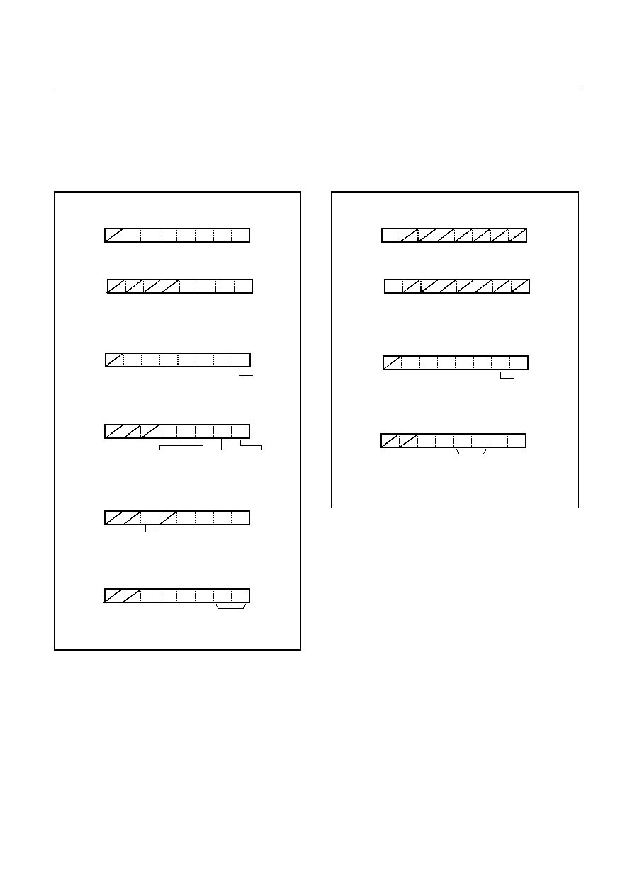
Figure 8-7 PCALL and TCALL Memory Area
PCALL
rel
4F35
PCALL
35H
TCALL
n
4A
TCALL 4
0FFC0
H
C1
Address
Program Memory
C2
C3
C4
C5
C6
C7
C8
0FF00
H
Address
PCALL Area Memory
0FFBF
H
PCALL Area
(192 Bytes)
* means that the BRK software interrupt is using
same address with TCALL0.
NOTE:
TCALL 15
TCALL 14
TCALL 13
TCALL 12
TCALL 11
TCALL 10
TCALL 9
TCALL 8
TCALL 7
TCALL 6
TCALL 5
TCALL 4
TCALL 3
TCALL 2
TCALL 1
TCALL 0 / BRK *
C9
CA
CB
CC
CD
CE
CF
D0
D1
D2
D3
D4
D5
D6
D7
D8
D9
DA
DB
DC
DD
DE
DF
4F
~
~
~
~
Sub-routine
35
0FF35H
0FF00H
0FFFFH
Upper address is
assumed 0FF
H.
11111111 11010110
01001010
PC:
F
H
F
H
D
H
6
H
4A
~
~
~
~
25
0FFD6H
0FF00H
0FFFFH
D1
Sub-routine
0FFD7H
�
�
�
0D125H
Reverse

GMS81C4040/87C4060
HYUNDAI
22
May. 2000 Ver 1.0
Example: The usage software example of Vector address and the initialize part.
ORG
0FFE0H
DW
I2C
; I2C
DW
SERIAL
; Serial I/O
DW
BIT
; Basic interval timer
DW
WATCHDOG
; Watch dog timer
DW
INT3_4
; Interrupt 3/4
DW
TIMER3
; Timer 3
DW
TIMER1
; Timer 1
DW
VSYNC
; Vertical Sync.
DW
One_Frame
; 1 Frame interrupt
DW
TIMER2
; Timer 2
DW
TIMER0
; Timer 0
DW
INT2
; Interrupt 2
DW
INT1
; Interrupt 1
DW
OSD
; On Screen Display
DW
INT0
; Interrupt 0
DW
RESET
; Reset
ORG
0F000H
;********************************************
;
MAIN PROGRAM
*
;********************************************
;
RESET:
DI
; Disable All Interrupts
LDX
#0
LDA
#0
; RAM Clear(!0000H->!00BFH)
RAM_CLR:
STA
{X}+
CMPX
#0C0H
BNE
RAM_CLR
;
CALL
LCD_CLR
; Clear LCD display memory
;
LDX
#03FH
; Stack Pointer Initialize
TXSP
LDM
R0, #0
; Normal Port 0
LDM
R0DD,#1000_0010B
; Normal Port Direction
:
:
:
:
HYUNDAI
GMS81C4040/87C4060
May. 2000 Ver 1.0
23
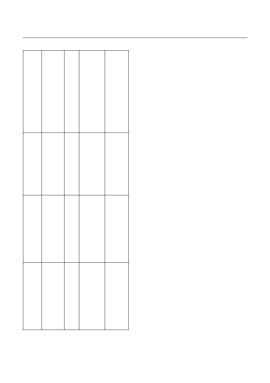
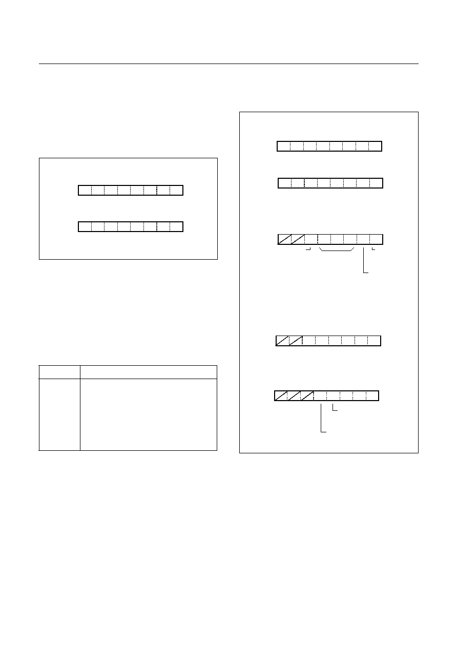
8.3 Data Memory
Figure 8-8 shows the internal Data Memory space availa-
ble. Data Memory is divided into four groups, a user RAM,
control registers, Stack, and OSD memory.
Figure 8-8 Data Memory Map
User Memory
The GMS81C4040/GMS87C4060 has 1,536
�
8 bits for
the user memory (RAM).
Control Registers
The control registers are used by the CPU and Peripheral
function blocks for controlling the desired operation of the
device. Therefore these registers contain control and status
bits for the interrupt system, the timer/ counters, analog to
digital converters and I/O ports. The basic control registers
are in address range of 00C0
H
to 00FF
H
. And OSD control
registers are assigned within 0AE0
H
~ 0AFF
H
.
Note that unoccupied addresses may not be implemented
on the chip. Read accesses to these addresses will in gen-
eral return random data, and write accesses will have an in-
determinate effect.
More detailed informations of each register are explained
in each peripheral section.
Note: Write only registers can not be accessed by bit ma-
nipulation instruction. Do not use read-modify-write instruc-
tion. Use byte manipulation instruction.
Example; To write at CKCTLR
LDM
CLCTLR,#09H ;Divide ratio
�
8
Stack Area
The stack provides the area where the return address is
saved before a jump is performed during the processing
routine at the execution of a subroutine call instruction or
the acceptance of an interrupt.
When returning from the processing routine, executing the
subroutine return instruction [RET] restores the contents of
the program counter from the stack; executing the interrupt
return instruction [RETI] restores the contents of the pro-
gram counter and flags.
The save/restore locations in the stack are determined by
the stack pointed (SP). The SP is automatically decreased
after the saving, and increased before the restoring. This
means the value of the SP indicates the stack location
number for the next save. Refer to Figure 8-4 on page 19.
Page0
RAM (192 bytes)
Peripheral Reg. (64 bytes)
0100H
00C0H
0000H
RAM (256 bytes)
0200H
RAM (256 bytes)
0300H
RAM (256 bytes)
0400H
RAM (256 bytes)
0500H
RAM (256 bytes)
0600H
RAM (64 bytes)
0A00H
OSD RAM (192 bytes)
0AE0H
Peripheral Reg. (32 bytes)
0C00H
Sprite RAM (96 bytes)
Empty area
Page1
Page2
Page3
Page4
Page5
Page6
PageA
PageC
063FH
Stack area
0C5FH
Address
Symbol
R/W
Reset Value
Addressing
mode
00C0H
00C1H
00C2H
00C3H
00C4H
00C5H
00C8H
00C9H
00CAH
00CBH
00CCH
00CDH
00CEH
00CFH
R0
R0DD
R1
R1DD
R2
R2DD
R4
R4DD
R5
R5DD
R6
R6DD
FUNC1
FUNC2
R/W
W
R/W
W
R/W
W
R/W
W
R/W
W
R/W
W
W
W
????????
00000000
????????
00000000
????????
00000000
????????
0000----
????????
----0000
?-------
0-------
-0000000
---00000
byte, bit
1
byte
2
byte, bit
byte
byte, bit
byte
byte, bit
byte
byte, bit
byte
byte, bit
byte
byte
byte
Table 8-1Control registers
GMS81C4040/87C4060
HYUNDAI
24
May. 2000 Ver 1.0
0D0H
0D1H
0D2H
0D3H
0D4H
0D5H
0D6H
0D7H
0D8H
0D9H
0DAH
0DBH
0DCH
0DEH
0DFH
TM0
TM2
TDR0
TDR1
TDR2
TDR3
BITR
CKCTLR
WDTR
ICAR
ICDR
ICSR
ICCR1
ICCR2
SIOM
SIOR
R/W
R/W
R/W
R/W
R/W
R/W
R
W
W
R/W
R/W
R/W
R/W
R/W
R/W
R/W
-0000000
-0000000
????????
????????
????????
????????
????????
--010111
-0111111
00000000
11111111
0001000-
00000000
00000000
-0000001
????????
byte
byte
byte, bit
byte, bit
byte, bit
byte, bit
byte
byte
byte
byte, bit
byte, bit
byte, bit
byte, bit
byte, bit
byte, bit
byte, bit
0E0H
0E1H
0E2H
0E3H
0E4H
0E5H
0E8H
0E9H
0EAH
0EBH
0EEH
0EFH
PWMR0
PWMR1
PWMR2
PWMR3
PWMR4
PWMR5
PWM8H
PWM8L
PWMCR1
PWMCR2
BUR
AIPS
W
W
W
W
W
W
R/W
R/W
R/W
R/W
W
W
????????
????????
????????
????????
????????
????????
????????
--??????
00000000
--0-0000
????????
--000000
byte
byte
byte
byte
byte
byte
byte, bit
byte, bit
byte, bit
byte, bit
byte
byte
0F0H
0F1H
0F2H
0F3H
0F4H
0F5H
0F6H
0F7H
0F9H
0FAH
0FBH
0FCH
0FDH
ADCM
ADR
IEDS
IMOD
IENL
IRQL
IENH
IRQH
IDCR
IDFS
IDR
DPGR
TMR
R/W
R
W
R/W
R/W
R/W
R/W
R/W
R/W
R
R
R/W
W
--011101
????????
--000000
--000000
0000000-
0000000-
00000000
00000000
0000-000
1----001
????????
----0000
????????
byte, bit
byte
byte
byte, bit
byte, bit
byte, bit
byte, bit
byte, bit
byte, bit
byte
byte
byte, bit
byte
0AE0H
0AE1H
0AE2H
0AE3H
0AE4H
0AE5H
0AE6H
0AE8H
0AE9H
0AF0H
0AF1H
0AF3H
0AF4H
OSDcon1
OSDcon2
OSDPOL
FDWSET
EDGEcol
OSDLN
LHPOS
SPVPOS
SPHPOS
L1ATTR
L1VPOS
L2ATTR
L2VPOS
R/W
R/W
W
W
W
R
W
W
W
W
W
W
W
00000000
-0000000
????????
01111010
10000111
---00000
????????
????????
????????
????????
????????
????????
????????
byte, bit
byte, bit
byte
byte
byte
byte
byte
byte
byte
byte
byte
byte
byte
Table 8-1Control registers
1. "byte, bit" means that register can be addressed by not only bit
but byte manipulation instruction.
2. "byte" means that register can be addressed by only byte
manipulation instruction. On the other hand, do not use any
read-modify-write instruction such as bit manipulation for clear-
ing bit.
HYUNDAI
GMS81C4040/87C4060
May. 2000 Ver 1.0
25
8.4 Addressing Mode
The GMS800 series uses six addressing modes;
� Register addressing
� Immediate addressing
� Direct page addressing
� Absolute addressing
� Indexed addressing
� Register-indirect addressing
(1) Register Addressing
Register addressing accesses the A, X, Y, C and PSW.
(2) Immediate Addressing
#imm
In this mode, second byte (operand) is accessed as a data
immediately.
Example:
FE10: 0435
ADC
#35H
When G-flag is 1, then RAM address is defined by 16-bit
address which is composed of 8-bit direct page accessable
register (DPGR) and 8-bit immediate data.
Example: G=1, DPGR=0CH
F100: E45535
LDM
35H,#55H
(3) Direct Page Addressing
dp
In this mode, a address is specified within direct page.
Example; G=0
E551: C535
LDA
35H;A
RAM[35H]
(4) Absolute Addressing
!abs
Absolute addressing sets corresponding memory data to
Data , i.e. second byte(Operand I) of command becomes
lower level address and third byte (Operand II) becomes
upper level address.
With 3 bytes command, it is possible to access to whole
memory area.
ADC, AND, CMP, CMPX, CMPY, EOR, LDA, LDX,
LDY, OR, SBC, STA, STX, STY
Example;
F100: 0735F0 ADC!0F035H
;A
ROM[0F035H]
35
A+35H+C
A
04
MEMORY
0FE10
H
E4
0F100
H
data
55H
~
~
~
~
data
0C35
H
�
35
0F102
H
55
0F101
H
A
data
35
35
H
0E551
H
data
A
�
�
~
~
~
~
C5
0E550
H
07
0F100
H
~
~
~
~
data
0F035
H
P
F0
0F102
H
35
0F101
H
A
A+data+C
A
address: 0F035
GMS81C4040/87C4060
HYUNDAI
26
May. 2000 Ver 1.0
The operation within data memory (RAM)
ASL, BIT, DEC, INC, LSR, ROL, ROR
Example; Addressing accesses the address 0135
H
regard-
less of G-flag and DPGR.
F100: 983501 INC!0135H
;A
ROM[135H]
(5) Indexed Addressing
X indexed direct page (no offset)
{X}
In this mode, a address is specified by the X register.
ADC, AND, CMP, EOR, LDA, OR, SBC, STA, XMA
Example; X=15
H
, G=1, DPGR=03
H
E550: D4
LDA
{X};ACC
RAM[X].
X indexed direct page, auto increment
{X}+
In this mode, a address is specified within direct page by
the X register and the content of X is increased by 1.
LDA, STA
Example; G=0, X=35
H
F100: DB
LDA
{X}+
X indexed direct page (8 bit offset)
dp+X
This address value is the second byte (Operand) of com-
mand plus the data of
-register. And it assigns the mem-
ory in Direct page.
ADC, AND, CMP, EOR, LDA, LDY, OR, SBC, STA
STY, XMA, ASL, DEC, INC, LSR, ROL, ROR
Example; G=0, X=0F5
H
E550: C645
LDA
45H+X
98
0F100
H
~
~
~
~
data
135
H
�
01
0F102
H
35
0F101
H
�
data+1
data
�
address: 0135
data
D4
315
H
0E550
H
data
A
�
�
~
~
~
~
data
DB
35
H
data
A
�
�
~
~
~
~
36H
X
0F100
H
data
45
3A
H
0E551
H
data
A
�
�
~
~
~
~
C6
0E550
H
45H+0F5H=13AH
�
HYUNDAI
GMS81C4040/87C4060
May. 2000 Ver 1.0
27
Y indexed direct page (8 bit offset)
dp+Y
This address value is the second byte (Operand) of com-
mand plus the data of Y-register, which assigns Memory in
Direct page.
This is same with above (2). Use Y register instead of X.
Y indexed absolute
!abs+Y
Sets the value of 16-bit absolute address plus Y-register
data as Memory. This addressing mode can specify mem-
ory in whole area.
Example; Y=55
H
F100: D500FA
LDA
!0FA00H+Y
(6) Indirect Addressing
Direct page indirect
[dp]
Assigns data address to use for accomplishing command
which sets memory data(or pair memory) by Operand.
Also index can be used with Index register X,Y.
JMP, CALL
Example; G=0
FA00: 3F35
JMP
[35H]
X indexed indirect
[dp+X]
Processes memory data as Data, assigned by 16-bit pair
m e m o r y w h i c h i s d e t e r m i n e d b y p a i r d a t a
[dp+X+1][dp+X] Operand plus X-register data in Direct
page.
ADC, AND, CMP, EOR, LDA, OR, SBC, STA
Example; G=0, X=10
H
FA00: 1625
ADC
[25H+X]
D5
0F100
H
data
A
�
~
~
~
~
data
0FA55
H
0FA00H+55H=0FA55H
�
FA
0F102
H
00
0F101
H
�
0A
35
H
jump to address 0E30A
H
�
~
~
~
~
35
0FA00
H
E3
36
H
�
3F
0E30A
H
NEXT
~
~
~
~
05
35
H
0E005
H
~
~
~
~
25
0FA00
H
E0
36
H
16
0E005
H
data
~
~
~
~
�
A + data + C
A
25 + X(10) = 35
H
�
�
GMS81C4040/87C4060
HYUNDAI
28
May. 2000 Ver 1.0
Y indexed indirect
[dp]+Y
Processes momory data as Data, assigned by the data
[dp+1][dp] of 16-bit pair memory paired by Operand in Di-
rect page plus Y-register data.
ADC, AND, CMP, EOR, LDA, OR, SBC, STA
Example; G=0, Y=10
H
FA00: 1725
ADC
[25H]+Y
Absolute indirect
[!abs]
The program jumps to address specified by 16-bit absolute
address.
JMP
Example; G=0
FA00: 1F25E0
JMP
[!0C025H]
05
25
H
0E005
H
+ Y(10) = 0E015
H
�
~
~
~
~
25
0FA00
H
E0
26
H
�
17
0E015
H
data
~
~
~
~
�
A + data + C
A
25
0E025
H
jump to
~
~
~
~
E0
0FA00
H
E7
0E026
H
�
25
0E725
H
NEXT
~
~
~
~
1F
PROGRAM MEMORY
�
address 0E30A
H
HYUNDAI
GMS81C4040/87C4060
May. 2000 Ver 1.0
29
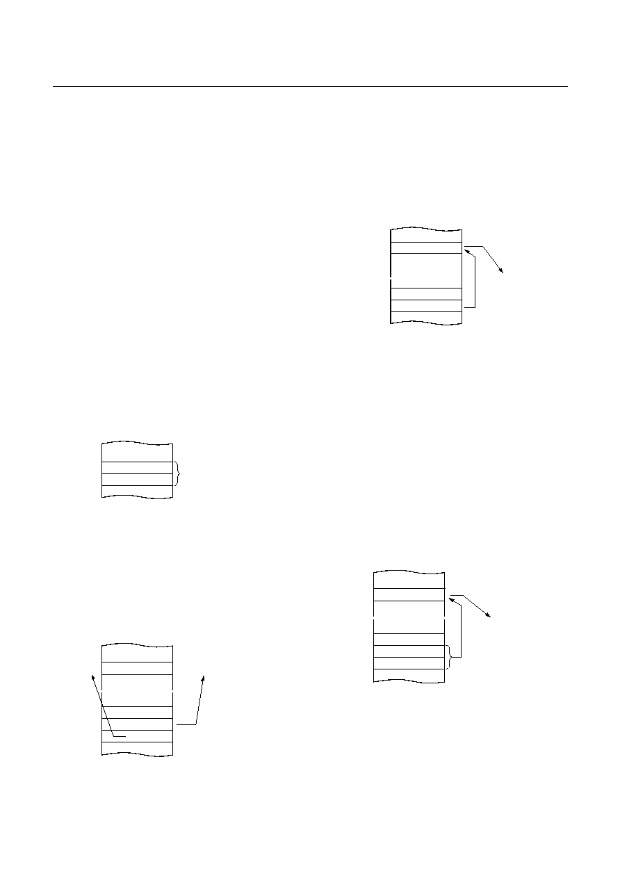
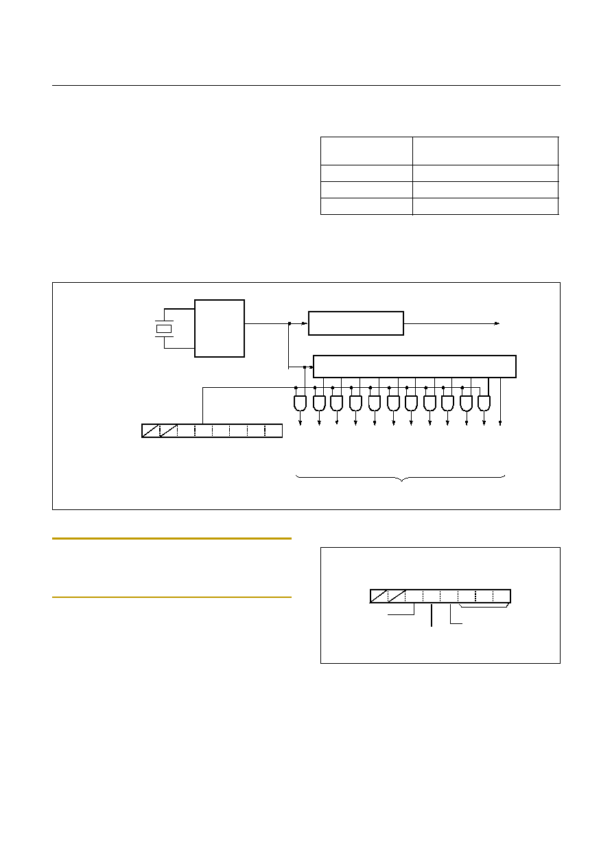
9. I/O PORTS
The GMS81C4040/GMS87C4060 has digital ports (R0,
R1, R2, R4, R5 and R6) and OSD ports (R,G,B).
These ports pins may be multiplexed with an alternate
function for the peripheral features on the device. In gen-
eral, in a initial reset state, R ports are used as a general
purpose digital port.
9.1 Registers for Port
Port Data Registers
The Port Data Registers in I/O buffer in each R ports are
represented as a Type D flip-flop, which will clock in a val-
ue from the internal bus in response to a "write to data reg-
ister" signal from the CPU. The Q output of the flip-flop is
placed on the internal bus in response to a "read data reg-
ister" signal from the CPU. The level of the port pin itself
is placed on the internal bus in response to "read data reg-
ister" signal from the CPU. Some instructions that read a
port activating the "read register" signal, and others acti-
vating the "read pin" signal
Port Direction Registers
All pins have data direction registers which can define
these ports as output or input. A "1" in the port direction
register configure the corresponding port pin as output.
Conversely, write "0" to the corresponding bit to specify it
as input pin. For example, to use the even numbered bit of
R0 as output ports and the odd numbered bits as input
ports, write "55
H
" to address 0C1
H
(R0 port direction reg-
ister) during initial setting as shown in Figure 9-1 .
All the port direction registers in the GMS81C4040/
GMS87C4060 have 0 written to them by reset function. On
the other hand, its initial status is input.
Figure 9-1 Example of port I/O assignment
I : INPUT PORT
WRITE "55
H
" TO PORT R0 DIRECTION REGISTER
0
1
0
1
0
1
0
1
I
O
I
O
I
O
I
O
R0 DATA
R4 DATA
R0 DIRECTION
R4 DIRECTION
0C0H
0C1H
0C8H
0C9H
7
6
5
4
3
2
1
0
BIT
7
6
5
4
3
2
1
0
PORT
O : OUTPUT PORT
~
~
~
~
GMS81C4040/87C4060
HYUNDAI
30
May. 2000 Ver 1.0
9.2 I/O Ports Configuration
R0 Ports
R0 is an 8-bit CMOS bidirectional I/O port (address
0C0
H
). Each I/O pin can independently used as an input or
an output through the R0DD register (address 0C1
H
).
The control registers for R0 are shown below.
In addition, Port R0 is only digital I/O. After reset, R0DD
value is "0", R0 acts as normal digital input port.
R1 Ports
R1 is an 8-bit CMOS bidirectional I/O port (address
0C2
H
). Each I/O pin can independently used as an input or
an output through the R1DD register (address 0C3
H
).
R1 port have secondary functions as following table.
The control registers for R1 are shown below.
Port R1 is multiplexed with various special features.The
control registers controls the selection of alternate func-
tion. After reset, R1 port acts as normal digital input port.
The way to select alternate function such as A/D input or
HD,VD will be shown in each peripheral section.
Port Pin
Alternate Function
R10
R11
R12
R13
R14
R15
R16
R17
AN0 (A/D input 0)
AN1 (A/D input 1)
AN2 (A/D input 2)
AN3 (A/D input 3)
AN4 (A/D input 4)
AN5 (A/D input 5)
VD (Vertical Sync. input)
HD (Horizontal Sync. input)
R0 Data Register
R0
ADDRESS : 00C0
H
RESET VALUE : Undefined
R07
R06
R05
R04
R03
R02
R01
R00
Port Direction
R0 Direction Register
R0DD
ADDRESS : 00C1
H
RESET VALUE : 0000 0000
b
0: Input
1: Output
RW
RW
RW
RW
RW
RW
RW
RW
W
W
W
W
W
W
W
W
R1 Data Register
R1
ADDRESS : 00C2
H
RESET VALUE : Undefined
R17
R16
R15
R14
R13
R12
R11
R10
Port Direction
R1 Direction Register
R1DD
ADDRESS : 00C3
H
RESET VALUE : 0000 0000
b
0: Input
1: Output
A/D Convertor mode Register
ADCM
ADDRESS : 00F0
H
RESET VALUE : --01 1101
b
Port Property
Analog input pin selector Register
AIPS
ADDRESS : 00EF
H
RESET VALUE : --00 0000
b
0: Digital I/O
1: Analog Input
R16/VD select
Port function select Register 2
FUNC2
ADDRESS : 00CF
H
RESET VALUE : ---0 0000
b
0: R16 I/O
1: VD Input
ADEN ADS2 ADS1 ADS0 ADST ADSF
HDS
VDS
YMS
YSS
IS
A/D Status
0: Busy
1: Finish
A/D Start
0: Ignore
1: A/D start
A/D Port select
000: AN0
001: AN1
A/D Enable
0: Disable
1: Enable
010: AN2
011: AN3
100: AN4
101: AN5
110: AN6
111: No Analog port
R17/HD select
0: R17 I/O
1: HD Input
RW
RW
RW
RW
RW
RW
RW
RW
RW
RW
RW
RW
RW
R
W
W
W
W
W
W
W
W
W
W
W
W
W
W
W
W
W
W
W
HYUNDAI
GMS81C4040/87C4060
May. 2000 Ver 1.0
31
R2 Port
R2 is an 8-bit CMOS bidirectional I/O port (address
0C4
H
). Each I/O pin can independently used as an input or
an output through the R2DD register (address 00C5
H
).
The control registers for R2 are shown below.
R4 Port
R4 is consrutced with 4-bit Open drain Output port and 4-
bit CMOS bidirectional I/O port (address 0C8
H
). Each I/O
pin can independently used as an input or an output
through the R4DD register (address 0C9
H
).
The control registers for R4 are shown below.
R2 Data Register
R2
ADDRESS : 00C4
H
RESET VALUE : Undefined
R27
R26
R25
R24
R23
R22
R21
R20
Port Direction
R2 Direction Register
R2DD
ADDRESS : 00C5
H
RESET VALUE : 0000 0000
b
0: Input
1: Output
Serial I/O mode Register
SIOM
ADDRESS : 00DE
H
RESET VALUE : -000 0001
b
00: Ignore edge
Ext. interrupt edge selection Register
IEDS
ADDRESS : 00F2
H
RESET VALUE : --00 0000
b
01: Falling edge
10: Rising edge
R20/INT2
Port function select Register 1
FUNC1
ADDRESS : 00CE
H
RESET VALUE : -000 0000
b
0: R20
1: INT2
SM1
SM0
SCK1 SCK0 SIOST SIOSF
INT4S INT3S INT2S INT1S INT0S
Seriial Status
0: Busy
1: Finish
Serial Start
0: Ignore
1: Serial start
Clock select
00: PS3
01: PS4
Serial I/O
0: Serial In
1: Serial Out
10: PS5
11: External
IOSW
EC2S
EC3S
SM1
0
0
1
1
SM0
0
1
0
1
Mode
-
Send
Receive
-
R21
R21
Sclk
Sclk
R21
R22
R22
Sout
R22
R22
R23
R23
R23
Sin
R23
R24/INT3
0: R24
1: INT3
R26/INT4
0: R26
1: INT4
R27/EC3
0: R27
1: EC3
R25/EC2
0: R25
1: EC2
IED2H IED2L
IED1H IED1L IED0H IED0L
11: Falling/Rising edge
INT2
RW
RW
RW
RW
RW
RW
RW
RW
W
W
W
W
W
W
W
W
RW
RW
RW
RW
RW
RW
R
W
W
W
W
W
W
W
W
W
W
W
W
W
R4 Data Register
R4
ADDRESS : 00C8
H
RESET VALUE : Undefined
R47
R46
R45
R44
R43
R42
R41
R40
Port Direction
R4 Direction Register
R4DD
ADDRESS : 00C9
H
RESET VALUE : 0000 ----
b
0: Input
1: Output
I
2
C Control Register 1
ICCR1
ADDRESS : 00DB
H
RESET VALUE : 00-0 0000
b
EN5,4,3,2,1 : R47,45,43,42,41,40
PWM control Register 1
PWMCR1
ADDRESS : 00EA
H
RESET VALUE : 0000 0000
b
0: R4x acts normal digital port
1: R4x acts PWM output port
ALS
ESO
BC2
BC1
BC0
EN2
EN1
EN0
EN8
CNT
Bit count
000
b
(8bit)
I
2
C enable
0: Disable
1: Enable
BSW0
EN3
EN4
EN5
BSW1
0
0
1
1
BSW0
0
1
0
1
R44
R44
SCL0
R44
SCL
R45
R45/PWM4
R45/PWM4
SCL1
SCL
R46
R46
SDA0
R46
SDA
BSW1
001
b
~111
b
(1~7bit)
R47
R47/PWM5
R47/PWM5
SDA1
SDA
Slave address identification
0: Accept (Addressing format)
1: Decline (Free data format)
RW
RW
RW
RW
RW
RW
RW
RW
W
W
W
W
W
W
W
W
RW
RW
RW
RW
RW
RW
RW
RW
RW
RW
RW
RW
RW
RW
RW
14/8bit PWM count
0: Count start
1: Count stop
R51/PWM8 select
0: R51
1: PWM8
GMS81C4040/87C4060
HYUNDAI
32
May. 2000 Ver 1.0
R5 Port
R5 is an 7-bit port (address 0CA
H
). Each I/O pin can inde-
pendently used as an input or an output through the R5DD
register (address 0CB
H
).
The control registers for R5 are shown below
R6 Port
R6 is an 1-bit CMOS bidirectional I/O port (address
0CC
H
). Each I/O pin can independently used as an input or
an output through the R6DD register (address 0CD
H
).
The control registers for R6 are shown below
R5 Data Register
R5
ADDRESS : 00CA
H
RESET VALUE : Undefined
R56
R55
R54
R53
R52
R51
R50
Port Direction
R5 Direction Register
R5DD
ADDRESS : 00CB
H
RESET VALUE : ---- 0000
b
0: Input
1: Output
00: Ignore edge
Ext. interrupt edge selection Register
IEDS
ADDRESS : 00F2
H
RESET VALUE : --00 0000
b
01: Falling edge
10: Rising edge
R52/INT0
Port function select Register 1
FUNC1
ADDRESS : 00CE
H
RESET VALUE : -000 0000
b
0: R52
1: INT0
INT4S INT3S INT2S INT1S INT0S
EC2S
EC3S
IED2H IED2L
IED1H IED1L IED0H IED0L
11: Falling/Rising edge
R56/I
Port function select Register 2
FUNC2
ADDRESS : 00CF
H
RESET VALUE : ---0 0000
b
0: R56
1: I Output
HDS
VDS
YMS
YSS
IS
R55/YS
0: R55
1: YS Output
R54/YM
0: R56
1: YM Output
PWM control Register 2
PWMCR2
ADDRESS : 00EB
H
RESET VALUE : --0- 0000
b
POL2 POL1
EN7
EN6
BUZS
INT2
R50/BUZZ
0: R50
1: BUZZ
RW
RW
RW
RW
RW
RW
RW
W
W
W
W
W
W
W
W
W
W
W
W
W
W
W
W
RW
RW
RW
RW
RW
W
W
W
W
W
W
R6 Data Register
R6
ADDRESS : 00CC
H
RESET VALUE : Undefined
Port Direction
R6 Direction Register
R6DD
ADDRESS : 00CD
H
RESET VALUE : 0--- ----
b
0: Input
1: Output
00: Ignore edge
Ext. interrupt edge selection Register
IEDS
ADDRESS : 00F2
H
RESET VALUE : --00 0000
b
01: Falling edge
10: Rising edge
R67/INT1
Port function select Register 1
FUNC1
ADDRESS : 00CE
H
RESET VALUE : -000 0000
b
0: R67
1: INT1
INT4S INT3S INT2S INT1S INT0S
EC2S
EC3S
IED2H IED2L
IED1H IED1L IED0H IED0L
11: Falling/Rising edge
INT1
RW
W
W
W
W
W
W
W
W
W
W
W
W
W
R67
W
HYUNDAI
GMS81C4040/87C4060
May. 2000 Ver 1.0
33
10. CLOCK GENERATOR
As shown in Figure 10-1 , the clock generator produces the
basic clock pulses which provide the system clock to be
supplied to the CPU and the peripheral hardware. It con-
tains two oscillators: a main-frequency clock oscillator and
a sub-frequency clock oscillator. The system clock can
also be obtained from the external oscillator.
The clock generator produces the system clocks forming
clock pulse, which are supplied to the CPU and the periph-
eral hardware.
To the peripheral block, the clock among the not-divided
original clocks, divided by
2
, 4,...,
up to 1024 can be pro-
vided. Peripheral clock is enabled or disabled by bit 4 of
the peripheral clock enable register (ENPCK).
Figure 10-1 Block Diagram of Clock Generator
Note: On the initial reset, all peripherals are run because
peripheral clock is supplied to each function block. If you
want to see more details, see Clock Control Register
(CKCTLR).
Main clock
Minimum instruction cycle time
(ex:NOP ; f
ex
4clock is needed)
3.6MHz
1,111nS
4MHz
1,000nS
8MHz
500nS
Internal system clock
P R E SC A LE R
ENPCK
�
1
Peripheral clock
f
EX
Clock control register
[0D6
H
]
CKCTLR
WDT ENPCK BTCL BTS2 BTS1 BTS0
Clock pulse Generator
ON
OSC
Circuit
PS0
PS1
PS2
PS3
PS4
PS5
PS6
PS7
PS8
PS9
PS1
0
PS1
1
�
2
�
4
�
8
�
16
�
32
�
64
�
12
8
�
25
6
�
51
2
�
10
24
�
20
48
Clock control register
ADDRESS : 00D6
H
RESET VALUE : --01 0111
b
CKCTLR
WDT ENPCK BTCL BTS2 BTS1 BTS0
ON
Peri. Clock
0: Stop
1: Supply
Watch-dog
timer select
0: Normal 6bit timer
1: Watch-dog timer
B.I.T set
0: Free run
1: B.I.T clear
B.I.T Clock
W
W
W
W
W
W
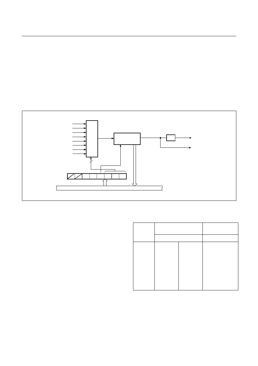
GMS81C4040/87C4060
HYUNDAI
34
May. 2000 Ver 1.0
11. TIMER
11.1 Basic Interval Timer
The GMS81C4040/GMS87C4060 has one 8-bit Basic In-
terval Timer that is free-run and can not be stopped. Block
diagram is shown in Figure 11-1 .
The Basic Interval Timer generates the time base for
watchdog timer counting, and etc. It also provides a Basic
interval timer interrupt (BITIF). As the count overflow
from FF
H
to 00
H
, this overflow causes the interrupt to be
generated. The Basic Interval Timer is controlled by the
clock control register (CKCTLR) shown in Figure 11-2 .
Source clock can be selected by lower 3 bits of CKCTLR.
BITR and CKCTLR are located at same address, and ad-
dress 00D6
H
is read as a BITR and written to CKCTLR..
Figure 11-1 Block Diagram of Basic Interval Timer
Table 11-1 Basic Interval Timer Interrupt Time
MUX
Basic Interval Timer Interrupt
BITR
Select Input clock
3
source
clock
8-bit up-counter
BITCK
BTCL
f
ex
�
2
10
f
ex
�
2
9
f
ex
�
2
8
f
ex
�
2
7
f
ex
�
2
6
f
ex
�
2
5
f
ex
�
2
4
Watchdog timer clock (WDTCK)
clear
overflow
Internal bus line
[0D6
H
]
[0D6
H
]
BITIF
Clock control register
CKCTLR
WDT ENPCK BTCL BTS2 BTS1 BTS0
ON
PS4
PS5
PS6
PS7
PS8
PS9
PS10
PS11
f
ex
�
2
11
BTS2~0
Source clock
Interrupt
(overflow) Period
P re -S cale r o utpu t
At f
ex
=8MHz
000
001
010
011
100
101
110
111
PS4
PS5
PS6
PS7
PS8
PS9
PS10
PS11
f
ex
�
2
4
f
ex
�
2
5
f
ex
�
2
6
f
ex
�
2
7
f
ex
�
2
8
f
ex
�
2
9
f
ex
�
2
10
f
ex
�
2
11
0.512
1.024
2.048
4.096
8.192
16.384
32.768
65.536
mS
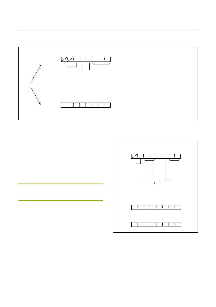
HYUNDAI
GMS81C4040/87C4060
May. 2000 Ver 1.0
35
Figure 11-2 BITR: Basic Interval Timer Mode Register
11.2 Timer 0, 1
Timer 0, 1 consists of prescaler, multiplexer, 8-bit compare
data register, 8-bit count register, Control register, and
Comparator as shown in Figure 11-3 .
These Timers can run separated 8bit timer or combined
16bit timer. These timers are operated by internal clock.
The contents of TDR1 are compared with the contents of
up-counter T1. If a match is found, a timer/counter 1 inter-
rupt (T1IF) is generated, and the counter is cleared. Count-
ing up is resumed after the counter is cleared.
Note: You can read Timer 0, Timer 1 value from TDR0 or
TDR1. But if you write data to TDR0 or TDR1, it changes
Timer 0 or Timer 1 modulo data, not Timer value.
The content of TDR0, TDR1 must be initialized (by soft-
ware) with the value between 01
H
and FF
H
,not to 00
H
.
Or not, Timer 0 or Timer 1 can not count up forever.
The control registers for Timer 0,1 are shown below.
CKCTLR
INITIAL VALUE: Undefined
ADDRESS: 00D6
H
BITR
Both register are in same address,
when write, to be a CKCTLR,
when read, to be a BITR.
Caution:
8-BIT BINARY COUNTER
ADDRESS : 00D6
H
RESET VALUE : --01 0111
b
WDT ENPCK BTCL BTS2 BTS1 BTS0
ON
Peri. Clock
0: Stop
1: Supply
Watch-dog
timer select
0: Normal 6bit timer
1: Watch-dog timer
B.I.T set
0: Free run
1: Clear 8-bit counter (BITR) to "0". This bit becomes 0
B.I.T Clock
automatically after 1 machine cycle
W
W
W
W
W
W
R
R
R
R
R
R
R
R
Timer mode register 0
TM0
ADDRESS : 00D0
H
RESET VALUE : -000 0000
b
Timer 0 data register
TDR0
ADDRESS : 00D2
H
RESET VALUE : Undefined
T1SL0 T0ST
T0CN T0SL1 T0SL0
T1SL1
T1ST
Timer 1 data register
TDR1
ADDRESS : 00D3
H
RESET VALUE : Undefined
Timer 0 input clock
00: PS2 (f
ex
/ 2
2
)
01: PS4 (f
ex
/ 2
4
)
10: PS6 (f
ex
/ 2
6
)
11: PS8 (f
ex
/ 2
8
)
Timer 1 input clock
00: Timer 0 overflow (16bit mode)
01: PS2 (f
ex
/ 2
2
)
10: PS4 (f
ex
/ 2
4
)
11: PS6 (f
ex
/ 2
6
)
0: Count Hold
1: Count Continue
Timer 0 control
0: Count Hold
1: Count Clear and Start
Timer 0 start
0: Count Hold
1: Count Clear and Start
Timer 1 start
RW
RW
RW
RW
RW
RW
RW
RW
RW
RW
RW
RW
RW
RW
RW
RW
RW
RW
RW
RW
RW
RW
RW
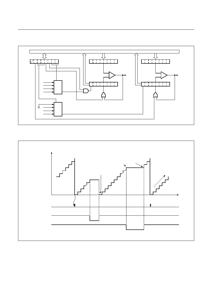
GMS81C4040/87C4060
HYUNDAI
36
May. 2000 Ver 1.0
.
Figure 11-3 Simplified Block Diagram of 8bit Timer0, 1
Figure 11-4 Count Example of Timer
8bit Comparator
Internal bus line
TM0
TDR0
Timer 0
T0IF
Clock
TDR1
Timer 1
Clock
Clear
Clear
8bit Comparator
T1IF
MUX
PS2
PS4
PS6
PS8
MUX
NC
PS2
PS4
PS6
T0CN
T0ST
T1ST
Timer 0 (T0IF)
Interrupt
TDR0
TIME
Occur interrupt
Occur interrupt
stop
clear & start
disable
enable
Start & Stop
T0ST
T0CN
Control count
up-
co
unt
~~
~~
T0ST = 0
T0ST = 1
T0CN = 0
T0CN = 1
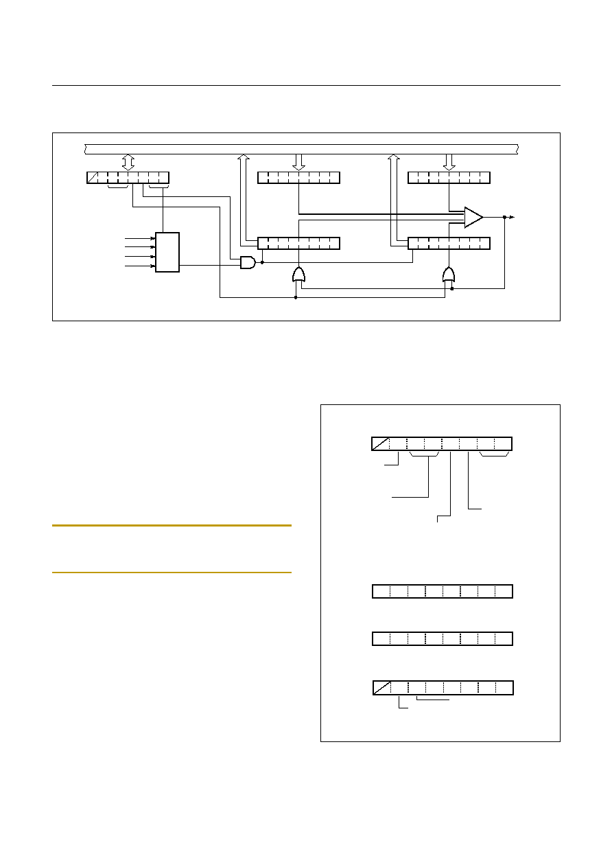
HYUNDAI
GMS81C4040/87C4060
May. 2000 Ver 1.0
37
Figure 11-5 Simplified Block Diagram of 16bit Timer0, 1
11.3 Timer / Event Counter 2, 3
Timer 2, 3 consists of prescaler, multiplexer, 8-bit compare
data register, 8-bit count register, Control register, and
Comparator as shown in Figure 11-5 .
These Timers have two operating modes. One is the timer
mode which is operated by internal clock, other is event
counter mode which is operated by external clock from pin
R25/EC2, R27/EC3.
These Timers can run separated 8bit timer or combined
16bit timer.
Note: You can read Timer 2, Timer 3 value from TDR2 or
TDR3. But if you write data to TDR2 or TDR3, it changes
Timer 2 or Timer 3 modulo data, not Timer value.
The content of TDR2, TDR3 must be initialized (by soft-
ware) with the value between 01
H
and FF
H
,not to 00
H
.
Or not, Timer 2 or Timer 3 can not count up forever.
The control registers for Timer 2,3 are shown below
Internal bus line
TM0
TDR0
Timer 0
Clock
TDR1
Timer 1
Clock
Clear
Clear
16bit Comparator
T1IF
MUX
PS2
PS4
PS6
PS8
T0CN
T0ST
0
0
Timer mode register 2
TM2
ADDRESS : 00D1
H
RESET VALUE : -000 0000
b
Timer 2 data register
TDR2
ADDRESS : 00D4
H
RESET VALUE : Undefined
T3SL0 T2ST
T2CN T2SL1 T2SL0
T3SL1
T3ST
Timer 3 data register
TDR3
ADDRESS : 00D5
H
RESET VALUE : Undefined
Timer 2 input clock
00: PS2 (f
ex
/ 2
2
)
01: PS4 (f
ex
/ 2
4
)
10: PS6 (f
ex
/ 2
6
)
11: PS8 (f
ex
/ 2
8
)
Timer 3 input clock
00: Timer 2 overflow (16bit mode)
01: PS2 (f
ex
/ 2
2
)
10: PS4 (f
ex
/ 2
4
)
11: PS6 (f
ex
/ 2
6
)
0: Count Hold
1: Count Continue
Timer 2 control
0: Count Hold
1: Count Clear and Start
Timer 2 start
0: Count Hold
1: Count Clear and Start
Timer 3 start
Port function select Register 1
FUNC1
ADDRESS : 00CE
H
RESET VALUE : -000 0000
b
INT4S INT3S INT2S INT1S INT0S
EC2S
EC3S
R27/EC3
0: R27
1: EC3
R25/EC2
0: R25
1: EC2
RW
RW
RW
RW
RW
RW
RW
RW
RW
RW
RW
RW
RW
RW
RW
RW
RW
RW
RW
RW
RW
RW
RW
W
W
W
W
W
W
W

GMS81C4040/87C4060
HYUNDAI
38
May. 2000 Ver 1.0
.
Figure 11-6 Simplified Block Diagram of 8bit Timer/Event Counter 2,3
Figure 11-7 Count Example of Timer / Event counter
8bit Comparator
Internal bus line
TM2
TDR2
Timer 2
T2IF
Clock
TDR3
Timer 3
Clock
Clear
Clear
8bit Comparator
T3IF
MUX
EC2
PS2
PS4
PS6
MUX
NC
EC3
PS2
PS4
T2CN
T2ST
T3ST
Timer 2 (T2IF)
Interrupt
TDR2
TIME
Occur interrupt
Occur interrupt
stop
clear & start
disable
enable
Start & Stop
T2ST
T2CN
Control count
up-
co
unt
~~
~~
T2ST = 0
T2ST = 1
T2CN = 0
T2CN = 1
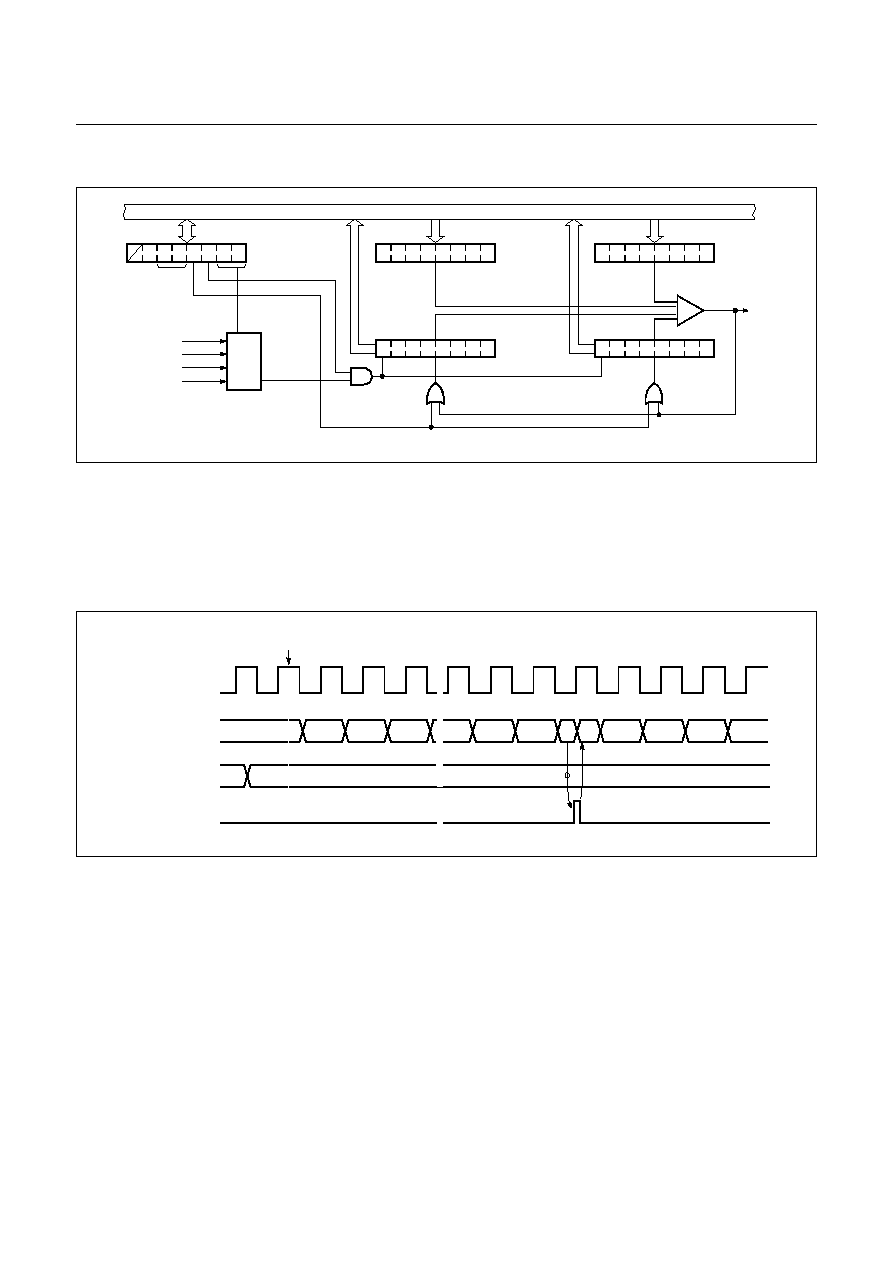
HYUNDAI
GMS81C4040/87C4060
May. 2000 Ver 1.0
39
Figure 11-8 Simplified Block Diagram of 16bit Timer/Event Counter 2,3
Timer Mode
In the timer mode, the internal clock is used for counting
up. Thus, you can think of it as counting internal clock in-
put. The contents of TDRn (n=0~3) are compared with the
contents of up-counter, Timer n. If match is found, a timer
n interrupt (TnIF) is generated and the up-counter is
cleared to 0. Counting up is resumed after the up-counter
is cleared.
As the value of TDRn is changeable by software, time in-
terval is set as you want
Figure 11-9 Timer Mode Timing Chart
Event counter Mode
In event timer mode, counting up is started by an external
trigger. This trigger means falling edge of the ECn (n=2~3)
pin input. Source clock is used as an internal clock selected
with TM2. The contents of TDRn are compared with the
contents of the up-counter. If a match is found, an TnIF in-
terrupt is generated, and the counter is cleared to 00
H
. The
counter is restarted by the falling edge of the ECn pin in-
put.
The maximum frequency applied to the ECn pin is f
ex
/2
[Hz] in main clock mode.
In order to use event counter function, the bit EC2S, EC3
of the Port Function Select Register1 FUNC1(address
0CE
H
) is required to be set to "1".
After reset, the value of TDRn is undefined, it should be
Internal bus line
TM2
TDR2
Timer 2
Clock
TDR3
Timer 3
Clock
Clear
Clear
16bit Comparator
T3IF
MUX
EC2
PS4
PS6
PS8
T0CN
T0ST
0
0
0
N-2
2
0
N
3
N-1
N
~~
~~
~~
Source clock
Up-counter
TDRn (n=0~3)
TnIF (n=0~3) interrupt
Start count
~~
1
2
3
~~
~~
1
4
Match
Detect
Counter
Clear
GMS81C4040/87C4060
HYUNDAI
40
May. 2000 Ver 1.0
initialized to between 01
H
~FF
H
not to 00
H
Figure 11-10 Event Counter Mode Timing Chart
The interval period of Timer is calculated as below equa-
tion.
Figure 11-11 Count Example of Timer / Event counter
0
1
2
1
0
N
2
~~
~~
~~
N-1
N
~~
~~
~~
ECn (n=2~3) pin
Up-counter
TDRn (n=2~3)
TnIF (n=2~3) interrupt
Start count
--------
�
�
�
=
~~
Timer 2 (T2IF)
Interrupt
TDR2
TIME
Occur interrupt
Occur interrupt
Occur interrupt
Interrupt period
up
-c
ou
nt
~~
~~
0
1
2
3
4
5
6
7
8
n
n-1
P
CP
= P
CP
x n
n-2
TDR2=n
HYUNDAI
GMS81C4040/87C4060
May. 2000 Ver 1.0
41
Figure 11-12 Count Operation of Timer / Event counter
Timer 2 (T2IF)
Interrupt
TDR2
TIME
Occur interrupt
Occur interrupt
stop
clear & start
disable
enable
Start & Stop
T2ST
T2CN
Control count
up
-c
ou
nt
~~
~~
T2ST = 0
T2ST = 1
T2CN = 0
T2CN = 1
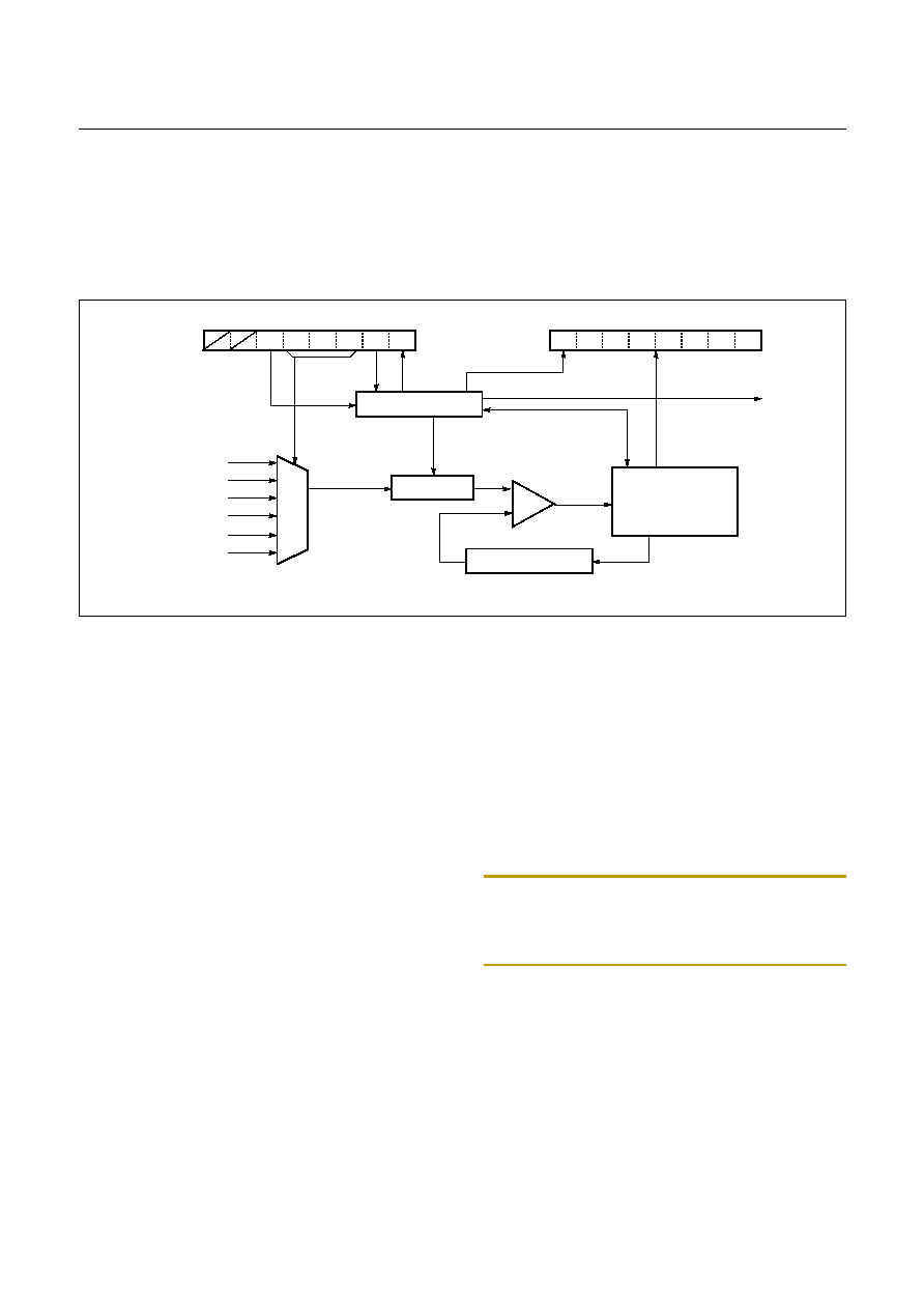
GMS81C4040/87C4060
HYUNDAI
42
May. 2000 Ver 1.0
12. A/D Converter
The A/D convertor circuit is shown in Figure 12-1 .
The A/D convertor circuit consists of the comparator and
c o n t r o l r e g i s te r A I P S ( 0 0 E F
H
) , A D C M ( 0 0 F 0
H
) ,
ADR(00F1
H
). The AIPS register select normal port or an-
alog input. The ADCM register control A/D converter's
activity. The ADR register stores A/D converted 8bit re-
sult. The more details are shown Figure 12-2 .
Figure 12-1 Block Diagram of A/D convertor circuit
Control
The GMS81C4040/GMS87C4060 contains a A/D con-
verter module which has six analog inputs.
1. First of all, you have to select analog input pin by set the
ADCM and AIPS.
2. Set ADEN (A/D enable bit : ADCM bit5).
3. Set ADST (A/D start bit : ADCM bit1). We recommend
you do not set ADEN and ADST at once, it makes worse
A/D converted result.
4. ADST bit will be cleared automatically 1cycle after you
set this.
Example:
:
; Set AIPS, change ? to what you want
;
0 : digital port
;
1 : analog port
LDM AIPS,#00??????b
; Set ADEN, xxx is analog port number
LDM ADCM,#001xxx00b
; or "SET1 ADEN"
; Set ADST, xxx is analog port number
LDM ADCM,#001xxx10b
; or "SET1 ADST"
:
:
5. After A/D conversion is completed, ADSF bit and inter-
rupt flag IFA will be set. (A/D conversion takes 36 ma-
chine cycle : 9uS when f
ex
=8MHz).
Note: Make sure AIPS bits, if you using a port which is set
digital input by AIPS, analog voltage will be flow into MCU
internal logic not A/D converter. Sometimes device or port
is damaged permanently.
Comparator
AN0
MUX
AN1
AN2
AN3
port
select
+
-
S/H
ADCM [F0
H
]
ADEN ADS2 ADS1 ADS0 ADST ADSF
ADR [F1
H
]
AN4
AN5
Control circuit
Register ladder
Succesive
Approximation
Circuit
IFA
Vref
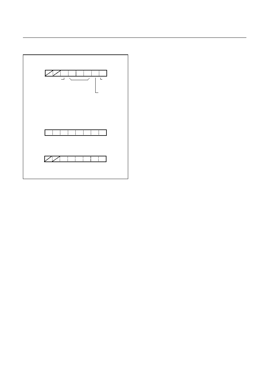
HYUNDAI
GMS81C4040/87C4060
May. 2000 Ver 1.0
43
Figure 12-2 A/D convertor Registers
A/D Result Register
ADR
ADDRESS : 00F1
H
RESET VALUE : Undefined
A/D Convertor mode Register
ADCM
ADDRESS : 00F0
H
RESET VALUE : --01 1101
b
Port Property
Analog input pin selector Register
AIPS
ADDRESS : 00EF
H
RESET VALUE : --00 0000
b
0: Digital I/O
1: Analog Input
ADEN ADS2 ADS1 ADS0 ADST ADSF
A/D Status
0: Busy
1: Finish
A/D Start
0: Ignore
1: A/D start
A/D Port select
000: AN0
001: AN1
A/D Enable
0: Disable
1: Enable
010: AN2
011: AN3
100: AN4
101: AN5
11x: No Analog port
8bit result is stored
RW
RW
RW
RW
RW
R
R
R
R
R
R
R
R
R
W
W
W
W
W
W
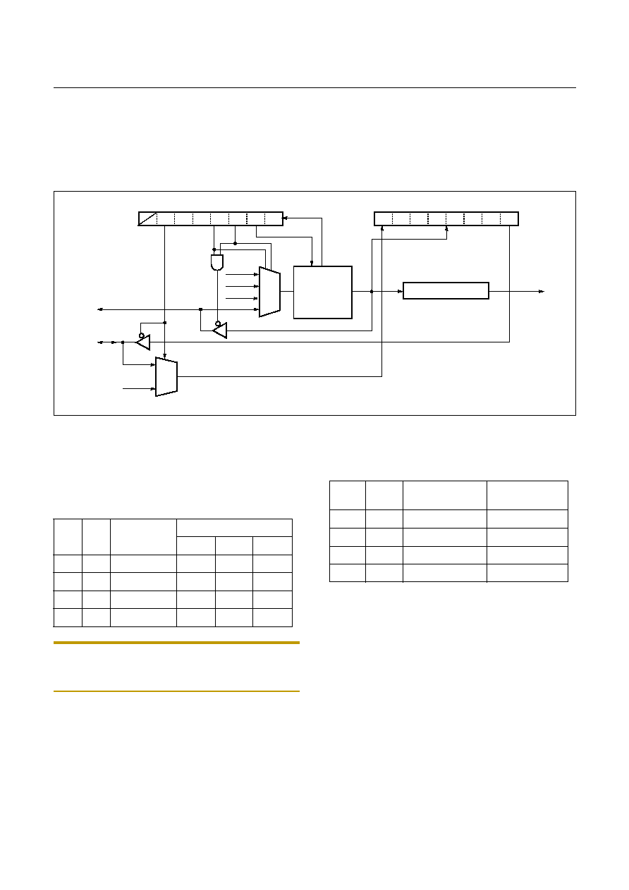
GMS81C4040/87C4060
HYUNDAI
44
May. 2000 Ver 1.0
13. Serial I/O
The Serial I/O circuit is shown in Figure 13-1 .
The Serial I/O circuit consists of the octal counter, SI-
OR(DF
H
), SIOM(DE
H
). The SIOR register stores received
data or data which will be transfered. The SIOM register
controls serial communication mode, speed, start, etc.
The more details about registers are shown Figure 13-2 .
Figure 13-1 Block Diagram of Serial I/O circuit
Control
The GMS81C4040/GMS87C4060 contains a Synchronous
type Serial I/O module.
1. You have to select serial I/O pins by set the SM1~0.
Note: Sout pin can handle serial data output or serial data
input. You can input serial data to Sout pin when IOSW bit
is 1. But Sin pin is dedicated serial data input pin.
2. You have to select serial communication clock by set the
SCK1~0.
3. If you want to send data, write it to SIOR. Or not skip
this.
4. Start serial communication by set SIOST(Serial I/O
start, SIOM bit1).
5
. After serial communication is completed, SIOSF bit and
interrupt flag IFSIO will be set.
MUX
SIOM [DE
H
]
SM1
SM0
SCK1 SCK0 SIOST SIOSF
SIOR [DF
H
]
Sout
Sin
Octal counter
Control
Circuit
IFSIO
IOSW
1
0
MUX
PS3
PS5
PS4
Exclk
Sclk
D7
D6
D5
D4
D3
D2
D1
D0
SM1
SM0
Function
Port select
R21
R22
R23
0
0
-
R21
R22
R23
0
1
Send
Sclk
Sout
R23
1
0
Receive
Sclk
R22
Sin
1
1
-
R21
R22
R23
SCK1
SCK0
Selected Clock
Ex: Frequency
(f
ex
=8MHz)
0
0
PS3
1uS
0
1
PS4
2uS
1
0
PS5
4uS
1
1
External clock
User define
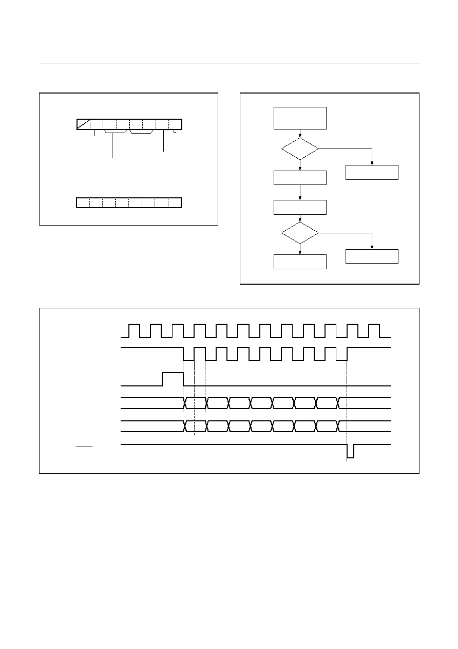
HYUNDAI
GMS81C4040/87C4060
May. 2000 Ver 1.0
45
Figure 13-2 Serial I/O Registers
Figure 13-3 Example for serial I/O check by S/W
Figure 13-4 Serial I/O Timing Chart
Serial I/O data Register
SIOR
ADDRESS : 0DF
H
RESET VALUE : Undefined
Serial I/O mode Register
SIOM
ADDRESS : 0DE
H
RESET VALUE : -000 0001
b
Serial Status
0: Busy
1: Finish
Serial COMM. Start
0: Ignore
1: COMM. start
Input select
0: Sin
1: Sout
SM1
SM0
SCK1 SCK0 SIOST SIOSF
IOSW
Clock Select
Send / Receive
D7
D6
D5
D4
D3
D2
D1
D0
RW
RW
RW
RW
RW
RW
R
RW
RW
RW
RW
RW
RW
RW
RW
Serial I/O Interrupt
Service routine
SIOSF=1?
SE=0
// SE : Interrupt enable bit
Abnormal operation
Write SIOM
SR=0?
// SR : Interrupt request flag
Normal operation
Overrun error
No
Yes
No
Yes
D0
Input clock
Sout
Sin
IFSIO
Sclk
SIOST
D1
D2
D3
D4
D5
D6
D7
D0
D1
D2
D3
D4
D5
D6
D7
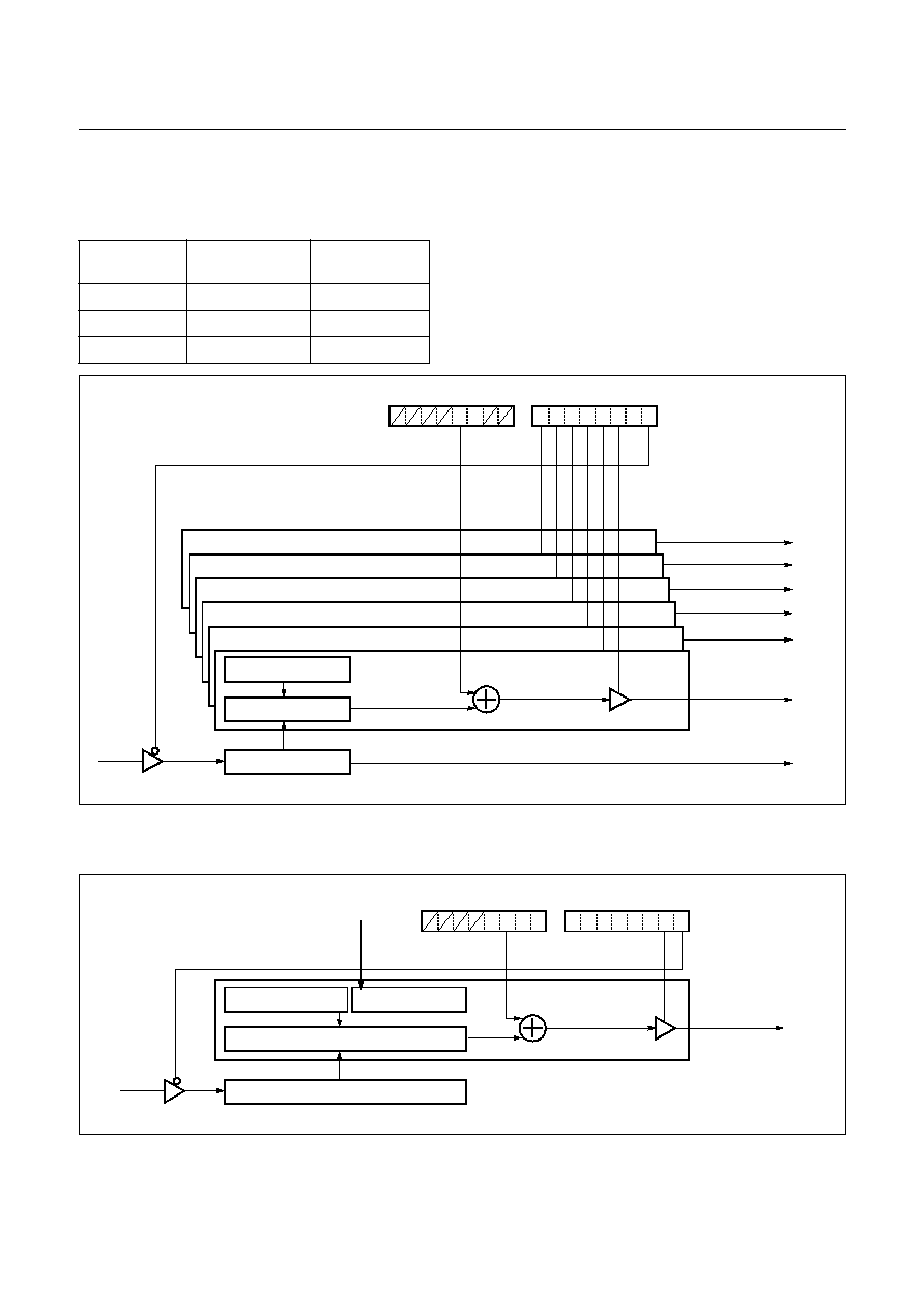
GMS81C4040/87C4060
HYUNDAI
46
May. 2000 Ver 1.0
14. Pulse Width Modulation (PWM)
The PWM circuit is shown in Figure 14-1 , Figure .
The PWM circuit consists of the counter, comparator, Data
register.
The PWM control registers are PWMR7~0, PWMCR2~1,
PWM8H, PWM8L.
The more details about registers are shown Figure 14-2 .
Figure 14-1 8bit register (PWM7~0) circuit
Figure 14-2 14bit register (PWM8) circuit
Example
(f
ex
=8MHz)
14bit PWM
8bit PWM
Resolution
0.5uS
4uS
Input Clock
2MHz
250KHz
Frame cycle
8,192uS
1,024uS
PWMCR2 [EB
H
]
8bit counter
PWM0
PWMCR1 [EA
H
]
8bit comparator
PWMR0 [E0
H
]
EN
5
EN
4
EN
3
EN
2
EN
1
EN
0
PWMR1 [E1
H
]
PWMR2 [E2
H
]
PWMR3 [E3
H
]
PWMR4 [E4
H
]
PWMR5 [E5
H
]
PWM5
PWM4
PWM3
PWM2
PWM1
IF1Frame
PS5
CNTB
PWMCR2 [EB
H
]
14bit counter
PWM8
PWMCR1 [EA
H
]
14bit comparator
PWMR8H 8bit [E8
H
]
EN
8
PS2
CNTB
PWMR8L 6bit [E9
H
]
MSB
LSB
Inter
nal
C
ontr
o
l
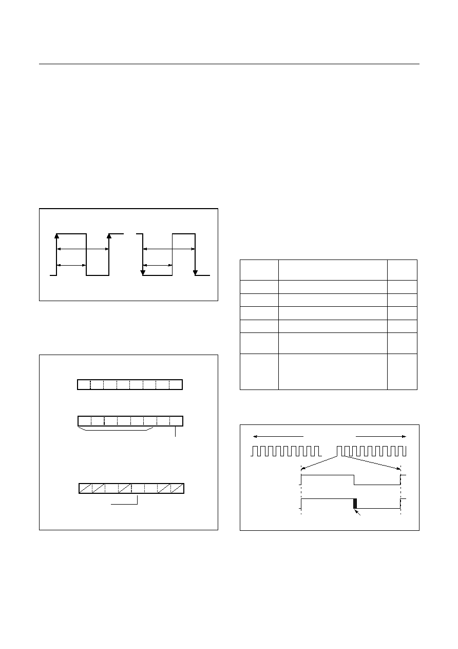
HYUNDAI
GMS81C4040/87C4060
May. 2000 Ver 1.0
47
8bit PWM Control
The GMS81C4040/GMS87C4060 contains a one 14bit
PWM and six 8bit PWM module.
1. 8bit PWM0~5 is wholy same internal circuit, but
PWM0~5 output port is NMOS open drain.
2. Al l PWM polarity has the same by POL2's value.
3. Calulate Frame cycle and Pulse width is as following.
PWM Frame Cycle = 2
13
/ f
ex
(Sec)
PWM Width = (PWMRn+1) * 2
5
/ f
ex
(n=0~5)
Pulse Duty (%) = (PWMRn +1) / 256 *100(%) (n=0~5)
Figure 14-3 Wave form example for 8bit PWM
4. PWM output is enabled during ENn(n=0~5) bit (See
PWMCR1~2) contains 1.
Figure 14-4 8bit PWM Registers
5. CNTB controls all PWM counter enable.
If CNTB=0, Counter is enabled.
14bit PWM Control
1. 14bit PWM's operation concept is not the same as 8bit
PWM.
1 PWM frame contains 64 sub PWMs.
PWM8H : Set sub PWM's basic Pulse Width.
PWM8L : Number of sub PWM which is added 1 clock.
2. PWM polarity is selected by POL1's value.
If POL1=0, Positive Polarity.
3. Calulate Frame cycle and Pulse width is as following.
Main PWM Frame Cycle = 2
16
/ f
ex
(Sec).
Sub PWM Frame Cycle = Main Frame Cycle / 64.
4. Table 14-1, "PWM8L and Sub frame matching table,"
on page 47 show PWM8L function.
Figure 14-5 Wave form example for 14bit PWM
Positive Polarity (POL2=0)
1
2
Negative Polarity (POL2=1)
1
2
1. Frame cycle
2. Pulse Width
PWM Data Register
PWMR0~5
ADDRESS : 0E0~E5
H
RESET VALUE : Undefined
D7
D6
D5
D4
D3
D2
D1
D0
EN5,4,3,2,1 : R47,45,43,42,41,40
PWM control Register 1
PWMCR1
ADDRESS : 0EA
H
RESET VALUE : 0000 0000
b
0: R4x acts normal digital port
1: R4x acts PWM output port
EN2
EN1
EN0
EN8
CNTB
EN3
EN4
EN5
PWM control Register 2
PWMCR2
ADDRESS : 0EB
H
RESET VALUE : --0- 00--
b
POL2 POL1
BUZS
8bit PWM Polarity
0: Positive (PWM from Rising edge)
1: Negative (PWM from Rising edge)
14bit Counter enable
0: Counter run
1: Counter stop
W
W
W
W
W
W
W
W
RW
RW
RW
RW
RW
RW
RW
RW
RW
RW
RW
Bit value
Sub frame number which is
added 1 clock
Pulse
count
if Bit0=1
32
1
if Bit1=1
16, 48
2
if Bit2=1
8, 24, 40, 56
4
if Bit3=1
4, 12, 20, 28, 36, 44, 52, 60
8
if Bit4=1
2, 6, 10, 14, 18, 22, 26, 30, 34,
38, 42, 46, 50, 54
16
if Bit5=1
1, 3, 5, 7, 9, 11, 13, 15, 17, 19,
21, 23, 25, 27, 29, 31, 33, 35, 37,
39, 41, 43, 45, 47, 49, 51, 53, 55,
57, 59, 61, 63
32
Table 14-1 PWM8L and Sub frame matching table
Main PWM Frame
.....
0
1 2
61 62 63
Sub PWM Frame
Sub PWM Frame
which is added
1 clock
1 clock width : PS2
GMS81C4040/87C4060
HYUNDAI
48
May. 2000 Ver 1.0
Figure 14-6 14bit PWM Registers
5. PWM output is enabled during EN8 bit contains 1.
6. CNTB controls PWM counter enable.
If CNTB=0, Counter is enabled.
PWM Width Data Register
ADDRESS : 0E8
H
RESET VALUE : Undefined
D7
D6
D5
D4
D3
D2
D1
D0
PWM Sub-pulse count Register
PWM8L
ADDRESS : 0E9
H
RESET VALUE : Undefined
PWM control Register 2
PWMCR2
ADDRESS : 0EB
H
RESET VALUE : --0- 00--
b
POL2
POL1
BUZS
14bit PWM Polarity
0: Positive (PWM from Rising edge)
1: Negative (PWM from Rising edge)
PWM8H
D5
D4
D3
D2
D1
D0
PWM control Register 1
PWMCR1
ADDRESS : 0EA
H
RESET VALUE : 0000 0000
b
EN2
EN1
EN0
EN8
CNTB
EN3
EN4
EN5
14bit Counter enable
0: Counter run
1: Counter stop
14bit PWM enable
0: R51
1: PWM8
RW
RW
RW
RW
RW
RW
RW
RW
RW
RW
RW
RW
RW
RW
RW
RW
RW
RW
RW
RW
RW
RW
RW
RW
RW
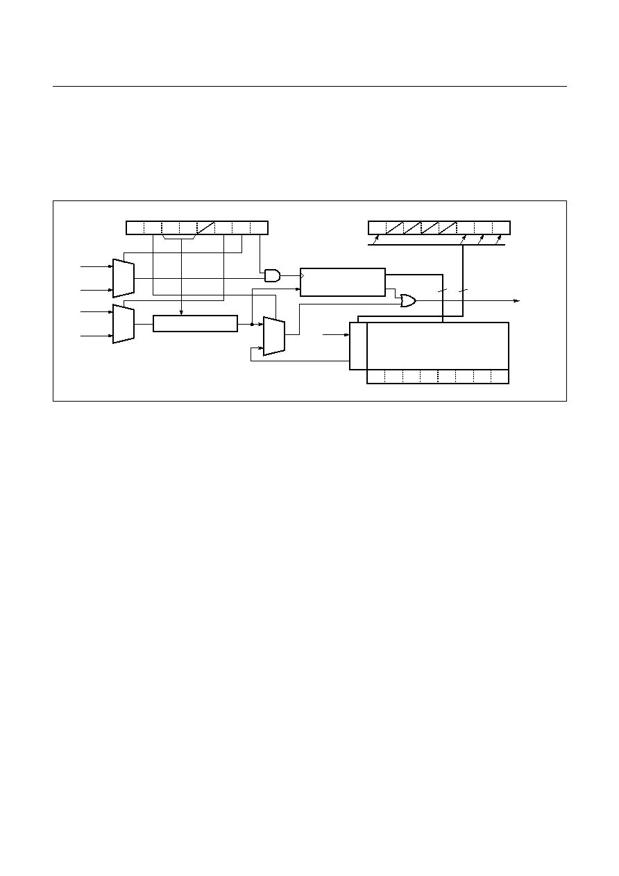
HYUNDAI
GMS81C4040/87C4060
May. 2000 Ver 1.0
49
15. Interrupt interval measurement circuit
The Interrupt interval measurement circuit is shown in Fig-
ure 15-1 .
The Interrupt interval measurement circuit consists of the
input multiplexer, sampling clock multiplexer, Edge detec-
tor, 8bit counter, measured result storing register, FIFO
(9bit, 6level) interrupt, Control register, etc.
The more details about registers are shown Figure 15-2 .
Figure 15-1 Block Diagram of Interrupt interval measurement circuit
Control
The GMS81C4040/GMS87C4060 contains a Interrupt in-
terval measurement module.
1. Select interrupt input pin what you want to measure by
set the FUNC1 [00CE
H
].
2. Set IDCR [00F9
H
] : FIFO clear, interrupt mode, inter-
rupt edge select, external interrupt select between INT3
and INT4, sampling clock select.
3. Set IDCR [00F9
H
] : set IDST to start measuring.
4. Counter value is stored to IDR [00FB
H
] when selected
edge is detected. After data was written, timer is cleard au-
tomatically and it counts continue.
5
. You can select interrupt occuring point by set Interrupt
Mode Select bit (IMS), every edge what you selected or
FIFO 4 level is filled.
6. If input signal's interval is larger than maximum counter
value (0FF
H
), counter occurring an interrupt and count
again from 00
H
.
7. See Figure 15-4 FIFO operating mechanism.
MUX
IDCR [F9
H
]
I34H
I34L
ISEL
IDCK
IDST
IDFS [FA
H
]
INT3
INT4
8bit counter
FIFO
(9bit, 6level)
INTV
IMS
1
0
DPOL
FOE
FFUL FEMP
FCLR
MUX
PS8
PS9
1
0
MUX
0
1
Edge detector
Clear
IDR [FB
H
]
D7
D6
D5
D4
D3
D2
D1
D0
Overflow
8
4
FCLR
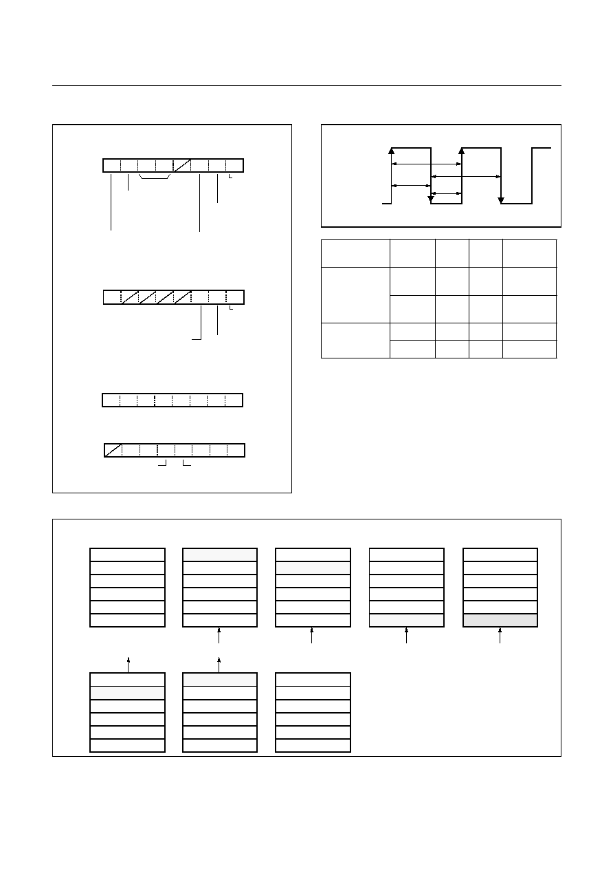
GMS81C4040/87C4060
HYUNDAI
50
May. 2000 Ver 1.0
Figure 15-2 Int. interval measurement Registers
Figure 15-3 Setting for measurement
Figure 15-4 Example for FIFO operating mechanism
IDR
ADDRESS : 00FB
H
RESET VALUE : Undefined
Interrupt interval determination
IDCR
ADDRESS : 00F9
H
RESET VALUE : 0000 -000
b
Counter control
0: stop
1: Clear & count
Sampling clock select
0: PS9
1: PS8
Int. occuring time
0: Every selected
I34H
I34L
FCLR
ISEL
IDCK
IDST
IMS
See Figure 15-3
D7
D6
D5
D4
D3
D2
D1
D0
R24/INT3
Port function select Register 1
FUNC1
ADDRESS : 00CE
H
RESET VALUE : -000 0000
b
0: R24
1: INT3
INT4S INT3S INT2S INT1S INT0S
EC2S
EC3S
control Register
External Interrupt select
0: INT3
1: INT4
FIFO clear
0: Ignored
1: Clear and return to 0
edge by I34H/L
1: Every FIFO 4level
is filled
is filled
Interrupt interval determination
IDFS
ADDRESS : 00FA
H
RESET VALUE : 1--- -001
b
FIFO Empty flag
0: Data filled
1: Empty
FIFO Full flag
0: Not full
1: Full
DPOL
FOE
FFUL
FEMP
FIFO status Register
FIFO overrun error flag
0: No Error
1: Error detected
Data polarity
0: Data is stored every Falling edge
Interrupt interval determination
FIFO Data Register
1: Data is stored every Rising edge
R26/INT4
0: R26
1: INT4
RW
RW
RW
RW
RW
RW
RW
R
R
R
R
R
R
R
R
R
R
R
R
W
W
W
W
W
W
W
Item
Symbol
I34H
I34L
Detecting
edge
Frame Cycle
1
0
Rising
edge
0
1
Falling
edge
Pulse width
1
1
Both edge
1
1
Both edge
Interrupt input
1) FIFO storing mechanism
2) FIFO reading mechanism
FEMP=1, FFUL=0
FEMP=0, FFUL=0
FEMP=0, FFUL=0
FEMP=0, FFUL=1
FEMP=0, FFUL=1
FEMP=0
FEMP=0
FEMP=1
Read out
Read out
Data in
Data in
Data in
Data in
Data 6 will be erased.
Data 1
Data 1
Data 2
Data 1
Data 2
Data 3
Data 4
Data 5
Data 6
Data 1
Data 2
Data 2
Data 1
Data 2
Data 3
Data 4
Data 5
Data 7
FOE=1 (Over run error)
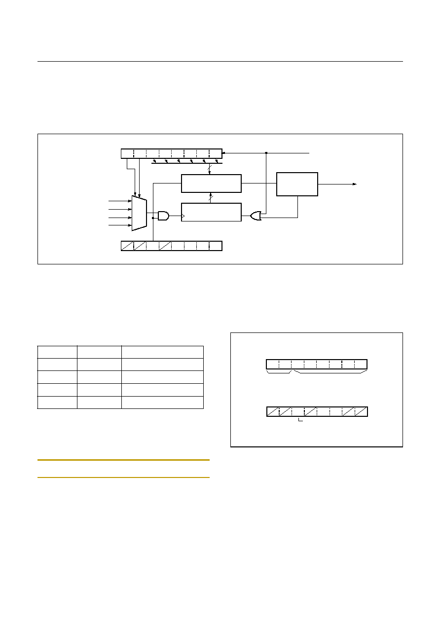
HYUNDAI
GMS81C4040/87C4060
May. 2000 Ver 1.0
51
16. Buzzer driver
The Buzzer driver circuit is shown in Figure 16-1 .
The Buzzer driver circuit consists of the 6bit counter, 6bit
comparator, Buzzer data register BUR(00EE
H
). The BUR
register controls source clock and output frequency.
The more details about registers are shown Figure 16-2 .
Figure 16-1 Block Diagram of Buzzer driver circuit
Control
The GMS81C4040/GMS87C4060 contains a Buzzer driv-
er module.
1. Selec t an input clock am ong PS4~7 by se t the
BUCK1~0 of BUR.
2. Select output frequency by change the BU5~0.
Output frequency = 1 / (PSx * BUy *2) Hz.
x=4~7, y=5~0
See example Table 16-1 and Table 16-2.
Note: Do not select 00
H
to BU5~0. It means counter stop.
3. Set BUZS bit for output enable.
4. Output waveform is rectagle clock which has 50% duty.
5. You can use this clock for the other purposes.
Figure 16-2 Buzzer driver Registers
BUR [EE
H
]
BU5
BU4
BU3
BU2
BU1
BU0
6bit counter
Output
Generator
BUZZ
BUCK
MUX
PS4
PS6
PS5
PS7
BUCK
-1
-0
00
01
10
11
clear
6bit Comparator
clear
PWMCR2 [EB
H
]
BUZS
POL2
POL1
EN7
EN6
BUR write
6
6
BUCK1
BUCK0
Clock source
0
0
PS4
0
1
PS5
1
0
PS6
1
1
PS7
Buzzer data Register
BUR
ADDRESS : 0EE
H
RESET VALUE : ???? ????
b
Input select
Clock Select
PWM control Register 2
PWMCR2
ADDRESS : 0EB
H
RESET VALUE : --0- 00--
b
POL2 POL1
BUZS
R50/Buzz select
0: R50
1: Buzz output
BU5
BU4
BU3
BU2
BU1
BU0
BUCK
BUCK
-1
-0
W
W
W
W
W
W
W
W
RW
RW
RW
GMS81C4040/87C4060
HYUNDAI
52
May. 2000 Ver 1.0
BUR5~0
Output frequency (KHz)
Dec
Hex
PS4
PS5
PS6
PS7
1
2
3
4
5
6
7
8
9
10
11
12
13
14
15
16
17
18
19
20
21
22
23
24
25
26
27
28
29
30
31
32
33
34
35
36
37
38
39
40
41
42
43
44
45
46
47
48
49
50
51
52
53
54
55
56
57
58
59
60
61
62
63
01
02
03
04
05
06
07
08
09
0A
0B
0C
0D
0E
0F
10
11
12
13
14
15
16
17
18
19
1A
1B
1C
1D
1E
1F
20
21
22
23
24
25
26
27
28
29
2A
2B
2C
2D
2E
2F
30
31
32
33
34
35
36
37
38
39
3A
3B
3C
3D
3E
3F
250
125
83.333
62.5
50
41.666
35.714
31.25
27.728
25
22.728
20.834
19.23
17.858
16.666
15.626
14.706
13.888
13.158
12.5
11.904
11.364
10.87
10.416
10
9.616
9.26
8.928
8.62
8.334
8.064
7.812
7.576
7.352
7.124
6.944
6.756
6.578
6.41
6.25
6.098
5.952
5.814
5.682
5.556
5.434
5.32
5.208
5.102
5
4.902
4.808
4.716
4.63
4.546
4.464
4.386
4.31
4.238
4.166
4.098
4.032
3.968
125
62.5
42.666
31.25
25
20.888
17.858
15.625
13.888
12.5
11.364
10.417
9.615
8.929
8.333
7.813
7.353
6.944
6.579
6.25
5.952
5.682
5.435
5.208
5
4.808
4.63
4.464
4.31
4.167
4.032
3.906
3.788
3.676
3.571
3.472
3.378
3.289
3.205
3.125
3.049
2.976
2.907
2.841
2.778
2.717
2.66
2.604
2.551
2.5
2.451
2.404
2.358
2.315
2.273
2.232
2.193
2.155
2.119
2.083
2.049
2.016
1.984
62.5
31.25
20.833
15.625
12.5
10.461
8.928
7.813
6.944
6.25
5.682
5.209
4.808
4.484
4.166
3.906
3.676
3.472
3.289
3.125
2.976
2.841
2.718
2.604
2.5
2.404
2.315
2.232
2.155
2.084
2.016
1.953
1.894
1.838
1.786
1.736
1.689
1.645
1.602
1.563
1.524
1.488
1.453
1.421
1.389
1.359
1.33
1.302
1.276
1.25
1.225
1.202
1.179
1.157
1.136
1.116
1.096
1.078
1.059
1.042
1.025
1.008
0.992
31.25
15.625
10.436
7.813
6.25
5.208
4.464
3.907
3.472
3.125
2.841
2.604
2.404
2.242
2.083
1.953
1.838
1.736
1.644
1.562
1.438
1.420
1.359
1.302
1.25
1.202
1.158
1.116
1.078
1.042
1.008
0.976
0.947
0.919
0.893
0.868
0.845
0.822
0.801
0.781
0.762
0.744
0.727
0.710
0.694
0.679
0.665
0.651
0.638
0.625
0.613
0.601
0.590
0.579
0.568
0.558
0.548
0.539
0.530
0.521
0.512
0.504
0.496
Table 16-1 . Example for f
ex
=8MHz
BUR5~0
Output frequency (KHz)
Dec
Hex
PS4
PS5
PS6
PS7
1
2
3
4
5
6
7
8
9
10
11
12
13
14
15
16
17
18
19
20
21
22
23
24
25
26
27
28
29
30
31
32
33
34
35
36
37
38
39
40
41
42
43
44
45
46
47
48
49
50
51
52
53
54
55
56
57
58
59
60
61
62
63
01
02
03
04
05
06
07
08
09
0A
0B
0C
0D
0E
0F
10
11
12
13
14
15
16
17
18
19
1A
1B
1C
1D
1E
1F
20
21
22
23
24
25
26
27
28
29
2A
2B
2C
2D
2E
2F
30
31
32
33
34
35
36
37
38
39
3A
3B
3C
3D
3E
3F
375
187.5
125
93.75
75
62.5
53.572
46.875
41.666
37.5
34.09
31.25
28.846
26.786
25
23.436
22.058
20.833
19.736
18.75
17.858
17.045
16.304
15.625
15
14.424
13.888
13.393
12.932
12.5
12.096
11.718
11.364
11.03
10.714
10.416
10.136
9.868
9.616
9.375
9.146
8.929
8.72
8.523
8.334
8.152
7.978
7.813
7.654
7.5
7.352
7.212
7.076
6.944
6.818
6.696
6.578
6.466
6.356
6.25
6.148
6.048
5.952
187.5
93.75
62.5
46.875
37.5
31.25
26.786
23.436
20.833
18.75
17.045
15.625
14.423
13.393
12.5
11.719
11.029
10.417
9.868
9.375
8.929
8.523
8.152
7.813
7.5
7.212
6.944
6.696
6.466
6.25
6.048
5.859
5.682
5.515
5.357
5.208
5.068
4.934
4.808
4.688
4.573
4.464
4.36
4.261
4.167
4.076
3.989
3.906
3.827
3.75
3.676
3.606
3.538
3.472
3.409
3.348
3.289
3.233
3.178
3.125
3.074
3.024
2.976
93.75
46.875
31.35
23.436
18.75
15.625
13.393
11.719
10.417
9.375
8.523
7.813
7.211
6.696
6.25
5.859
5.515
5.208
4.934
4.688
4.464
4.261
4.076
3.906
3.75
3.606
3.472
3.348
3.233
3.125
3.024
2.930
2.841
2.757
2.679
2.604
2.534
2.467
2.404
2.344
2.287
2.232
2.18
2.131
2.083
2.038
1.995
1.953
1.913
1.875
1.838
1.802
1.769
1.736
1.705
1.674
1.645
1.616
1.589
1.563
1.537
1.512
1.488
46.875
23.438
15.625
11.719
9.375
7.813
6.696
5.895
5.208
4.688
4.261
3.906
3.606
3.348
3.125
2.930
2.757
2.604
2.467
2.344
2.232
2.131
2.038
1.953
1.875
1.803
1.736
1.674
1.616
1.563
1.512
1.465
1.420
1.379
1.339
1.302
1.267
1.234
1.202
1.172
1.143
1.116
1.09
1.065
1.042
1.019
0.997
0.977
0.957
0.938
0.919
0.901
0.884
0.868
0.852
0.837
0.822
0.808
0.795
0.781
0.768
0.756
0.744
Table 16-2 . Example for f
ex
=12MHz
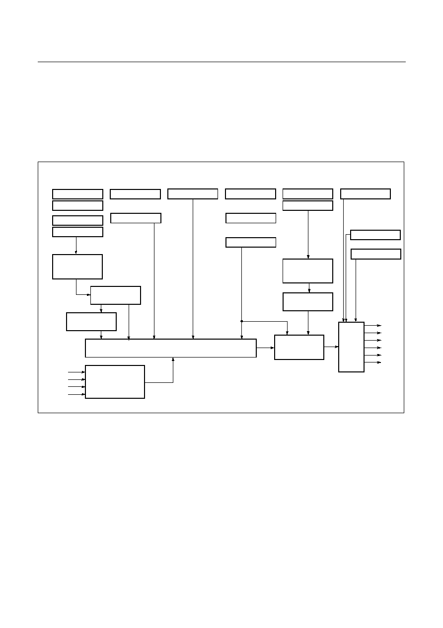
HYUNDAI
GMS81C4040/87C4060
May. 2000 Ver 1.0
53
17. On Screen Display (OSD)
The On Screen Display circuit is shown in Figure 17-1 .
The GMS81C4040/GMS87C4060 can support 512 OSD
chacters, but the last 6 characters (number 506 ~ 511,
1FA
H
~ 1FF
H
) are reserved for IC test and its pattern is
fixed by manufacturer. So you can use 506 characters for
your own.
The OSD circuit consists of the Position attribute register,
Line register, Full screen screen control register, sprite
control register, sprite position reigster, I/O polarity regis-
ter, sprite RAM, font ROM, VRAM, etc. The more details
about registers are shown Figure 17-2.
Figure 17-1 Block Diagram of On Screen Display circuit
L1ATTR [AF0
H
]
OSD Control
Circuit
OSDLN [AE5
H
]
OSDCON1 [AE0
H
]
OSDCON2 [AE1
H
]
SPVPOS [AE8
H
]
OSDPOL [AE2
H
]
Line 1,2 Attribute,
Position register
Line register
Full screen control
Sprite position register
I/O polarity register
Sprite control register
register
L1VPOS [AF1
H
]
L2ATTR [AF3
H
]
L2VPOS [AF4
H
]
SPHPOS [AE9
H
]
LHPOS [AE6
H
]
Horizontal position register
FDWSET [AE3
H
]
Field detection register
EDGECOL [AE4
H
]
Edge color register
VRAM
Font ROM
Sprite Control
Circuit
Sprite RAM
OSD, Sprite Generation Circuit
Sprite Control
Circuit
Output
Control
Circuit
Synchronization
Circuit
HSYNC
VSYNC
OSC1
OSC2
R
G
B
I
YS
YM
Color Mode Register
COLMOD [0AEF
H
]
Mesh Control Register
MESHCON [0AEB
H
]
GMS81C4040/87C4060
HYUNDAI
54
May. 2000 Ver 1.0
Figure 17-2 OSD Character Font Example
Character(foreground)
Background
Characte(foreground) Outline
Character Shadow
Background Shadow
- 16 color with half intensity
- Color selecting: VRAM n-character bit19~16(see VRAM)
- 16 color with half intensity
- Color selecting :VRAM n-character bit23-20(see VRAM)
- Controled by LnATTR register(see LnATTR)
- 16 color with half intensity
- Color selecting : EDGECOL register(see EDGECOL)
- Controlled by VRAM n-character bit15-12
- Controlled by LnATTR register(see LnATTR) and
- Color selecting : EDGECOL register(see EDGECOL)
- 16 color with half intensity
VRAM n-character bit11-10(see VRAM)
- Color selecting : EDGECOL(see EDGECOL)
- 16 color with half intensity
(No Character Outline Case)
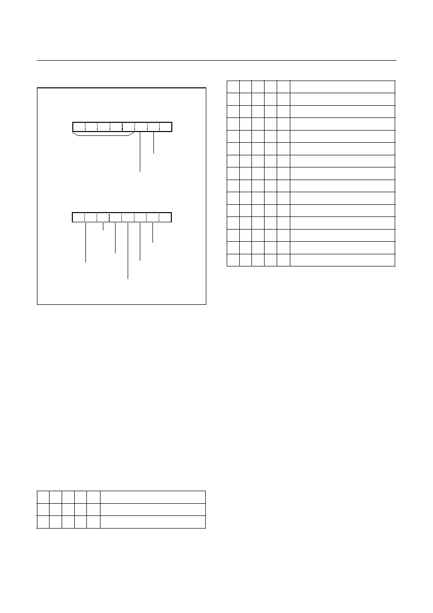
HYUNDAI
GMS81C4040/87C4060
May. 2000 Ver 1.0
55
Figure 17-3 OSD Control Registers - 1
OSDCON1
bit 0: STOCK
It controls OSD LC oscillation. If oscillation is stoped,
IC's power consumption is decreased.
bit 1: DDCLK
If you set this bit to 1, OSD input clock is doubled from LC
oscillation. It makes OSD horisontal image size as dou-
bled.
bit 2: DLINE
If you set this bit to 1, OSD vertical scan counter input
clock is doubled from normal state. It makes OSD vertical
image size as doubled.
bit 7~3: FULLM, I, B, G, R
It controls back ground color as below.
OSDCON2
bit 0: OSDON
It controls OSD, Sprite, Full screen background at once. It
does not affect anything to Vsync interrupt and OSD inter-
rupt, etc.
bit 1: PROSD
It controls screen output priority between sprite and OSD.
If its value is 1, OSD hide sprite pattern in overapped area.
bit 2: ENSP
It enables sprite display.
bit 3: DUSP
It doubles sprite's horizontal & vertical size during this
value is 1.
bit 4: ONL1
It enables OSD line 1 display. If it is enabled, OSD inter-
rupt is activated.
bit 5: ONL2
It enables OSD line 2 display. If it is enabled, OSD inter-
rupt is activated.
bit 6: OBGW
It controls character's width. Default width is 12dots. If its
value is set, 2 dots (background color) are added both left
M
I
B
G
R
Color
0
0
0
0
0
Transparent (Normal TV)
0
0
0
0
1
RED
Table 17-1 Full Screen Back ground color selection
Sprite OSD control Register
OSDCON2
ADDRESS : 0AE1
H
RESET VALUE : 0000 0000
b
Full screen control Register
OSDCON1
ADDRESS : 0AE0
H
RESET VALUE : 0000 0000
b
STOP OSD clock
0: Release
1: Stop
FULB FULG FULR DLINE DDCLKSTOCK
FULI
OBGW ONL2 ONL1 DUSP ENSP PRO
OSD
FULM
Double dot clock mode
0: Normal
1: Double
Double scan line mode
0: Normal
1: Double
Full screen background
FULLM
FULLI
FULLB
FULLG
FULLR
: Half blank
: Half intensity
: Blue
: Green
: Red
OSD, Sprite
0: All Off
1: All On
Priority
0: Sprite > OSD
1: OSD > Sprite
Sprite enable
0: Disable
1: Enable
Sprite size
0: Normal
1: Double
Background width
0: 12dots
1: 14dots
OSD line 2
0: Off
1: On
OSD line 1
0: Off
1: On
per 1 character
RW
RW
RW
RW
RW
RW
RW
RW
RW
RW
RW
RW
RW
RW
RW
DUSP
CL
RW
SD
ON
Double sprite
dot clock
(Sprite size)
0: x1, x2
1: x2, x4
0
0
0
1
0
GREEN
0
0
0
1
1
RED+GREEN
0
0
1
0
0
BLUE
0
0
1
0
1
BLUE+RED
0
0
1
1
0
BLUE+GREEN
0
0
1
1
1
RED+GREEN+BLUE (WHITE)
0
1
0
0
0
BLACK
0
1
0
0
1
Half intensity RED
0
1
0
1
0
Half intensity GREEN
0
1
0
1
1
Half intencity RED+GREEN
0
1
1
0
0
Half intensity BLUE
0
1
1
0
1
Half intensity GREEN+BLUE
0
1
1
1
1
Half intensity WHITE
1
0
0
0
0
Half BLANK
M
I
B
G
R
Color
Table 17-1 Full Screen Back ground color selection
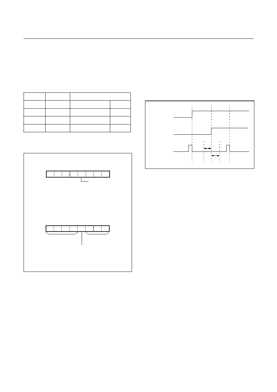
GMS81C4040/87C4060
HYUNDAI
56
May. 2000 Ver 1.0
and right side of character.
bit 7: DUSPCL
It controls sprite's dot clock and scan line speed. It does not
affect to OSD. Sprite size is controlled as below.
Figure 17-4 OSD Registers - 2
OSDPOL
bit7~0 : POL HS, VS, I, YM, YS, B, G, R
It controls HS, VS, I, YM, YS, B, G, R port's polarity. If
its value is 1, polarity is active high.
FDWSET
FDWSET (Field Detection Window Seting) register de-
tects the begin of VSync(Vertical Sync.) signal and distin-
guishs its current field is Even field or Odd field.
Figure 17-5 FDWSET detection region
The region of FMIN[2:0] ~ FMAX[3:0] is field detection
window.
FMAX[3:0] can divide the region between HSync(Hori-
zontal Sync.) by 16. You can assume there is 4 bit horizon-
tal counter, for example HCOUNT[3:0] which count 0~15.
If the start of VSync is detected at the window, next field
is even. Else if VSync is detected another region of the
window, next field is odd.
It means start of VSync is detected during FMIN[2:0] <
HCOUNT[3:0] < FMAX[3:0] and FPOL value is 0, it dis-
tinguish odd field.
And, start of VSync is detected during FMIN[2:0] <
HCOUNT[3:0] < FMAX[3:0] and FPOL value is 1, it dis-
tinguish even field.
FMIN[2:0], FMAX[3:0] are compared with the horizontal
counter in OSD block.
DUSPCL
DUSP
Size
0
0
Normal
12x16
0
1
x 2
24x32
1
0
Not used
-
1
1
x 4
48x64
Table 17-2 Sprite pattern size
I/O Polarity ( initial ) Register
OSDPOL
ADDRESS : 0AE2
H
RESET VALUE : Undefined
POL
POLI
POL
POL
POLB POLG POLR
POL
YS
YM
VS
HS
0: Active Low
1: Active High
OSD display enable,
POLHS
POLVS
POLI
POLYM
POLB
POLG
POLR
: Hsync. input
: Vsync. input
: Half intensity output
: Half blank output
: Blue output
: Green output
: Red output
include the edge color.
0: Off
1: On
Field detection Register
FDWSET
ADDRESS : 0AE3
H
RESET VALUE : 0111 1010
b
FPOL
F M IN 2 ~ 0
F M A X 3 ~ 0
Field detection polarity
0: Detect Odd field
Field detection
Maximum pointer
Field detection
Minimum pointer
Masking range : Min.~Max.
1: Detect Even field
Detecting range : Min.~Max.
W
W
W
W
W
W
W
W
W
W
W
W
W
W
W
W
HSync
Ex1: VSync(Odd)
Ex2: VSync(Even)
FMIN
FMAX
HYUNDAI
GMS81C4040/87C4060
May. 2000 Ver 1.0
57
Figure 17-6 OSD Registers - 3
Figure 17-7 OSD Registers - 4
L1ATTR
bit 0 : LIV8
It is equivalent with L1VPOS's bit 8. See more details in
L1VPOS.
bit 1: FSC1
It selects character outline and shadow color. If it is 1, it se-
lect EDGE2 color in EDGECOL register. Or not, it select
EDGE1 color. According to EDGECOL register and this
bit character and shadow colors are selected simulteneous-
ly
bit 3~2: CSZ11~CSZ10
It controls OSD character's size ( x1, x2, x3). You can use
this register and DDCLK, DLINE bit, horizontal / vertical
size can be controlled (x2, x4, x6).
bit 4: ENSH1
It enables line 1's character(foreground) shadow.
bit 5: ENOL1
It enables line 1's character(foreground) outline.
bit 6: WDSL1
It shows thickness of line 1's shadow and outline.
bit 7: OBGH1
It controls character's height. Default height is 16dots. If
its value is set, 2 dots (background color) are added both
top and bottom side of character.
OSD line Register
OSDLN
ADDRESS : 0AE5
H
RESET VALUE : ---0 0000
b
Background shadow / edge
EDGECOL
ADDRESS : 0AE4
H
RESET VALUE : Undefined
EDGnI
EDG
Edge 2 color
V L R 4 ~ 0
color Register
2I
EDG
2B
EDG
2G
EDG
2R
EDG
1I
EDG
1G
EDG
1R
EDG
1B
Edge 1 color
EDGnB
EDGnG
EDGnR
: Half Intensity
: Blue
: Green
: Red
n : 1 ~ 2
Current displayed OSD line number
( 00000 ~ 11111
b
: 0 ~ 63 )
OSD line horizontal
LHPOS
ADDRESS : 0AE6
H
RESET VALUE : Undefined
OSD line's horizontal position (00 ~ FF
H
)
Sprite vertical
SPVPOS
ADDRESS : 0AE8
H
RESET VALUE : Undefiend
Sprite horisontal
SPHPOS
ADDRESS : 0AE9
H
RESET VALUE : Undefined
position Register
position Register
position Register
D7
D6
D5
D4
D3
D2
D1
D0
D7
D6
D5
D4
D3
D2
D1
D0
D7
D6
D5
D4
D3
D2
D1
D0
Sprite's vertical position (00 ~ FF
H
)
Sprite's horisontal position (00 ~ FF
H
)
W
W
W
W
W
W
W
W
R
R
R
R
R
W
W
W
W
W
W
W
W
W
W
W
W
W
W
W
W
W
W
W
W
W
W
W
W
OSD line 1's
L1VPOS
ADDRESS : 0AF1
H
RESET VALUE : Undefined
OSD line 1's
L1ATTR
ADDRESS : 0AF0
H
RESET VALUE : Undefined
Vertical position
Foreground shadow
ENOL ENSH
CSZ
CSZ
FSC1
L1V8
WDSL
Character size
L1V7
L1V6
L1V5
L1V4
L1V3
L1V2
L1V1
L1V0
attribute Register
vertical position Register
OSD line 1's vertical position (include L1V8 : 000 ~ 1FF
H
)
OBGH
1
1
1
1
11
10
L1VPOS's bit8
out line color
0: Edge 1's color
1: Edge 2's color
00: Normal
01: 2 times
10: 3 times
11: Reserved
Character Shodow
0: Disable
1: Enable
charcater outline
0: Disable
1: Enable
Shadow / Outline
0: 1dot
1: Propotional
Character
0: 16dots
1: 18dots
background
height
width
to character
size
W
W
W
W
W
W
W
W
W
W
W
W
W
W
W
W
control
control
WDSL
ENOL
ENSH
outline, shadow
0
0
0
No outline, No shadow
0
0
1
Thin shadow
0
1
0
Thin outline
0
1
1
Thin outline
Thick shadow
1
0
0
No outline, No shadow
1
0
1
Thick shadow
1
1
0
Thick outline
1
1
1
Thick outline
Thick shadow
Table 17-3 Character Outline, Shadow table
GMS81C4040/87C4060
HYUNDAI
58
May. 2000 Ver 1.0
L1VPOS
It shows OSD line 1's vertical position in 9bit format
(LIV8 + L1VPOS, 000 ~ 1FF
H
).
Figure 17-8 OSD Registers - 5
Figure 17-9 OSD Register - 6
L2ATTR
It controls OSD line 2's attributes. Its function is the same
as L1ATTR.
L2VPOS
It shows OSD line 2's vertical position. Its function is the
same as L1VPOS.
COLMOD
It controls OSD output mode-RGB direct half intencity.
Figure 17-10 OSD Register - 7
bit 0: C16EN
It enables RGB port half intencity output. When this bit is
set, RGB port generates half intencity output. Half intenci-
ty output is 3.5V voltage level output of RGB port. When
you use this bit, you must fill all the other bit with `0'.
Note: When you do not use RGB direct half intncsity out-
put , please initialize this register as 00h.
MESHCON
It controls OSD mesh mode color.
Figure 17-11 OSD Register - 8
Note: Please initialize this register as 00h. Though this
register is for mesh mode color, it is not used currently.
VRAM
VRAM contains 1 OSD line, 24 character's attributes.
Each character's attribute is constructed with 3 bytes, it
contains color data for background, shadow, outline, char-
acter and character number ( 000
H
~ 1FF
H
, 512 characters
OSD line 2's
L2VPOS
ADDRESS : 0AF4
H
RESET VALUE : Undefined
OSD line 2's
L2ATTR
ADDRESS : 0AF3
H
RESET VALUE : Undefined
Vertical position
Foreground shadow
ENOL ENSH
CSZ
CSZ
FSC2
L2V8
WDSL
Character size
L2V7
L2V6
L2V5
L2V4
L2V3
L2V2
L2V1
L2V0
attribute Register
vertical position Register
OSD line 2's vertical position (include L2V8 : 000 ~ 1FF
H
)
OBGH
2
2
2
2
21
20
L2VPOS's bit8
out line color
0: Edge 1's color
1: Edge 2's color
00: Normal
01: 2 times
10: 3 times
11: Reserved
Shodow control
0: Disable
1: Enable
Out line control
0: Disable
1: Enable
Shadow / Outline
0: 1dot
1: Propotional
Character
0: 16dots
1: 18dots
background
height
width
to character
size
W
W
W
W
W
W
W
W
W
W
W
W
W
W
W
W
OSD line 2's
L2VPOS
ADDRESS : 0AF4
H
RESET VALUE : Undefined
OSD line 2's
L2ATTR
ADDRESS : 0AF3
H
RESET VALUE : Undefined
Vertical position
Foreground shadow
ENOL ENSH
CSZ
CSZ
FSC2
L2V8
WDSL
Character size
L2V7
L2V6
L2V5
L2V4
L2V3
L2V2
L2V1
L2V0
attribute Register
vertical position Register
OSD line 2's vertical position (include L2V8 : 000 ~ 1FF
H
)
OBGH
2
2
2
2
21
20
L2VPOS's bit8
out line color
0: Edge 1's color
1: Edge 2's color
00: Normal
01: 2 times
10: 3 times
11: Reserved
Shodow control
0: Disable
1: Enable
Out line control
0: Disable
1: Enable
Shadow / Outline
0: 1dot
1: Propotional
Character
0: 16dots
1: 18dots
background
height
width
to character
size
W
W
W
W
W
W
W
W
W
W
W
W
W
W
W
W
Color Output Mode
COLMOD
ADDRESS : 0AEF
H
RESET VALUE : Undifined
RGB Half intensity enable
C16EN
Register
W
1: Enable
0: Enable
(see Note)
Fill with `0'
Mesh Mode Color
MESHCON
ADDRESS : 0AEB
H
RESET VALUE : See Note
Register
HYUNDAI
GMS81C4040/87C4060
May. 2000 Ver 1.0
59
), etc.
Note: if (BSL = 1) & (BSCUL = 0) & (LnATTR,ENSHn = 1),
then the right bottom shadow of font character is shifted to
1 dot right side. This shadow effect will continue until that
(BSR) of adjacent character attribution become (BSR = 1).
Line
No.
Character
No.
Address (bit 23~0)
Hexa decimal
1
1
A40
A20
A00
2
A41
A21
A01
3
A42
A22
A02
:
:
:
:
22
A55
A35
A15
23
A56
A36
A16
24
A57
A37
A17
2
1
AC0
AA0
A80
2
AC1
AA1
A81
3
AC2
AA2
A82
:
:
:
:
22
AD5
AB5
A95
23
AD6
AB6
A96
24
AD7
AB7
A97
Table 17-4 VRAM memory map
Bit No.
Name
Function
15
BSR
Enable right side background
shadow.
cf. If BSL=1 and BSCUL=1 and
LnATTR.ENSHn=1, character's
right bottom shadow is shifted to
right side by 1dot unit.
It acts continued until current
character's right side chacter's
BSR is set to 1.
14
BSL
Enable left side background
shadow.
13
BSD
Enable bottom side background
shadow.
12
BSU
Enable top side background
shadow.
11
BSCDR
Select color of right and bottom
side shadow of the background
0: Edge1, 1: Edge2 color
Table 17-5 VRAM (bit15~0) function
10
BSCUL
Select color of left and top side
shadow of the background
0: Edge1, 1: Edge2 color
9
ENRND
Enable character's rounding
8~0
CG8~0
Character font number
( among 000 ~ 1FF
H
)
Bit No. &
Name
Output ( Polarity :
Through)
Character
color
19
18
17
16
I
B
G
R
Y
M
Y
S
I
B
G
R
0
0
0
0
0
0
0
0
0
0
Clear
0
0
0
1
0
1
0
0
0
1
Red
0
0
1
0
0
1
0
0
1
0
Green
0
0
1
1
0
1
0
0
1
1
Yellow
0
1
0
0
0
1
0
1
0
0
Blue
0
1
0
1
0
1
0
1
0
1
Magenta
0
1
1
0
0
1
0
1
1
0
Cyan
0
1
1
1
0
1
0
1
1
1
White
1
0
0
0
0
1
0
0
0
0
Black
1
0
0
1
0
1
0
0
0
1
Half-I,Red
1
0
1
0
0
1
0
0
1
0
Half-I,Green
1
0
1
1
0
1
0
0
1
1
Half-I,
Yellow
1
1
0
0
0
1
0
1
0
0
Half-I,Blue
1
1
0
1
0
1
0
1
0
1
Half-I,
Magenta
1
1
1
0
0
1
0
1
1
0
Half-I,Cyan
1
1
1
1
0
1
0
1
1
1
Half-I,White
Table 17-6 VRAM (bit19~16) function
Bit No.
Name
Function
Table 17-5 VRAM (bit15~0) function
GMS81C4040/87C4060
HYUNDAI
60
May. 2000 Ver 1.0
Font ROM
The GMS81C4040/GMS87C4060 OSD character size is
fixed as 12dots (Horisontal) * 16dots (Vertical).
1. Each horisontal data (12dots) needs 2byte ROM.
2. One character is constructed with 16 horisontal data to
vertically. As a result, one character needs 32bytes (2 * 16
bytes).
3. GMS81C4040/GMS87C4060 contains 512 characters.
Total Font ROM memory size is calulated as 16,384bytes
( 32bytes / character * 512 character )
4. Font ROM memory is located from 10000
H
~ 13FFF
H
,
this memory can not be accessed by user program.
5. A character's address and dot position in font ROM is
described in Figure 17-12 .
Figure 17-12 Example for a character (53
H
)
Sprite RAM
The GMS81C4040/GMS87C4060 contains a 32bytes
(12dot * 16dot) sprite RAM.
1. In view point, sprite is similar to character font but it is
not using font ROM.
2. You can selct color by dot unit.
3. Using above 1 and 2, you can make any of patterns what
you want by software. For example, arrow cursor or some-
Bit No. &
Name
Output ( Polarity :
Through)
Back
ground
color
23
22
21
20
I
B
G
R
Y
M
Y
S
I
B
G
R
0
0
0
0
0
0
0
0
0
0
Clear
0
0
0
1
0
1
0
0
0
1
Red
0
0
1
0
0
1
0
0
1
0
Green
0
0
1
1
0
1
0
0
1
1
Yellow
0
1
0
0
0
1
0
1
0
0
Blue
0
1
0
1
0
1
0
1
0
1
Magenta
0
1
1
0
0
1
0
1
1
0
Cyan
0
1
1
1
0
1
0
1
1
1
White
1
0
0
0
1
0
0
0
0
0
Half
blanking
1
0
0
1
0
1
1
0
0
1
Half-I,Green
1
0
1
0
0
1
1
0
1
0
Half-I,
Yellow
1
0
1
1
0
1
1
0
1
1
Half-I,Blue
1
1
0
0
0
1
1
1
0
0
Half-I,
Magenta
1
1
0
1
0
1
1
1
0
1
Half-I,Cyan
1
1
1
0
0
1
1
1
1
0
Half-I,White
1
1
1
1
0
1
0
1
1
1
Black
Table 17-7 VRAM (bit 23 ~ 20) function
Charact
er code
Address range
Upper 4bit
Lower 8bit
000
H
12000
H
~ 1200F
H
10000
H
~ 1000F
H
001
H
12010
H
~ 1201F
H
10010
H
~ 1001F
H
002
H
12020
H
~ 1202F
H
10020
H
~ 1002F
H
:
:
:
xyz
H
(12000H + xyz0H) ~
(12000H + xyzFH)
(10000H + xyz0H) ~
(10000H + xyzFH)
:
:
:
1FD
H
13FD0
H
~ 13FDF
H
11FD0
H
~ 11FDF
H
1FE
H
13FE0
H
~ 13FEF
H
11FE0
H
~ 11FEF
H
1FF
H
13FF0
H
~ 13FFF
H
11FF0
H
~ 11FFF
H
Table 17-8 Font ROM memory map
MSB
LSB
Address
12530
H
12531
H
12532
H
12533
H
12534
H
12535
H
12536
H
12537
H
12538
H
12539
H
1253A
H
1253B
H
1253C
H
1253D
H
1253E
H
1253F
H
00
H
07
H
08
H
08
H
08
H
09
H
0B
H
08
H
08
H
08
H
08
H
08
H
08
H
08
H
07
H
00
H
Data
Address
10530
H
10531
H
10532
H
10533
H
10534
H
10535
H
10536
H
10537
H
10538
H
10539
H
1053A
H
1053B
H
1053C
H
1053D
H
1053E
H
1053F
H
00
H
FE
H
01
H
61
H
F1
H
F9
H
FD
H
61
H
61
H
61
H
61
H
61
H
61
H
01
H
FE
H
00
H
Data
HYUNDAI
GMS81C4040/87C4060
May. 2000 Ver 1.0
61
thing.
4. Sprite position is controlled by sprite position register
SPVPOS[0AE8
H
] and SPHPOS[0AE9
H
].
5. Sprite RAM is located 0C00~0CF5
H
. One sprite RAM
byte contains 2 dot's color data. See more details in Table
17-9 ~ Table 17-11.
Test Font
GMS81C4040 use first OSD font as test purpose(see
Fig17-13). When you design OSD characte font, you incert
following font to Font ROM 00h. If you like to use this font
originally, please contact us
Figure 17-13 Test Font Pattern
Column
number
Row number
MSB
~
LSB
00
H
0C05
H
~
0C00
H
01
H
0C15
H
~
0C10
H
02
H
0C25
H
~
0C20
H
:
:
~
:
0n
H
(n=0~F)
0Cn5
H
~
0Cn0
H
:
:
~
:
0E
H
0C05
H
~
0C00
H
0F
H
0C05
H
~
0C00
H
Table 17-9 Sprite RAM address map
Odd dot color
Even dot color
bit No.
7
6
5
4
3
2
1
0
Function
-
B
G
R
-
B
G
R
Table 17-10 A sprite RAM's contents
B
G
R
Color
0
0
0
Clear
0
0
1
Red
0
1
0
Green
0
1
1
Yellow
1
0
0
Blue
1
0
1
Black
1
1
0
Cyan
1
1
1
White
Table 17-11 Sprite RAM Color Table
1000H 00H
1001H 00H
1002H 00H
1003H F8H
1004H FCH
1005H 0EH
1006H 06H
1007H 06H
1008H 06H
1009H 06H
100AH 06H
100BH 06H
100CH 0EH
100DH FCH
100EH F8H
100FH 00H
1200H 00H
1201H 00H
1202H 00H
1203H 01H
1204H 03H
1205H 07H
1206H 06H
1207H 06H
1208H 06H
1209H 06H
120AH 06H
120BH 06H
120CH 07H
120DH 03H
120EH 01H
120FH 00H
MSB
LSB address data
address data
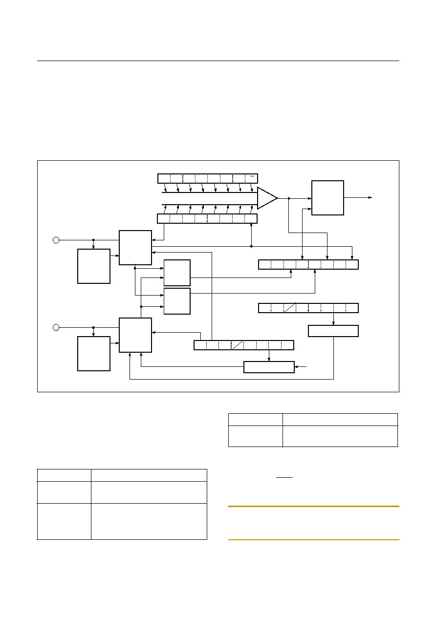
GMS81C4040/87C4060
HYUNDAI
62
May. 2000 Ver 1.0
18. I
2
C Bus Interface
The I
2
C Bus interface circuit is shown in Figure 18-1 .
The multi-master I
2
C Bus interface is a serial communica-
tions circuit, conforming to the Phlips I
2
C Bus data trans-
fer format. This interface, offering both arbitration lost
detection and a synchronous functions, is useful for the
multi-master serial communications.
This multi-master I
2
C Bus interface circuit consists of the
I
2
C address register, the I
2
C data shift register, the I
2
C
clock control register, the I
2
C control register, the I
2
C sta-
tus register and other control circuits.
The more details about registers are shown Figure 18-2 ~
Figure 18-6 .
Figure 18-1 Block Diagram of multi-master I
2
C circuit
Control
The GMS81C4040/GMS87C4060 contains two I
2
C Bus
interface modules. It supports multi-master function, so it
contains arbitration lost detection, synchronization func-
tion,etc.
I
2
C address register
It contains slave address (7bit) which is used during slave
mode and Read/Write bit.
Bit 7 ~ 0 : Slave address 6~0
Note: Bit 7~0 (SAD6~0) store slave address. The address
data transmitted from the master is compared with the con-
tents of these bits.
ICAR [D8
H
]
IFI2CR
Bit counter
SCL
Address
comparator
ICDR [D9
H
]
D7
D6
D5
D4
D3
D2
D1
D0
Interrupt
Generation
Circuit
Data
Control
Circuit
ICSR [00DA
H
]
MST
TRX
BB
PIN
AL
AAS
AD0
LRB
Noise
Elimination
Circuit
AL
Circuit
BB
Circuit
Clock
Control
Circuit
Noise
Elimination
Circuit
ICCR1 [00DB
H
]
B S E L 1 ~ 0
ALS
ESO
B C 2 ~ 0
ICCR2 [DC
H
]
ACLK ACK
1
C C R 3 ~ 0
Clock division
External clock
SDA
SAD6 SDA5 SDA4 SDA3 SDA2 SDA1 SDA0 R/W
ITEM
Function
Format
Philips
I
2
C
standard
7bit addressing format
Communication
mode
Master transmitter
Master receiver
Slave transmitter
Slave receiver
SCL clock
frequency
66.6KHz ~ 500KHz (f
ex
=12MHz)
44.4KHz ~ 333.3KHz (f
ex
=8MHz)
ITEM
Function
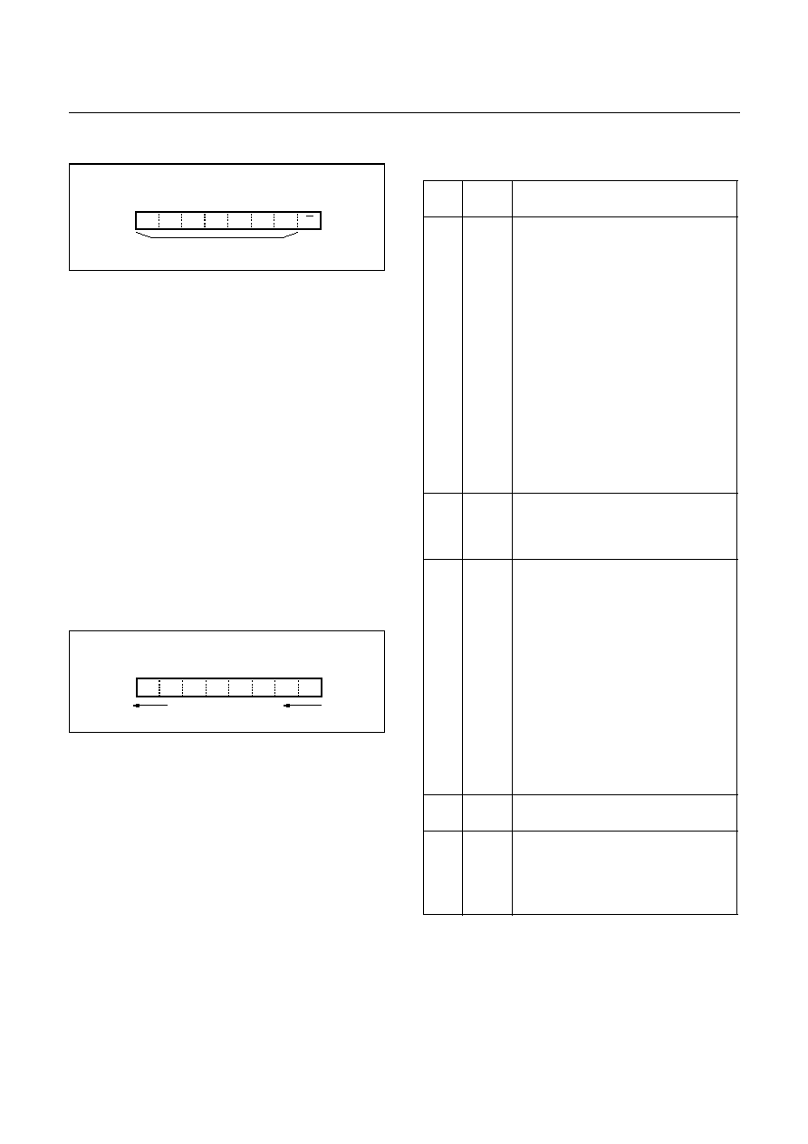
HYUNDAI
GMS81C4040/87C4060
May. 2000 Ver 1.0
63
Figure 18-2 I
2
C address Register
I
2
C data shift register [ICDR]
The I
2
C data shift register is an 8bit shift register to store
received data and write transmit data.
When transmit data is written into this register, it is trans-
fered to the outside from bit7 in synchronization with the
SCL clock, and each time one-bit data is output, the data of
this register are shifted one bit to the left. When data is re-
ceived, it is input to this register from bit0 in synchroniza-
tion with the SCL clock, and each time one-bit data is
input, the data of this register are shifted one bit to the left.
The I
2
C data shift register is in a write enable status only
when the ESO bit of the I
2
C control register (address
00DC
H
) is "1". The bit counter is reset by a write instruc-
tion to the I
2
C data shift register. Reading data from the
I
2
C data shift register is always enabled regardless of the
ESO bit value.
Figure 18-3 Data shift register
I
2
C status register
The I
2
C status register controls the I
2
C Bus interface sta-
tus. The low-order 4bits are read only bits and the high-or-
der 4bits can be read out and written to.
The more details about its bits are shown Table 18-1.
ICAR
ADDRESS : 00D8
H
RESET VALUE : 0000 0000
b
SAD6 SDA5 SDA4 SDA3 SDA2 SDA1 SDA0 R/W
Slave address
RW
RW
RW
RW
RW
RW
RW
R
ICDR
ADDRESS : 00D9
H
RESET VALUE : 0000 0000
b
RW
RW
RW
RW
RW
RW
RW
RW
D7
D6
D5
D4
D3
D2
D1
D0
S hift le ft 1-bit e ach S C L
Bit
No.
Name
Function
7
6
MST
TRX
00: Slave / Receiver mode
01: Slave / Transmitter mode
10: Master / Receiver mode
11: Master / Transmitter mode
MST is cleared when
- After reset.
- After the arbitration lost is occured and
1 byte data transmission is finished.
- After stop condition is detected.
- When start condition is disabled by
start condition duplication preventation
function.
TRX is cleared when
- After reset.
- When arbitration lost or stop condition
is occured .
- When MST is `0', and start condition
or ACK non-return mode is detected.
5
BB
BB(Bus busy)bit is 1 during bus is busy.
This bit can be written by S/W. its value
is `1' by start condition, and cleared by
stop condition.
4
PIN
PIN(Pending Interrupt Not)bit is inter-
rupt request bit.
If I
2
C interrupt request is issued, its
value is 0.
PIN is cleared when
- After 1 byte trasmission / receive is fin-
ished.
PIN is set when
- After reset.
- After write instruction is excuted into
I
2
C data shift register ICDR.
- When PIN bit low, the output of SCL is
pulled down, So if you want to release
SCL, you must perform write instruction
CDR.
3
AL
Arbitration lost detection flag.
If arbitration lost is detected, AL=1, or 0.
2
AAS
Slave address comparison flag.
It shows compared result with received
address data and I
2
C address register
(ICAR).
It is 1, when two of data is same.
Table 18-1 Bit function
GMS81C4040/87C4060
HYUNDAI
64
May. 2000 Ver 1.0
Figure 18-4 I
2
C status Register
I
2
C control register 1
It controls communication data format.
Figure 18-5 I
2
C control Register 1
I
2
C control register 2
It controls SCL mode, SCL frequency, etc.
It contains 8bit data to transmit to external device when tr-
asmitter mode, or received 8bit data from external device
when receive mode.
1
AD0
General call detection flag.
If general call is detected, AD0=1, or
not 0.
* General call : If received address is all
`0' . it is called general call.
0
LRB
Last received bit.
it is used for receive confirmation. If
ACK is returned, LRB=0, or not 1.
Bit
No.
Name
Function
7
6
BSEL1
BSEL0
I
2
C connection control.
00: No connection
01: SCL1, SDA1
10: SCL2, SDA2
11: SCL1, SDA1, SCL2, SDA2
4
ALS
Data format selection.
0: Addressing format
1: Free data format
3
ESO
I
2
C Bus interface use enable flag
0: Disabled
1: Enabled
2
BC2
Bit counter.
000
b
: 8bit
001
b
~111
b
: 1~7bit
1
BC1
0
BC0
Table 18-2 Bit function
Bit
No.
Name
Function
Table 18-1 Bit function
ICSR
ADDRESS : 00DA
H
RESET VALUE : 0001 0000
b
RW
RW
RW
RW
R
R
R
R
MST
TRX
BB
PIN
AL
AAS
AD0
LRB
Bit
No.
Name
Function
7
ACLK
Select acknowledge clock (ACK) mode.
0: No acknowledge clock mode.
acknowledge clock is not generated
after data was transmismitted.
1: acknowledge clock mode.
acknowledge clock is generated after
data was transmismitted.
6
ACK
If acknowledge clock is returned, this bit
is 0. Or not 1.
5
1
(fixed)
Not used.
Table 18-3 Bit function
ICCR1
ADDRESS : 00DB
H
RESET VALUE : 00-0 0000
b
ALS
ESO
BC2
BC1
BC0
BSEL
BSEL
1
0
RW
RW
RW
RW
RW
RW
RW
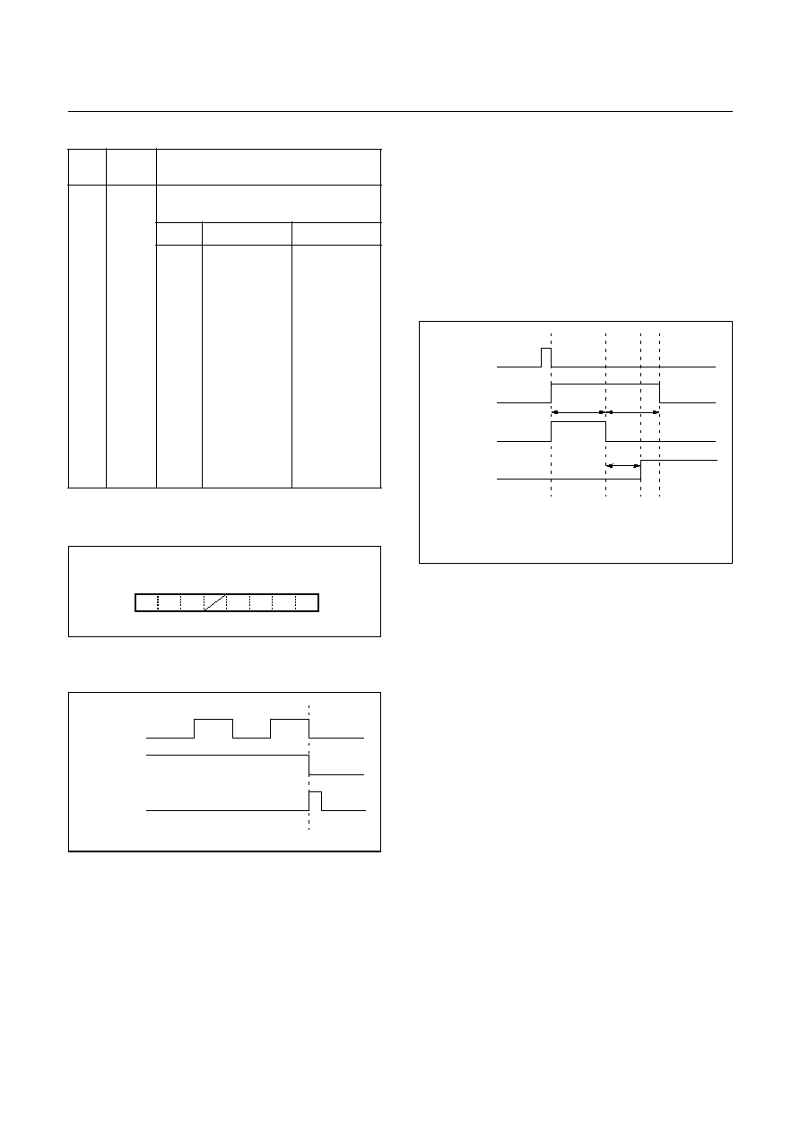
HYUNDAI
GMS81C4040/87C4060
May. 2000 Ver 1.0
65
Figure 18-6 I
2
C control Register 2
Figure 18-7 Interrupt request signal generation timing
START condition generation
When the ESO bit of the I
2
C control register (00DB
H
) is
"1", writing to the I
2
C status register will generate START
condition. Refer to Figure 18-8 for the START condition
generation timing diagram.
Figure 18-8 START condition generation timing
RESTART condition generation
RESTART condition's setting sequence is as followings.
1. Write 020
H
to I
2
C status register (ICSR, 00DA
H
)
2. Write slave address to I
2
C data shift register (ICDR,
00D9
H
)
3. Write 0F0
H
to I
2
C status register (ICSR, 00DA
H
)
STOP condition generation
Writing `C0h' to ICSR will generate a stop condition,
3
2
1
0
CCR3
CCR2
CCR1
CCR0
SCL Frequency selection
SCL frequency = f
ex
/ (12 * CCR)
Value
f
ex
= 12MHz
f
ex
= 8MHz
0000
0001
0010
0011
0100
0101
0110
0111
1000
1001
1010
1011
1100
1101
1110
1111
Not allowed
Not allowed
500.0KHz
333.3KHz
250.0KHz
200.0KHz
166.6KHz
142.9KHz
125.0KHz
111.1KHz
100.0KHz
90.0KHz
83.3KHz
76.4KHz
71.4KHz
66.6KHz
Not allowed
Not allowed
333.3KHz
222.2KHz
166.6KHz
133.3KHz
111.1KHz
95.2KHz
83.3KHz
74.1KHz
66.6KHz
60.6KHz
55.5KHz
51.3KHz
47.6KHz
44.4KHz
Bit
No.
Name
Function
Table 18-3 Bit function
ICCR2
ADDRESS : 00DC
H
RESET VALUE : 000- 0000
b
RW
RW
RW
RW
RW
RW
ACLK
ACK
1
CCR3 CCR2
CCR1 CCR0
SCL
PIN
I
2
C Request
ICSR write signal
SCL
SDA
BB (Bus busy) flag
t
SETUP
t
HOLD
t
BB
: Setup time
: Hold time
: Set time for BB
t
SETUP
t
HOLD
t
BB
(I
2
C status reg.)
GMS81C4040/87C4060
HYUNDAI
66
May. 2000 Ver 1.0
when ESO (ICCR bit3) is `1'
Figure 18-9 STOP condition generating timing diagram
START / STOP condition generation time is shown Table
18-4.
START / STOP condition detect
START / STOP condition is detected when Table 18-4 is
satisfied.
Figure 18-10 START / STOP condition detection timing
START / STOP detection time is showed Table 18-5.
ITEM
Timing SPEC.
Setup time
( t
SETUP
)
3.3uS (n=20cycles)
Hold time
( t
HOLD
)
3.3uS (n=20cycles)
Set/Reset time for
BB flag ( t
BB
)
3.0uS (n=18cycles)
Table 18-4 Example time ( f
ex
=12MHz )
ICSR write signal
SCL
SDA
BB (Bus busy) flag
t
SETUP
t
HOLD
t
BB
: Setup time
: Hold time
: Set time for BB
t
SETUP
t
HOLD
t
BB
(I
2
C status reg.)
ITEM
Timing SPEC.
SCL release time
> 2.0uS (n=12cycles)
Setup time
> 1.0uS (n=6cycles)
Hold time
> 1.0uS (n=6cycles)
Table 18-5 Example time ( f
ex
=12MHz )
SCL
SDA (START)
SDA (STOP)
t
SETUP
t
HOLD
: Setup time
: Hold time
t
SETUP
t
HOLD
SCL release time
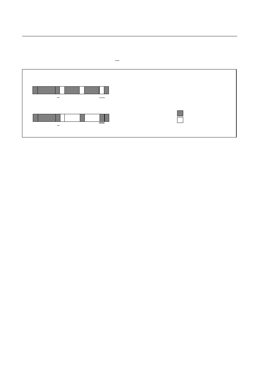
HYUNDAI
GMS81C4040/87C4060
May. 2000 Ver 1.0
67
Address data communication
The first transmitted data from master is compared with
I
2
C address register (ICAR, 00D8
H
). At this time R/W is
not compared but it determines next data operation. i.e,
transmitting or receiving data
Figure 18-11 Address data communication format
Master -> Slave (with 7bit address)
START
R/W
ACK
ACK
ACK
/ACK
Data
STOP
Slave addr.
Slave -> Master (with 7bit address)
Data block from master to slave
Data block from slave to master
7bit
Data
START
R/W
ACK
ACK
ACK
Data
STOP
Slave addr.
7bit
Data
("1")
("0")
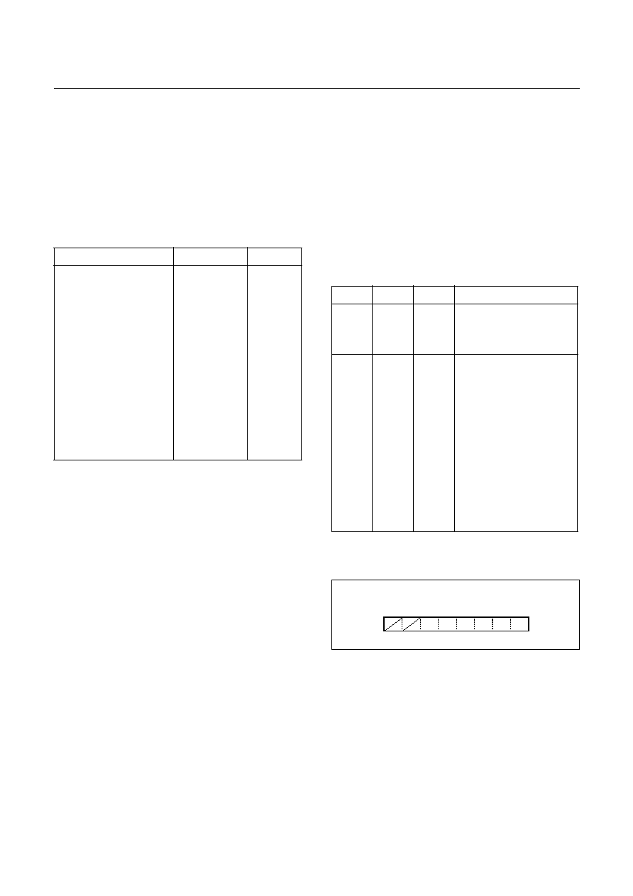
GMS81C4040/87C4060
HYUNDAI
68
May. 2000 Ver 1.0
19. INTERRUPTS
The GMS81C4040/GMS87C4060 interrupt circuits con-
sist of Interrupt enable register (IENH, IENL), Interrupt re-
quest flags of IRQH, IRQL, Priority circuit and Master
enable flag ("I" flag of PSW). 16 interrupt sources are pro-
vided. The configuration of interrupt circuit is shown in
Figure 19-2 .
Below table shows the Interrupt priority
The External Interrupts can each be transition-activated (1-
to-0 or 0-to-1 transition).
When an external interrupt is generated, the flag that gen-
erated it is cleared by the hardware when the service rou-
tine is vectored to only if the interrupt was transition-
activated.
T h e T i m e r /C o u nt e r I n te r r up t s a r e ge n e r a t e d b y
TnIF(n=0~3), which is set by a match in their respective
timer/counter register.
The Basic Interval Timer Interrupt is generated by BITIF
which are set by a overflow in the timer register.
The interrupts are controlled by the interrupt master enable
flag I-flag (bit 2 of PSW), the interrupt enable register
(IE NH, IE NL) a nd the interrupt reques t flags (in
IRQH,IRQL) except Power-on reset and software BRK in-
terrupt.
Interrupt Mode Register
It controls interrupt priority. It takes only one specified in-
terrupt.
Of course, interrupt's priority is fixed by H/W, but some-
times user want to get specified interrupt even if higher
priority interrupt was occured. Higher priority interrupt is
processed the next time.
It contains 2bit data to enable priority selection and 4bit
data to select specified interrupt.
Figure 19-1 Interrupt Mode Register
Reset/Interrupt
Symbol
Priority
Hardware Reset
External Interrupt 0
OSD Interrupt
External Interrupt 1
External Interrupt 2
Timer/Counter 0
Timer/Counter 2
1 Frame Interrupt
VSync Interrupt
Timer/Counter 1
Timer/Counter 3
Interrupt interval measure
Watchdog Timer
Basic Interval Timer
Serial I/O Interrupt
I
2
C Interrupt
RESET
INT0
OSD
INT1
INT2
Timer 0
Timer 2
1Frame
VSync
Timer 1
Timer 3
INTV(INT3/4)
WDT
BIT
SIO
I2C
-
1
2
3
4
5
6
7
8
9
10
11
12
13
14
15
Bit No.
Name
Value
Function
5,4
IM1~0
00
01
1X
Mode 0: H/W priority
Mode 1: S/W priority
Interrupt is disabled, even
if IE is set.
3~0
IP3~0
0000
0001
0010
0011
0100
0101
0110
0111
1000
1001
1010
1011
1100
1101
1110
1111
INT0
OSD
INT1
INT2
Timer 0
Timer 2
1Frame
VSync
Timer 1
Timer 3
INTV(INT3/4)
WDT
BIT
SIO
I2C
Not used
Table 19-1 Bit function
IMOD
ADDRESS : 00F3
H
RESET VALUE : Undefined
IM0
IP3
IP2
IP1
IP0
RW
RW
RW
RW
RW
RW
IM1
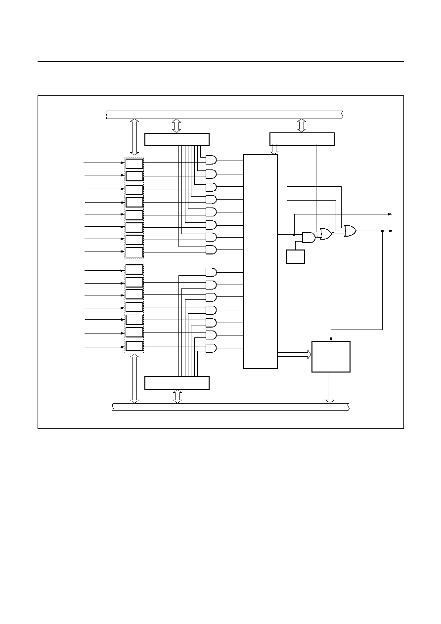
HYUNDAI
GMS81C4040/87C4060
May. 2000 Ver 1.0
69
Figure 19-2 Block Diagram of Interrupt
T0
Timer 0
INT2
INT1
INT2
INT1
IFOSD
OSD
INT0
INT0
IENH [00F6
H
]
Interrupt Enable
IRQH
Interrupt
Vector
Address
Generator
Internal bus line
Register (Higher byte)
To CPU
Interrupt Master
Enable Flag
I Flag
P
r
i
o
ri
t
y
Co
nt
rol
I-flag is in PSW , it is clea red by "D I", set b y
"EI" instruction. W hen it g oes interru pt service,
I-flag is cleared by hardw are , thus a ny othe r
in terrup t are inhibited. W hen in terrup t service is
com plete d by "R ETI" instru ction , I-fla g is se t to
"1" b y hardwa re.
T2
Timer 2
1Frame
1 Frame
VSync
IFVSync
WDT
IFWDT
IFBIT
IFS
BIT
SR
IFI2C
I2C
IENL [00F4
H
]
IRQL
INTV
Intr. interval
T3
Timer 3
T1
Timer 1
[00F5
H
]
Internal bus line
IMOD [00F3
H
]
Bit5
Interrupt Enable
Register (Lower byte)
RESET
BRK
[0F7
H
]
GMS81C4040/87C4060
HYUNDAI
70
May. 2000 Ver 1.0
Interrupt enable registers are shown in Figure 19-4 . These
registers are composed of interrupt enable flags of each in-
terrupt source, these flags determines whether an interrupt
will be accepted or not. When enable flag is "0", a corre-
sponding interrupt source is prohibited. Note that PSW
contains also a master enable bit, I-flag, which disables all
interrupts at once.
Figure 19-3 Interrupt Request Flags
INT2
R/W
INT0
VSync interrupt request flag
INITIAL VALUE: 0000 0000
b
ADDRESS: 00F7
H
IRQH
OSD
MSB
LSB
1Frame VSync
T0
T2
INT1
R/W
R/W
WDT
R/W
T1
INITIAL VALUE: 0000 000-
b
ADDRESS: 00F5
H
IRQL
T3
MSB
I2C
BIT
INTV
R/W
R/W
R/W
SR
R/W
R/W
R/W
R/W
R/W
R/W
R/W
R/W
1 Frame interrupt request flag
Timer / Counter 2 interrupt request flag
Timer / Counter 0 interrupt request flag
External interrupt 2 interrupt request flag
External interrupt 1 interrupt request flag
On screen display interrupt request flag
External interrupt 0 interrupt request flag
I
2
C interrupt request flag
LSB
Serial I/O interrupt request flag
Basic interval timer interrupt request flag
Watch-dog timer interrupt request flag
Interrupt interval measurement interrupt request flag (INT3/4)
Timer / Counter 3 interrupt request flag
Timer / Counter 1 interrupt request flag
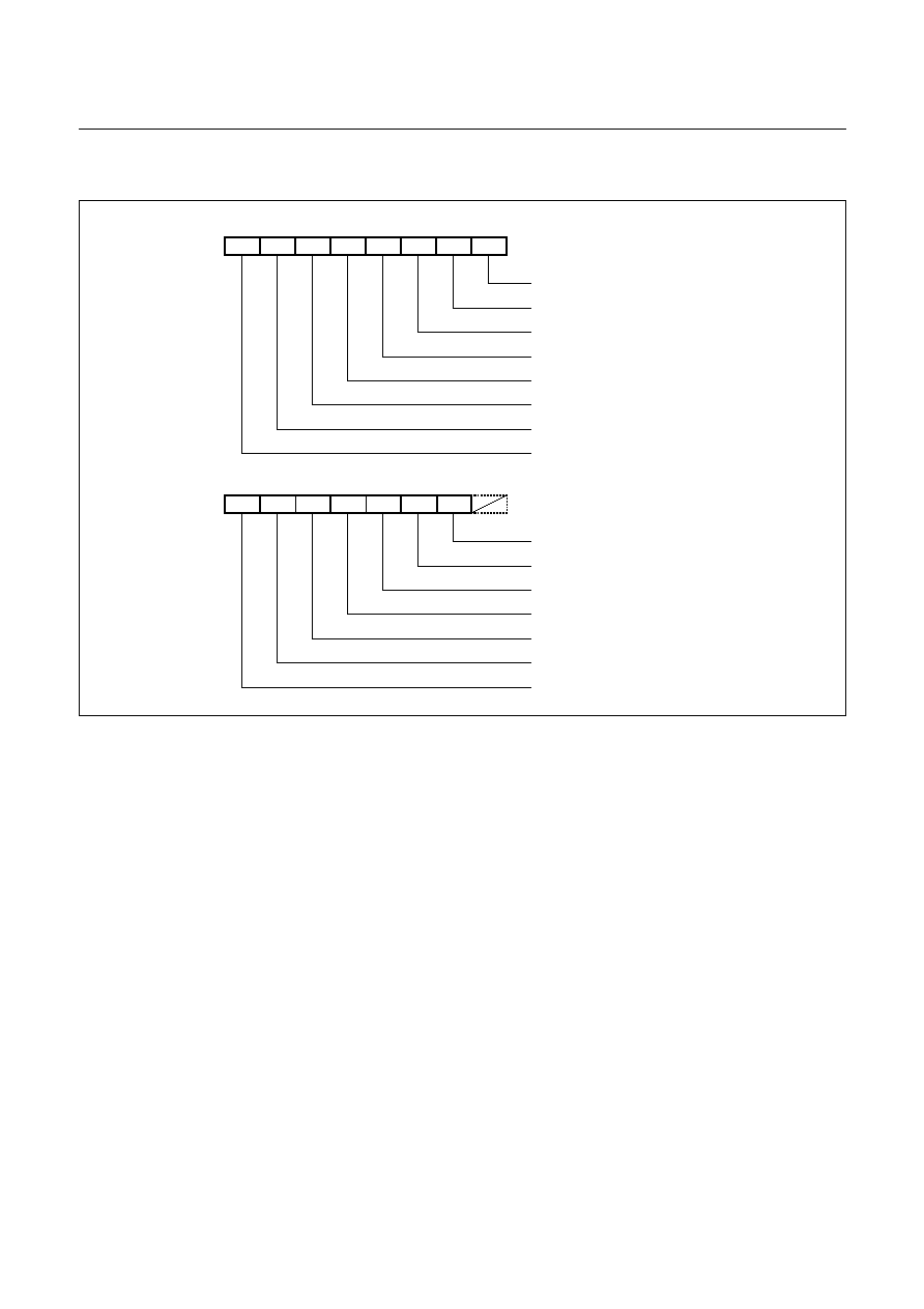
HYUNDAI
GMS81C4040/87C4060
May. 2000 Ver 1.0
71
Figure 19-4 Interrupt Enable Flags
INT2
R/W
INT0
VSync interrupt enable flag
INITIAL VALUE: 0000 0000
b
ADDRESS: 00F6
H
IENH
OSD
MSB
LSB
1Frame VSync
T0
T2
INT1
R/W
R/W
WDT
R/W
T1
INITIAL VALUE: 0000 000-
b
ADDRESS: 00F4
H
IENL
T3
MSB
I2C
BIT
INTV
R/W
R/W
R/W
SR
R/W
R/W
R/W
R/W
R/W
R/W
R/W
R/W
1Frame interrupt enable flag
Timer / Counter 2 interrupt enable flag
Timer / Counter 0 interrupt enable flag
External interrupt 2 interrupt enable flag
External interrupt 1 interrupt enable flag
On screen display interrupt enable flag
External interrupt 0 interrupt enable flag
I
2
C interrupt enable flag
LSB
Serial I/O interrupt enable flag
Basic interval timer interrupt enable flag
Watch-dog timer interrupt enable flag
Interrupt interval measurement interrupt enable flag (INT3/4)
Timer / Counter 3 interrupt enable flag
Timer / Counter 1 interrupt enable flag
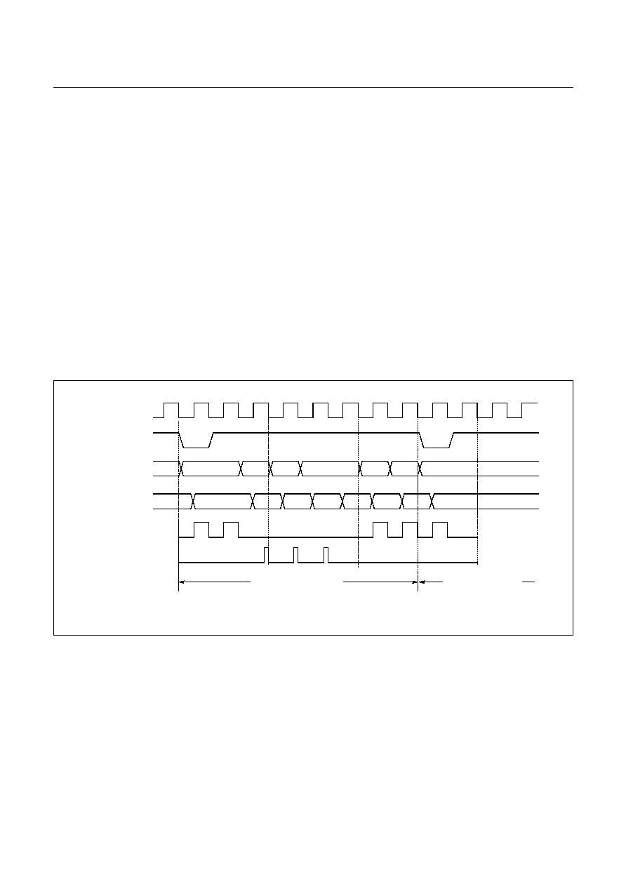
GMS81C4040/87C4060
HYUNDAI
72
May. 2000 Ver 1.0
19.1 Interrupt Sequence
An interrupt request is held until the interrupt is accepted
or the interrupt latch is cleared to "0" by a reset or an in-
struction. Interrupt acceptance sequence requires 8 f
ex
(2
�
s at f
MAIN
=4MHz) after the completion of the current in-
struction execution. The interrupt service task terminates
upon execution of an interrupt return instruction [RETI].
Interrupt acceptance
Figure 19-5 Interrupt Service routine Entering Timing
1. The interrupt master enable flag (I-flag) is cleared to
"0" to temporarily disable the acceptance of any fol-
lowing maskable interrupts. When a non-maskable in-
terrupt is accepted, the acceptance of any following
interrupts is temporarily disabled.
2. Interrupt request flag for the interrupt source accepted
is cleared to "0".
3. The contents of the program counter (return address)
and the program status word are saved (pushed) onto
the stack area. The stack pointer decrements 3 times.
4. The entry address of the interrupt service program is
read from the vector table address, and the entry ad-
dress is loaded to the program counter.
5. The instruction stored at the entry address of the inter-
rupt service program is executed.
V.L.
System clock
Address Bus
PC
SP
SP-1
SP-2
V.H.
New PC
V.L.
Data Bus
Not used
PCH
PCL
PSW
ADL
OP code
ADH
Instruction Fetch
Internal Read
Internal Write
Interrupt Processing Step
Interrupt Service Task
V.L. and V.H. are vector addresses.
ADL and ADH are start addresses of interrupt service routine as vector contents.
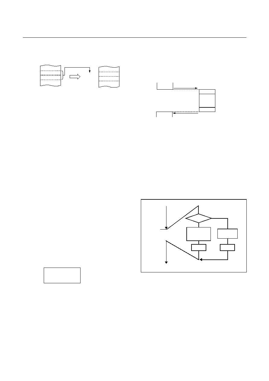
HYUNDAI
GMS81C4040/87C4060
May. 2000 Ver 1.0
73
A maskable interrupt is not accepted until the I-flag is set
to "1" even if a maskable interrupt of higher priority than
that of the current interrupt being serviced.
When nested interrupt service is necessary, the I-flag is set
to "1" in the interrupt service program. In this case, accept-
able interrupt sources are selectively enabled by the indi-
vidual interrupt enable flags.
Saving/Restoring General-purpose Register
During interrupt acceptance processing, the program
counter and the program status word are automatically
saved on the stack, but not the accumulator and other reg-
isters. These registers are saved by the program if neces-
sary. Also, when nesting multiple interrupt services, it is
necessary to avoid using the same data memory area for
saving registers.
The following method is used to save/restore the general-
purpose registers.
Example: Register save using push and pop instructions
General-purpose register save/restore using push and pop
instructions;
19.2 BRK Interrupt
Software interrupt can be invoked by BRK instruction,
which is the lowest priority order.
Interrupt vector address of BRK is shared with the vector
of TCALL 0 (Refer to Program Memory Section). When
BRK interrupt is generated, B-flag of PSW is set to distin-
guish BRK from TCALL 0.
Each processing step is determined by B-flag as shown in
Figure 19-6 .
Figure 19-6 Execution of BRK/TCALL0
INTxx:
PUSH
A
PUSH
X
LDA
DPGR
PUSH
A
;SAVE ACC.
;SAVE X REG.
;SAVE DPGR
; Direct page
; accessable reg.
;
:
interrupt processing
:
POP
A
STA
DPGR
POP
X
POP
A
RETI
;RESTORE DPGR
;RESTORE X REG.
;RESTORE ACC.
;RETURN
Basic Interval Timer
012
H
0E3
H
0FFE6
H
0FFE7
H
0E
H
2E
H
0E312
H
0E313
H
Entry Address
Correspondence between vector table address for BIT interrupt
and the entry address of the interrupt service program.
Vector Table Address
main task
interrupt
service task
saving
registers
restoring
registers
acceptance of
interrupt
interrupt return
B-FLAG
BRK
INTERRUPT
ROUTINE
RETI
TCALL0
ROUTINE
RET
BRK or
TCALL0
=0
=1
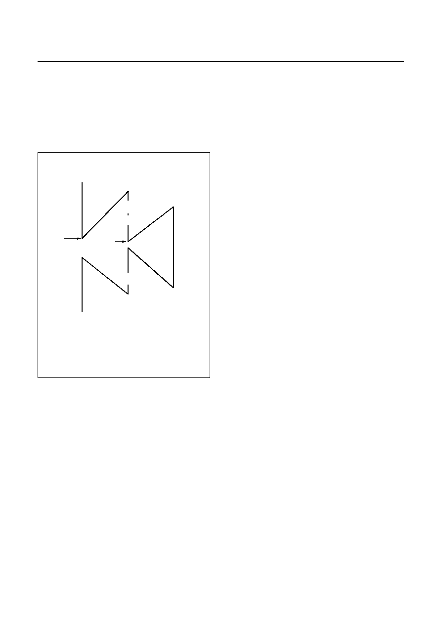
GMS81C4040/87C4060
HYUNDAI
74
May. 2000 Ver 1.0
19.3 Multi Interrupt
If two requests of different priority levels are received si-
multaneously, the request of higher priority level is ser-
viced. If requests of the same priority level are received
simultaneously, an internal polling sequence determines
by hardware which request is serviced.
Figure 19-7 Execution of Multi Interrupt
However, multiple processing through software for special
features is possible. Generally when an interrupt is accept-
ed, the I-flag is cleared to disable any further interrupt. But
as user set I-flag in interrupt routine, some further interrupt
can be serviced even if certain interrupt is in progress.
Example: Even though Timer1 interrupt is in progress,
INT0 interrupt serviced without any suspend.
TIMER1:
PUSH
A
PUSH
X
PUSH
Y
LDM
IENH,#80H
;
Enable INT0 only
LDM
IENL,#0
;
Disable other
EI
;
Enable Interrupt
:
:
:
:
:
:
LDM
IENH,#FFH
;
Enable all interrupts
LDM
IENL,#FEH
POP
Y
POP
X
POP
A
RETI
enable INT0
TIMER 1
service
INT0
service
Main Program
service
Occur
TIMER1 interrupt
Occur
INT0
EI
disable other
enable INT0
enable other
In this example, the INT0 interrupt can be serviced without any
pending, even TIMER1 is in progress.
Because of re-setting the interrupt enable registers IENH,IENL
and master enable "EI" in the TIMER1 routine.
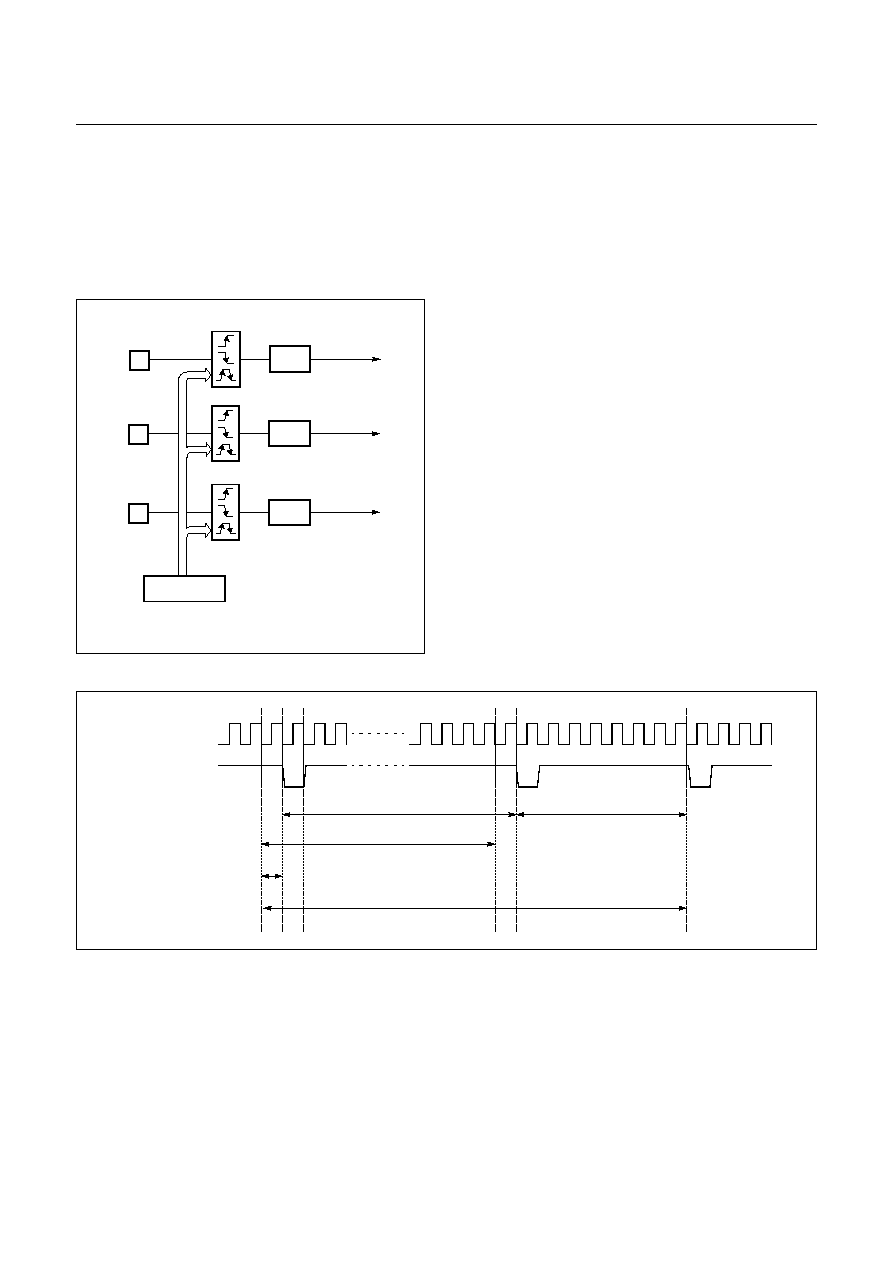
HYUNDAI
GMS81C4040/87C4060
May. 2000 Ver 1.0
75
19.4 External Interrupt
The external interrupt on INT0, INT1... pins are edge trig-
gered depending the edge selection register.
Refer to "6. PORT STRUCTURES" on page 9.
The edge detection of external interrupt has three transition
activated mode: rising edge, falling edge, both edge.
Figure 19-8 External Interrupt Block Diagram
INT0, INT1 and INT2 are multiplexed with general I/O
ports. To use external interrupt pin, the bit of port function
register FUNC1 should be set to "1" correspondingly.
Response Time
The INT0, INT1 and INT2 edge are latched into INT0IF,
INT1IF and INT2IF at every machine cycle. The values
are not actually polled by the circuitry until the next ma-
chine cycle. If a request is active and conditions are right
for it to be acknowledged, a hardware subroutine call to the
requested service routine will be the next instruction to be
executed. For example, the DIV instruction takes twelve
machine cycles. Thus, a minimum of twelve complete ma-
chine cycles elapse between activation of an external inter-
rupt request and the beginning of execution of the first
instruction of the service routine
Figure 19-9 Interrupt Response Timing Diagram ( Interrupt overhead )
INT0IF
INT0 pin
INT0 INTERRUPT
INT1IF
INT1 pin
INT1 INTERRUPT
INT2IF
INT2 pin
INT2 INTERRUPT
IEDS
[00F2
H
]
edge s
e
l
e
c
t
i
o
n
System clock
Instruction Fetch
Last instruction execution (0~12cycle)
Enter interrupt service routine (8cycle)
Interrupt request sampling
1cycle
Interrupt overhaed (9~21cycle)
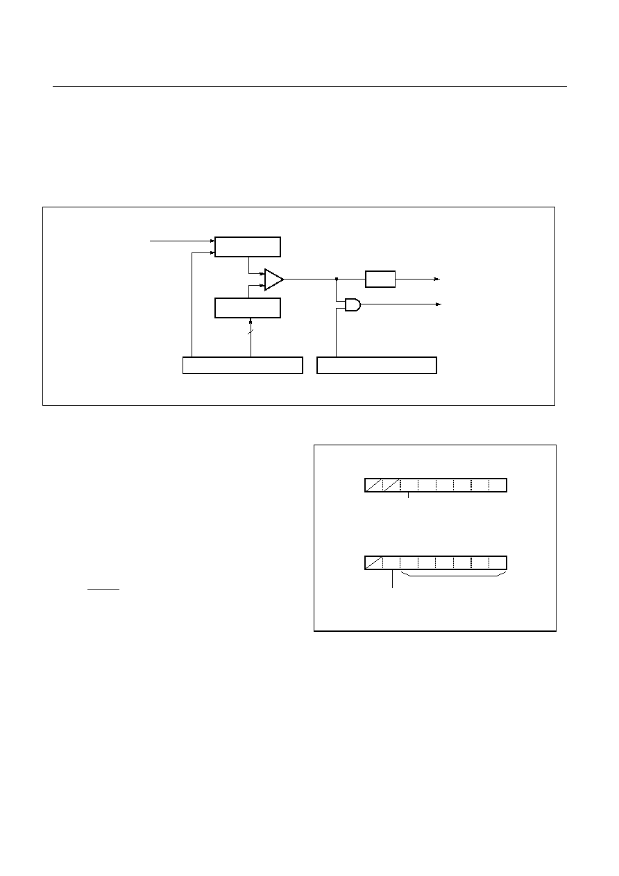
GMS81C4040/87C4060
HYUNDAI
76
May. 2000 Ver 1.0
20. WATCHDOG TIMER
The watchdog timer rapidly detects the CPU malfunction
such as endless looping caused by noise or the like, and re-
sumes the CPU to the normal state.
The watchdog timer signal for detecting malfunction can
be selected either a reset CPU or a interrupt request.
When the watchdog timer is not being used for malfunc-
tion detection, it can be used as a timer to generate an in-
terrupt at fixed intervals.
Figure 20-1 Block Diagram of Watchdog Timer
Watchdog Timer Control
Figure 20-2 shows the watchdog timer control register.
The watchdog timer is automatically disabled after reset.
The CPU malfunction is detected as setting the detection
time, selecting output, and clearing the binary counter. Re-
peatedly clearing the binary counter within the setting de-
tection time.
If the malfunction occurs for any cause, the watchdog tim-
er output will become active at the rising overflow from
the binary counters unless the binary counter are cleared.
At this time, when WDTON=1 a reset is generated, which
drives the RESET pin low to reset the internal hardware.
When WDTON=0, a watchdog timer interrupt (IFWDT) is
generated.
Figure 20-2 Watchdog timer register
to reset CPU
WDTR
Watchdog Timer Register
(BIT overflow : IFBIT)
Clock source
6-bit up-counter
enable
WDT
6-bit compare data
comparator
6
WDTR[bit5~0]
Watchdog Timer interrupt
WDTCL[bit6]
clear
[00D7
H
]
IFWDT
CKCTLR
Clock control Register
[00D6
H
]
WDTON[bit5]
CKTCLR
ADDRESS : 00D6
H
RESET VALUE : 0000 0000
b
WDT
ENP BTCL BTS2 BTS1 BTS0
Watchdog timer On/Off control
W
W
W
W
W
R
WDTR
ADDRESS : 00D7
H
RESET VALUE : -011 1111
b
WDT
W D T R 5 ~ 0
Slave address
W
W
W
W
W
W
W
ON
CK
0: Normal 6bit timer, Watchdog off
1: Watchdog timer
CL
Watchdog timer Clear
0: Watchdog timer free run
1: Watchdog timer clear and free run
Automatically cleared this bit after 1cycle
HYUNDAI
GMS81C4040/87C4060
May. 2000 Ver 1.0
77
Example: Sets the watchdog timer detection time
Enable and Disable Watchdog
Watchdog timer is enabled by setting WDTON (bit 5 in
CKTCLR) to "1". WDTON is initialized to "0" during re-
set, WDTON should be set to "1" to operate after reset is
released.
Example: Enables watchdog timer reset
:
LDM
CKTCLR,#001?????b ;WDTON
1
:
:
The watchdog timer is disabled by clearing bit 5 (WD-
TON) of CKTCLR.
Watchdog Timer Interrupt
The watchdog timer can also be used as a simple 6-bit tim-
er by clearing bit 5 (WDTON) of CKTCLR. The interval
of watchdog timer interrupt is decided by Basic Interval
Timer.
Interval equation is shown as below.
The stack pointer (SP) should be initialized before using
the watchdog timer output as an interrupt source.
Example: 6-bit timer interrupt setting up.
LDX
#03FH
TXSP
;SP
3F
LDM
CKTCLR,#000?????b ;WDTON
0
LDM
WDTR,#01??????b ;WDTCL
0
:
:
Refer table and see BIT timer ().
LDM
WDTR,#01??????b
;
Clear Counter and set value(??????b)
;
You have to set WDTR first, for prevent unpredictable interrupt
;
when you set WDTON bit.
LDM
CKCTLR,#00111???b
;
Select clock source(???b)
and WDTON=1
LDM
WDTR,#01??????b
;
Clear counter
:
:
:
:
LDM
WDTR,#01??????b
;
Clear counter
:
:
:
:
LDM
WDTR,#01??????b
;
Clear counter
Within WDT
detection time
Within WDT
detection time
�
�
�
�
=
CKCTLR
BTS2~0
BIT input
clock
Watchdog
timer input
clock
IFWDT cycle
000
b
PS4 (2uS)
512uS
32,256uS
001
b
PS5 (4uS)
1,024uS
64,512uS
010
b
PS6 (8uS)
2,048uS
129,024uS
011
b
PS7 (16uS)
4,096uS
258,048uS
100
b
PS8 (32uS)
8,192uS
516,096uS
101
b
PS9 (64uS)
16,384uS
1,032,192uS
110
b
PS10 (128uS)
32,768uS
2,064,384uS
111
b
PS11 (256uS)
65,536uS
4,128,768uS
Table 20-1 Watchdog timer MAX. cycle (Ex:f
ex
=8MHz)
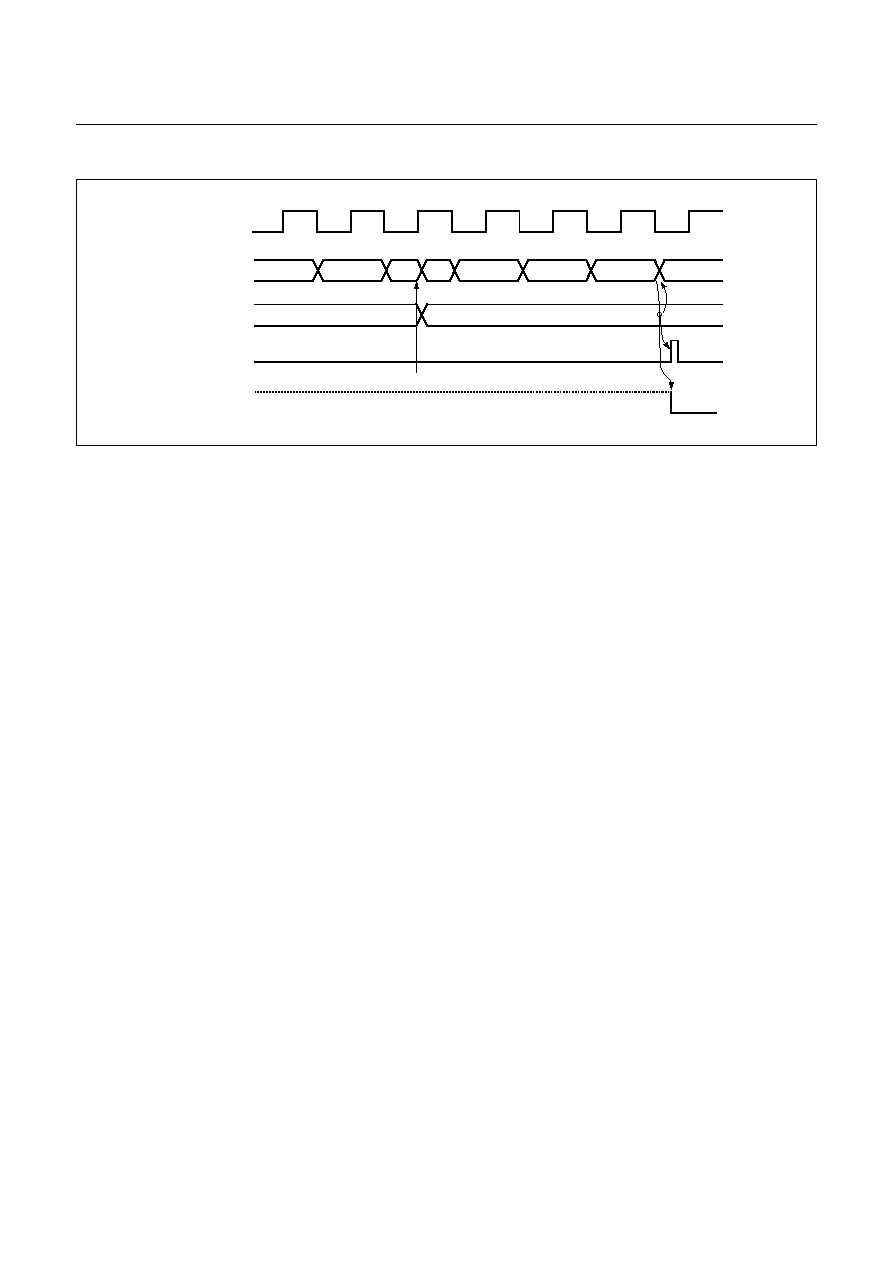
GMS81C4040/87C4060
HYUNDAI
78
May. 2000 Ver 1.0
Figure 20-3 Watchdog timer Timing
Minimizing Current Consumption
It should be set properly that current flow through port
doesn't exist.
First conseider the setting to input mode. Be sure that there
is no current flow after considering its relationship with
external circuit. In input mode, the pin impedance viewing
from external MCU is very high that the current doesn't
flow.
But input voltage level should be V
SS
or V
DD
. Be careful
that if unspecified voltage, i.e. if unfirmed voltage level is
applied to input pin, there can be little current (max. 1mA
at around 2V) flow.
If it is not appropriate to set as an input mode, then set to
output mode considering there is no current flow. Setting
to High or Low is decided considering its relationship with
external circuit. For example, if there is external pull-up re-
sistor then it is set to output mode, i.e. to High, and if there
is external pull-down register, it is set to low. See Figure
20-4 .
2
3
n
Source clock
Binary-counter
WDTR
IFWDT interrupt
WDTR
"0100_0011b"
1
0
Match
Detect
Counter
Clear
1
2
3
0
BIT overflow
3
WDT reset
reset
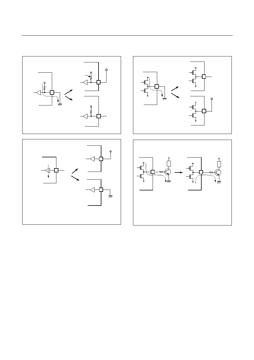
HYUNDAI
GMS81C4040/87C4060
May. 2000 Ver 1.0
79
Figure 20-4 Application example of Port under Power Consumption
INPUT PIN
V
DD
GND
i
V
DD
OUTPUT PIN
GND
i
X
Weak pull-up current flows
In the left case, much current flows from port to GND.
X
ON
OFF
V
DD
internal
pull-up
OUTPUT PIN
GND
i
In the left case, Tr. base current flows from port to GND.
i=0
X
OFF
ON
V
DD
L
ON
OFF
OPEN
GND
V
DD
L
ON
OFF
To avoid power consumption, low output to the port .
INPUT PIN
i
V
DD
X
Very weak current flows
V
DD
O
O
OPEN
ON
OFF
OPEN
i=0
O
O
V
DD
O
i=0
O
GND
O
When port is configured as an input, input level should
be closed to 0V or 5V to avoid power consumption.
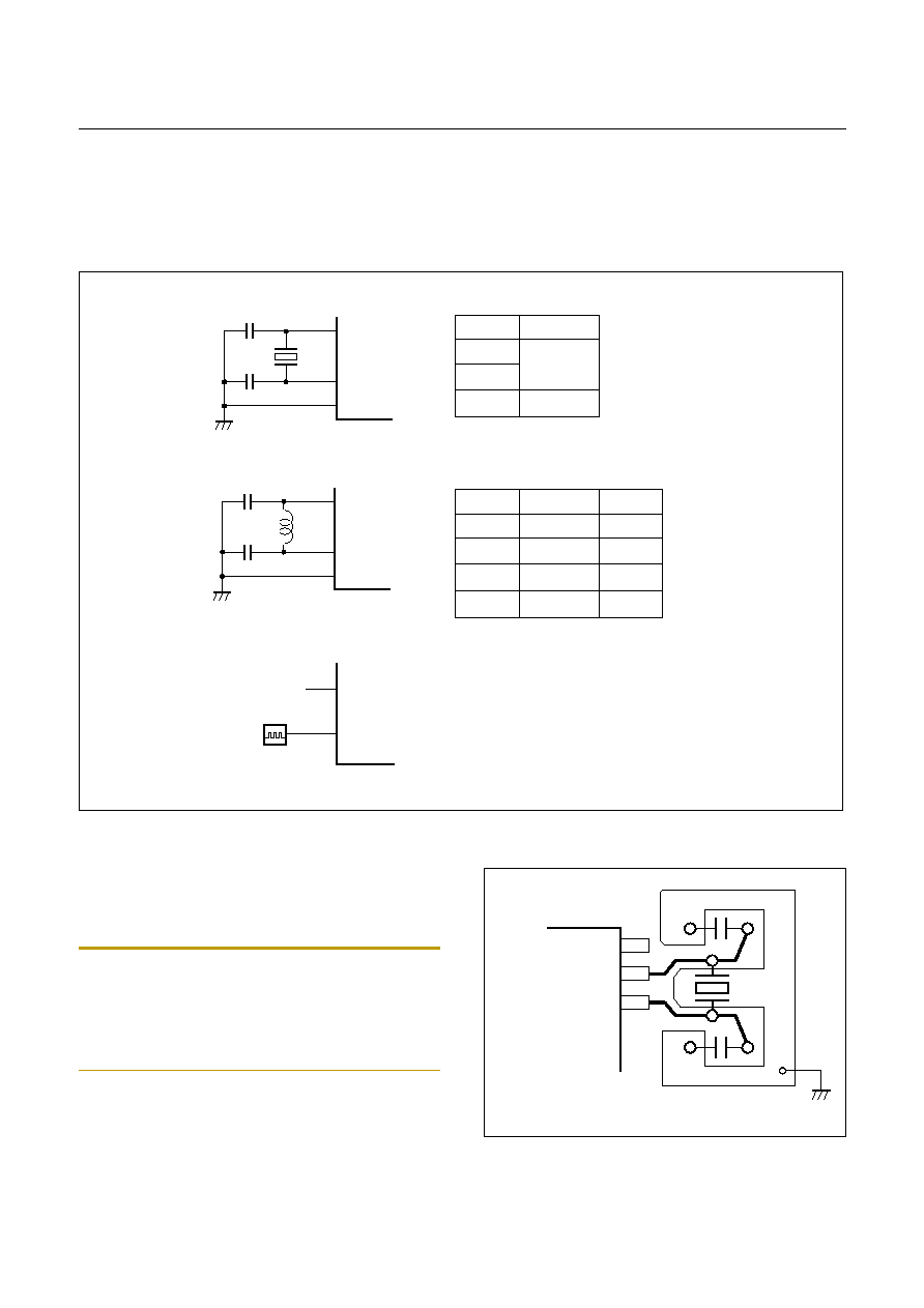
GMS81C4040/87C4060
HYUNDAI
80
May. 2000 Ver 1.0
21. OSCILLATOR CIRCUIT
The GMS81C4040/GMS87C4060 has two oscillation cir-
cuits internally. X
IN
and X
OUT
are input and output for
main frequency and OSC1 and OSC2 are input and output
for OSD(On Screen display) frequency, respectively, of a
inverting amplifier which can be configured for use as an
on-chip oscillator, as shown in Figure 21-1 .
Figure 21-1 Oscillation Circuit
Oscillation components have their own characteristics, so
user should consult the component manufacturers for ap-
propriate values of external components.
In addition, see Figure 21-2 for the layout of the crystal.
Note: Minimize the wiring length. Do not allow wiring to in-
tersect with other signal conductors. Do not allow wiring to
come near changing high current. Set the potential of the
grounding position of the oscillator capacitor to that of V
SS
.
Do not ground to any ground pattern where high current is
present. Do not fetch signals from the oscillator.
Figure 21-2 Layout example of Oscillator PCB circuit
X
OUT
X
IN
V
SS
Recommend
C1
C2
X
OUT
X
IN
External Clock
Open
External Oscillator
LC Oscillator
Crystal Oscillator
fc (MHz)
you have to tune the
For selection L,C value,
OSC2
OSC1
V
SS
frequency to appropriate
range which is dependent
to your target set.
C1
C2
L1
fc (MHz)
10
12
16
C1 & C2 (pF)
30
5
Recommend
fc (MHz)
8
12
16
C1 & C2 (pF)
L (uH)
20
5
20
10
5
100
15
15
15
X
OUT
X
IN
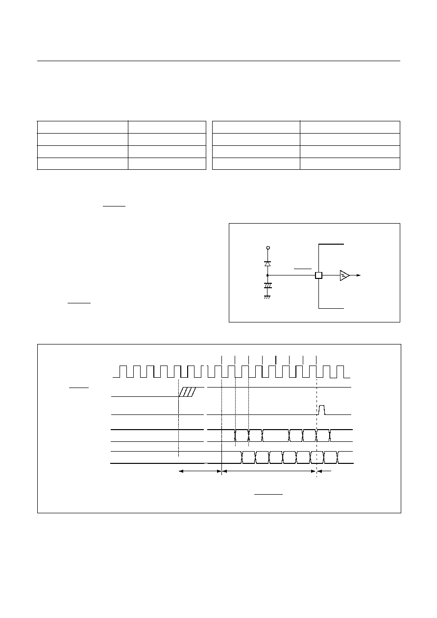
HYUNDAI
GMS81C4040/87C4060
May. 2000 Ver 1.0
81
22. RESET
The GMS81C4040/GMS87C4060 have two types of reset
generation procedures; one is an external reset input, other
is a watch-dog timer reset. Table 22-1 shows on-chip hard-
ware initialization by reset action.
Table 22-1 Initializing Internal Status by Reset Action
22.1 External Reset Input
The reset input is the RESET pin, which is the input to a
Schmitt Trigger. A reset in accomplished by holding the
RESET pin low for at least 8 oscillator periods, within the
operating voltage range and oscillation stable, a reset is ap-
plied and the internal state is initialized. After reset, 64ms
(at 4 MHz) add with 7 oscillator periods are required to
start execution as shown in Figure 22-2 .
Internal RAM is not affected by reset. When V
DD
is turned
on, the RAM content is indeterminate. Therefore, this
RAM should be initialized before reading or testing it.
When the RESET pin input goes high, the reset operation
is released and the program execution starts at the vector
address stored at addresses FFFE
H
- FFFF
H
.
A connecting for simple power-on-reset is shown in Figure
22-1 .
Figure 22-1 Simple Power-on-Reset Circuit
Figure 22-2 Timing Diagram after RESET
On-chip Hardware
Initial Value
On-chip Hardware
Initial Value
Program counter
PC
(FFFF
H
) - (FFFE
H
)
Peripheral clock
Off
RAM page register
DPGR
00
H
Watchdog timer
Disable
G-flag of PSW
G
0
Control registers
Refer to Table 8-1 on page 22
RESET
+
-
V
DD
GND
MCU
MAIN PROGRAM
Oscillator
(X
IN
pin)
?
?
FFFE FFFF
Stabilization Time
t
ST
= 62.5mS at 4.19MHz
RESET
ADDRESS
DATA
1
2
3
4
5
6
7
?
?
Start
?
?
?
FE
?
ADL
ADH
OP
BUS
BUS
RESET Process Step
~~
~~
~~
~~
~~
~~
t
ST
=
x 256
f
MAIN
�
1024
1
Fetch
~~

GMS81C4040/87C4060
HYUNDAI
82
May. 2000 Ver 1.0
22.2 Watchdog Timer Reset
Refer to "20. WATCHDOG TIMER" on page 76.

HYUNDAI
GMS81C4040/87C4060
May. 2000 Ver 1.0
83
23. OTP Programming
23.1 GMS87C4060 OTP Programming
You can burn out GMS87C4060 OTP through the general
Gang programmer using Intel 27010/C010 mode. In Dev-
leopment tool package auxiliary, GMS87C4060-to-27010/
C010 conversion socket is included. GMS87C4060 have
two ROM memory areas. One is Program ROM memory
and the other is Font ROM memory. Program ROM area is
from 1000h to FFFFh Font ROM area is from 10000h to
13FFFh. When you acquire new OTP, actually, the OTP is
not fully blank. The OPT have six test pattern in the OSD
Font ROM memory(see figure23-1). The test pattern are
written at 11FA0h ~ 11FFFh and 13FA0h ~ 13FFFh.
Note: DO NOT write any data in this area(11FA0h ~
11FFFh, 13FA0h ~ 13FFFh)
Blank Check
If you run blank check function of ROM writer, ROM
writer inform blank error because of test pattern. To avoid
this situation, you must run the blank check function sep-
eretely. For example, check OTP address rage of 1000h ~
11F9Fh at first. And then check OPT address range of
12000h ~ 13F9Fh. If you have ROM writer without partial
blank check function, please do not run blank check func-
tion.
Figure 23-1 GMS87C4060 OTP Memory Map
Program Writing
There are two kind of OTP file. One is program OTP
file(***.OTP) and the other is font OTP file(***.FNT).
You can make each file through ASMLINKER.exe and
OSDFONT.exe respectively. All OTP file is Motolora S-
format. You can burn the program file and font file respec-
tively or together. To burn program file and font file re-
spectively, refer following procedure
1. Make program OTP file and font OTP file repec-
tively.
2. Check whether six test pattern is included in font
OTP file(see below Six Text Pattern)
3. Burn program OTP file(Set chip target address
1000h ~ FFFFh)
4. Burn font OTP file(Set chip target address 10000h
~13FFFh)
Note: When you program the OTP file, DO NOT check the
blank. Because there are already written data(Six test pat-
tern / 11FA0h ~ 11FFFh, 13FA0h~13FFFh) It will occur
blank error
To burn program file and font file together, refer following
procedure
1. Add program OTP file and font OTP file
2. Check whether six test pattern is included in font
OTP file(see below Six Text Pattern)
3. Burn OTP file(Set chip target address 1000h ~
13FFFh)
About other details, refer ROM wirter manual.
Six Test Pattern
When you make font file through OSDFONT.exe, please
confirm whether six test pattern is included or not in char-
acter address 1FAh ~ 1FFh, To include six test patern, refer
following procedure.
1. Make Font file and save it to your PC
2. Reopen the font file and save it to your HDD once
again.
3. Then six test pattern will be included automatically.
(Character address 1FAh ~ 1FFh)
1000H
FFFFH
13FFFH
OSD Font
Memory
Program
Memory
GMS81C4040/87C4060
HYUNDAI
84
May. 2000 Ver 1.0
23.2 .Device configuration data
Figure 23-2 Figure Pin Configuration in OTP Programming Mode
Figure 23-3 Figure Mode Table
HY
UNDAI
GMS8
74
060
A15
A14
A13
A12
A11
A10
A9
A8
A7
A6
A3
A2
A1
A0
O7
O6
O5
O4
O3
A16
A4
A5
GND
CEB
PGMB
OEB
V
CC
V
PP
O0
O1
O2
1
2
3
4
5
6
7
8
9
10
11
12
13
14
15
16
17
18
19
20
21
22
23
24
25
26
52
51
50
49
48
47
46
45
44
43
42
41
40
39
38
37
36
35
34
33
32
31
30
29
28
27
GMS87C4060
Intel 27010
Mode
VPP
CEB
OEB
PGMB
VPP
CEB
OEB
PGMB
Program
12.75V
Low
High
*2
Low
*1
12.75V
Low
High
Low
Verify
12.75V
Low
Low
High
12.75V
Low
Low
High
Optional
Verify
5V
Low
Low
X
5V
Low
Low
X
Gang
Write
*3
12.75V
Low
High
Low
12.75V
Low
High
Low
Gang
Verify
*4
12.75V,
5V
Low
Low
X
12.75V
Low
Low
X
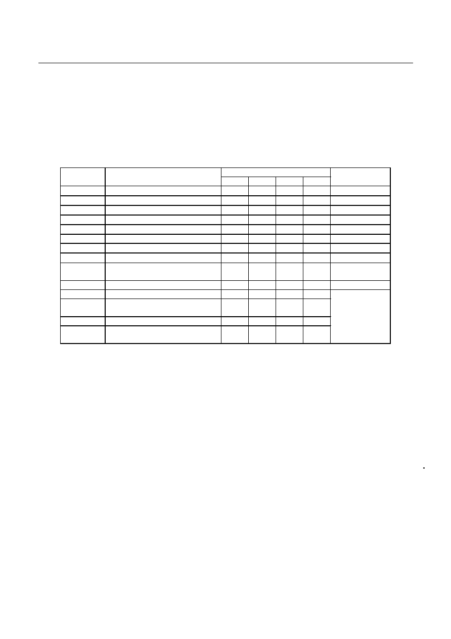
HYUNDAI
GMS81C4040/87C4060
May. 2000 Ver 1.0
85
*1: Low = Input Low Voltage = V
IL
(<0.8V)
*2: High = Input High Value = VIL(>2.0V)
*3: In Gang Write Mode, All OTPs are programmed sim-
ulaneously. So all signals of OTPs are in the same condi-
tion
*4: In Gang Verify mode, the VPP pin can be sset to both
normal high(5V), aand 12.75V and chip slecection is pos-
sible using the CEB pin
Figure 23-4 Figure AC Programming Characteristics
Limits
SYMBOL
Parameter
Min
Typ
Max
Unit
Conditions
tAS
Address Setup Time
2
�
s
tOES
OEB Setup Time
2
�
s
tDS
Data Setup Time
2
�
s
tAH
Address Hold Time
0
�
s
tDH
Data Hold Time
2
�
s
tDFP
OEB High to Output Float Delay
0
130
ns
Note1
tVPS
Vpp Setup Time
2
�
s
tCES
CEB Setup Time
2
�
s
tPW
PGMB initial program pulse width
95
100
105
�
s
Quick pulse
programming
tOE
Data Valid from OEB
100
ns
tACC
Address to output delay
150
ns
tOH
output hold from addresses CEB or
OEB whichever occurrs first
0
0
ns
tCE
CEB to output delay
100
ns
tCS
chip selection interval
(@Gang verify)
100
ns
*Note1: Output Float is defined as the point where data is no longer driven

GMS81C4040/87C4060
HYUNDAI
86
May. 2000 Ver 1.0
Figure 23-5 Pin Mapping Table between Intel 27010/C010 and GMS87C4060
Intel 27010
GMS87C4060
Pin Name
Pin Number
Pin Name
Pin Number
VPP
1
TEST_N
38
A16
2
R67
26
A15
3
R27
1
A12
4
R24
4
A7
5
R17
9
A6
6
R16
10
A5
7
R15
15
A4
8
R14
16
A3
9
R13
17
A2
10
R12
18
A1
11
R11
19
A0
12
R10
20
O0
13
R00
29
O1
14
R01
28
O2
15
R02
27
GND
16
VSS
12, 40
O3
17
R03
25
O4
18
R04
24
O5
19
R05
23
O6
20
R06
22
O7
21
R07
21
CEB
22
R41
51
A10
23
R22
6
OEB
24
R53
41
A11
25
R23
5
A9
26
R21
7
A8
27
R20
8
A13
28
R25
3
A14
29
R26
2
N.C.
30
PGMB
31
R52
42
VCC
32
VDD
39
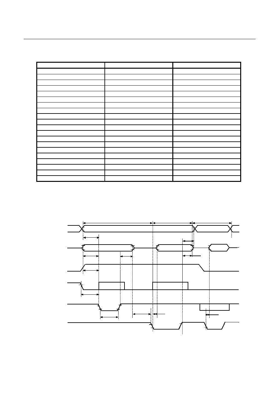
HYUNDAI
GMS81C4040/87C4060
May. 2000 Ver 1.0
87
Figure 23-6 Connection of Other Pins of GMS87C4060 in OTP Mode
23.3 Timing Chart
Figure 23-7 Figure Programming Timing Chart
Pin Name
Pin Number
Connect to
RESET_N
11
GND
Xout
13
Not Connect
Xin
14
GND
R
30
Not Connect
G
31
Not Connect
B
32
Not Connect
R56
33
Not Connect
R55
34
Not Connect
R54
35
Not Connect
OSC2
36
Not Connect
OSC1
37
GND
R47
45
GND
R46
46
GND
R45
47
GND
R44
48
GND
R43
49
Not Connect
R42
50
Not Connect
R40
52
GND
R50
44
VDD
R51
43
VDD
Address
VPP
Data in Stable
CEB
Data
PGMB
OEB
V
IH
V
IL
V
IH
V
IL
12.5V
5V
V
IH
V
IL
Data out Valid
Valid ouput
V
IH
V
IL
V
IH
V
IL
Address Stable
Program
Verify
Optinal Verify
Address Valid
tAS
tDS
tDH
tVPS
tAH
tDFP
tCES
tPW
tOES
tOE
tOE
High Z
Don't care
Don't care
Don't care
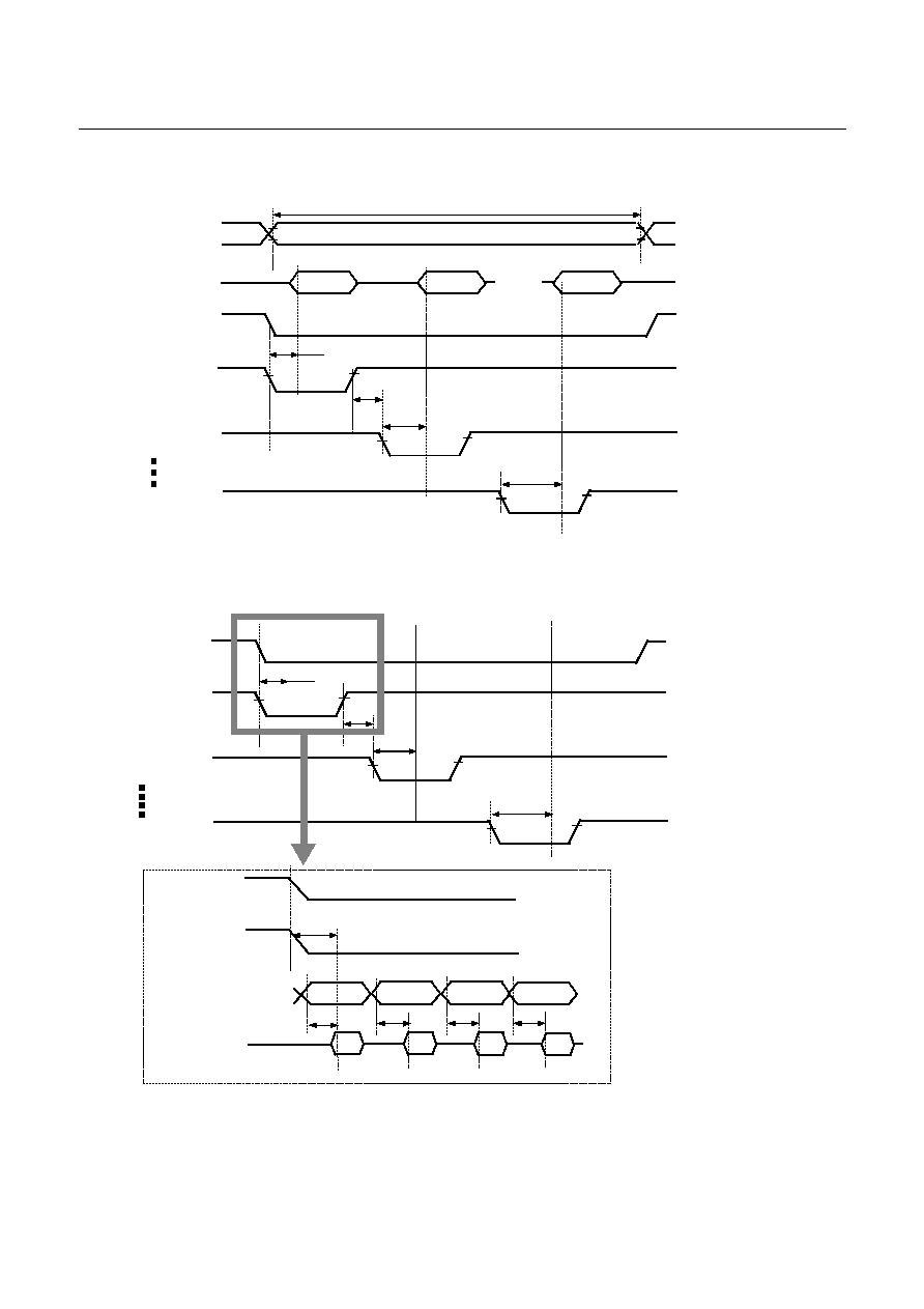
GMS81C4040/87C4060
HYUNDAI
88
May. 2000 Ver 1.0
Figure 23-8 AC Wave Form in Gang Verify Mode
Address
OEB
Data
CEB[0]
V
IH
V
IL
V
IH
V
IL
V
IH
V
IL
V
IH
V
IL
Address Stable
Optinal Verify
0th OTP
1st OTP
Data
Data
Data
.....
tACC
(n-1)th OTP
CEB[1]
V
IH
V
IL
tCS
tACC
CEB[n-1]
V
IH
V
IL
tACC
1) When you verify the data in the same address of many OTPs.
When you select OTPs using CEB, and can verify the data inthe same address.
(PGMB : Don't care , Vpp : V
IH
or 12.5V )
OEB
CEB[0]
V
IH
V
IL
V
IH
V
IL
tACC
CEB[1]
V
IH
V
IL
tCS
tACC
CEB[n-1]
V
IH
V
IL
tACC
OEB
CEB[0]
V
IH
V
IL
V
IH
V
IL
tACC
Addr0
Addr2
Addr3
Addr1
Data0
Data1
Data2
Data3
tACC
tACC
tACC
tACC
Data
Address
V
IH
V
IL
V
IH
V
IL
2) When you verify the data in s single OTP throughout the ROM address
HYUNDAI
GMS81C4040/87C4060
May. 2000 Ver 1.0
89
24. Assemble mnemonics
24.1 Instruction Map
00000
00
00001
01
00010
02
00011
03
00100
04
00101
05
00110
06
00111
07
01000
08
01001
09
01010
0A
01011
0B
01100
0C
01101
0D
01110
0E
01111
0F
000
NOP
SET1
dp.bit
BBS
A.bit,rel
BBS
dp.bit,rel
ADC
#imm
ADC
dp
ADC
dp+X
ADC
!abs
ASL
A
ASL
dp
TCALL
0
SETA1
.bit
BIT
dp
POP
A
PUSH
A
BRK
001
CLRC
//
//
//
SBC
#imm
SBC
dp
SBC
dp+X
SBC
!abs
ROL
A
ROL
dp
TCALL
2
CLRA1
.bit
COM
dp
POP
X
PUSH
X
BRA
rel
010
CLRG
//
//
//
CMP
#imm
CMP
dp
CMP
dp+X
CMP
!abs
LSR
A
LSR
dp
TCALL
4
NOT1
M.bit
TST
dp
POP
Y
PUSH
Y
PCALL
Upage
011
DI
//
//
//
OR
#imm
OR
dp
OR
dp+X
OR
!abs
ROR
A
ROR
dp
TCALL
6
OR1
OR1B
CMPX
dp
POP
PSW
PUSH
PSW
RET
100
CLRV
//
//
//
AND
#imm
AND
dp
AND
dp+X
AND
!abs
INC
A
INC
dp
TCALL
8
AND1
AND1B
CMPY
dp
CBNE
dp+X
TXSP
INC
X
101
SETC
//
//
//
EOR
#imm
EOR
dp
EOR
dp+X
EOR
!abs
DEC
A
DEC
dp
TCALL
10
EOR1
EOR1B
DBNE
dp
XMA
dp+X
TSPX
DEC
X
110
SETG
//
//
//
LDA
#imm
LDA
dp
LDA
dp+X
LDA
!abs
TXA
LDY
dp
TCALL
12
LDC
LDCB
LDX
dp
LDX
dp+Y
XCN
DAS
111
EI
//
//
//
LDM
dp,#imm
STA
dp
STA
dp+X
STA
!abs
TAX
STY
dp
TCALL
14
STC
M.bit
STX
dp
STX
dp+Y
XAS
10000
10
10001
11
10010
12
10011
13
10100
14
10101
15
10110
16
10111
17
11000
18
11001
19
11010
1A
11011
1B
11100
1C
11101
1D
11110
1E
11111
1F
000
BPL
rel
CLR1
dp.bit
BBC
A.bit,rel
BBC
dp.bit,rel
ADC
{X}
ADC
!abs+Y
ADC
[dp+X]
ADC
[dp]+Y
ASL
!abs
ASL
dp+X
TCALL
1
JMP
!abs
BIT
!abs
ADDW
dp
LDX
#imm
JMP
[!abs]
001
BVC
rel
//
//
//
SBC
{X}
SBC
!abs+Y
SBC
[dp+X]
SBC
[dp]+Y
ROL
!abs
ROL
dp+X
TCALL
3
CALL
!abs
TEST
!abs
SUBW
dp
LDY
#imm
JMP
[dp]
010
BCC
rel
//
//
//
CMP
{X}
CMP
!abs+Y
CMP
[dp+X]
CMP
[dp]+Y
LSR
!abs
LSR
dp+X
TCALL
5
MUL
TCLR1
!abs
CMPW
dp
CMPX
#imm
CALL
[dp]
011
BNE
rel
//
//
//
OR
{X}
OR
!abs+Y
OR
[dp+X]
OR
[dp]+Y
ROR
!abs
ROR
dp+X
TCALL
7
DBNE
Y
CMPX
!abs
LDYA
dp
CMPY
#imm
RETI
100
BMI
rel
//
//
//
AND
{X}
AND
!abs+Y
AND
[dp+X]
AND
[dp]+Y
INC
!abs
INC
dp+X
TCALL
9
DIV
CMPY
!abs
INCW
dp
INC
Y
TAY
101
BVS
rel
//
//
//
EOR
{X}
EOR
!abs+Y
EOR
[dp+X]
EOR
[dp]+Y
DEC
!abs
DEC
dp+X
TCALL
11
XMA
{X}
XMA
dp
DECW
dp
DEC
Y
TYA
110
BCS
rel
//
//
//
LDA
{X}
LDA
!abs+Y
LDA
[dp+X]
LDA
[dp]+Y
LDY
!abs
LDY
dp+X
TCALL
13
LDA
{X}+
LDX
!abs
STYA
dp
XAY
DAA
111
BEQ
rel
//
//
//
STA
{X}
STA
!abs+Y
STA
[dp+X]
STA
[dp]+Y
STY
!abs
STY
dp+X
TCALL
15
STA
{X}+
STX
!abs
CBNE
dp
XYX
NOP
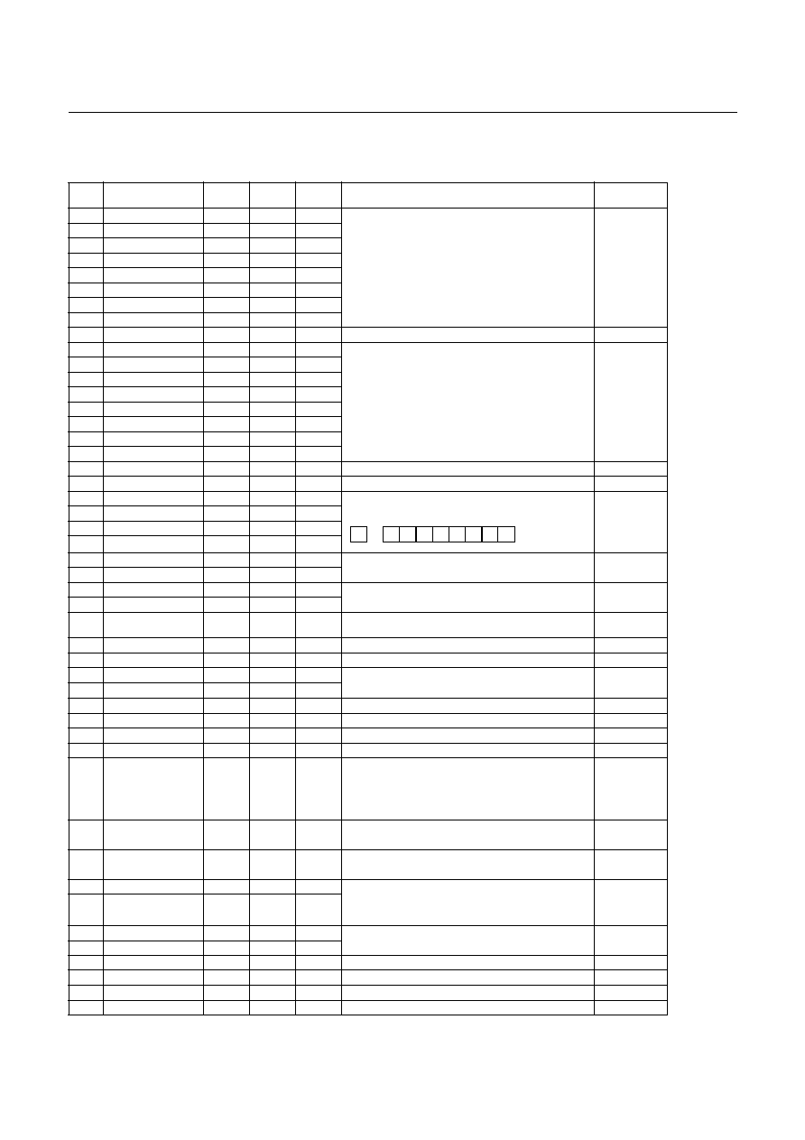
GMS81C4040/87C4060
HYUNDAI
90
May. 2000 Ver 1.0
24.2 Alphabetic order table of instruction
NO.
MNENONIC
OP
CODE
BYTE
NO.
CYCLE
NO
OPERATION
FLAG
NVGBHIZC
1
ADC #imm
04
2
2
Add with carry.
NV - - H - ZC
2
ADC dp
05
2
3
A
A + (M) + C
3
ADC dp + X
06
2
4
4
ADC !abs
07
3
4
5
ADC !abs+Y
15
3
5
6
ADC [dp+X]
16
2
6
7
ADC [dp]+Y
17
2
6
8
ADC {X}
14
1
3
9
ADDW dp
1D
2
5
16-bits add without carry : YA
YA + (dp+1)(dp)
NV - - H - ZC
10
AND #imm
84
2
2
Logical AND
N - - - - - Z -
11
AND dp
85
2
3
A
A ^ (M)
12
AND dp + X
86
2
4
13
AND !abs
87
3
4
14
AND !abs+Y
95
3
5
15
AND [dp+X]
96
2
6
16
AND [dp] + Y
97
2
6
17
AND {X}
94
1
3
18
AND1 M.bit
8B
3
4
Bit AND C-flag : C
C ^ (M.bit)
- - - - - - - C
19
AND1B M.bit
8B
3
4
Bit AND C-flag and NOT : C
C ^ ~(M.bit)
- - - - - - - C
20
ASL A
08
1
2
Arithmetic shift left
N - - - - - ZC
21
ASL dp
09
2
4
22
ASL dp + X
19
2
5
23
ASL !abs
18
3
5
24
BBC A.bit,rel
y2
2
4/6
Branch if bit clear :
- - - - - - - -
25
BBC dp.bit,rel
y3
3
5/7
if(bit) = 0, then PC
PC + rel
26
BBS A.bit,rel
x2
2
4/6
Branch if bit clear :
- - - - - - - -
27
BBS dp.bit,rel
x3
3
5/7
if(bit) = 1, then PC
PC + rel
28
BCC rel
50
2
2/4
Branch if carry bit clear :
if(C) = 0, then PC
PC + rel
MM - - - - Z -
29
BCS rel
D0
2
2/4
Branch if carry bit set : If (C) =1, then PC
PC + rel
- - - - - - - -
30
BEQ rel
F0
2
2/4
Branch if equal : if (Z) = 1, then PC
PC + rel
- - - - - - - -
31
BIT dp
0C
2
4
Bit test A with memory :
MM - - - - Z -
32
BIT !abs
1C
3
5
Z
A ^ M, N
(M
7
), V
(M
6
)
33
BMI rel
90
2
2/4
Branch if munus : if (N) = 1, then PC
PC + rel
- - - - - - - -
34
BNE rel
70
2
2/4
Branch if not equal : if (Z) = 0, then PC
PC + rel
- - - - - - - -
35
BPL rel
10
2
2/4
Branch if not minus : if (N) = 0, then PC
PC + rel
- - - - - - - -
36
BRA rel
2F
2
4
Branch always : PC
PC + rel
- - - - - - - -
37
BRK
0F
1
8
Software interrupt:
- - - 1 - 0 - -
B
"1", M(SP)
(PC
H
), SP
SP - 1,
M(s)
(PC
L
), SP
S - 1, M(SP)
PSW,
SP
SP - 1, PC
L
(0FFDE
H
), PC
H
(0FFDF
H
)
38
BVC rel
30
2
2/4
Branch if overflow bit clear :
- - - - - - - -
If (V) = 0, then PC
PC + rel
39
BVS rel
B0
2
2/4
Branch if overflow bit set :
- - - - - - - -
If (V) = 1, then PC
PC + rel
40
CALL !abs
3B
3
8
Subroutine call
- - - - - - - -
41
CALL [dp]
5F
2
8
M(SP)
(PC
H
), SP
SP-1, M(SP)
(PC
L
), SP
SP-1
if !abs, PC
abs ; if [dp], PC
L
(dp), PC
H
(dp+1)
42
CBNE dp,rel
FD
3
5/7
Compare and branch if not equal ;
- - - - - - - -
43
CBNE dp + X, rel
8D
3
6/8
If A
(M), then PC
PC + rel.
44
CLR1 dp.bit
y1
2
4
Clear bit : (M.bit)
"0"
- - - - - - - -
45
CLR1A A.bit
2B
2
2
Clear A.bit : (A.bit)
"0"
- - - - - - - -
46
CLRC
20
1
2
Clear C-flag : C
"0"
- - - - - - - 0
47
CLRG
40
1
2
Clear G-flag : G
"0"
- - 0 - - - - -
C 7 6 5 4 3 2 1 0
"
0
"
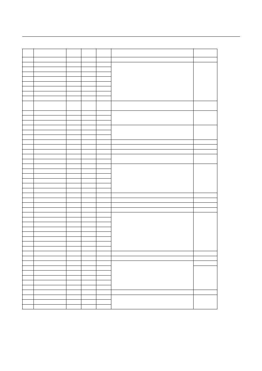
HYUNDAI
GMS81C4040/87C4060
May. 2000 Ver 1.0
91
48
CLRV
80
1
2
Clear V-flag : V
"0"
- 0 - - 0 - - -
49
CMP #imm
44
2
2
Compare accumulator contents with memory contents
N - - - - - ZC
50
CMP dp
45
2
3
A - (M)
51
CMP dp + X
46
2
4
52
CMP !abs
47
3
4
53
CMP !abs + Y
55
3
5
54
CMP [dp + X]
56
2
6
55
CMP [dp] + Y
57
2
6
56
CMP {X}
54
1
3
57
CMPW dp
5D
2
4
Compare YA contents with memory pair contents :
N - - - - - ZC
YA - (dp+1)(dp)
58
CMPX #imm
5E
2
2
Compare X contents with memory contents
N - - - - - ZC
59
CMPX dp
6C
2
3
X - (M)
60
CMPX !abs
7C
3
4
61
CMPY #imm
7E
2
2
Compare Y contents with memory contents
N - - - - - ZC
62
CMPY dp
8C
2
3
Y - (M)
63
CMPY !abs
9C
3
4
64
COM dp
2C
2
4
1's complement : (dp)
~(dp)
N - - - - - Z -
65
DAA
DF
1
3
Decimal adjust for addition
N - - - - - ZC
66
DAS
CF
1
3
Decimal adjust for substraction
N - - - - - ZC
67
DBNE dp,rel
AC
3
5/7
Decrement and branch if not equal :
- - - - - - - -
68
DBNE Y,rel
7B
2
4/6
if (M)
0, then PC
PC + rel.
69
DEC A
A8
1
2
Decrement
N - - - - - Z -
70
DEC dp
A9
2
4
M
M - 1
71
DEC dp + X
B9
2
5
72
DEC !abs
B8
3
5
73
DEC X
AF
1
2
74
DEC Y
BE
1
2
75
DECW dp
BD
2
6
Decrement memory pair : (dp+1)(dp)
{(dp+1)(dp)} - 1
N - - - - - Z -
76
DI
60
1
3
Disable interrupts : I
"0"
- - - - - 0 - -
77
DIV
9B
1
12
Divide : YA/A
Q:A, R:Y
NV - - H - Z -
78
EI
E0
1
3
Enable interrupts : I
"1"
- - - - - 1 - -
79
EOR #imm
A4
2
2
Exclusive OR
N - - - - - Z -
80
EOR dp
A5
2
3
A
A
(M)
81
EOR dp + X
A6
2
4
82
EOR !abs
A7
3
4
83
EOR !abs + Y
B5
3
5
84
EOR [ dp + X]
96
2
6
85
EOR [dp] + Y
97
2
6
86
EOR {X}
94
1
3
87
EOR1 M.bit
AB
3
5
Bit exclusive-OR C-flag : C
C
(M.bit)
- - - - - - - C
88
EOR1B M.bit
AB
3
5
Bit exclusive-OR C-flag and NOT : C
C
(M.bit)
- - - - - - - C
89
INC A
88
1
2
Increment
N - - - - - ZC
90
INC dp
89
2
4
(M)
(M) + 1
N - - - - - Z -
91
INC dp + X
99
2
5
92
INC !abs
98
3
5
93
INC X
8F
1
2
94
INC Y
9E
1
2
95
INCW dp
9D
2
6
Increment memory pair : (dp+1)(dp)
{(dp+1)(dp)} + 1
N - - - - - Z -
96
JMP !abs
1B
3
3
Unconditional jump
- - - - - - - -
97
JMP [!abs]
1F
3
5
PC
jump address
98
JMP [dp]
3F
2
4
NO.
MNENONIC
OP
CODE
BYTE
NO.
CYCLE
NO
OPERATION
FLAG
NVGBHIZC
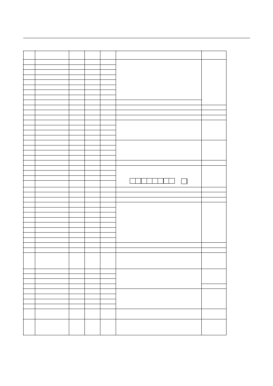
GMS81C4040/87C4060
HYUNDAI
92
May. 2000 Ver 1.0
99
LDA #imm
C4
2
2
Load accumulator
N - - - - - Z -
100
LDA dp
C5
2
3
A
(M)
101
LDA dp + X
C6
2
4
102
LDA !abs
C7
3
4
103
LDA !abs + Y
D5
3
5
104
LDA [dp + X]
D6
2
6
105
LDA [dp]+Y
D7
2
6
106
LDA {X}
D4
1
3
107
LDA {X}+
DB
1
4
X-register auto-increment : A
(M), X
X + 1
108
LDC M.bit
CB
3
4
Load C-flag : C
(M.bit)
- - - - - - - C
109
LDCB M.bit
CB
3
4
Load C-flag with NOT : C
~(M.bit)
- - - - - - - C
110
LDM dp,#imm
E4
3
5
Load memory with immediate data : (M)
imm
- - - - - - - -
111
LDX #imm
1E
2
2
Load X-register
N - - - - - Z -
112
LDX dp
CC
2
3
X
(M)
113
LDX dp + Y
CD
2
4
114
LDX !abs
DC
3
4
115
LDY #imm
3E
2
2
Load X-register
N - - - - - Z -
116
LDY dp
C9
2
3
Y
(M)
117
LDY dp + Y
D9
2
4
118
LDY !abs
D8
3
4
119
LDYA dp
7D
2
5
Load YA : YA
(dp+1)(dp)
N - - - - - Z -
120
LSR A
48
1
2
Logical shift right
N - - - - - ZC
121
LSR dp
49
2
4
122
LSR dp + X
59
2
5
123
LSR !abs
58
3
5
124
MUL
5B
1
9
Multiply : YA
Y x A
N - - - - - Z -
125
NOP
00,FF
1
2
No operation
- - - - - - - -
126
NOT1 M.bit
4B
3
5
Bit complement : (M.bit)
~(M.bit)
- - - - - - - -
127
OR #imm
64
2
2
Logical OR
N - - - - - Z -
128
OR dp
65
2
3
A
A V (M)
129
OR dp + X
66
2
4
130
OR !abs
67
3
4
131
OR !abs + Y
75
3
5
132
OR [dp +X}
76
2
6
133
OR [dp] + Y
77
2
6
134
OR {X}
74
1
3
135
OR1 M.bit
6B
3
5
Bit OR C-flag : C
C V (M.bit)
- - - - - - - C
136
OR1B M.bit
6B
3
5
Bit OR C-flag and NOT : C
C V ~(M.bit)
- - - - - - - C
137
PCALL
4F
2
6
U-page call : M(SP)
(PC
H
), SP
SP -1,
- - - - - - - -
M(SP)
(PC
L
), SP
SP -1,
PC
L
(upage), PC
H
"OFF
H
"
138
POP A
0D
1
4
Pop from stack
- - - - - - - -
139
POP X
2D
1
4
SP
SP + 1, Reg.
M(SP)
140
POP Y
4D
1
4
141
POP PSW
6D
1
4
(restored)
142
PUSH A
0E
1
4
Push to stack
- - - - - - - -
143
PUSH X
2E
1
4
M(SP)
Reg. SP
SP - 1
144
PUSH Y
4E
1
4
145
PUSH PSW
6E
1
4
146
RET
6F
1
5
Return from subroutine :
- - - - - - - -
SP
SP+1, PC
L
M(SP), SP
SP+1, PC
H
M(SP)
147
RETI
7F
1
6
Return from interrupt :
(restored)
SP
SP+1, PSW
M(SP), SP
SP+1,PC
L
M(SP),
SP
SP+1, PC
H
M(SP)
NO.
MNENONIC
OP
CODE
BYTE
NO.
CYCLE
NO
OPERATION
FLAG
NVGBHIZC
7 6 5 4 3 2 1 0 C
"
0
"
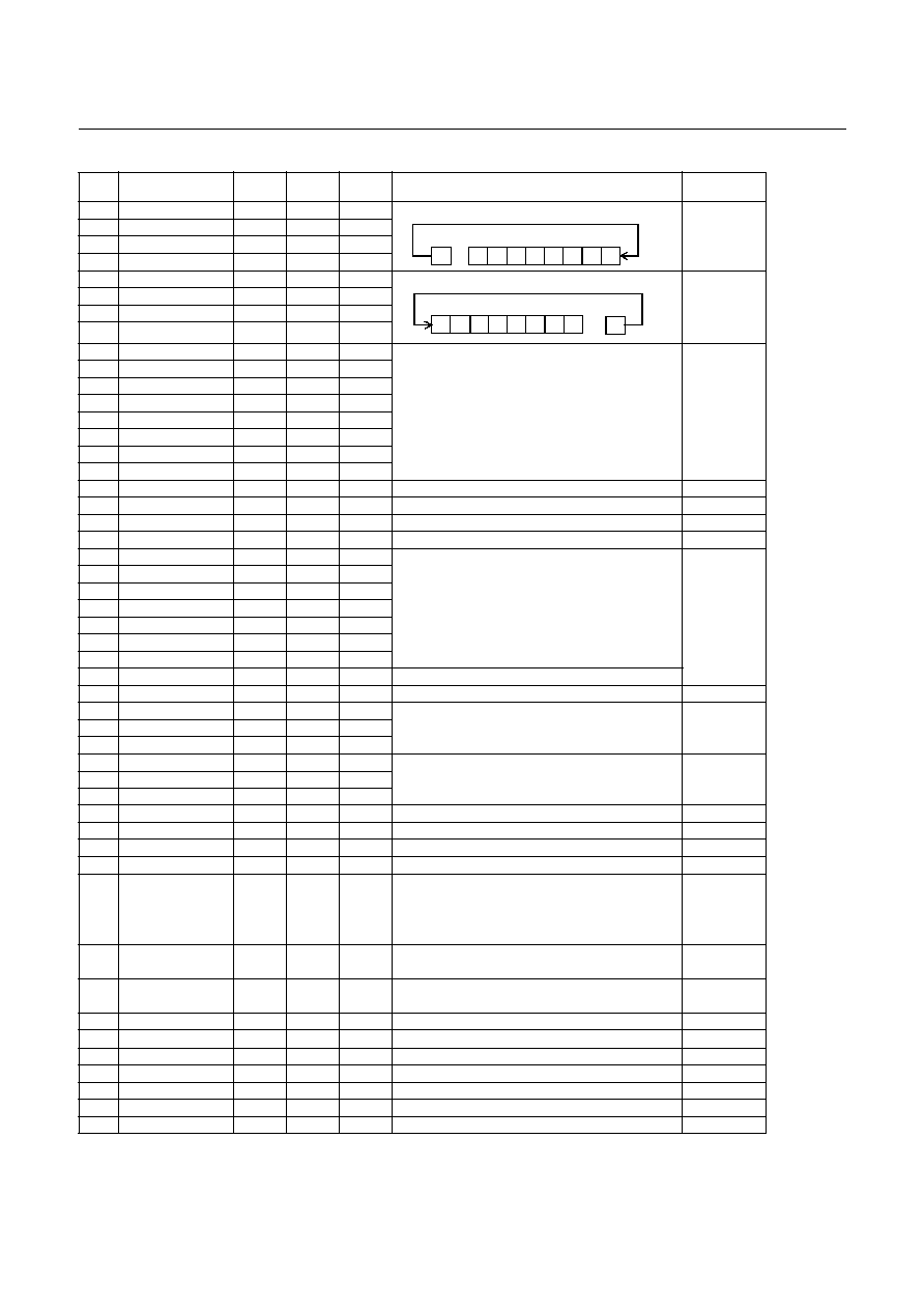
HYUNDAI
GMS81C4040/87C4060
May. 2000 Ver 1.0
93
148
ROL A
28
1
2
Rotate left through carry
N - - - - - ZC
149
ROL dp
29
2
4
150
ROL dp + X
39
2
5
151
ROL !abs
38
3
5
152
ROR A
68
1
2
Rotate right through carry
N - - - - - ZC
153
ROR dp
69
2
4
154
ROR dp + X
79
2
5
155
ROR !abs
78
3
5
156
SBC #imm
24
2
2
Substract with carry
NV - - HZC
157
SBC dp
25
2
3
A
A - (M) - ~(C)
158
SBC dp + X
26
2
4
159
SBC !abs
27
3
4
160
SBC !abs + Y
35
3
5
161
SBC [dp + X]
36
2
6
162
SBC [dp] + Y
37
2
6
163
SBC {X}
34
1
3
164
SET1 dp.bit
x1
2
4
Set bit : (M.bit)
"1"
- - - - - - - -
165
SETA1 A.bit
0B
2
2
Set A.bit : (A.bit)
"1"
- - - - - - - -
166
SETC
A0
1
2
Set C-flag : C
"1"
- - - - - - - 1
167
SETG
C0
1
2
Set G-flag : G
"1"
- - 1 - - - - -
168
STA dp
E5
2
3
Store accumulator contents in memory
- - - - - - - -
169
STA dp + X
E6
2
4
(M)
A
170
STA !abs
E7
3
4
171
STA !abs + Y
F5
3
5
172
STA [dp + X]
F6
2
6
173
STA [dp] + Y
F7
2
6
174
STA {X}
F4
1
3
175
STA {X}+
FB
1
4
X-register auto-increment : (M)
A, X
X + 1
176
STC M.bit
EB
3
6
Store C-flag : (M.bit)
C
- - - - - - - -
177
STX dp
EC
2
4
Store X-register contents in memory
- - - - - - - -
178
STX dp + Y
ED
2
5
(M)
X
179
STX !abs
FC
3
5
180
STY dp
E9
2
4
Store Y-register contents in memory
- - - - - - - -
181
STY dp + X
F9
2
5
(M)
Y
182
STY !abs
F8
3
5
183
STYA dp
DD
2
5
Store YA : (dp+1)(dp)
YA
- - - - - - - -
184
SUBW dp
3D
2
5
16-bits substract without carry : YA
YA - (dp+1)(dp)
NV - - H - ZC
185
TAX
E8
1
2
Transfer accumulator contents to X-register : X
A
N - - - - - Z -
186
TAY
9F
1
2
Transfer accumulator contents to Y-register : Y
A
N - - - - - Z -
187
TCALL n
nA
1
8
Table call :
- - - - - - - -
M(SP)
(PC
H
), SP
SP -1,
M(SP)
(PC
L
), SP
SP -1
PC
L
(Table vector L), PC
H
(Table vector H)
188
TCLR1 !abs
5C
3
6
Test and clear bits with A :
N - - - - - Z -
A - (M), (M)
(M) ^ ~(A)
189
TSET1 !abs
3C
3
6
Test and set bits with A :
N - - - - - Z -
A - (M), (M)
(M) V (A)
190
TSPX
AE
1
2
Transfer stack-pointer contents to X-register : X
SP
N - - - - - Z -
191
TST dp
4C
2
3
Test memory contents for negative or zero : (dp) - 00
H
N - - - - - Z -
192
TXA
C8
1
2
Transfer X-register contents to accumulator : A
X
N - - - - - Z -
193
TXSP
8E
1
2
Transfer X-register contents to stack-pointer : SP
X
N - - - - - Z -
194
TYA
BF
1
2
Transfer Y-register contents to accumulator : A
Y
N - - - - - Z -
195
XAX
EE
1
4
Exchange X-register contents with accumulator : X
f
A
- - - - - - - -
196
XAY
DE
1
4
Exchange Y-register contents with accumulator : Y
f
A
- - - - - - - -
NO.
MNENONIC
OP
CODE
BYTE
NO.
CYCLE
NO
OPERATION
FLAG
NVGBHIZC
C 7 6 5 4 3 2 1 0
7 6 5 4 3 2 1 0 C
GMS81C4040/87C4060
HYUNDAI
94
May. 2000 Ver 1.0
24.3 Instruction Table by Function
1. Arithmetic/Logic Operation
197
XCN
CE
1
5
Exchange nibbles within the accumulator:
N - - - - - Z -
A
7
~ A
4
f
A
3
~ A
0
198
XMA dp
BC
2
5
Exchange memory contents with accumulator
N - - - - - Z -
199
XMA dp + X
AD
2
6
(M)
f
A
200
XMA {X}
BB
1
5
201
XYX
FE
1
4
Exchange X-register contents with Y-register : X
f
Y
- - - - - - - -
NO.
MNENONIC
OP
CODE
BYTE
NO.
CYCLE
NO
OPERATION
FLAG
NVGBHIZC
NO.
MNENONIC
OP
CODE
BYTE
NO.
CYCLE
NO
OPERATION
FLAG
NVGBHIZC
1
ADC #imm
04
2
2
Add with carry.
NV - - H - ZC
2
ADC dp
05
2
3
A
A + (M) + C
3
ADC dp + X
06
2
4
4
ADC !abs
07
3
4
5
ADC !abs+Y
15
3
5
6
ADC [dp+X]
16
2
6
7
ADC [dp]+Y
17
2
6
8
ADC {X}
14
1
3
9
AND #imm
84
2
2
Logical AND
N - - - - - Z -
10
AND dp
85
2
3
A
A ^ (M)
11
AND dp + X
86
2
4
12
AND !abs
87
3
4
13
AND !abs+Y
95
3
5
14
AND [dp+X]
96
2
6
15
AND [dp] + Y
97
2
6
16
AND {X}
94
1
3
17
ASL A
08
1
2
Arithmetic shift left
N - - - - - ZC
18
ASL dp
09
2
4
19
ASL dp + X
19
2
5
20
ASL !abs
18
3
5
21
CMP #imm
44
2
2
Compare accumulator contents with memory contents
N - - - - - ZC
22
CMP dp
45
2
3
A - (M)
23
CMP dp + X
46
2
4
24
CMP !abs
47
3
4
25
CMP !abs + Y
55
3
5
26
CMP [dp + X]
56
2
6
27
CMP [dp] + Y
57
2
6
28
CMP {X}
54
1
3
29
CMPX #imm
5E
2
2
Compare X contents with memory contents
N - - - - - ZC
30
CMPX dp
6C
2
3
X - (M)
31
CMPX !abs
7C
3
4
32
CMPY #imm
7E
2
2
Compare Y contents with memory contents
N - - - - - ZC
33
CMPY dp
8C
2
3
Y - (M)
34
CMPY !abs
9C
3
4
35
COM dp
2C
2
4
1's complement : (dp)
~(dp)
N - - - - - Z -
36
DAA
DF
1
3
Decimal adjust for addition
N - - - - - ZC
37
DAS
CF
1
3
Decimal adjust for substraction
N - - - - - ZC
38
DEC A
A8
1
2
Decrement
N - - - - - Z -
39
DEC dp
A9
2
4
M
M - 1
40
DEC dp + X
B9
2
5
41
DEC !abs
B8
3
5
42
DEC X
AF
1
2
43
DEC Y
BE
1
2
C 7 6 5 4 3 2 1 0
"
0
"
HYUNDAI
GMS81C4040/87C4060
May. 2000 Ver 1.0
95
44
DIV
9B
1
12
Divide : YA/A
Q:A, R:Y
NV - - H - Z -
45
EOR #imm
A4
2
2
Exclusive OR
N - - - - - Z -
46
EOR dp
A5
2
3
A
A
(M)
47
EOR dp + X
A6
2
4
48
EOR !abs
A7
3
4
49
EOR !abs + Y
B5
3
5
50
EOR [ dp + X]
96
2
6
51
EOR [dp] + Y
97
2
6
52
EOR {X}
94
1
3
53
INC A
88
1
2
Increment
N - - - - - ZC
54
INC dp
89
2
4
(M)
(M) + 1
N - - - - - Z -
55
INC dp + X
99
2
5
56
INC !abs
98
3
5
57
INC X
8F
1
2
58
INC Y
9E
1
2
59
LSR A
48
1
2
Logical shift right
N - - - - - ZC
60
LSR dp
49
2
4
61
LSR dp + X
59
2
5
62
LSR !abs
58
3
5
63
MUL
5B
1
9
Multiply : YA
Y x A
N - - - - - Z -
64
OR #imm
64
2
2
Logical OR
N - - - - - Z -
65
OR dp
65
2
3
A
A V (M)
66
OR dp + X
66
2
4
67
OR !abs
67
3
4
68
OR !abs + Y
75
3
5
69
OR [dp +X}
76
2
6
70
OR [dp] + Y
77
2
6
71
OR {X}
74
1
3
72
ROL A
28
1
2
Rotate left through carry
N - - - - - ZC
73
ROL dp
29
2
4
74
ROL dp + X
39
2
5
75
ROL !abs
38
3
5
76
ROR A
68
1
2
Rotate right through carry
N - - - - - ZC
77
ROR dp
69
2
4
78
ROR dp + X
79
2
5
79
ROR !abs
78
3
5
80
SBC #imm
24
2
2
Substract with carry
NV - - HZC
81
SBC dp
25
2
3
A
A - (M) - ~(C)
82
SBC dp + X
26
2
4
83
SBC !abs
27
3
4
84
SBC !abs + Y
35
3
5
85
SBC [dp + X]
36
2
6
86
SBC [dp] + Y
37
2
6
87
SBC {X}
34
1
3
88
TST dp
4C
2
3
Test memory contents for negative or zero : (dp) - 00
H
N - - - - - Z -
89
XCN
CE
1
5
Exchange nibbles within the accumulator:
N - - - - - Z -
A
7
~ A
4
f
A
3
~ A
0
NO.
MNENONIC
OP
CODE
BYTE
NO.
CYCLE
NO
OPERATION
FLAG
NVGBHIZC
7 6 5 4 3 2 1 0 C
"
0
"
C 7 6 5 4 3 2 1 0
7 6 5 4 3 2 1 0 C
GMS81C4040/87C4060
HYUNDAI
96
May. 2000 Ver 1.0
2. Register / Memory Operation
3. 16-Bit Operation
NO.
MNENONIC
OP
CODE
BYTE
NO.
CYCLE
NO
OPERATION
FLAG
NVGBHIZC
1
LDA #imm
C4
2
2
Load accumulator
N - - - - - Z -
2
LDA dp
C5
2
3
A
(M)
3
LDA dp + X
C6
2
4
4
LDA !abs
C7
3
4
5
LDA !abs + Y
D5
3
5
6
LDA [dp + X]
D6
2
6
7
LDA [dp]+Y
D7
2
6
8
LDA {X}
D4
1
3
9
LDA {X}+
DB
1
4
X-register auto-increment : A
(M), X
X + 1
10
LDM dp,#imm
E4
3
5
Load memory with immediate data : (M)
imm
- - - - - - - -
11
LDX #imm
1E
2
2
Load X-register
N - - - - - Z -
12
LDX dp
CC
2
3
X
(M)
13
LDX dp + Y
CD
2
4
14
LDX !abs
DC
3
4
15
LDY #imm
3E
2
2
Load X-register
N - - - - - Z -
16
LDY dp
C9
2
3
Y
(M)
17
LDY dp + Y
D9
2
4
18
LDY !abs
D8
3
4
19
STA dp
E5
2
3
Store accumulator contents in memory
- - - - - - - -
20
STA dp + X
E6
2
4
(M)
A
21
STA !abs
E7
3
4
22
STA !abs + Y
F5
3
5
23
STA [dp + X]
F6
2
6
24
STA [dp] + Y
F7
2
6
25
STA {X}
F4
1
3
26
STA {X}+
FB
1
4
X-register auto-increment : (M)
A, X
X + 1
27
STX dp
EC
2
4
Store X-register contents in memory
- - - - - - - -
28
STX dp + Y
ED
2
5
(M)
X
29
STX !abs
FC
3
5
30
STY dp
E9
2
4
Store Y-register contents in memory
- - - - - - - -
31
STY dp + X
F9
2
5
(M)
Y
32
STY !abs
F8
3
5
33
TAX
E8
1
2
Transfer accumulator contents to X-register : X
A
N - - - - - Z -
34
TAY
9F
1
2
Transfer accumulator contents to Y-register : Y
A
N - - - - - Z -
35
TSPX
AE
1
2
Transfer stack-pointer contents to X-register : X
SP
N - - - - - Z -
36
TXA
C8
1
2
Transfer X-register contents to accumulator : A
X
N - - - - - Z -
37
TXSP
8E
1
2
Transfer X-register contents to stack-pointer : SP
X
N - - - - - Z -
38
TYA
BF
1
2
Transfer Y-register contents to accumulator : A
Y
N - - - - - Z -
39
XAX
EE
1
4
Exchange X-register contents with accumulator : X
f
A
- - - - - - - -
40
XAY
DE
1
4
Exchange Y-register contents with accumulator : Y
f
A
- - - - - - - -
41
XMA dp
BC
2
5
Exchange memory contents with accumulator
N - - - - - Z -
42
XMA dp + X
AD
2
6
(M)
f
A
43
XMA {X}
BB
1
5
44
XYX
FE
1
4
Exchange X-register contents with Y-register : X
f
Y
- - - - - - - -
NO.
MNENONIC
OP
CODE
BYTE
NO.
CYCLE
NO
OPERATION
FLAG
NVGBHIZC
1
ADDW dp
1D
2
5
16-bits add without carry : YA
YA + (dp+1)(dp)
NV - - H - ZC
2
CMPW dp
5D
2
4
Compare YA contents with memory pair contents :
N - - - - - ZC
YA - (dp+1)(dp)
3
DECW dp
BD
2
6
Decrement memory pair : (dp+1)(dp)
{(dp+1)(dp)} - 1
N - - - - - Z -
4
INCW dp
9D
2
6
Increment memory pair : (dp+1)(dp)
{(dp+1)(dp)} + 1
N - - - - - Z -
HYUNDAI
GMS81C4040/87C4060
May. 2000 Ver 1.0
97
4. Bit Manipulation
5. Branch / Jump Operation
5
LDYA dp
7D
2
5
Load YA : YA
(dp+1)(dp)
N - - - - - Z -
6
STYA dp
DD
2
5
Store YA : (dp+1)(dp)
YA
- - - - - - - -
7
SUBW dp
3D
2
5
16-bits substract without carry : YA
YA - (dp+1)(dp)
NV - - H - ZC
NO.
MNENONIC
OP
CODE
BYTE
NO.
CYCLE
NO
OPERATION
FLAG
NVGBHIZC
NO.
MNENONIC
OP
CODE
BYTE
NO.
CYCLE
NO
OPERATION
FLAG
NVGBHIZC
1
AND1 M.bit
8B
3
4
Bit AND C-flag : C
C ^ (M.bit)
- - - - - - - C
2
AND1B M.bit
8B
3
4
Bit AND C-flag and NOT : C
C ^ ~(M.bit)
- - - - - - - C
3
BIT dp
0C
2
4
Bit test A with memory :
MM - - - - Z -
4
BIT !abs
1C
3
5
Z
A ^ M, N
(M
7
), V
(M
6
)
5
CLR1 dp.bit
y1
2
4
Clear bit : (M.bit)
"0"
- - - - - - - -
6
CLR1A A.bit
2B
2
2
Clear A.bit : (A.bit)
"0"
- - - - - - - -
7
CLRC
20
1
2
Clear C-flag : C
"0"
- - - - - - - 0
8
CLRG
40
1
2
Clear G-flag : G
"0"
- - 0 - - - - -
9
CLRV
80
1
2
Clear V-flag : V
"0"
- 0 - - 0 - - -
10
EOR1 M.bit
AB
3
5
Bit exclusive-OR C-flag : C
C
(M.bit)
- - - - - - - C
11
EOR1B M.bit
AB
3
5
Bit exclusive-OR C-flag and NOT : C
C
(M.bit)
- - - - - - - C
12
LDC M.bit
CB
3
4
Load C-flag : C
(M.bit)
- - - - - - - C
13
LDCB M.bit
CB
3
4
Load C-flag with NOT : C
~(M.bit)
- - - - - - - C
14
NOT1 M.bit
4B
3
5
Bit complement : (M.bit)
~(M.bit)
- - - - - - - -
15
OR1 M.bit
6B
3
5
Bit OR C-flag : C
C V (M.bit)
- - - - - - - C
16
OR1B M.bit
6B
3
5
Bit OR C-flag and NOT : C
C V ~(M.bit)
- - - - - - - C
17
SET1 dp.bit
x1
2
4
Set bit : (M.bit)
"1"
- - - - - - - -
18
SETA1 A.bit
0B
2
2
Set A.bit : (A.bit)
"1"
- - - - - - - -
19
SETC
A0
1
2
Set C-flag : C
"1"
- - - - - - - 1
20
SETG
C0
1
2
Set G-flag : G
"1"
- - 1 - - - - -
21
STC M.bit
EB
3
6
Store C-flag : (M.bit)
C
- - - - - - - -
22
TCLR1 !abs
5C
3
6
Test and clear bits with A :
N - - - - - Z -
A - (M), (M)
(M) ^ ~(A)
23
TSET1 !abs
3C
3
6
Test and set bits with A :
N - - - - - Z -
A - (M), (M)
(M) V (A)
NO.
MNENONIC
OP
CODE
BYTE
NO.
CYCLE
NO
OPERATION
FLAG
NVGBHIZC
1
BBC A.bit,rel
y2
2
4/6
Branch if bit clear :
- - - - - - - -
2
BBC dp.bit,rel
y3
3
5/7
if(bit) = 0, then PC
PC + rel
3
BBS A.bit,rel
x2
2
4/6
Branch if bit clear :
- - - - - - - -
4
BBS dp.bit,rel
x3
3
5/7
if(bit) = 1, then PC
PC + rel
5
BCC rel
50
2
2/4
Branch if carry bit clear :
if(C) = 0, then PC
PC + rel
MM - - - - Z -
6
BCS rel
D0
2
2/4
Branch if carry bit set : If (C) =1, then PC
PC + rel
- - - - - - - -
7
BEQ rel
F0
2
2/4
Branch if equal : if (Z) = 1, then PC
PC + rel
- - - - - - - -
8
BMI rel
90
2
2/4
Branch if munus : if (N) = 1, then PC
PC + rel
- - - - - - - -
9
BNE rel
70
2
2/4
Branch if not equal : if (Z) = 0, then PC
PC + rel
- - - - - - - -
10
BPL rel
10
2
2/4
Branch if not minus : if (N) = 0, then PC
PC + rel
- - - - - - - -
11
BRA rel
2F
2
4
Branch always : PC
PC + rel
- - - - - - - -
12
BVC rel
30
2
2/4
Branch if overflow bit clear :
- - - - - - - -
If (V) = 0, then PC
PC + rel
13
BVS rel
B0
2
2/4
Branch if overflow bit set :
- - - - - - - -
If (V) = 1, then PC
PC + rel
GMS81C4040/87C4060
HYUNDAI
98
May. 2000 Ver 1.0
6. Control Operation & etc.
14
CALL !abs
3B
3
8
Subroutine call
- - - - - - - -
15
CALL [dp]
5F
2
8
M(SP)
(PC
H
), SP
SP-1, M(SP)
(PC
L
), SP
SP-1
if !abs, PC
abs ; if [dp], PC
L
(dp), PC
H
(dp+1)
16
CBNE dp,rel
FD
3
5/7
Compare and branch if not equal ;
- - - - - - - -
17
CBNE dp + X, rel
8D
3
6/8
If A
(M), then PC
PC + rel.
18
DBNE dp,rel
AC
3
5/7
Decrement and branch if not equal :
- - - - - - - -
19
DBNE Y,rel
7B
2
4/6
if (M)
0, then PC
PC + rel.
20
JMP !abs
1B
3
3
Unconditional jump
- - - - - - - -
21
JMP [!abs]
1F
3
5
PC
jump address
22
JMP [dp]
3F
2
4
23
PCALL
4F
2
6
U-page call : M(SP)
(PC
H
), SP
SP -1,
- - - - - - - -
M(SP)
(PC
L
), SP
SP -1,
PC
L
(upage), PC
H
"OFF
H
"
24
TCALL n
nA
1
8
Table call :
- - - - - - - -
M(SP)
(PC
H
), SP
SP -1,
M(SP)
(PC
L
), SP
SP -1
PC
L
(Table vector L), PC
H
(Table vector H)
NO.
MNENONIC
OP
CODE
BYTE
NO.
CYCLE
NO
OPERATION
FLAG
NVGBHIZC
NO.
MNENONIC
OP
CODE
BYTE
NO.
CYCLE
NO
OPERATION
FLAG
NVGBHIZC
1
BRK
0F
1
8
Software interrupt:
- - - 1 - 0 - -
B
"1", M(SP)
(PC
H
), SP
SP - 1,
M(s)
(PC
L
), SP
S - 1, M(SP)
PSW,
SP
SP - 1, PC
L
(0FFDE
H
), PC
H
(0FFDF
H
)
2
DI
60
1
3
Disable interrupts : I
"0"
- - - - - 0 - -
3
EI
E0
1
3
Enable interrupts : I
"1"
- - - - - 1 - -
4
NOP
FF
1
2
No operation
- - - - - - - -
5
POP A
0D
1
4
Pop from stack
- - - - - - - -
6
POP X
2D
1
4
SP
SP + 1, Reg.
M(SP)
7
POP Y
4D
1
4
8
POP PSW
6D
1
4
(restored)
9
PUSH A
0E
1
4
Push to stack
- - - - - - - -
10
PUSH X
2E
1
4
M(SP)
Reg. SP
SP - 1
11
PUSH Y
4E
1
4
12
PUSH PSW
6E
1
4
13
RET
6F
1
5
Return from subroutine :
- - - - - - - -
SP
SP+1, PC
L
M(SP), SP
SP+1, PC
H
M(SP)
14
RETI
7F
1
6
Return from interrupt :
(restored)
SP
SP+1, PSW
M(SP), SP
SP+1,PC
L
M(SP),
SP
SP+1, PC
H
M(SP)
Document Outline
- GMS81C4040/GMS87C4060
- 1. OVERVIEW
- 2. BLOCK DIAGRAM
- 3. PIN ASSIGNMENT
- 4. PACKAGE DIAGRAM
- 5. PIN FUNCTION
- 6. PORT STRUCTURES
- RESET
- TEST
- XIN, XOUT
- OSC1, OSC2
- R00~07, R53
- R10~15 (AN0~5)
- R16, 17, 20, 24, 25, 26, 27, 52, 67
- R21/Sclk, R22/Sout
- R23/Sin
- R40~43 (PWM0~3)
- R44, 45, 46, 47 (SCL, SDA, PWM)
- R50/BUZZ, R51/PWM8
- R54/YM, R55/YS, R56/I
- R, G, B
- 7. ELECTRICAL CHARACTERISTICS
- 8. MEMORY ORGANIZATION
- 9. I/O PORTS
- 10. CLOCK GENERATOR
- 11. TIMER
- 12. A/D Converter
- 13. Serial I/O
- 14. Pulse Width Modulation (PWM)
- 15. Interrupt interval measurement circuit
- 16. Buzzer driver
- 17. On Screen Display (OSD)
- 18. I2C Bus Interface
- 19. INTERRUPTS
- 20. WATCHDOG TIMER
- 21. OSCILLATOR CIRCUIT
- 22. RESET
- 23. OTP Programming
- 24. Assemble mnemonics