Äîêóìåíòàöèÿ è îïèñàíèÿ www.docs.chipfind.ru

HYNIX SEMICONDUCTOR INC.
8-BIT SINGLE-CHIP MICROCONTROLLERS
GMS81C7008
GMS81C7016
User's Manual
(Ver. 2.01)

Version 2.01
Published by
MCU Application Team
©
©
©
©
2001 Hynix semiconductor Inc. All right reserved.
Additional information of this manual may be served by Hynix semiconductor offices in Korea or Distributors and Representatives listed
at address directory.
Hynix semiconductor reserves the right to make changes to any information here in at any time without notice.
The information, diagrams and other data in this manual are correct and reliable; however, Hynix semiconductor is in no way responsible
for any violations of patents or other rights of the third party generated by the use of this manual.
REVISION HISTORY
VERSION 2.01 (APR., 2001) This book
Delete product of 52SDIP package also, no longer produce 52pin MCU.
The compay name Hyundai Electronics Industires Co., Ltd. changed to Hynix Semiconductor Inc.
VERSION 2.00 (FEB., 2001)
Delete product of 52LQFP package.
Fixed some errata that pin number 25 and 26 on 52SDIP package are reversed.
VERSION 1.02 (NOV., 2000)
Fixed the name of LCR register on page 39 and 75, the BUR register on page 66.
VERSION 1.01 (SEP., 2000) sticker
Correct the bit LVDE of LVDR register on page 91.

GMS81C7008/7016/7108/7116
APR., 2001 Ver 2.01
Table of Contents
1. OVERVIEW............................................1
Description .........................................................1
Features .............................................................1
Development Tools ............................................2
Ordering Information ..........................................2
2. BLOCK DIAGRAM .................................3
3. PIN ASSIGNMENT ................................4
4. PACKAGE DIMENSION ........................5
5. PIN FUNCTION......................................6
6. PORT STRUCTURES............................9
7. ELECTRICAL CHARACTERISTICS ....11
Absolute Maximum Ratings .............................11
Recommended Operating Conditions ..............11
DC Electrical Characteristics ...........................11
A/D Converter Characteristics .........................13
AC Characteristics ...........................................13
Serial Interface Timing Characteristics ............15
Typical Characteristics .....................................16
8. MEMORY ORGANIZATION.................18
Registers ..........................................................18
Program Memory .............................................21
Data Memory ...................................................24
List of Control Registers ...................................25
Addressing Mode .............................................28
9. I/O PORTS ...........................................32
Registers for Port .............................................32
I/O Ports Configuration ....................................33
10. CLOCK GENERATOR .......................37
11. OPERATION MODE ..........................39
Operation Mode Switching ...............................40
12. BASIC INTERVAL TIMER..................42
13. TIMER/EVENT COUNTER ................44
8-bit Timer / Counter Mode ..............................47
16-bit Timer / Counter Mode ............................51
8-bit Capture Mode ..........................................52
16-bit Capture Mode ........................................53
Timer output port mode ....................................53
PWM Mode ......................................................54
14. ANALOG DIGITAL CONVERTER .....57
15. SERIAL COMMUNICATION ..............59
Transmission/Receiving Timing ...................... 60
The method of Serial I/O ................................. 61
The Method to Test Correct Transmission ...... 61
16. BUZZER FUNCTION .........................62
17. INTERRUPTS ....................................64
Interrupt Sequence .......................................... 66
BRK Interrupt .................................................. 67
Multi Interrupt .................................................. 67
External Interrupt ............................................. 68
Key Scan Interrupt .......................................... 68
18. LCD DRIVER .....................................70
LCD Control Registers .................................... 70
Duty and Bias Selection of LCD driver ............ 72
Selecting Frame Frequency ............................ 72
LCD Display Memory ...................................... 75
Control Method of LCD Driver ......................... 76
19. WATCH / WATCHDOG TIMER .........78
Watch Timer .................................................... 78
Watchdog Timer .............................................. 78
20. POWER DOWN OPERATION...........81
SLEEP Mode ................................................... 81
STOP Mode .................................................... 82
21. OSCILLATOR CIRCUIT.....................85
22. RESET ...............................................86
External Reset Input ........................................ 86
Watchdog Timer Reset ................................... 86
23. POWER FAIL PROCESSOR.............87
24. DEVELOPMENT TOOLS...................89
OTP Programming .......................................... 89
Emulator EVA. Board Setting .......................... 90
Appendix
A. MASK ORDER SHEET .......................... i
B. INSTRUCTION ...................................... ii
Terminology List .................................................ii
Instruction Map .................................................. iii

GMS81C7008/7016/7108/7116
APR., 2001 Ver 2.01
Instruction Set ................................................... iv
C. SOFTWARE EXAMPLE ........................ x
GMS81C7008/7016
APR., 2001 Ver 2.01
1
GMS81C7008/16
CMOS SINGLE-CHIP 8-BIT MICROCONTROLLER
WITH LCD DRIVER & A/D CONVERTER
1. OVERVIEW
1.1 Description
The GMS81C7008/7016 is advanced CMOS 8-bit microcontrollers with 8K/16K bytes of ROM. There are a powerful microcontroller
which provides a highly flexible and cost effective solution to many LCD applications. These provide the following standard features:16K/
8K bytes of mask type ROM or 16K bytes OTP ROM, 448 bytes of RAM, 8-bit timer/counter, 8-bit A/D converter, 10 bit high speed PWM
Output, programmable buzzer driving port, 8-bit basic interval timer, watch dog timer, serial peripheral interface, on chip oscillator and
clock circuitry. They also come with 4com/24seg LCD driver. In addition, it support power saving mode to reduce power consumption.
1.2 Features
· 8K/16K Bytes On-chip Programmable ROM
· 448 Bytes of On-chip Data RAM
(Included stack area and 27 nibbles LCD Display
RAM)
· Instruction Execution Time
1
µ
s at 4MHz (2cycle NOP Instruction)
· One 8-bit Basic Interval Timer
· One Watch Timer
· One Watchdog Timer
· Four 8-bit Timer/Event Counter
(or Two 16-bit Timer/Event Counter)
· Two channel 10-bit High Speed PWM Output
· Three External Interrupt input ports
· One Programmable 6-bit Buzzer Driving port
- 500Hz ~ 250kHz@4MHz
· 49 I/O Ports
· Eight channel 8-bit A/D converter
· One 8-bit Serial Communication Interface
· LCD Display/ Controller
- Static Mode (27SEG x 1COM, Static)
- 1/2 Duty Mode (26SEG x 2COM, 1/2 or 1/3 Bias)
- 1/3 Duty Mode (25SEG x 3COM, 1/3 Bias)
- 1/4 Duty Mode (24SEG x 4COM, 1/3 Bias)
- Internal Built-in Resistor Circuit for Bias
· Thirteen Interrupt sources
- Basic Interval Timer: 1
- External input: 3
- Timer/Event counter: 4
- ADC: 1
- Serial Interface: 1
- WT:1
- WDT: 1
- Key Scan: 1
· Main Clock Oscillation (1.0~4.5MHz)
- Crystal
- Ceramic Resonator
- External R Oscillator (Built-in Capacitor)
· Sub Clock Oscillation
- 32.768kHz Crystal Oscillator
· Power Saving Operation Mode
- Main / Sub Active mode changeable
- 2/8/16/64 divided system clock selectable
· Power Down Mode
- STOP mode
- SLEEP mode
- Sub active Mode
· 2.7V to 5.5V Wide Operating Voltage Range
· Noise Immunity Circuit for EMS
Device name
ROM Size
RAM Size
I/O
OTP
Package
GMS81C7008
8K bytes
448 bytes
49
GMS87C7016
64SDIP, 64MQFP
GMS81C7016
16K bytes
448 bytes
49
GMS87C7016
GMS81C7008/7016
2
APR., 2001 Ver 2.01
- Power fail processor
- Built in Noise filter
· 64SDIP, 64LQFP package types
· Available 16K bytes OTP version
1.3 Development Tools
Note: There are several setting switches in the Emulator.
User should read carefully and do setting properly before
developing the program refer to "24.2 Emulator EVA. Board
Setting" on page 90. Otherwise, the Emulator may not work
properly.
The GMS81C7008/16 is supported by a full-featured macro as-
sembler, an in-circuit emulator CHOICE-Dr.
TM
and OTP pro-
grammers. There are two different type programmers, one is
single type, another is gang type. For more detail, refer to OTP
Programming chapter. Macro assembler operates under the MS-
Windows 95/98
TM
.
Please contact sales part of Hynix semiconductor.
1.4 Ordering Information
Software
- MS- Window base assembler
- Linker / Editor / Debugger
Hardware
(Emulator)
- CHOICE-Dr.
- CHOICE-Dr. EVA 81C51/81C7X B/D
OTP program-
mer
- CHOICE-SIGMA (Single type)
- CHOICE-GANG4 (4-gang type)
Device name
ROM Size (bytes)
RAM size
Package
Mask ROM version
GMS81C7008 K
GMS81C7016 K
GMS81C7008 Q
GMS81C7016 Q
8K bytes
16K bytes
8K bytes
16K bytes
448 bytes
448 bytes
448 bytes
448 bytes
64SDIP
64SDIP
64MQFP
64MQFP
OTP ROM version
GMS87C7016 K
GMS87C7016 Q
16K bytes OTP
16K bytes OTP
448 bytes
448 bytes
64SDIP
64MQFP
GMS81C7008/7016
APR., 2001 Ver 2.01
3
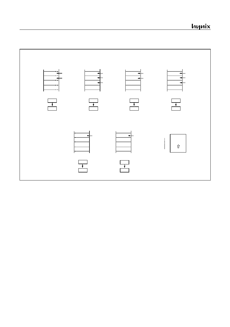
2. BLOCK DIAGRAM
GMS81C7008/7016
ALU
LCD Controller / Driver (LCDC)
Accumulator
Stack Pointer
Interrupt Controller
Data
Memory
LCD Display
Memory
Program
Memory
Data Table
PC
8-bit Basic
Interval Tim er
High Speed
PC
R1
R0
R3
Buzzer
Driver
PSW
System controller
Timing generator
System
Clock Controller
Clock
Generator
High freq.
Low freq.
RESET
XIN
XOUT
SXIN
SXOUT
Common Drive Output
COM0
R00 / INT0
R01 / INT1
R02 / INT2
R03 / EC0
R04 / EC2
R05 / SCK
R06 / SO
R07 / SI
R10
R11
R30 / BUZ
VDD
VSS
Power
Supply
VCL0
VCL1
VCL2
COM1/SEG26
COM2/SEG25
COM3/SEG24
LCD Power
Control Circuit
AVDD
AVSS
Power
Supply
Circuit
BIAS
R20 / AN0
R31 / PWM0 / T1O
R32 / PWM1 / T3O
R33
R21 / AN1
R22 / AN2
R23 / AN3
8-bit
A /D C onverter
R2
PWM
8-bit
Tim er/C ounter
SIO
R24 / AN4
R25 / AN5
R26 / AN6
R27 / AN7
R4
R5
R6
R34 / WDTO
Watch/
Timer
R35 / SXOUT
R36 / SXIN
Segment Drive Output
SEG0 ~ SEG23
R40-R47
Watchdog
Key
Scan
R50-R56
R60-R67
LCD Power
Supply
GMS81C7008/7016
4
APR., 2001 Ver 2.01
3. PIN ASSIGNMENT
VCL0
VCL1
VCL2
AV
DD
R20
R21
R22
R23
AV
SS
BIAS
X
IN
X
OUT
RESET
R36
R35
V
SS
AN0
AN1
AN2
AN3
PWM1 / T3O
PWM0 / T1O
BUZ
WDTO
R24
R25
R26
R27
R07
R06
R05
R04
R03
R02
R01
R00
R11
R10
R34
R33
SI
SO
EC2
EC0
INT2
INT1
INT0
V
DD
COM3
COM2
COM1
COM0
R67
R66
R65
R64
R63
R62
R61
R60
R57
R56
R55
R54
R53
R52
R51
R50
R47
R46
R45
R44
R43
R42
R41
R40
R30
R31
R32
R21
R66
R67
COM0
COM1
COM2
COM3
V
DD
VCL0
VCL1
VCL2
AV
DD
R20
AN1
SEG22
R02
R42
R41
R40
R30
R31
R32
R33
R34
R10
R11
R00
R01
INT2
INT0
INT1
R6
5
R6
3
R6
2
R6
1
R6
0
R5
7
R5
6
R5
5
R5
4
R5
3
R5
2
R5
1
R5
0
R4
7
R4
6
R4
5
R6
4
R4
4
R4
3
R2
2
AV
SS
BI
AS
XI
N
XO
UT
RESET
R3
6
R3
5
V
SS
R2
4
R2
5
R2
6
R2
7
R0
7
R0
6
R0
5
R2
3
R0
4
R0
3
AN2
SX
IN
SX
OU
T
AN4
AN5
AN6
AN7
SI
SO
SCK
AN3
EC2
EC0
1
2
3
4
5
6
7
8
9
10
11
12
13
14
15
16
17
18
19
48
47
46
45
44
43
42
41
40
39
38
37
36
35
34
33
51
50
49
32
31
30
29
28
27
26
25
24
23
22
21
20
52
53
54
55
56
57
58
59
60
61
62
63
64
64MQFP
64SDIP
1
2
3
4
5
6
7
8
9
10
11
12
13
14
15
16
17
18
19
20
21
22
23
24
25
26
27
28
29
30
31
32
64
63
62
61
60
59
58
57
56
55
54
53
52
51
50
49
48
47
46
45
44
43
42
41
40
39
38
37
36
35
34
33
GMS
8
1C
7
008
/70
1
6
GMS81C7008/7016
(Top View)
(Top View)
AN4
AN5
AN6
AN7
SX
IN
SX
OUT
SCK
SEG0
SEG1
SEG2
SEG3
SEG4
SEG5
SEG6
SEG7
SEG8
SEG9
SEG10
SEG11
SEG12
SEG13
SEG14
SEG15
SEG16
SEG17
SEG18
SEG19
SEG20
SEG21
SEG22
SEG23
SEG26
SEG25
SEG24
WDTO
PWM1/T3O
PWM0/T1O
BUZ
SEG0
SEG1
SEG2
SE
G
3
SE
G
4
SE
G
5
SE
G
6
SEG
7
SE
G
8
SE
G
9
SE
G
1
0
SE
G
1
1
SEG
1
2
SEG
1
3
SEG
1
4
SEG
1
5
SEG
1
6
SE
G
1
7
SEG
1
8
SEG
1
9
SEG
2
0
SEG
2
1
SEG23
AN0
SEG26
SEG25
SEG24
KS1
KS0
KS0
KS1
GMS81C7008/7016
APR., 2001 Ver 2.01
5
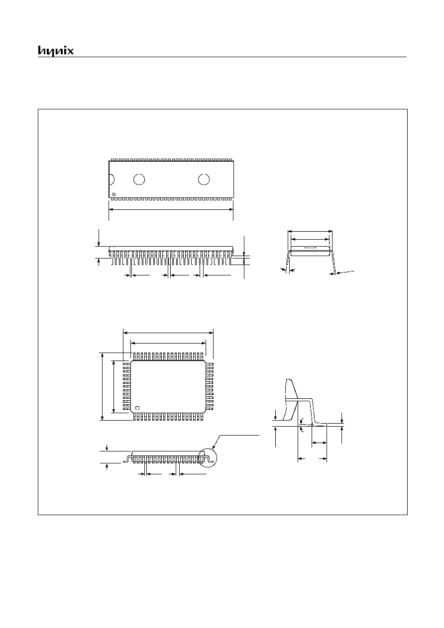
4. PACKAGE DIMENSION
UNIT: INCH
2.280
2.260
0.022
0.016
0.050
0.030
0.070 Typ.
0.1
4
0
0.1
2
0
mi
n
.
0.
015
0.680
0.660
0.750 Typ.
0-15
°
64SDIP
0.012
0.008
0
.
20
5 m
a
x.
20.10
19.90
24.15
23.65
18.1
5
17.6
5
14.1
0
13.9
0
3.18 max.
0.50
0.35
1.00 Typ.
SEE DETAIL "A"
1.03
0.73
0-7
°
0.
36
0.
10
0.
23
0.
13
1.95
REF
DETAIL "A"
UNIT: MM
64MQFP

GMS81C7008/7016
6
APR., 2001 Ver 2.01
5. PIN FUNCTION
V
DD
: Supply voltage.
V
SS
: Circuit ground.
RESET: Reset the MCU.
AV
DD
: Supply voltage to the ladder resistor of ADC circuit. To
enhance the resolution of analog to digital converter, use inde-
pendent power source as well as possible, other than digital pow-
er source.
AV
SS
: ADC circuit ground.
X
IN
: Input to the inverting oscillator amplifier and input to the in-
ternal main clock operating circuit.
X
OUT
: Output from the inverting oscillator amplifier.
BIAS: LCD bias voltage input pin.
VCL0~VCL2: LCD driver power supply pins. The voltage on
each pin is VCL2
>
VCL1
>
VCL0. For details, Refer to "18. LCD
DRIVER" on page 70.
COM0~COM3: LCD common signal output pins. Also, the pins
of COM1,COM2 and COM3 are shared with LCD segment sig-
nal outputs of SEG26, SEG25, SEG24 as application require-
ment.
SX
IN
: Input to the internal subsystem clock operating circuit. In
addition, SX
IN
is shared with the R36 which is selected by the
software option.
SX
OUT
: Output from the inverting subsystem oscillator amplifi-
er. In addition, SX
OUT
is shared with the R35 which is selected
by the software option.
R00~R07: R0 is an 8-bit CMOS bidirectional I/O port. R0 pins 1
or 0 written to the Port Direction Register can be used as outputs
or schmitt trigger inputs. Also, pull-up resistors and open-drain
outputs are software assignable.
In addition, R0 serves the functions of the various following spe-
cial features.
R10~R11: R1 is a 2-bit CMOS bidirectional I/O port. R1 pins 1
or 0 written to the Port Direction Register can be used as outputs
or inputs. Also, pull-up resistors and open-drain outputs are soft-
ware assignable. These pins are not served on 81C71XX.
In addition, R0 serves the functions of the various following spe-
cial features.
R20~R27: R2 is an 8-bit CMOS bidirectional I/O port. R2 pins 1
or 0 written to the Port Direction Register can be used as outputs
or inputs. Also, pull-up resistors and open-drain outputs are soft-
ware assignable.R24~R27 are not served on 81C71XX.
In addition, R2 is shared with the ADC input.
R30~R36: R3 is a 7-bit CMOS bidirectional I/O port. R3 pins 1
or 0 written to the Port Direction Register can be used as outputs
or inputs. Also, pull-up resistors and open-drain outputs are soft-
ware assignable. R33, R34 are not served on 81C71XX.
In addition, R3 serves the functions of the various follow-
ing special features.
SEG0~SEG7: These pins generate LCD segment signal output.
Every LCD segment pins are shared with normal R4 input/output
port. R4 is an 8-bit CMOS bidirectional I/O port. R4 pins 1 or 0
written to the Port Direction Register can be used as outputs or in-
Port pin
Alternate function
R00
R01
R02
R03
R04
R05
R06
R07
INT0 (External interrupt 0)
INT1 (External interrupt 1)
INT2 (External interrupt 2)
EC0 (Event counter input 0)
EC2 (Event counter input 2)
SCK (Serial clock)
SO (Serial data output)
SI (Serial data input)
Port pin
Alternate function
R00
R01
KS0 (Key scan 0)
KS1 (Key scan 1)
Port pin
Alternate function
R20
R21
R22
R23
R24
R25
R26
R27
AN0 (Analog Input 0)
AN1 (Analog Input 1)
AN2 (Analog Input 2)
AN3 (Analog Input 3)
AN4 (Analog Input 4)
AN5 (Analog Input 5)
AN6 (Analog Input 6)
AN7 (Analog Input 7)
Port pin
Alternate function
R30
R31
R32
R33
R34
R35
R36
BUZ (Buzzer driving output)
PWM0 / T1O (PWM 0 output
/ Timer 1 output)
PWM1 /T3O (PWM 1 output
/ Timer 3 output)
-
WDTO (Watchdog timer output)
SX
OUT
(Sub clock output)
SX
IN
(Sub clock input)

GMS81C7008/7016
APR., 2001 Ver 2.01
7
puts.
SEG8~SEG15: These pins generate LCD segment signal output.
Every LCD segment pins are shared with normal R5 input/output
port. R5 is an 8-bit CMOS bidirectional I/O port. R5 pins 1 or 0
written to the Port Direction Register can be used as outputs or in-
puts.
SEG16~SEG23: These pins generate LCD segment signal out-
put.
Every LCD segment pins are shared with normal R6 input/output
port. R6 is an 8-bit CMOS bidirectional I/O port. R6 pins 1 or 0
written to the Port Direction Register can be used as outputs or in-
puts.
LCD pin function
Port pin
SEG0 (LCD segment 0 signal output)
SEG1 (LCD segment 1 signal output)
SEG2 (LCD segment 2 signal output)
SEG3 (LCD segment 3 signal output)
SEG4 (LCD segment 4 signal output)
SEG5 (LCD segment 5 signal output)
SEG6 (LCD segment 6 signal output)
SEG7 (LCD segment 7 signal output)
R40
R41
R42
R43
R44
R45
R46
R47
LCD pin function
Port pin
SEG8 (LCD segment 8 signal output)
SEG9 (LCD segment 9 signal output)
SEG10 (LCD segment 10 signal output)
SEG11 (LCD segment 11 signal output)
SEG12 (LCD segment 12 signal output)
SEG13 (LCD segment 13 signal output)
SEG14 (LCD segment 14 signal output)
SEG15 (LCD segment 15 signal output)
R50
R51
R52
R53
R54
R55
R56
R57
LCD pin function
Port pin
SEG16 (LCD segment 16 signal output)
SEG17 (LCD segment 17 signal output)
SEG18 (LCD segment 18 signal output)
SEG19 (LCD segment 19 signal output)
SEG20 (LCD segment 20 signal output)
SEG21 (LCD segment 21 signal output)
SEG22 (LCD segment 22 signal output)
SEG23 (LCD segment 23 signal output)
R60
R61
R62
R63
R64
R65
R66
R67
GMS81C7008/7016
8
APR., 2001 Ver 2.01
PIN NAME
(Alternate)
In/Out
(Alternate)
Function
Basic
Alternate
V
DD
-
Supply voltage
V
SS
-
Circuit ground
RESET
I
Reset signal input
AV
DD
-
Supply voltage input pin for ADC
AV
SS
-
Ground level input pin for ADC
X
IN
I
Oscillation input
X
OUT
O
Oscillation output
BIAS
I
LCD bias voltage input
VCL0~VCL2
I
LCD driver power supply
COM0
O
LCD common signal output
COM1(SEG26)
O(O)
LCD common signal output
LCD segment signal output
COM2(SEG25)
O(O)
COM3(SEG24)
O(O)
R00 (INT0)
I/O (I)
8-bit general I/O ports
External interrupt 0 input
R01 (INT1)
I/O (I)
External interrupt 1 input
R02 (INT2)
I/O (I)
External interrupt 2 input
R03 (EC0)
I/O (I)
Timer/Counter 0 external input
R04 (EC2)
I/O (I)
Timer/Counter 1 external input
R05 (SCK)
I/O (I/O)
Serial clock I/O
R06 (SO)
I/O (O)
Serial data output
R07 (SI)
I/O (I)
Serial data input
R10, R11(KS0, KS1)
I/O (I)
2-bit general I/O ports
Key scan input
R20~R27(AN0~AN7)
I/O(I)
8-bit general I/O ports
Analog voltage input
R30(BUZ)
I/O(O)
7-bit general I/O ports
Buzzer driving output
R31(PWM0 / T1O)
I/O(O)
PWM 0 output / Timer 1 output
R32(PWM1 / T3O)
I/O(O)
PWM 1 output / Timer 2 output
R33
I/O
-
R34(WDTO)
I/O(O)
Watchdog timer output
R35(SX
OUT
)
I/O(O)
Sub clock output
R36(SX
IN
)
I/O(I)
Sub clock input
SEG0 ~ SEG7
(R40~R47)
O (I/O)
LCD segment signal output
8-bit general I/O ports
SEG8 ~ SEG15
(R50~R57)
O (I/O)
LCD segment signal output
8-bit general I/O ports
SEG16 ~ SEG23
(R60~R67)
O (I/O)
LCD segment signal output
8-bit general I/O ports
Table 5-1 Port Function Description
GMS81C7008/7016
APR., 2001 Ver 2.01
9
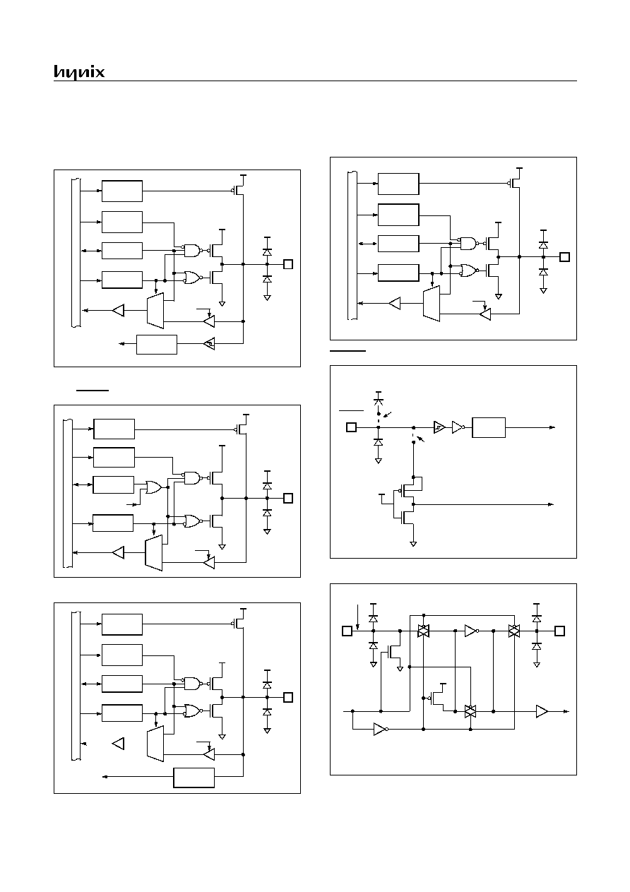
6. PORT STRUCTURES
R00/INT0, R01/INT1, R02/INT2, R03/EC0,
R04/EC2, R05/SCK, R07/S
R30/BUZ, R31/PWM0/T1O, R32/PWM1/T3O,
R34/WDTO, R06
R20/AN0~R27/AN7
R10~R11, R33, R35, R36
RESET
SXIN, SXOUT
Pin
Data Reg.
Dir. Reg.
Noise
Canceller
INT0 ~ INT2
Pull up
Reg.
M U X
RD
V
DD
V
SS
Pull-up Tr.
EC0,EC2
Open Drain
Reg.
Da
ta
B
u
s
SI,SCK
Tr.: Transistor
Reg.: Register
Pin
Data Reg.
Dir. Reg.
Pull up
Reg.
M U X
V
DD
V
SS
Pull-up Tr.
Open Drain
Reg.
BUZ,SO,WDTO
Da
ta
B
u
s
PWM0,PWM1
RD
Pin
Data Reg.
Dir. Reg.
Analog
Switch
AN0 ~ AN 7
P ull up
Reg.
M U X
RD
V
DD
V
SS
Pull-up Tr.
Open Drain
Reg.
Da
ta B
u
s
Pin
Data Reg.
Dir. Reg.
Pull up
Reg.
M U X
RD
V
DD
V
SS
Pull-up Tr.
Open Drain
Reg.
Da
ta
B
u
s
RESET
V
SS
Noise
Canceller
Internal RESET
V
SS
V
DD
High Voltage On(OTP)
V
DD
OTP MCU :disconnected
Mask MCU :connected
OTP MCU :connected
Mask MCU :disconnected
SXOUT
V
SS
Internal
SXIN
Sub clock OFF
(R35)
(R36)
V
DD
System Clock
LCR.7=0
GMS81C7008/7016
10
APR., 2001 Ver 2.01
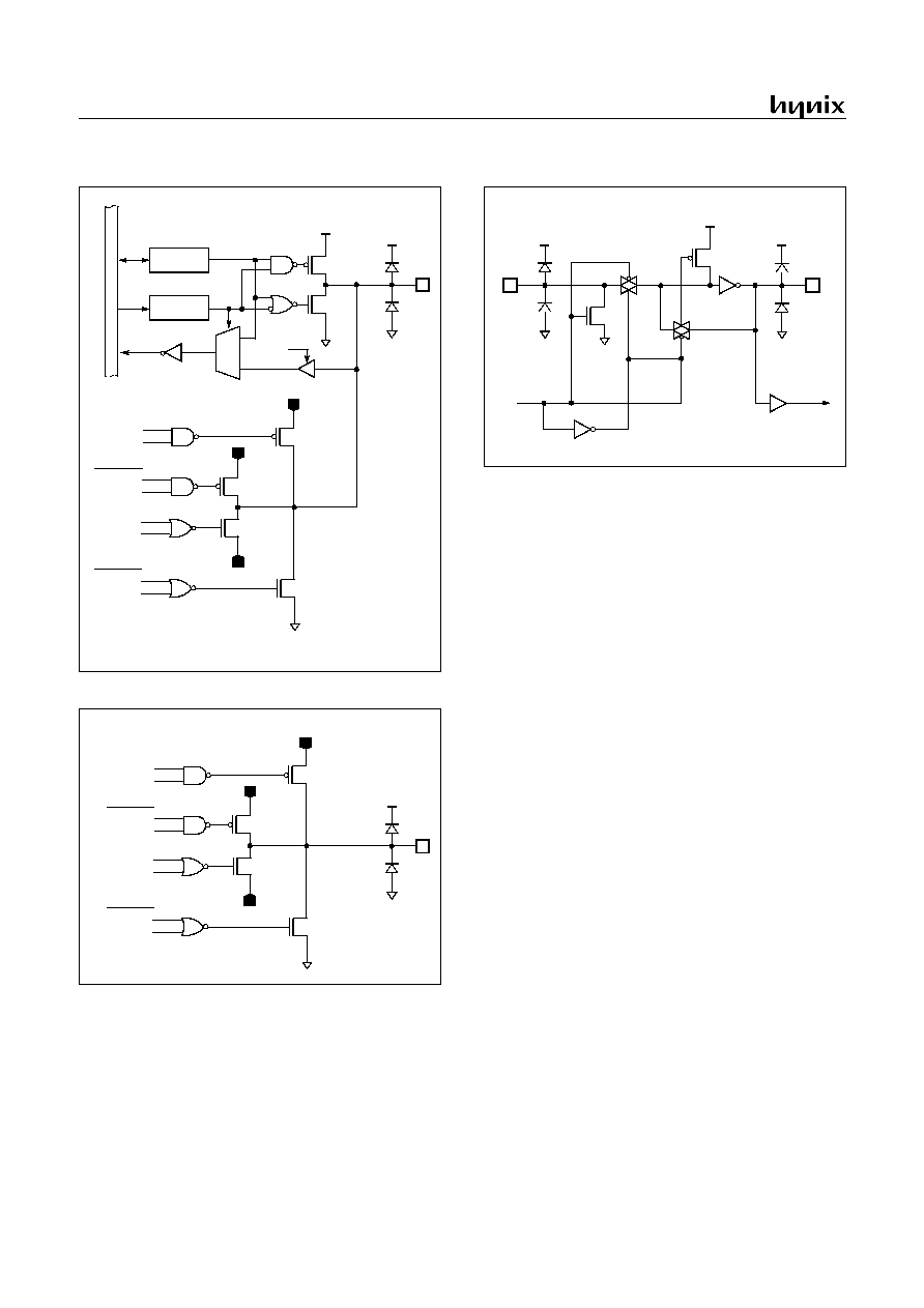
R40~R47, R50~R57, R60~R67 / SEG0~SEG23
COM0~COM3 / SEG24~SEG26
XIN, XOUT
Pin
Data Reg.
Dir. Reg.
M U X
RD
V
DD
V
SS
Da
t
a
Bu
s
VCL2
VCL1
V
SS
VCL0
LCD Data
VCL2 Enable
LCD Data
VCL1 Enable
LCD Data
VCL0 Enable
LCD Data
GND Enable
Pin
VCL2
VCL1
V
SS
VCL0
LCD Data
VCL2 Enable
LCD Data
VCL1 Enable
LCD Data
VCL0 Enable
LCD Data
GND Enable
XOUT
V
DD
V
SS
Main Clock
XIN
STOP & Main
Clock OFF
GMS81C7008/7016
APR., 2001 Ver 2.01
11
7. ELECTRICAL CHARACTERISTICS
7.1 Absolute Maximum Ratings
Supply voltage ........................................... -0.3 to +6.0 V
Storage Temperature ................................-40 to +125
°
C
Voltage on any pin with respect to Ground (V
SS
)
............................................................... -0.3 to V
DD
+0.3
Maximum current out of V
SS
pin ........................100 mA
Maximum current into V
DD
pin ............................80 mA
Maximum current sunk by (I
OL
per I/O Pin) ........20 mA
Maximum output current sourced by (I
OH
per I/O Pin)
...............................................................................15 mA
Maximum current (
I
OL
) .................................... 100 mA
Maximum current (
I
OH
)...................................... 60 mA
Note: Stresses above those listed under "Absolute Maxi-
mum Ratings" may cause permanent damage to the de-
vice. This is a stress rating only and functional operation of
the device at any other conditions above those indicated in
the operational sections of this specification is not implied.
Exposure to absolute maximum rating conditions for ex-
tended periods may affect device reliability.
7.2 Recommended Operating Conditions
7.3 DC Electrical Characteristics
(T
A
=-20~85
°
C, V
DD
=2.7~5.5V)
,
Parameter
Symbol
Condition
Specifications
Unit
Min.
Max.
Supply Voltage
V
DD
f
XIN
=4.19MHz
f
SXIN
=32.768kHz
2.7
5.5
V
Operating Frequency
f
XIN
V
DD
=2.7~5.5V
1
4.5
MHz
Sub Operating Frequency
f
SXIN
V
DD
=2.7~5.5V
30
35
kHz
Operating Temperature
T
OPR
-20
+85
°
C
Parameter
Symbol
Condition
Specifications
Unit
Min.
Typ.
Max.
Input High Voltage
V
IH1
RESET, R0 (except R06)
0.8 V
DD
-
V
DD
V
V
IH2
Other pins
0.7 V
DD
-
V
DD
V
Input Low Voltage
V
IL1
RESET, R0 (except R06)
0
-
0.2 V
DD
V
V
IL2
Other pins
0
-
0.3 V
DD
V
Output High Voltage
V
OH1
R0,R1,R2,R3 I
OH1
=-0.5mA
V
DD
-0.1
-
-
V
V
OH2
SEG, COM I
OH2
=-30
µ
A
-
-
0.4
V
Output Low Voltage
V
OL1
R0,R1,R2,R3 I
OL1
=0.4mA
-
-
0.2
V
V
OL2
SEG, COM I
OL2
=30
µ
A
V
DD
-0.2
-
-
V
Input High
Leakage Current
I
IH1
V
IN
=V
DD
, All input pins except X
IN
, SX
IN
-
-
1
µ
A
I
IH2
V
IN
=V
DD,
X
IN
, SX
IN
-
-
20
µ
A
GMS81C7008/7016
12
APR., 2001 Ver 2.01
Input Low
Leakage Current
I
IL1
V
IN
=0, All input pins except X
IN
, SX
IN
-
-
-1
µ
A
I
IL2
V
IN
=0
,
X
IN
, SX
IN
-
-
-20
µ
A
Pull-up Resistor
1
R
PORT
V
IN
=0V, V
DD
=5.5V, R0, R1, R2
60
160
350
k
LCD Voltage Dividing
Resistor
R
LCD
V
DD
=5.5V
45
65
85
k
Voltage Drop
|V
DD
-COM
n| , n=0~3
V
DC
V
DD
=2.7 ~ 5.5V
-15
µ
A per common pin
-
-
120
mV
Voltage Drop
|V
DD
-SEG
n| , n=0~26
V
DS
V
DD
=2.7 ~ 5.5V
-15
µ
A per segment pin
-
-
120
mV
V
CL2
Output Voltage
V
CL2
V
DD
=2.7 ~ 5.5V, 1/3 bias
BIAS pin and VCL2 pin are shorted
V
DD
-0.3
V
DD
V
DD
+0.3
V
V
CL1
Output Voltage
V
CL1
0.66V
DD
-0.2
0.66V
DD
0.66V
DD
+0.3
V
CL0
Output Voltage
V
CL0
0.33V
DD
-0.3
0.33V
DD
0.33V
DD
+0.3
RC Oscillation Fre-
quency
f
RC
R=60k
, V
DD
= 5V
1
2
3
MHz
Supply Current
1
( ) means at 3V opera-
tion
I
DD1
Main clock operation mode
2
V
DD
=5.5V
±
10%, X
IN
=4MHz, S
XIN
=32kHz
-
2.9
(1.3)
7.0
(3.0)
mA
I
DD2
Sleep mode (Main active)
3
V
DD
=5.5V
±
10%, X
IN
=4MHz, S
XIN
=32kHz
-
0.4
(0.1)
1.7
(1.0)
mA
I
DD3
Stop mode
2
V
DD
=5V
±
10%, X
IN
= 0Hz, S
XIN
=32kH z
2.0
(1.0)
12
(5)
µ
A
I
DD4
Sub clock operation mode
4
V
DD
=5.5V
±
10%, X
IN
=0Hz, S
XIN
=32kHz
-
350
(70)
500
(200)
µ
A
I
DD5
Sleep mode (Sub active)
5
V
DD
=3V
±
10%, X
IN
= 0Hz, S
XIN
=32kH z
-
10
(3)
50
(20)
µ
A
I
DD6
Stop mode
4
V
DD
=5V
±
10%, X
IN
= 0Hz, S
XIN
=0H z
S
XIN
, SXOUT are used as R35, R36.
-
1.0
(0.5)
12
(5)
µ
A
1. Supply current in the following circuits are not included; on-chip pull-up resistors, internal LCD voltage dividing resistors, comparator volt-
age divide resistor, LVD circuit and output port drive currents.
2. This mode set System Clock Mode Register(SCMR) to xxxx0000
B
that is f
XIN
/2
3. This mode set SCMR to xxxx0000
B
(f
XIN
/2) and set SMR to "1".
4. Main-frequency clock stops and sub-frequency clock in not used and set SCMR to xxxx0011
B
.
5. Main-frequency clock stops and sub-frequency clock in not used, set SCMR to xxxx0011
B
and set SMR to "1".
Parameter
Symbol
Condition
Specifications
Unit
Min.
Typ.
Max.
GMS81C7008/7016
APR., 2001 Ver 2.01
13
7.4 A/D Converter Characteristics
(T
A
=25
°
C, V
SS
=0V, V
DD
=5.0V, AV
DD
=5.0V @f
XIN
=4MHz)
7.5 AC Characteristics
(T
A
=-20~+85
°
C, V
DD
=5V
±
10%
,
V
SS
=0V)
Parameter
Symbol
Test Condition
Specifications
Unit
Min.
Typ.
1
1. Data in "Typ" column is at 25
°
C unless otherwise stated. These parameters are for design guidance only and are not tested.
Max.
Analog Input Voltage Range
V
AIN
V
DD
=AV
DD
=5.0V
V
SS
-0.3
-
AV
DD
+0.3
V
Non-linearity Error
N
NLE
-
±
1.0
±1.5
LSB
Differential Non-linearity Error
N
DNLE
-
±
1.0
±1.5
LSB
Zero Offset Error
N
ZOE
-
±
0.5
±1.5
LSB
Full Scale Error
N
FSE
-
±
0.25
±0.5
LSB
Gain Error
N
GE
-
±
1.0
±1.5
LSB
Overall Accuracy
N
ACC
-
±
1.0
±1.5
LSB
AV
DD
Input Current
I
REF
-
-
200
µ
A
Conversion Time
T
CONV
-
-
20
µ
s
Analog Power Supply Input Range
AV
DD
V
DD
=5.0V
V
DD
=3.0V
3.0
2.7
-
V
DD
V
Parameter
Symbol
Pins
Specifications
Unit
Min.
Typ.
Max.
Operating Frequency
f
MAIN
X
IN
0.455
-
4.2
MHz
f
SUB
SX
IN
30
32.768
35
kHz
External Clock Pulse Width
t
MCPW
X
IN
80
-
-
nS
t
SCPW
SX
IN
14.7
-
-
µ
S
External Clock Transition Time
t
MRCP,
t
MFCP
X
IN
-
-
20
nS
t
SRCP,
t
SFCP
SX
IN
-
-
3
µ
S
Main oscillation Stabilizing
Time
t
MST
X
IN
, X
OUT
at 4MHz
-
-
20
mS
Sub oscillation Stabilizing Time
t
SST
SX
IN
, SX
OUT
-
0.5
1
S
Interrupt Pulse Width
t
IW
INT0, INT1, INT2
2
-
-
t
SYS
1
RESET Input Width
t
RST
RESET
8
-
-
t
SYS
1
Event Counter Input Pulse
Width
t
ECW
EC0, EC2
2
-
-
t
SYS
1
1. t
SYS
is one of 2/f
MAIN
or 8/f
MAIN
or 16/f
MAIN
or 64/f
MAIN
in the main clock operation mode,
t
SYS
is one of 2/f
SUB
or 8/f
SUB
or 16/f
SUB
or 64/f
SUB
in the sub clock operation mode.
GMS81C7008/7016
14
APR., 2001 Ver 2.01
Figure 7-1 Timing Chart
t
MRCP
t
MFCP
X
IN
INT0, INT1
INT2
0.5V
V
DD
-0.5V
0.2V
DD
0.8V
DD
0.2V
DD
RESET
0.2V
DD
0.8V
DD
EC0, EC2
t
IW
t
IW
t
RST
t
ECW
t
ECW
1/f
MAIN
t
MCPW
t
MCPW
t
SRCP
t
SFCP
SX
IN
0.5V
V
DD
-0.5V
1/f
SUB
t
SCPW
t
SCPW
t
SYS
GMS81C7008/7016
APR., 2001 Ver 2.01
15
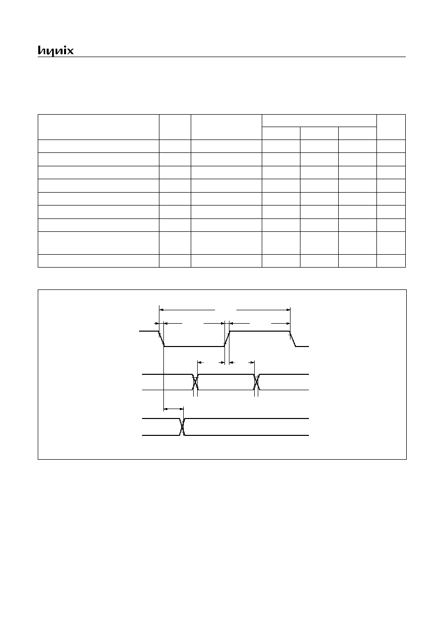
7.6 Serial Interface Timing Characteristics
(T
A
=-20~+85
°
C, V
DD
=2.7~5.5V, V
SS
=0V, f
XIN
=4MHz)
Figure 7-2 Serial I/O Timing Chart
Parameter
Symbol
Pins
Specifications
Unit
Min.
Typ.
Max.
Serial Input Clock Pulse
t
SCYC
SCK
2t
SYS
+200
-
8
ns
Serial Input Clock Pulse Width
t
SCKW
SCK
t
SYS
+70
-
8
ns
SIN Input Setup Time (External SCK)
t
SUS
SIN
100
-
-
ns
SIN Input Setup Time (Internal SCK)
t
SUS
SIN
200
-
-
ns
SIN Input Hold Time
t
HS
SIN
t
SYS
+70
-
-
ns
Serial Output Clock Cycle Time
t
SCYC
SCK
4t
SYS
-
16t
SYS
ns
Serial Output Clock Pulse Width
t
SCKW
SCK
t
SYS
-30
-
-
ns
Serial Output Clock Pulse Transition
Time
t
FSCK
t
RSCK
SCK
-
-
30
ns
Serial Output Delay Time
s
OUT
SO
-
-
100
ns
SCLK
SIN
0.2V
DD
SOUT
0.2V
DD
0.8V
DD
t
SCYC
t
SCKW
t
SCKW
t
RSCK
t
FSCK
0.8V
DD
t
SUS
t
HS
t
DS
0.2V
DD
0.8V
DD
GMS81C7008/7016
16
APR., 2001 Ver 2.01
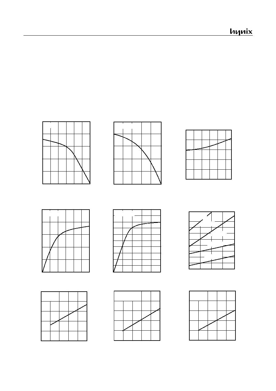
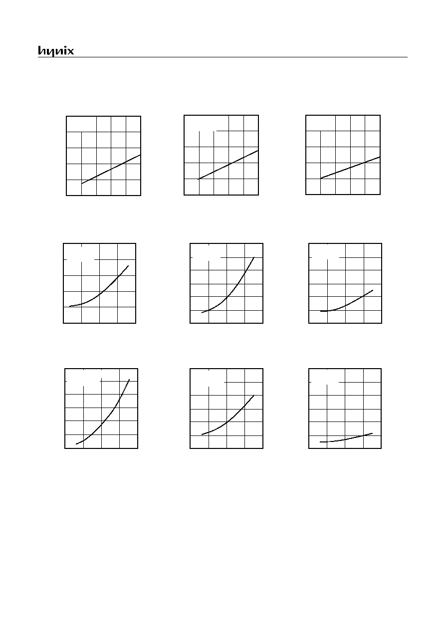
7.7 Typical Characteristics
This graphs and tables provided in this section are for de-
sign guidance only and are not tested or guaranteed.
In some graphs or tables the data presented are out-
side specified operating range (e.g. outside specified
V
DD
range). This is for information only and devices
are guaranteed to operate properly only within the
specified range.
The data presented in this section is a statistical summary
of data collected on units from different lots over a period
of time. "Typical" represents the mean of the distribution
while "max" or "min" represents (mean + 3
) and (mean
-
3
) respectively where
is standard deviation
I
OL
-
-
-
-
V
OL
, V
DD
=5.5V
40
30
20
10
0
(mA)
I
OL
V
OL
(V)
I
OL
-
-
-
-
V
OL
, V
DD
=3.0V
(mA)
I
OL
0.5
1.0 1.5
2.0
2.5
V
OL
(V)
I
OH
-
-
-
-
V
OH
, V
DD
=5.0V
-20
-15
-10
-5
0
(mA)
I
OH
1
2
3
4
5
V
OH
(V)
I
OH
-
-
-
-
V
OH
, V
DD
=3.0V
-8
-6
-4
-2
0
(mA)
I
OH
0.5
1.0 1.5
2.0
2.5
V
OH
(V)
Ta=25
°
C
R0,R1,R2,R3 pin
200
100
0
(k
)
-20
0
40
80
Ta
(
°
C)
R
1
2
3
4
5
f
XIN
=4MHz
V
DD
-
-
-
-
V
IH1
4
3
2
1
0
(V)
V
IH1
2
3
4
5
6
V
DD
(V)
V
DD
-
-
-
-
V
IH2
4
3
2
1
0
(V)
V
IH2
2
3
4
5
6
V
DD
(V)
Ta=25
°
C
f
XIN
=4MHz
Ta=25
°
C
1
R0 (except R06)
R1~R6 pin
20
15
10
5
(include R06)
f
XIN
=4MHz
V
DD
-
-
-
-
V
IH3
4
3
2
1
0
(V)
V
IH1
2
3
4
5
6
V
DD
(V)
Ta=25
°
C
1
X
IN
, SX
IN
R = 6.2k
4
3
2
1
0
(MHz)
f
XIN
2
3
4
5
6
V
DD
(V)
Ta=25
°
C
R = 20k
R = 180k
R = 60k
f
XIN
-
-
-
-
V
DD
Ta=25
°
C
Ta=25
°
C
Ta=25
°
C
R
PU
-
-
-
-
T
a
, V
DD
=5.0V
GMS81C7008/7016
APR., 2001 Ver 2.01
17
I
STOP
(
(
(
(
I
DD6
)
-
-
-
-
V
DD
STOP Mode
I
DD1
-
-
-
-
V
DD
4
3
2
1
0
(mA)
I
DD
6
V
DD
(V)
Normal Operation (Main opr.)
I
DD4
-
-
-
-
V
DD
400
300
200
100
0
(
µ
A)
I
DD
2
3
4
5
6
V
DD
(V)
Normal Mode (Sub opr.)
I
SLEEP
(I
DD5
)
-
-
-
-
V
DD
SLEEP Mode (Sub opr.)
I
SLEEP
(I
DD2
)
-
-
-
-
V
DD
f
XIN
=4MHz
V
DD
-
-
-
-
V
IL1
4
3
2
1
0
(V)
V
IH1
2
3
4
5
6
V
DD
(V)
V
DD
-
-
-
-
V
IL2
4
3
2
1
0
(V)
V
IH2
2
3
4
5
6
V
DD
(V)
Ta=25
°
C
f
XIN
=4MHz
Ta=25
°
C
1
R0 (except R06)
R1~R6 pin
(include R06)
f
XIN
=4MHz
V
DD
-
-
-
-
V
IL3
4
3
2
1
0
(V)
V
IH1
2
3
4
5
6
V
DD
(V)
Ta=25
°
C
1
X
IN
, SX
IN
2
3
4
5
SLEEP Mode (Main opr.)
f
SXIN
=32kHz
Ta=25
°
C
400
300
200
100
0
(
µ
A)
I
DD
2
3
4
5
6
V
DD
(V)
12
9
6
3
0
(
µ
A)
I
DD
2
3
4
5
6
V
DD
(V)
f
SXIN
=32kHz
Ta=25
°
C
I
STOP
(I
DD3
)
-
-
-
-
V
DD
STOP Mode
4
3
2
1
0
(
µ
A)
I
DD
2
3
4
5
6
V
DD
(V)
f
XIN
=0Hz
Ta=25
°
C
f
XIN
=4MHz
Ta=25
°
C
f
XIN
=4MHz
Ta=25
°
C
4
3
2
1
0
(
µ
A)
I
DD
2
3
4
5
6
V
DD
(V)
f
SXIN
=0Hz
Ta=25
°
C
GMS81C7008/7016
18
APR., 2001 Ver 2.01
8. MEMORY ORGANIZATION
The GMS81C7008/16 has separate address spaces for Program
memory and Data Memory. Program memory can only be read,
not written to. It can be up to 8K/16K bytes of Program memory.
Data memory can be read and written to up to 448 bytes including
the stack area and the LCD display RAM area.
8.1 Registers
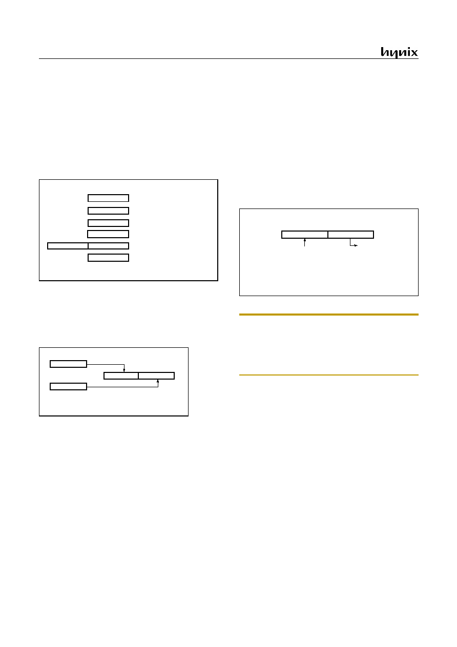
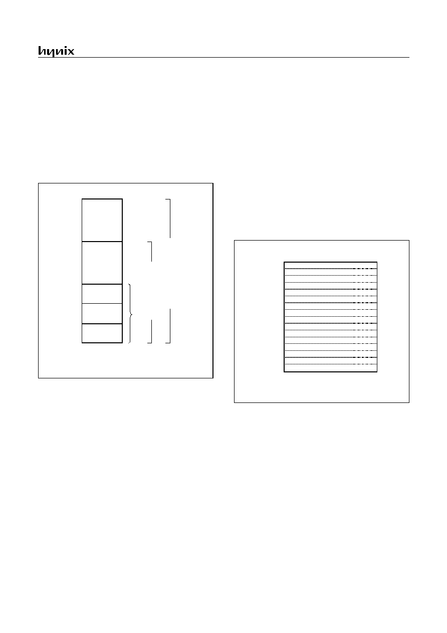
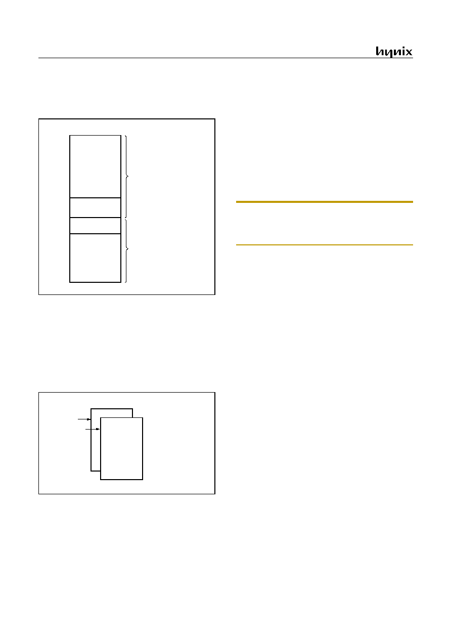
This device has six registers that are the Program Counter (PC),
a Accumulator (A), two index registers (X, Y), the Stack Pointer
(SP), and the Program Status Word (PSW). The Program Counter
consists of 16-bit register.
Figure 8-1 Configuration of Registers
Accumulator: The Accumulator is the 8-bit general purpose reg-
ister, used for data operation such as transfer, temporary saving,
and conditional judgement, etc.
The Accumulator can be used as a 16-bit register with Y Register
as shown below.
Figure 8-2 Configuration of YA 16-bit Register
X, Y Registers: In the addressing mode which uses these index
registers, the register contents are added to the specified address,
which becomes the actual address. These modes are extremely ef-
fective for referencing subroutine tables and memory tables. The
index registers also have increment, decrement, comparison and
data transfer functions, and they can be used as simple accumula-
tors.
Stack Pointer: The Stack Pointer is an 8-bit register used for oc-
currence interrupts and calling out subroutines. Stack Pointer
identifies the location in the stack to be access (save or restore).
Generally, SP is automatically updated when a subroutine call is
executed or an interrupt is accepted. However, if it is used in ex-
cess of the stack area permitted by the data memory allocating
configuration, the user-processed data may be lost.
The stack can be located at any position within 011B
H
to 01FF
H
of the internal data memory. The SP is not initialized by hard-
ware, requiring to write the initial value (the location with which
the use of the stack starts) by using the initialization routine. Nor-
mally, the initial value of "FF
H
" is used.
Note: The Stack Pointer must be initialized by software be-
cause its value is undefined after RESET.
Example: To initialize the SP
LDX
#0FFH
TXSP
; SP
FFH
Program Counter: The Program Counter is a 16-bit wide which
consists of two 8-bit registers, PCH and PCL. This counter indi-
cates the address of the next instruction to be executed. In reset
state, the program counter has reset routine address (PC
H
:0FF
H
,
PC
L
:0FE
H
).
Program Status Word: The Program Status Word (PSW) con-
tains several bits that reflect the current state of the CPU. The
PSW is described in Figure 8-3. It contains the Negative flag, the
Overflow flag, the Break flag the Half Carry (for BCD opera-
tion), the Interrupt enable flag, the Zero flag, and the Carry flag.
[Carry flag C]
This flag stores any carry or not borrow from the ALU of CPU
after an arithmetic operation and is also changed by the Shift In-
struction or Rotate Instruction.
[Zero flag Z]
This flag is set when the result of an arithmetic operation or data
transfer is "0" and is cleared by any other result.
ACCUMULATOR
X REGISTER
Y REGISTER
STACK POINTER
PROGRAM COUNTER
PROGRAM STATUS
WORD
X
A
SP
Y
PCL
PSW
PCH
Two 8-bit Registers can be used as a "YA" 16-bit Register
Y
A
Y
A
SP
01
H
Stack Area (100
H
~ 1FF
H
)
Bit 15
Bit 0
8 7
Hardware fixed
00
H
~FF
H
LCD display RAM area is located in 100
H
~11A
H
,
SP (Stack Pointer) could be in 00
H
~FF
H
.
User must have concerning that Stack data does not
cross over LCD RAM area.
GMS81C7008/7016
APR., 2001 Ver 2.01
19
Figure 8-3 PSW (Program Status Word) Register
[Interrupt disable flag I]
This flag enables/disables all interrupts except interrupt caused
by Reset or software BRK instruction. All interrupts are disabled
when cleared to "0". This flag immediately becomes "0" when an
interrupt is served. It is set by the EI instruction and cleared by
the DI instruction.
[Half carry flag H]
After operation, this is set when there is a carry from bit 3 of ALU
or there is no borrow from bit 4 of ALU. This bit can not be set
or cleared except CLRV instruction with Overflow flag (V).
[Break flag B]
This flag is set by software BRK instruction to distinguish BRK
from TCALL instruction with the same vector address.
[Direct page flag G]
This flag assigns RAM page for direct addressing mode. In the di-
rect addressing mode, addressing area is from zero page 00
H
to
0FF
H
when this flag is "0". If it is set to "1", addressing area is
assigned by RPR register (address 0F3
H
). It is set by SETG in-
struction and cleared by CLRG.
When content of RPR is above 2, malfunction will be occurred.
[Overflow flag V]
This flag is set to "1" when an overflow occurs as the result of an
arithmetic operation involving signs. An overflow occurs when
the result of an addition or subtraction exceeds +127(7F
H
) or -
128(80
H
). The CLRV instruction clears the overflow flag. There
is no set instruction. When the BIT instruction is executed, bit 6
of memory is copied to this flag.
[Negative flag N]
This flag is set to match the sign bit (bit 7) status of the result of
a data or arithmetic operation. When the BIT instruction is exe-
cuted, bit 7 of memory is copied to this flag.
N
NEGATIVE FLAG
V
G
B
H
I
Z
C
MSB
LSB
RESET VALUE: 00
H
PSW
OVERFLOW FLAG
BRK FLAG
CARRY FLAG RECEIVES
ZERO FLAG
INTERRUPT ENABLE FLAG
CARRY OUT
HALF CARRY FLAG RECEIVES
CARRY OUT FROM BIT 1 OF
ADDITION OPERLANDS
SELECT DIRECT PAGE
when G=1, page is selected to "page 1"
RAM Page
Instruction
Bit1 of
RPR
Bit0 of
RPR
0 page
CLRG
X
X
0 page
SETG
0
0
1 page
SETG
0
1
Reserved
SETG
1
0
Reserved
SETG
1
1
GMS81C7008/7016
20
APR., 2001 Ver 2.01
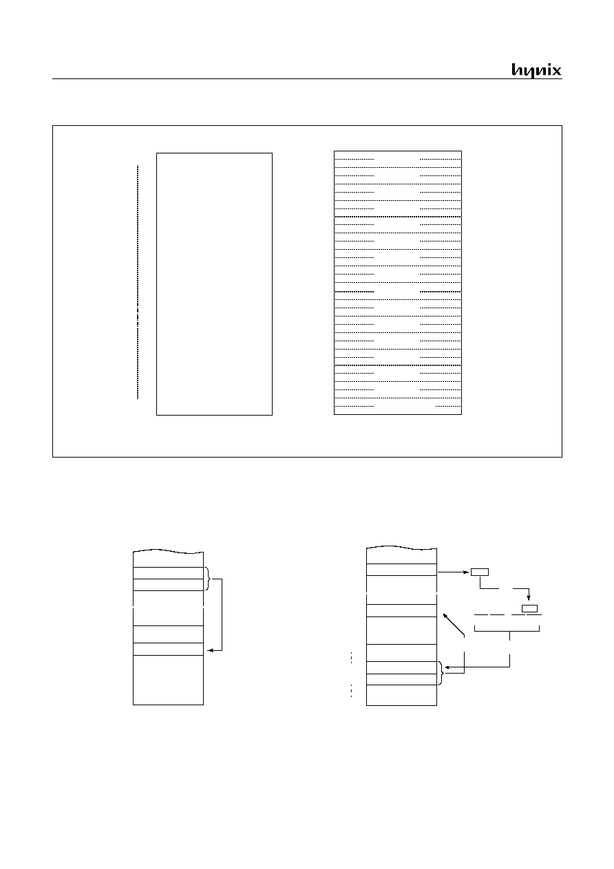
Figure 8-4 Stack Operation
At execution of
a CALL/TCALL/PCALL
PCL
PCH
01FC
SP after
execution
SP before
execution
01FD
01FD
01FE
01FF
01FF
Push
down
At acceptance
of interrupt
PCL
PCH
01FC
01FC
01FD
01FE
01FF
01FF
Push
down
PSW
At execution
of RET instruction
PCL
PCH
01FC
01FF
01FD
01FE
01FF
01FD
Pop
up
At execution
of RET instruction
PCL
PCH
01FC
01FF
01FE
01FE
01FF
01FC
Pop
up
PSW
0100H
01FFH
Stack
depth
At execution
of PUSH instruction
A
01FC
01FE
01FD
01FE
01FF
01FF
Push
down
SP after
execution
SP before
execution
PUSH A (X,Y,PSW)
At execution
of POP instruction
A
01FC
01FF
01FD
01FE
01FF
01FE
Pop
up
POP A (X,Y,PSW)
GMS81C7008/7016
APR., 2001 Ver 2.01
21
8.2 Program Memory
A 16-bit program counter is capable of addressing up to 64K
bytes, but this device has 8K/16K bytes program memory space
only physically implemented. Accessing a location above FFFF
H
will cause a wrap-around to 0000
H
.
Figure 8-5, shows a map of Program Memory. After reset, the
CPU begins execution from reset vector which is stored in ad-
dress FFFE
H
and FFFF
H
as shown in Figure 8-6.
As shown in Figure 8-5, each area is assigned a fixed location in
Program Memory. Program Memory area contains the user pro-
gram.
Figure 8-5 Program Memory Map
Page Call (PCALL) area contains subroutine program to reduce
program byte length by using 2 bytes PCALL instead of 3 bytes
CALL instruction. If it is frequently called, it is more useful to
save program byte length.
Table Call (TCALL) causes the CPU to jump to each TCALL ad-
dress, where it commences the execution of the service routine.
The Table Call service area spaces 2-byte for every TCALL:
0FFC0
H
for TCALL15, 0FFC2
H
for TCALL14, etc., as shown in
Figure 8-7.
Example: Usage of TCALL
The interrupt causes the CPU to jump to specific location, where
it commences the execution of the service routine. The External
interrupt 0, for example, is assigned to location 0FFFA
H
. The in-
terrupt service locations spaces 2-byte interval: 0FFF8
H
and
0FFF9
H
for External Interrupt 1, 0FFFA
H
and 0FFFB
H
for Exter-
nal Interrupt 0, etc.
Any area from 0FF00
H
to 0FFFF
H
, if it is not going to be used,
its service location is available as general purpose Program Mem-
ory.
Figure 8-6 Interrupt Vector Area
Interrupt
Vector Area
C000
H
FEFF
H
FF00
H
FFC0
H
FFDF
H
FFE0
H
FFFF
H
P
C
A
LL are
a
E000
H
TCALL area
G
M
S
8
1
C
70
08
8K
R
O
M
GM
S
8
1
C
701
6
1
6
K RO
M
0FFE0
H
E2
Address
Vector Area Memory
E4
E6
E8
EA
EC
EE
F0
F2
F4
F6
F8
FA
FC
FE
Timer/Counter 3
Timer/Counter 2
Watch Timer
A/D Converter
-
External Interrupt 0
Timer/Counter 1
Basic Interval Timer
Key Scan
RESET
Watchdog Timer
Serial Peripheral Interface
"-" means reserved area.
NOTE:
External Interrupt 2
External Interrupt 1
Timer/Counter 0
-
-
GMS81C7008/7016
22
APR., 2001 Ver 2.01
Figure 8-7 PCALL and TCALL Memory Area
PCALL
rel
4F35
PCALL 35H
TCALL
n
4A
TCALL
4
0FFC0
H
C1
Address
Program Memory
C2
C3
C4
C5
C6
C7
C8
0FF00
H
Address
PCALL Area Memory
0FFFF
H
PCALL Area
(256 Bytes)
* means that the BRK software interrupt is using
same address with TCALL0.
NOTE:
TCALL 15
TCALL 14
TCALL 13
TCALL 12
TCALL 11
TCALL 10
TCALL 9
TCALL 8
TCALL 7
TCALL 6
TCALL 5
TCALL 4
TCALL 3
TCALL 2
TCALL 1
TCALL 0 / BRK *
C9
CA
CB
CC
CD
CE
CF
D0
D1
D2
D3
D4
D5
D6
D7
D8
D9
DA
DB
DC
DD
DE
DF
4F
~
~
~
~
NEXT
35
0FF35
H
0FF00
H
0FFFF
H
11111111 11010110
01001010
PC:
FH
FH
DH 6H
4A
~
~
~
~
25
0FFD6
H
0FF00
H
0FFFF
H
D1
NEXT
0FFD7
H
0D125
H
Reverse
1
2
3

GMS81C7008/7016
APR., 2001 Ver 2.01
23
Example: The usage software example of Vector address for GMS81C7016.
ORG
0FFE0H
DW
TIMER3
; Timer-3
DW
TIMER2
; Timer-2
DW
WATCH_TIMER
; Watch Timer
DW
ADC
; ADC
DW
SIO
; Serial Interface
DW
NOT_USED
; -
DW
NOT_USED
; -
DW
INT2
; Int.2
DW
TIMER1
; Timer-1
DW
TIMER0
; Timer-0
DW
INT1
; Int.1
DW
INT0
; Int.0
DW
WD_TIMER
; Watchdog Timer
DW
BIT_TIMER
; Basic Interval Timer
DW
KEYSCAN
; Key Scan Timer
DW
RESET
; Reset
ORG
0C000H
; in case of 16K ROM Start address
;
ORG
0E000H
; in case of 8K ROM Start address
;*******************************************
;
MAIN PROGRAM *
;*******************************************
;
RESET:
LDM
SCMR,#0
;When main clock mode
DI
;Disable All Interrupts
LDM
WDTR,#0
;Disable Watch Dog Timer
LDM
RPR,#1
CLRG
LDX
#0
RAM_CLR: LDA
#0
;RAM Clear(!0000H ~ !00BFH)
STA
{X}+
CMPX
#0C0H
BNE
RAM_CLR
SETG
LDX
#0
RAM_CLR1:
LDA
#0
STA
{X}+
CMPX
#1BH
;DISPLAY RAM Clear(!0100H ~ !011AH)
BNE
RAM_CLR1
CLRG
;
LDX
#0FFH
;Stack Pointer Initialize
TXSP
;
LDM
R0, #0
;Normal Port 0
LDM
R0DD,#82H
;Normal Port Direction
LDM
R0PU,#0
;Normal Pull Up
:
:
:
LDM
TDR0,#250
;8us x 250 = 2000us
LDM
TM0,#0000_1111B
;Start Timer0, 8us at 4MHz
LDM
IRQH,#0
LDM
IRQL,#0
LDM
IENH,#0000_1110B
;Enable INT0, INT1, Timer0
LDM
IENL,#0
LDM
IEDS,#15H
;Select falling edge detect on INT pin
LDM
PMR,#3H
;Set external interrupt pin(INT0, INT1)
EI
;Enable master interrupt
GMS81C7008/7016
24
APR., 2001 Ver 2.01
8.3 Data Memory
Figure 8-8 shows the internal Data Memory space available. Data
Memory is divided into four groups, a user RAM, control regis-
ters, Stack, and LCD memory.
Figure 8-8 Data Memory Map
User Memory
The both GMS81C7008/16 has 448
×
8 bits for the user memory
(RAM).
There are two page internal RAM. Page is selected by G-flag and
RAM page selection register RPR. When G-flag is cleared to "0",
always page 0 is selected regardless of RPR value. If G-flag is set
to "1", page will be selected according to RPR value.
Figure 8-9 RAM page configuration
Control Registers
The control registers are used by the CPU and Peripheral function
blocks for controlling the desired operation of the device. There-
fore these registers contain control and status bits for the interrupt
system, the timer/ counters, analog to digital converters and I/O
ports. The control registers are in address range of 0C0
H
to 0FF
H
.
Note that unoccupied addresses may not be implemented on the
chip. Read accesses to these addresses will in general return ran-
dom data, and write accesses will have an indeterminate effect.
More detailed informations of each register are explained in each
peripheral section.
Note: Write only registers can not be accessed by bit ma-
nipulation instruction (SET1, CLR1). Do not use read-mod-
ify-write instruction. Use byte manipulation instruction, for
example "LDM".
Example; To write at CKCTLR
LDM
CKCTLR,#09H
;Divide ratio(
÷
16)
Stack Area
The stack provides the area where the return address is saved be-
fore a jump is performed during the processing routine at the ex-
ecution of a subroutine call instruction or the acceptance of an
interrupt.
When returning from the processing routine, executing the sub-
routine return instruction [RET] restores the contents of the pro-
gram counter from the stack; executing the interrupt return
instruction [RETI] restores the contents of the program counter
and flags.
The save/restore locations in the stack are determined by the
stack pointed (SP). The SP is automatically decreased after the
saving, and increased before the restoring. This means the value
of the SP indicates the stack location number for the next save.
Refer to Figure 8-4 on page 20.
User Memory
Control
Registers
or Stack Area
0000
H
00BF
H
00C0
H
00FF
H
0100
H
01FF
H
PAGE0
User Memory
PAGE1
LCD display RAM
(27 Nibbles)
011A
H
011B
H
(192 Bytes)
(229 Bytes)
Page 0
Page 0: 00~FF
H
Page 1
Page 1: 100~1FF
H
RPR=1, G=1
G=0
GMS81C7008/7016
APR., 2001 Ver 2.01
25
8.4 List of Control Registers
Address
Register Name
Symbol
R/W
Initial Value
Page
7 6 5 4 3 2 1 0
00C0
R0 port data register
R0
R/W
0 0 0 0 0 0 0 0
page 33
00C1
R1 port data register
R1
R/W
- - - - - - 0 0
page 33
00C2
R2 port data register
R2
R/W
0 0 0 0 0 0 0 0
page 33
00C3
R3 port data register
R3
R/W
- 0 0 0 0 0 0 0
page 33
00C4
R4 port data register
R4
R/W
0 0 0 0 0 0 0 0
page 34
00C5
R5 port data register
R5
R/W
0 0 0 0 0 0 0 0
page 34
00C6
R6 port data register
R6
R/W
0 0 0 0 0 0 0 0
page 35
00C8
R0 port I/O direction register
R0DD
W
0 0 0 0 0 0 0 0
page 35
00C9
R1 port I/O direction register
R1DD
W
- - - - - - 0 0
page 36
00CA
R2 port I/O direction register
R2DD
W
0 0 0 0 0 0 0 0
page 36
00CB
R3 port I/O direction register
R3DD
W
- 0 0 0 0 0 0 0
page 35
00CC
R4 port I/O direction register
R4DD
W
0 0 0 0 0 0 0 0
page 36
00CD
R5 port I/O direction register
R5DD
W
0 0 0 0 0 0 0 0
page 36
00CE
R6 port I/O direction register
R6DD
W
0 0 0 0 0 0 0 0
page 36
00D0
R0 port pull-up register
R0PU
W
0 0 0 0 0 0 0 0
page 33
00D1
R1 port pull-up register
R1PU
W
- - - - - - 0 0
page 33
00D2
R2 port pull-up register
R2PU
W
0 0 0 0 0 0 0 0
page 33
00D3
R3 port pull-up register
R3PU
W
- 0 0 0 0 0 0 0
page 33
00D4
R0 port open drain control register
R0CR
W
0 0 0 0 0 0 0 0
page 33
00D5
R1 port open drain control register
R1CR
W
- - - - - - 0 0
page 33
00D6
R2 port open drain control register
R2CR
W
0 0 0 0 0 0 0 0
page 33
00D7
R3 port open drain control register
R3CR
W
- 0 0 0 0 0 0 0
page 33
00D8
Ext. interrupt edge selection register
IEDS
R/W
- - 0 0 0 0 0 0
page 69
00D9
Port mode register
PMR
R/W
0 0 0 0 0 0 0 0 page 62, page 69
00DA
Interrupt enable lower byte register
IENL
R/W
0 - - 0 0 0 0 0
page 65
00DB
Interrupt enable upper byte register
IENH
R/W
- 0 0 0 0 0 0 0
page 65
00DC
Interrupt request flag lower byte register
IRQL
R/W
0 - - 0 0 0 0 0
page 64
00DD
Interrupt request flag upper byte register
IRQH
R/W
- 0 0 0 0 0 0 0
page 64
00DE
Sleep mode register
SMR
W
- - - - - - - 0
page 81
00DF
Watch dog timer register
WDTR
R/W
- - 0 1 0 0 1 0
page 79
00E0
Timer0 mode register
TM0
R/W
- - 0 0 0 0 0 0
page 45
00E1
Timer0 counter register
T0
R
0 0 0 0 0 0 0 0
page 45
Timer0 data register
TDR0
W
1 1 1 1 1 1 1 1
page 45
Timer0 input capture register
CDR0
R
0 0 0 0 0 0 0 0
page 45
00E2
Timer1 mode register
TM1
R/W
0 0 0 0 0 0 0 0
page 45
Table 8-1 Control Registers
GMS81C7008/7016
26
APR., 2001 Ver 2.01
00E3
Timer1 data register
TDR1
W
1 1 1 1 1 1 1 1
page 45
PWM0 pulse period register
T1PPR
W
1 1 1 1 1 1 1 1
page 54
00E4
Timer1 counter register
T1
R
0 0 0 0 0 0 0 0
page 45
Timer1 input capture register
CDR1
R
0 0 0 0 0 0 0 0
page 45
Timer1 pulse duty register
T1PDR
R/W
0 0 0 0 0 0 0 0
page 54
00E5
PWM0 high register
PWM0HR
W
- - - - 0 0 0 0
page 54
00E6
Timer2 mode register
TM2
R/W
- - 0 0 0 0 0 0
page 46
00E7
Timer2 counter register
T2
R
0 0 0 0 0 0 0 0
page 46
Timer2 data register
TDR2
W
1 1 1 1 1 1 1 1
page 46
Timer2 input capture register
CDR2
R
0 0 0 0 0 0 0 0
page 46
00E8
Timer3 mode register
TM3
R/W
0 0 0 0 0 0 0 0
page 46
00E9
Timer3 data register
TDR3
W
1 1 1 1 1 1 1 1
page 46
PWM1 pulse period register
T3PPR
W
1 1 1 1 1 1 1 1
page 54
00EA
Timer3 counter register
T3
R
0 0 0 0 0 0 0 0
page 46
Timer3 input capture register
CDR3
R
0 0 0 0 0 0 0 0
page 46
Timer3 pulse duty register
T3PDR
R/W
0 0 0 0 0 0 0 0
page 46
00EB
PWM1 high register
PWM1HR
W
- - - - 0 0 0 0
page 54
00EC
A/D converter mode register
ADCM
R/W
- 0 0 0 0 0 0 1
page 58
00ED
A/D converter data register
ADR
R
Undefined
page 58
00EF
Watch timer mode register
WTMR
R/W
- 0 - - 0 0 0 0
page 79
00F0
Key scan port mode register
KSMR
R/W
- - - - - - 0 0
page 69
00F1
LCD control register
LCR
R/W
0 0 0 0 0 0 0 0
page 71
00F2
LCD port mode register high
LPMR
R/W
- - 0 0 0 0 0 0
page 71
00F3
RAM paging register
RPR
R/W
- - - - - - 0 0 page 24, page 71
00F4
Basic interval timer register
BITR
R
0 0 0 0 0 0 0 0
page 43
Clock control register
CKCTLR
W
- - - 0 0 1 1 1
page 43
00F5
System clock mode register
SCMR
R/W
0 0 0 0 0 0 0 0
page 38
00FB
LVD register
LVDR
R/W
0 0 0 0 0 - - -
page 87
00FD
Buzzer data register
BUR
W
0 0 0 0 0 0 0 0
page 62
00FE
Serial I/O mode register
SIOM
R/W
0 0 0 0 0 0 0 1
page 59
00FF
Serial I/O Data register
SIOR
R/W
Undefined
page 59
Address
Register Name
Symbol
R/W
Initial Value
Page
7 6 5 4 3 2 1 0
Table 8-1 Control Registers
Registers are controlled by byte manipulation instruction such as LDM etc., do not use bit manipulation
W
Registers are controlled by both bit and byte manipulation instruction.
R/W
instruction such as SET1, CLR1 etc. If bit manipulation instruction is used on these registers,
content of other seven bits are may varied to unwanted value.
- : this bit location is reserved.
GMS81C7008/7016
APR., 2001 Ver 2.01
27
Three registers are mapped on same address.
Two registers are mapped on same address.
Address
Timer/Counter mode
Capture mode
PWM mode
E1
H
T0 [R], TDR0 [W]
CDR0 [R], TDR0 [W]
-
E3
H
TDR1 [W]
TDR1 [W]
T1PPR [W]
E4
H
T1 [R]
CDR1 [R]
T1PDR [R/W]
E7
H
T2 [R], TDR2 [W]
CDR2 [R], TDR2 [W]
-
E9
H
TDR3 [W]
TDR3 [W]
T3PPR [W]
EA
H
T3 [R]
CDR3 [R]
T3PDR [R/W]
Address
Basic Interval Timer
F4
H
BITR [R], CKCTLR [W]
GMS81C7008/7016
28
APR., 2001 Ver 2.01
8.5 Addressing Mode
The GMS800 series MCU uses six addressing modes;
· Register addressing
· Immediate addressing
· Direct page addressing
· Absolute addressing
· Indexed addressing
· Register-indirect addressing
(1) Register Addressing
Register addressing accesses the A, X, Y, C and PSW.
(2) Immediate Addressing
#imm
In this mode, second byte (operand) is accessed as a data imme-
diately.
Example:
0435
ADC
#35H
When G-flag is 1, then RAM address is defined by 16-bit address
which is composed of 8-bit RAM paging register (RPR) and 8-bit
immediate data.
Example: G=1, RPR=01
E45535
LDM
35H,#55H
(3) Direct Page Addressing
dp
In this mode, a address is specified within direct page.
Example; G=0
C535
LDA
35H
;A
RAM[35H]
35
A+35H+C
A
04
MEMORY
E4
0F100H
data
55H
~
~
~
~
data
0135H
35
0F102H
55
0F101H
data
35
35H
0E551H
data
A
~
~
~
~
C5
0E550H
GMS81C7008/7016
APR., 2001 Ver 2.01
29
(4) Absolute Addressing
!abs
Absolute addressing sets corresponding memory data to Data, i.e.
second byte (Operand I) of command becomes lower level ad-
dress and third byte (Operand II) becomes upper level address.
With 3 bytes command, it is possible to access to whole memory
area.
ADC, AND, CMP, CMPX, CMPY, EOR, LDA, LDX, LDY, OR,
SBC, STA, STX, STY
Example;
0735F0
ADC
!0F035H
;A
ROM[0F035H]
The operation within data memory (RAM)
ASL, BIT, DEC, INC, LSR, ROL, ROR
Example; Addressing accesses the address 0135
H
regardless of
G-flag.
983501
INC
!0135H
;A
ROM[135H]
(5) Indexed Addressing
X indexed direct page (no offset)
{X}
In this mode, a address is specified by the X register.
ADC, AND, CMP, EOR, LDA, OR, SBC, STA, XMA
Example; X=15
H
, G=1
D4
LDA
{X}
;ACC
RAM[X]
X indexed direct page, auto increment
{X}+
In this mode, a address is specified within direct page by the X
register and the content of X is increased by 1.
LDA, STA
Example; G=0, X=35
H
DB
LDA
{X}+
X indexed direct page (8 bit offset)
dp+X
This address value is the second byte (Operand) of command plus
the data of
-register. And it assigns the memory in Direct page.
ADC, AND, CMP, EOR, LDA, LDY, OR, SBC, STA STY,
XMA, ASL, DEC, INC, LSR, ROL, ROR
Example; G=0, X=0F5
H
07
0F100H
~
~
~
~
data
0F035H
F0
0F102H
35
0F101H
A+data+C
A
address: 0F035
98
0F100H
~
~
~
~
data
135H
01
0F102H
35
0F101H
data+1
data
address: 0135
data
D4
115H
0E550H
data
A
~
~
~
~
data
DB
35H
data
A
~
~
~
~
36H
X
GMS81C7008/7016
30
APR., 2001 Ver 2.01
C645
LDA
45H+X
Y indexed direct page (8 bit offset)
dp+Y
This address value is the second byte (Operand) of command plus
the data of Y-register, which assigns Memory in Direct page.
This is same with above (2). Use Y register instead of X.
Y indexed absolute
!abs+Y
Sets the value of 16-bit absolute address plus Y-register data as
Memory.This addressing mode can specify memory in whole ar-
ea.
Example; Y=55
H
D500FA
LDA
!0FA00H+Y
(6) Indirect Addressing
Direct page indirect
[dp]
Assigns data address to use for accomplishing command which
sets memory data (or pair memory) by Operand.
Also index can be used with Index register X,Y.
JMP, CALL
Example; G=0
3F35
JMP
[35H]
X indexed indirect
[dp+X]
Processes memory data as Data, assigned by 16-bit pair memory
which is determined by pair data [dp+X+1][dp+X] Operand plus
X-register data in Direct page.
ADC, AND, CMP, EOR, LDA, OR, SBC, STA
Example; G=0, X=10
H
1625
ADC
[25H+X]
Y indexed indirect
[dp]+Y
Processes memory data as Data, assigned by the data [dp+1][dp]
of 16-bit pair memory paired by Operand in Direct page
plus Y-
register data.
ADC, AND, CMP, EOR, LDA, OR, SBC, STA
Example; G=0, Y=10
H
data
45
3AH
0E551H
data
A
~
~
~
~
C6
0E550H
45H+0F5H=13AH
D5
0F100H
data
A
~
~
~
~
data
0FA55H
0FA00H+55H=0FA55H
FA
0F102H
00
0F101H
0A
35H
jump to
~
~
~
~
35
0FA00H
E3
36H
3F
0E30AH
NEXT
~
~
~
~
address 0E30AH
05
35H
0E005H
~
~
~
~
25
0FA00H
E0
36H
16
0E005H
data
~
~
~
~
A + data + C
A
25 + X(10) = 35H
GMS81C7008/7016
APR., 2001 Ver 2.01
31
1725
ADC
[25H]+Y
Absolute indirect
[!abs]
The program jumps to address specified by 16-bit absolute ad-
dress.
JMP
Example; G=0
1F25E0
JMP
[!0E025H]
05
25H
0E005H + Y(10)
~
~
~
~
25
0FA00H
E0
26H
17
0E015H
data
~
~
~
~
= 0E015H
A + data + C
A
25
0E025H
jump to
~
~
~
~
E0
0FA00H
E7
0E026H
25
0E725H
NEXT
~
~
~
~
1F
PROGRAM MEMORY
address 0E30AH
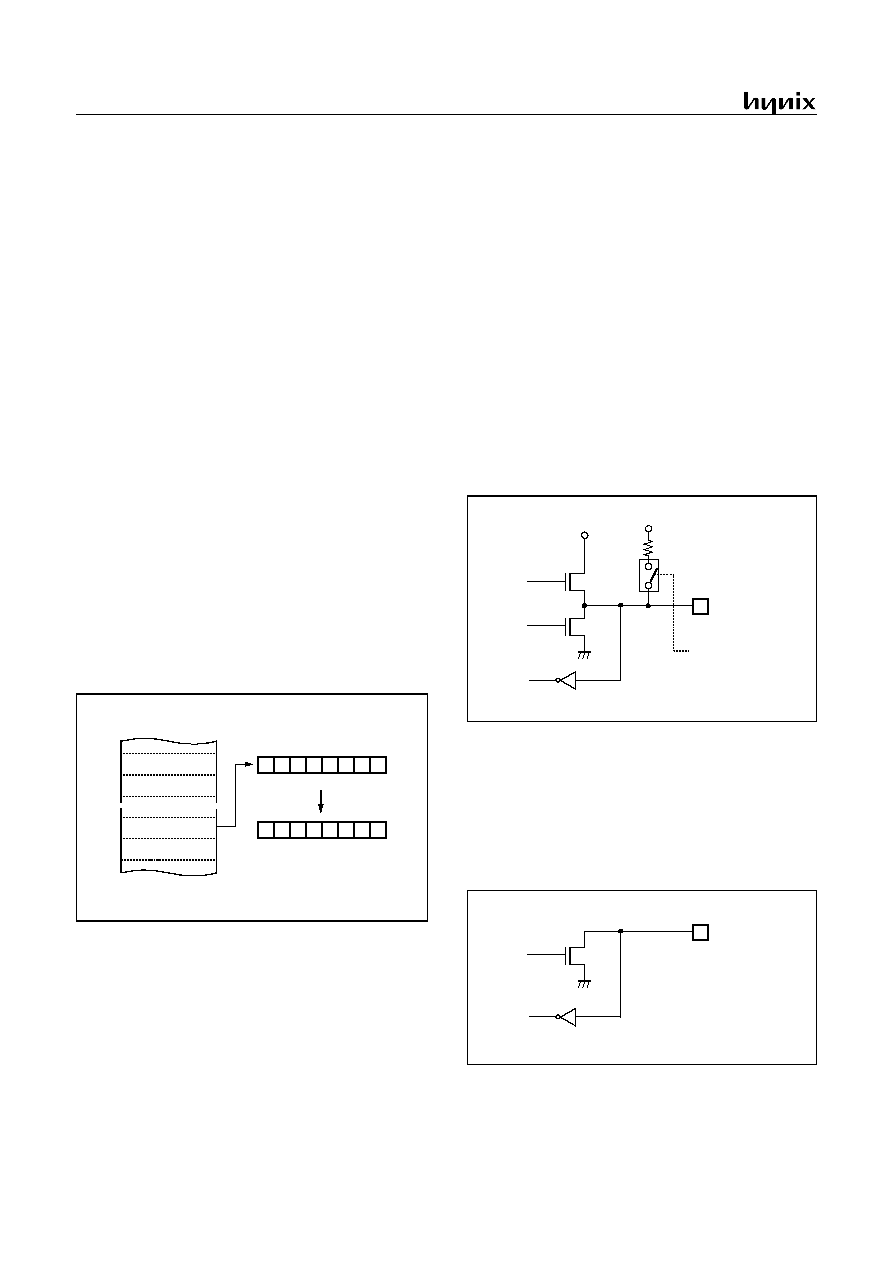
GMS81C7008/7016
32
APR., 2001 Ver 2.01
9. I/O PORTS
The GMS81C7008/16 has seven ports (R0, R1, R2, R3, R4, R5
and R6), and LCD segment port SEG0~SEG23, and LCD com-
mon p ort C OM 0~C OM3, wh ich ar e mul ti plex ed wit h
SEG24~SEG26.
These ports pins may be multiplexed with an alternate function
for the peripheral features on the device. In general, in a initial re-
set state, R0,R1,R2, R3 ports are used as a general purpose input
port and R4, R5, R6 and R7 ports are used as LCD segment drive
output port.
9.1 Registers for Port
Port Data Registers
The Port Data Registers in I/O buffer in each seven ports
(R0,R1,R2,R3,R4,R5,R6) are represented as a Type D flip-flop,
which will clock in a value from the internal bus in response to a
"write to data register" signal from the CPU. The Q output of the
flip-flop is placed on the internal bus in response to a "read data
register" signal from the CPU. The level of the port pin itself is
placed on the internal bus in response to "read data register" sig-
nal from the CPU. Some instructions that read a port activating
the "read register" signal, and others activating the "read pin" sig-
nal
Port Direction Registers
All pins have data direction registers which can define these ports
as output or input. A "1" in the port direction register configure
the corresponding port pin as output. Conversely, write "0" to the
corresponding bit to specify it as input pin. For example, to use
the even numbered bit of R0 as output ports and the odd num-
bered bits as input ports, write "55
H
" to address 0C8
H
(R0 port
direction register) during initial setting as shown in Figure 9-1.
Figure 9-1 Example of port I/O assignment
All the port direction registers in the MCU have 0 written to them
by reset function. On the other hand, its initial status is input.
Pull-up Control Registers
The R0, R1, R2 and R3 ports have internal pull-up resistors.
Figure 9-2 shows a functional diagram of a typical pull-up port.
It is connected or disconnected by Pull-up Control register
(PURn). The value of that resistor is typically 180k
.
When a port is used as input, input logic is firmly either low or
high, therefore external pull-down or pull-up resisters are re-
quired practically. The GMS81C7008/16 has internal pull-up, it
can be logic high by pull-up that can be able to configure either
connect or disconnect individually by pull-up control registers
R0PU, R1PU, R2PU and R3PU.
When ports are configured as inputs and pull-up resistor is select-
ed by software, they are pulled to high.
Figure 9-2 Pull-up Port Structure
Open drain port Registers
The R0, R1, R2 and R3 ports have open drain port resistors
R0CR~R3CR.
Figure 9-3 shows a open drain port configuration by control reg-
ister. It is selected as either push-pull port or open-drain port by
R0CR, R1CR, R2CR and R3CR.
Figure 9-3 Open-drain Port Structure
I : INPUT PORT
WRITE "55
H
" TO PORT R0 DIRECTION REGISTER
0
1
0
1
0
1
0
1
I
O
I
O
I
O
I
O
R0 DATA
R0 DIRECTION
R1 DATA
R1 DIRECTION
0C0H
0C1H
0C8H
0C9H
7
6
5
4
3
2
1
0
BIT
7
6
5
4
3
2
1
0
PORT
O : OUTPUT PORT
~
~
~
~
PULL-UP RESISTOR
PORT PIN
1: Connect
0: Disconnect
Pull-up control bit
VDD
GND
VDD
Typ. 160k
PORT PIN
1: Open drain
0: Push-pull
Open drain port selection bit
GND
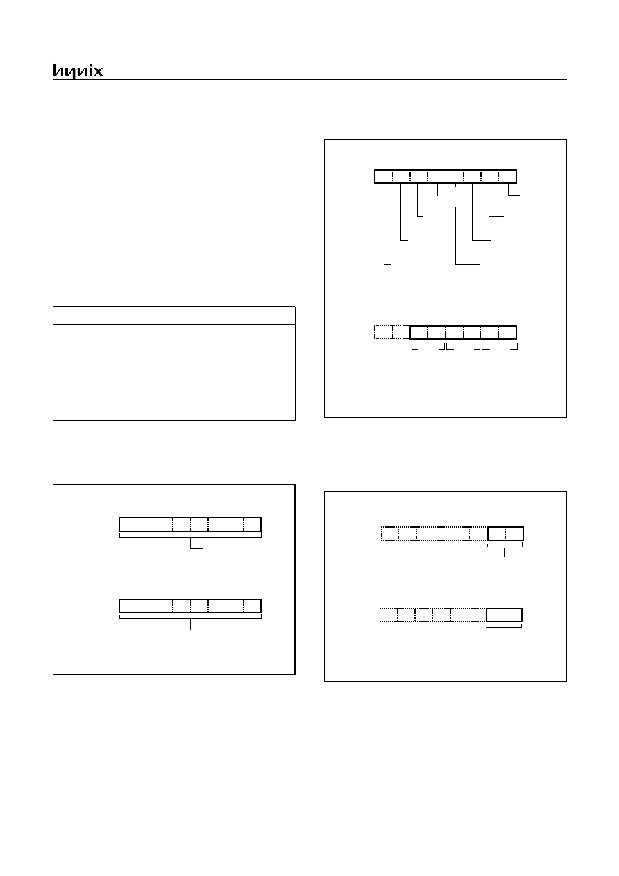
GMS81C7008/7016
APR., 2001 Ver 2.01
33
9.2 I/O Ports Configuration
R0 and R0DD register: R0 is an 8-bit CMOS bidirectional I/O
port (address 0C0
H
). Each I/O pin can independently used as an
input or an output through the R0DD register (address 0C8
H
).
Each port also can be set individually as pull-up port through the
R0PU (address 0D0
H
), and as open drain register through the
R0CR (address 0D4
H
).
In addition, port R0 is multiplexed with various special features.
The control register through the PMR (address 0D9
H
) and the
SIOM (address 0FE
H
) control the selection of alternate function.
After reset, this value is "0", port may be used as normal I/O port.
To use alternate function such as external interrupt, event counter
input, serial interface data input, serial interface data output or se-
rial interface clock, write "1" in the corresponding bit of PMR
(address 0D9
H
) and SIOM (address 0FE
H
).
Regardless of the direction register R0DD, the control registers of
PMR and SIOM are selected to use as alternate functions, port pin
can be used as a corresponding alternate features
.
R1 and R1DD register: R1 is an 2-bit CMOS bidirectional I/O
port (address 0C1
H
). Each I/O pin can independently used as an
input or an output through the R1DD register (address 0C9
H
).
Each port also can be set individually as pull-up port through the
R1PU (address 0D1
H
), and as open drain register through the
R1CR (address 0D5
H
).
Port pin
Alternate function
R00
R01
R02
R03
R04
R05
R06
R07
INT0 (External interrupt 0)
INT1 (External interrupt 1)
INT2 (External interrupt 2)
EC0 (Event counter input 0)
EC2 (Event counter input 2)
SCK (Serial clock)
SO (Serial data output)
SI (Serial data input)
R0 Data Register
R0
ADDRESS: 0C0
H
RESET VALUE: 00
H
R07 R06 R05 R04 R03 R02 R01 R00
Port Direction
R0 Direction Register
R0DD
ADDRESS: 0C8
H
RESET VALUE: 00
H
0: Input
1: Output
Input / Output data
Port Mode Register
PMR
ADDRESS: 0D9
H
RESET VALUE: 00
H
0: R00
1: INT0
0
0: R01
1: INT1
0: R02
1: INT2
0: R03
1: EC0
0: R04
1: EC2
0: R30
1: BUZ
0: R31
1: PWM0/T1O
0: R32
1: PWM1/T3O
1
2
3
4
5
6
7
Edge Detection Register
IEDS
ADDRESS: 0D8
H
RESET VALUE: 00
H
0
1
2
3
4
5
-
-
INT0
INT1
INT2
External Interrupt Edge Select
00: Reserved
01: Falling (1-to-0 transition)
10: Rising (0-to-1 transition)
11: Both (Rising & Falling)
R1 Data Register
R1
ADDRESS: 0C1
H
RESET VALUE: 00
H
R01 R00
Port Direction
R1 Direction Register
R1DD
ADDRESS: 0C9
H
RESET VALUE: 00
H
0: Input
1: Output
Input / Output data
-
-
-
-
-
-
-
-
-
-
-
-
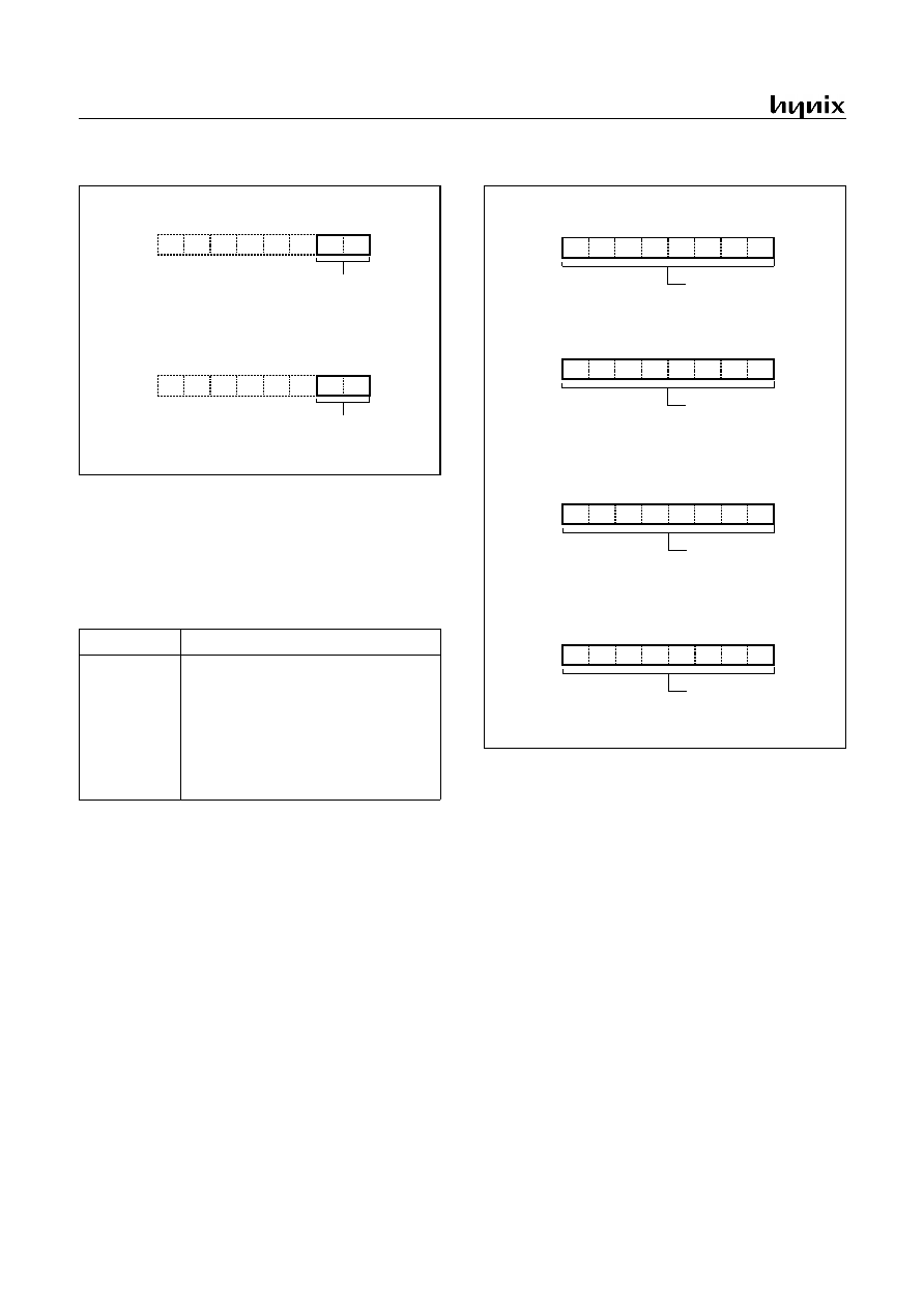
GMS81C7008/7016
34
APR., 2001 Ver 2.01
R2 and R2DD register: R2 is an 8-bit CMOS bidirectional I/O
port (address 0C2
H
). Each I/O pin can independently used as an
input or an output through the R2DD register (address 0CA
H
).
Each port also can be set individually as pull-up port through the
R2PU (address 0D2
H
), and as open drain register through the
R2CR (address 0D6
H
).
In addition, port R2 is multiplexed with analog input port.
Port pin
Alternate function
R20
R21
R22
R23
R24
R25
R26
R27
AN0 (Analog Input 0)
AN1 (Analog Input 1)
AN2 (Analog Input 2)
AN3 (Analog Input 3)
AN4 (Analog Input 4)
AN5 (Analog Input 5)
AN6 (Analog Input 6)
AN7 (Analog Input 7)
Port Pull-up
R1 Pull-up Register
R1PU
ADDRESS: 0D1
H
RESET VALUE: 00
H
0: Pull-up resistor Off
1: Pull-up resistor On
Port Open drain
R1 Open drain control Register
R1CR
ADDRESS: 0D5
H
RESET VALUE: 00
H
0: Push Pull
1: Open drain
-
-
-
-
-
-
-
-
-
-
-
-
R2 Data Register
R2
ADDRESS: 0C2
H
RESET VALUE: 00
H
R07 R06 R05 R04 R03 R02 R01 R00
Port Direction
R2 Direction Register
R2DD
ADDRESS: 0CA
H
RESET VALUE: 00
H
0: Input
1: Output
Input / Output data
Port Pull-up
R2 Pull-up Register
R2PU
ADDRESS: 0D2
H
RESET VALUE: 00
H
0: Pull-up resistor Off
1: Pull-up resistor On
Port Open drain
R2 Open drain control Register
R2CR
ADDRESS: 0D6
H
RESET VALUE: 00
H
0: Push Pull
1: Open drain
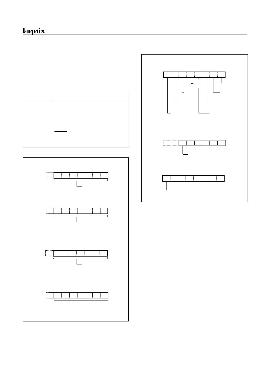
GMS81C7008/7016
APR., 2001 Ver 2.01
35
R3 and R3DD register: R3 is an 8-bit CMOS bidirectional I/O
port (address 0C3
H
). Each I/O pin can independently used as an
input or an output through the R3DD register (address 0CB
H
).
Each port also can be set individually as pull-up port through the
R3PU (address 0D3
H
), and as open drain register through the
R3CR (address 0D7
H
).
In addition, port R3 is multiplexed with various special features.
Port pin
Alternate function
R30
R31
R32
R33
R34
R35
R36
BUZ (Buzzer driving output)
PWM0 / T1O (PWM 0 output
/ Timer 1 output)
PWM1 /T3O (PWM 1 output
/ Timer 3 output)
-
WDTO (Watchdog timer output)
SX
OUT
(Sub clock output)
SX
IN
(Sub clock input)
R3 Data Register
R3
ADDRESS: 0C3
H
RESET VALUE: 00
H
Port Direction
R3 Direction Register
R3DD
ADDRESS: 0CB
H
RESET VALUE: 00
H
0: Input
1: Output
Input / Output data
Port Pull-up
R3 Pull-up Register
R3PU
ADDRESS: 0D3
H
RESET VALUE: 00
H
0: Pull-up resistor Off
1: Pull-up resistor On
Port Open drain
R3 Open drain control Register
R3CR
ADDRESS: 0D7
H
RESET VALUE: 00
H
0: Push Pull
1: Open drain
-
-
-
-
R06 R05 R04 R03 R02 R01 R00
Port Selection Register
PMR
ADDRESS: 0D9
H
RESET VALUE: 00
H
0: R00
1: INT0
0
0: R01
1: INT1
0: R02
1: INT2
0: R03
1: EC0
0: R04
1: EC2
0: R30
1: BUZ
0: R31
1: PWM0/T1O
0: R32
1: PWM1/T3O
1
2
3
4
5
6
7
Watch Dog Timer Register
WDTR
ADDRESS: 0DF
H
RESET VALUE: --01_0010
B
WDCLR
WDOM
WDCK0
WDCK1
WDEN
WDOE
-
-
LCD Control Register
LCR
ADDRESS: 0F1
H
RESET VALUE: 00
H
LCK0
LCK1
DTY0
DTY1
BRC
LCDEN
BTC
S U BM
0: R34
1: WDTO
0: SX
OUT
, SX
IN
(Sub Clock Oscillation)
1: R35, R36(Sub Clock Disable)
GMS81C7008/7016
36
APR., 2001 Ver 2.01
R4 and R4DD register: R4 is an 8-bit CMOS bidirectional I/O
port (address 0C4
H
). Each I/O pin can independently used as an
input or an output through the R4DD register (address 0CC
H
).
A f ter R e s e t , R 4 p o rt i s u s e d a s L C D s e g m e n t o ut p u t
SEG0~SEG7. To use general I/O ports user should be written ap-
propriate value into the LPMR (0F3
H
).
R5 and R5DD register: R5 is an 8-bit CMOS bidirectional I/O
port (address 0C5
H
). Each I/O pin can independently used as an
input or an output through the R4DD register (address 0CD
H
).
A f ter R e s e t , R 5 p o rt i s u s e d a s L C D s e g m e n t o ut p u t
SEG8~SEG15. To use general I/O ports user should be written
appropriate value into the LPMR (0F3
H
).
R6 and R6DD register: R6 is an 8-bit CMOS bidirectional I/O
port (address 0C6
H
). Each I/O pin can independently used as an
input or an output through the R6DD register (address 0CE
H
).
Af t er Re set, R 6 p or t is u s ed a s LC D s eg m en t outpu t
SEG16~SEG23. To use general I/O ports user should be written
appropriate value into the LPMR (0F3
H
).
LCD pin function
Port pin
SEG0 (LCD segment 0 signal output)
SEG1 (LCD segment 1 signal output)
SEG2 (LCD segment 2 signal output)
SEG3 (LCD segment 3 signal output)
SEG4 (LCD segment 4 signal output)
SEG5 (LCD segment 5 signal output)
SEG6 (LCD segment 6 signal output)
SEG7 (LCD segment 7 signal output)
R40
R41
R42
R43
R44
R45
R46
R47
LCD pin function
Port pin
SEG8 (LCD segment 8 signal output)
SEG9 (LCD segment 9 signal output)
SEG10 (LCD segment 10 signal output)
SEG11 (LCD segment 11 signal output)
SEG12 (LCD segment 12 signal output)
SEG13 (LCD segment 13 signal output)
SEG14 (LCD segment 14 signal output)
SEG15 (LCD segment 15 signal output)
R50
R51
R52
R53
R54
R55
R56
R57
R4 Data Register
R4
ADDRESS: 0C4
H
RESET VALUE: 00
H
R47 R46 R45 R44 R43 R42 R41 R40
Port Direction
R4 Direction Register
R4DD
ADDRESS: 0CC
H
RESET VALUE: 00
H
0: Input
1: Output
Input / Output data
LCD pin function
Port pin
SEG16 (LCD segment 16 signal output)
SEG17 (LCD segment 17 signal output)
SEG18 (LCD segment 18 signal output)
SEG19 (LCD segment 19 signal output)
SEG20 (LCD segment 20 signal output)
SEG21 (LCD segment 21 signal output)
SEG22 (LCD segment 22 signal output)
SEG23 (LCD segment 23 signal output)
R60
R61
R62
R63
R64
R66
R66
R67
R5 Data Register
R5
ADDRESS: 0C5
H
RESET VALUE: 00
H
R57 R56 R55 R54 R53 R52 R51 R50
Port Direction
R5 Direction Register
R5DD
ADDRESS: 0CD
H
RESET VALUE: 00
H
0: Input
1: Output
Input / Output data
R6 Data Register
R6
ADDRESS: 0C6
H
RESET VALUE: 00
H
R67 R66 R65 R64 R63 R62 R61 R60
Port Direction
R6 Direction Register
R6DD
ADDRESS: 0CE
H
RESET VALUE: 00
H
0: Input
1: Output
Input / Output data
GMS81C7008/7016
APR., 2001 Ver 2.01
37
10. CLOCK GENERATOR
As shown in Figure 10-1, the clock generator produces the basic
clock pulses which provide the system clock to be supplied to the
CPU and the peripheral hardware. It contains two oscillators: a
main-frequency clock oscillator and a sub-frequency clock oscil-
lator. Power consumption can be reduced by switching them to
the low power operation frequency clock can be easily obtained
by attaching a resonator between the X
IN
and X
OUT
pin and the
SX
IN
and SX
OUT
pin, respectively. The system clock can also be
obtained from the external oscillator.
The clock generator produces the system clocks forming clock
pulse, which are supplied to the CPU and the peripheral hard-
ware. The internal system clock can be selected by bit2, and bit3
of the System Clock Mode Register(SCMR).
The register is shown in Figure 10-2.
To the peripheral block, the clock among the not-divided original
clocks, divided by 2
, 4,...,
up to 1024 can be provided. Peripheral
clock is enabled or disabled by STOP instruction.
Figure 10-1 Block Diagram of Clock Generator
CPU clock
Instruction cycle time
X
IN
= 4MHz
SX
IN
= 32.768kHz
÷
2
0.5 us
61 us
÷
8
2.0 us
244 us
÷
16
4.0 us
488 us
÷
64
16.0 us
1953 us
Internal system clock (CPU clock)
SX
IN
PIN
PRESCALER
0
1
X
IN
PIN
÷
1
Peripheral clock
MUX
÷
2
÷
4
÷
8
÷
16
÷
128
÷
256
÷
512
÷
1024
÷
32
÷
64
÷
2
÷
8
÷
16
÷
64
select clock
SCS[1:0]
OSC Stop
SYCC<1>
SYCC<0>
STOP Mode
SLEEP Mode
PS0
PS1
PS2
PS3
PS4
PS5
PS6
PS7
PS8
PS9
PS10
CL
O
C
K PUL
S
E
f
EX
(MHz)
PS0
PS3
PS2
PS4
PS1
PS10
PS9
PS5
PS6
PS7
4
Frequency
period
4M
1M
500K
250K
2M
125K
62.5K
250n
500n
1u
2u
4u
8u
16u
32u
64u
256u
128u
3.906K
7.183K
15.63K
31.25K
PS8
f
EX
LCR<7>
OSC Stop
G
E
NE
RAT
O
R
GMS81C7008/7016
38
APR., 2001 Ver 2.01
The system clock is decided by bit1 (SYCC1) of the system clock
mode register(SCMR). In selection Sub clock, to oscillate or stop
the Main clock is decided by bit0 (SYCC0) of SCMR. On the ini-
tial reset, internal system clock is PS1 which is the fastest and
other clock can be provided by bit2 and bit3 of SCMR.
Figure 10-2 SCMR: System Clock Control Registers
System (CPU) clock control
00: main clock on
01: main clock on
10: sub clock on (main clock on)
11: sub clock on (main clock off)
System clock source select
00: X
IN
÷
2
01: X
IN
÷
8
INITIAL VALUE: 00
H
ADDRESS: 0F5
H
SCMR
10: X
IN
÷
16
11: X
IN
÷
64
or SX
IN
÷
2
or SX
IN
÷
8
or SX
IN
÷
16
or SX
IN
÷
64
BTCL
7
6
5
4
3
2
1
0
-
-
SYCC1 SYCC0
R/W
R/W
R/W
R/W
SCS1 SCS0
-
-
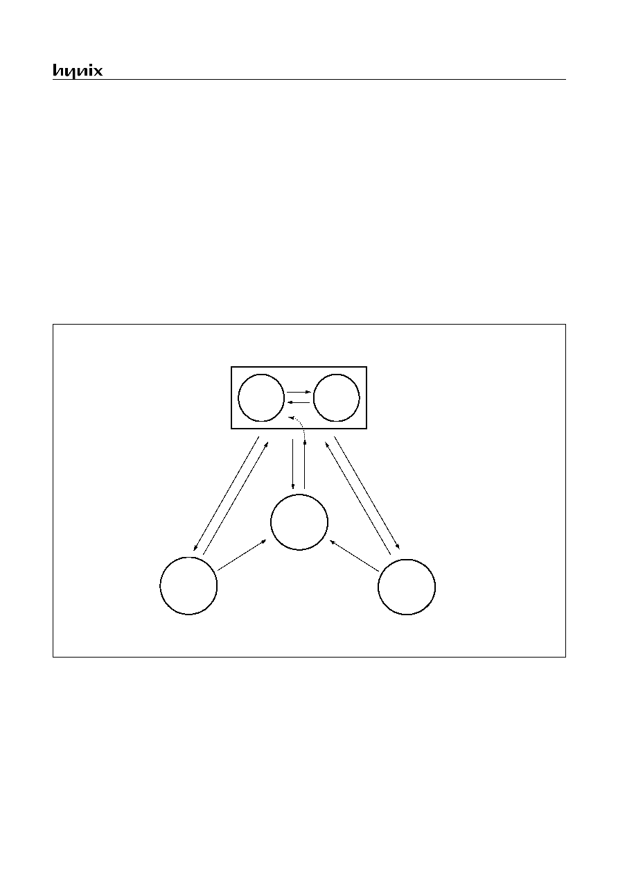
GMS81C7008/7016
APR., 2001 Ver 2.01
39
11. OPERATION MODE
The system clock controller starts or stops the main-frequency
clock oscillator and switches between the sub frequency clock.
The operating mode is generally divided into the main-clock
mode and the sub-clock mode, which are controlled by System
clock mode register (SCMR). Figure 11-1shows the operating
mode transition diagram.
System clock control is performed by the system clock mode reg-
ister, SCMR. During reset, this register is initialized to "0" so that
the main-clock operating mode is selected.
Main-clock operating mode
This mode is fast-frequency operating mode.
The CPU and the peripheral hardwares are operated on the high-
frequency clock. At reset release, this mode is invoked.
Sub-clock operating mode
This mode is low-frequency operating mode
In this mode, the high-frequency clock oscillation is stops and
low-frequency clock oscillation is active to operate the CPU and
the peripheral hardware on the low-frequency clock, thereby re-
ducing power consumption
SLEEP mode
In this mode, the CPU clock stops while peripherals and the os-
cillation source continue to operate normally.
STOP mode
In this mode, the system operations are all stopped, holding the
internal states valid immediately before the stop at the low power
consumption level.
Figure 11-1 Operating Mode
Main-clock
Mode
STOP
Mode
RESET
Operation
Re
se
t
Re
set
Main: According to SCMR
Sub: Oscillating
Main: Stopped
Sub: Oscillating
Main: Oscillating
Sub: Oscillating
SLEEP
Mode
Re
le
a
s
e
R
e
set
S
T
O
P
I
n
st
ru
ct
io
n
R
e
fe
r
to
n
o
te
1
In
str
u
cti
o
n
R
e
fe
r t
o
n
o
te
2
Main
Sub - Oscillating
- Oscillating
Main
Sub - Oscillating
- According to SCMR
Sub-clock
Mode
Instruction
Instruction
NOTE1:
RESET
Key Scan Int.
Watch Timer Int.
Timer interrupt (EC0, EC2)
External Int.
NOTE2:
RESET
All Int.
CPU stops,
Peripherals are operate.
CPU and Peripherals are stops,
SIO Int.
Watchdog Timer Int.

GMS81C7008/7016
40
APR., 2001 Ver 2.01
11.1 Operation Mode Switching
In the Main-clock operation mode, only the high-frequency clock
oscillator is used.
In the Sub-clock operation mode, the high-frequency clock oscil-
lation stops, enabling the low power voltage operation or the low
power consumption operation. Instruction execution does not
stop when the operation speed switching is performed. However,
some peripheral hardware capabilities may be affected. For de-
tails, refer to the description of the relevant operation.
The following describes the switching between the Main-clock
and the Sub-clock operations. During reset, the system clock
mode register is initialized at the Main-clock mode. It must be set
to the Sub-clock operation for the low-power consumption mode.
Switching from main clock operation to sub-
clock operation
First, write "10
B
" into lower 2 bits of SCMR to switch the main
system clock to the sub-frequency clock.
Next, write "11
B
" to turn off main frequency oscillation.
Example:
:
:
MOV
SCMR,#0000_XX10B
;
Switch to sub mode
MOV
SCMR,#0000_XX11B
;
Turn off main clock
:
:
Returning from sub clock operation to main
clock operation
First, write "10
B
" into lower 2 bits of the SCMR to turn on the
main-frequency oscillation, when the stabilization (warm-up) has
been taken by the software delay routine. Sub clock operation
mode can also be released by setting the RESET pin to low,
which immediately performs the reset operation. After reset, the
GMS81C7008/16 is placed in main frequency operation mode.
Example:
:
:
:
MOV
SCMR,#0000_XX10B
;
Turn on main-clock
CALL DELAY
;
Wait until stable
MOV
SCMR,#0000_XX00B
;
Move to main mode
:
:
:
;20ms software delay at fXIN=4MHz
DELAY:
LDY
#0
DLP0:
LDA
#0
DLP1:
NOP
INC
A
BCC
DLP1
INC
Y
CMPY
#20
BCC
DLP0
RET
Shifting from the Normal operation to the SLEEP
mode
By setting bit 0 of SMR, the CPU clock stops and the SLEEP
mode is invoked. The CPU stops while other peripherals are op-
erate normally.
The way of release from this mode is RESET and all available in-
terrupts.
For more detail, See "20.1 SLEEP Mode" on page 81
Shifting from the Normal operation to the STOP
mode
By executing STOP instruction, the main-frequency clock oscil-
lation stops and the STOP mode is invoked. But sub-frequency
clock oscillation is operated continuously.
After the STOP operation is released by reset, the operation mode
is changed to Main-clock mode.
The methods of release are RESET, Key scan interrupt, Watch
Timer interrupt, Timer/Event counter1 (EC0, EC2 pin), and Ex-
ternal Interrupt.
For more details, see "20.2 STOP Mode" on page 82.
Note: In the STOP and Sub clock operating modes, the
power consumed by the oscillator and the internal hard-
ware is reduced. However, the power for the pin interface
(depending on external circuitry and program) is not directly
associated with the low-power consumption operation. This
must be considered in system design as well as interface
circuit design.
GMS81C7008/7016
APR., 2001 Ver 2.01
41
Figure 11-2 System Clock Switching Timing
Operation clock
~~
~~
Sub-clock operation
Main-clock operation
Sub freq. clock
Main freq. clock
(X
IN
pin)
(SX
IN
pin)
Changed to the Sub-clock
SCMR
XXXX XX10
B
~~
~~
~~
Operation clock
~~
Main-clock operation
Stabilizing Time
>
20ms
Sub freq. clock
Main freq. clock
(X
IN
pin)
(SX
IN
pin)
Changed to the Transition
Changed to the Main-clock
SCMR
XXXX XX10
B
SCMR
XXXX XX00
B
~~
~~
Sub-clock operation
~~
(a) Main clock mode
Sub clock mode
(b) Sub clock
Main clock
or 01
B
Turn off main clock
SCMR
XXXX XX11
B
GMS81C7008/7016
42
APR., 2001 Ver 2.01
12. BASIC INTERVAL TIMER
The GMS81C7008/16 has one 8-bit Basic Interval Timer that is
free-run and can not stop. Block diagram is shown in Figure 12-1.
In addition, the Basic Interval Timer generates the time base for
watchdog timer counting. It also provides a Basic interval timer
interrupt (BITIF). As the count overflow from FF
H
to 00
H
, this
overflow causes the interrupt to be generated. The Basic Interval
Timer is controlled by the clock control register (CKCTLR)
shown in Figure 12-2.
Source clock can be selected by lower 3 bits of CKCTLR.
The registers BITR and CKCTLR are located at same address,
and address 0F9
H
is read as a BITR, and written to CKCTLR.
Figure 12-1 Block Diagram of Basic Interval Timer
Table 12-1 Basic Interval Timer Interrupt Time
MUX
Basic Interval Timer Interrupt
Select Input clock 3
Basic Interval Timer
source
clock
8-bit up-counter
BTS[2:0]
BTCL
÷
8
÷
1024
÷
512
÷
256
÷
128
÷
64
÷
32
÷
16
To Watchdog timer (WDTCK)
CKCTLR
clear
overflow
Internal bus line
clock control register
[0F4
H
]
[0F9
H
]
BITIF
Read
Pr
esca
ler
BITR
f
XIN
f
SXIN
0X
1X
SCMR[1:0]
BTS[2:0]
CPU Source clock
Interrupt (overflow) Period (ms)
@ f
XIN
= 4MHz
@ f
SXIN
= 32.768kHz
000
001
010
011
100
101
110
111
÷
8
÷
16
÷
32
÷
64
÷
128
÷
256
÷
512
÷
1024
0.512
1.024
2.048
4.096
8.192
16.384
32.768
65.536
62.5ms
125ms
250ms
500ms
1000ms
2000ms
4000ms
8000ms
GMS81C7008/7016
APR., 2001 Ver 2.01
43
Figure 12-2 BITR: Basic Interval Timer Mode Register
Example 1:
Interrupt request flag is generated every 8.192ms at 4MHz.
:
LDM
CKCTLR,#0CH
SET1
BITE
EI
:
BTCL
7
6
5
4
3
2
1
0
-
-
BTS1
Basic Interval Timer source clock select
000: f
XIN
÷
8
001: f
XIN
÷
16
010: f
XIN
÷
32
011: f
XIN
÷
64
100: f
XIN
÷
128
101: f
XIN
÷
256
110: f
XIN
÷
512
111: f
XIN
÷
1024
Clear bit
0: Normal operation, free-run
1: Clear 8-bit counter (BITR) to "0" and count up again.
INITIAL VALUE: ---0 0111
B
ADDRESS: 0F4
H
CKCTLR
INITIAL VALUE: Undefined
ADDRESS: 0F4
H
BITR
Both register are in same address,
when write, to be a CKCTLR,
when read, to be a BITR.
Caution:
8-BIT FREE-RUN BINARY COUNTER
BTS0
BTS2
BTCL
BTCL
7
6
5
4
3
2
1
0
or f
SXIN
÷
8
or f
SXIN
÷
16
or f
SXIN
÷
32
or f
SXIN
÷
64
or f
SXIN
÷
128
or f
SXIN
÷
256
or f
SXIN
÷
512
or f
SXIN
÷
1024
R
W
W
W
W
W
R
R
R
R
R
R
R
BCK
-
This bit becomes to "0" automatically after one machine cycle.
For the test purpose.
This bit must be cleared to "0" for normal operation,
otherwise BIT clock source is form sub-clock.

GMS81C7008/7016
44
APR., 2001 Ver 2.01
13. TIMER/EVENT COUNTER
The GMS81C7008/16 has four Timer/Event counters. Each mod-
ule can generate an interrupt to indicate that an event has occurred
(i.e. timer match).
Timer 0 and Timer 1 are can be used either two 8-bit Timer/
Counter or one 16-bit Timer/Counter with combine them. Also
Timer 2 and Timer 3 can be joined as a 16-bit Timer/Counter.
In the "timer" function, the register is increased every internal
clock input. Thus, one can think of it as counting internal clock
input. The count rate is 1/2 to 1/2048 of the oscillator frequency.
In the "counter" function, the register is incremented in response
to a 0-to-1 (rising edge) transition at its corresponding external
input pin, EC0 or EC2 pin.
In addition the "capture" function, the register is incremented in
response external or internal clock sources same with timer or
counter function. When external clock edge input, the count reg-
ister is captured into Capture data register correspondingly.
It has five operating modes: "8-bit timer/counter", "16-bit timer/
counter", "8-bit capture", "16-bit capture", "PWM mode" which
are selected by bit in Timer mode register TMn.
In operation of Timer 2, Timer 3, their operations are same with
Timer 0, Timer 1, respectively.
When programming the software, you may refer to following ex-
ample.
Example 1:
Timer 0 = 8-bit timer mode, 8ms interval at 4MHz
Timer 1 = 8-bit timer mode, 4ms interval at 4MHz
Timer 2 = 16-bit event counter mode
LDM
SCMR,#0
;Main clock mode
LDM
TDR0,#249
LDM
TM0,#0001_0011B
LDM
TDR1,#124
LDM
TM1,#0000_1111B
LDM
TDR2,#1FH
LDM
TDR3,#4CH
LDM
TM2,#0001_1111B
LDM
TM3,#0100_1100B
SET1
T0E
SET1
T2E
EI
:
:
Example 2:
Timer0 = 16-bit timer mode, 0.5s at 4MHz
Timer2 = 2ms 8-bit timer mode at 4MHz
Timer3 = 250us 8-bit timer mode at 4MHz
LDM
SCMR,#0
;Main clock mode
LDM
TDR0,#23H
LDM
TDR1,#0F4H
LDM
TM0,#0FH
;FXIN/32, 8us
LDM
TM1,#4CH
LDM
TDR2,#249
LDM
TDR3,#124
LDM
TM2,#0FH
;FXUN/32, 8us
LDM
TM3,#0DH
;FXIN/8, 2us
SET1
T0E
SET1
T2E
SET1
T3E
EI
:
:
Example 3:
Timer0 = 8-bit timer mode, 2ms interval at 4MHz
Timer1 = 8-bit capture mode, 2us sampling count.
LDM
TDR0,#249
;250x8=2000us
LDM
TM0,#0FH
;FXIN/32, 8us
LDM
IEDS,#XXXX_01XXB ;FALLING
LDM
PMR,#XXXX_XX1XB ;AS INT1
LDM
TDR1,#0FFH
LDM
TM1,#0001_1011B ;2us
SET1
T0E
;ENABLE TIMER 0
SET1
T1E
;ENABLE TIMER 1
SET1
INT1E
;ENABLE EXT. INT1
EI
:
:
X: don't care.
Example 4:
Timer0 = 8-bit timer mode, 2ms interval at 4MHz
Timer2 = 16-bit capture mode, 8us sampling count.
LDM
TDR0,#249
LDM
TM0,#0FH
LDM
IEDS,#XX11_XXXXB
LDM
PMR4,#XXXX_X1XXB
LDM
TDR2,#0FFH ;MAX
LDM
TDR3,#0FFH ;MAX
LDM
TM2,#XX10_1111B ;/32
LDM
TM3,#X10X_11XXB
SET1
T0E
;ENABLE TIMER 0
SET1
T2E
;ENABLE TIMER 2
SET1
INT2E
;ENABLE EXT. INT2
EI
:
:
X: don't care.
GMS81C7008/7016
APR., 2001 Ver 2.01
45
Figure 13-1 TM0, TM1, TDRn Registers
B TC L
7
6
5
4
3
2
1
0
C AP 0
T0C K1
INITIAL VALUE: 00
H
ADDRESS: 0E0
H
TM0
T 0C K0 T0C N
T0S T
7
6
5
4
3
2
1
0
INITIAL VALUE: 0FF
H
ADDRESS: 0E1
H
, 0E3
H
, 0E7
H
, 0E9
H
TDR0~TDR3
Compare data registers
W
W
W
W
W
W
W
W
R/W
R/W
R/W
R/W
R/W
R/W
T0C K2
Timer 0 mode register
Basic Interval Timer source clock select
000: f
XIN
÷
2
001: f
XIN
÷
4
010: f
XIN
÷
8
011: f
XIN
÷
32
100: f
XIN
÷
128
101: f
XIN
÷
512
110: f
XIN
÷
2048
111: EC0 (External event input 0)
0: Disable count
1: Enable count
0: stop count
1: clearing the T0 counter and start count again
Timer/Counter 0 enable flag
Timer/Counter 0 start/stop control flag
0: Timer mode
1: Capture mode
Capture mode enable
-
-
B TC L
7
6
5
4
3
2
1
0
PW M E0
T1C K1
INITIAL VALUE: 00
H
ADDRESS: 0E2
H
TM1
T1C K0 T1C N
T 1S T
R/W
R/W
R/W
R/W
R/W
R/W
C A P1
Timer 1 mode register
Timer/Counter 1 source clock select
00: f
XIN
01: f
XIN
÷
2
10: f
XIN
÷
8
11: Timer 0 clock
0: Disable count
1: Enable count
0: stop count
1: clearing the T1 counter and start count again
Timer/Counter 1 enable flag
Timer/Counter 1 start/stop control flag
0: Timer mode
1: Capture mode
Capture mode enable
PO L0 16BIT 0
R/W
R/W
0: Disable
1: Enable
PWM enable bit
0: Active low
1: Active high
PWM duty control
0: 8-bit mode
1: 16-bit mode
Mode selection
or f
SXIN
or f
SXIN
÷
2
or f
SXIN
÷
8
(depend on SCMR)
or f
SXIN
÷
2
or f
SXIN
÷
4
or f
SXIN
÷
8
or f
SXIN
÷
32
or f
SXIN
÷
128
or f
SXIN
÷
512
or f
SXIN
÷
2048
GMS81C7008/7016
46
APR., 2001 Ver 2.01
Figure 13-2 TM2, TM3 Registers
B TC L
7
6
5
4
3
2
1
0
C AP 2
T2C K1
INITIAL VALUE: 00
H
ADDRESS: 0E6
H
TM2
T 2C K0 T 2C N
T2S T
R/W
R/W
R/W
R/W
R/W
R/W
T2C K2
Timer 2 mode register
Timer/Counter 2 source clock select
000: f
XIN
÷
2
001: f
XIN
÷
4
010: f
XIN
÷
8
011: f
XIN
÷
32
100: f
XIN
÷
128
101: f
XIN
÷
512
110: f
XIN
÷
2048
111: EC2 (External event input 2)
0: Disable count
1: Enable count
0: stop count
1: clearing the T0 counter and start count again
Timer/Counter 2 enable flag
Timer/Counter 2 start/stop control flag
0: Timer mode
1: Capture mode
Capture mode enable
-
-
B TC L
7
6
5
4
3
2
1
0
PW M E1
T3C K1
INITIAL VALUE: 00
H
ADDRESS: 0E8
H
TM3
T 3C K0 T3C N
T 3S T
R/W
R/W
R/W
R/W
R/W
R/W
C A P3
Timer 3 mode register
Timer/Counter 3 source clock selection
0: Disable count
1: Enable count
0: stop count
1: clearing the T3 counter and start count again
Timer/Counter 3 enable flag
Timer/Counter 3 start/stop control flag
0: Timer mode
1: Capture mode
Capture mode enable
PO L1 16B IT 1
R/W
R/W
0: Disable
1: Enable
PWM enable bit
0: Active low
1: Active high
PWM1 duty control
0: 8-bit mode
1: 16-bit mode
Mode selection
00: f
XIN
01: f
XIN
÷
2
10: f
XIN
÷
8
11: Timer 2 clock
or f
SXIN
or f
SXIN
÷
2
or f
SXIN
÷
8
(depend on SCMR)
or f
SXIN
÷
2
or f
SXIN
÷
4
or f
SXIN
÷
8
or f
SXIN
÷
32
or f
SXIN
÷
128
or f
SXIN
÷
512
or f
SXIN
÷
2048
7
6
5
4
3
2
1
0
INITIAL VALUE: 00
H
ADDRESS: 0E1
H
, 0E4
H
, 0E7
H
, 0EA
H
T0~T3
Count registers
R
R
R
R
R
R
R
R
CDR0~CDR3
GMS81C7008/7016
APR., 2001 Ver 2.01
47
13.1 8-bit Timer / Counter Mode
The GMS81C7008/16 has four 8-bit Timer/Counters, Timer 0,
Timer 1, Timer 2, Timer 3 which are shown in Figure 13-3, Fig-
ure 13-4.
The "timer" or "counter" function is selected by control registers
TMn. To use as an 8-bit timer/counter mode, CAP0, CAP1,
16BIT0 and PWME bits should be cleared to "0". These timers
have each 8-bit count register and data register. The count register
is increased by every internal or external clock input. The internal
clock has a prescaler divide ratio option of 2~2048 selected by
control bits of register TMn (n=0,1,2,3).
Figure 13-3 8-bit Timer/Counter 0, 1
EC0 PIN
÷
2
÷
4
÷
8
MUX
Pres
caler
T0IF
clear
0: Stop
1: Clear and start
000
001
010
TIMER 0
INTERRUPT
MUX
T1IF
clear
0: Stop
1: Clear and start
TIMER 1
INTERRUPT
÷
8
÷
2
÷
1
TDR0 (8-bit)
T1 (8-bit)
TDR1 (8-bit)
T0 (8-bit)
Comparator
Comparator
TIMER 0
TIMER 1
R31/T1O/PWM0
F/F
BTCL
7
6
5
4
3
2
1
0
-
CAP0
T0CK1
INITIAL VALUE: 00
H
ADDRESS: 0E0
H
TM0
T0CK0 T0CN T0ST
-
T0CK2
X
X
X means don't care
0
PIN
÷
32
÷
128
÷
512
÷
2048
011
100
101
110
111
00
01
10
11
BTCL
POL0
PW M E0
T1CK1
INITIAL VALUE: 00
H
ADDRESS: 0E2
H
TM1
T1CK0 T1CN T1ST
16BIT0
CAP1
X
0
0
0
Edge Detector
PMR.6
f
XIN
f
SXIN
0X
1X
SCMR[1:0]
X
X
X
X
X
X
X
X
X
T0CN
T0CK[2:0]
1
0
T0ST
T1ST
T1CN
1
0
T1CK[1:0]
[0D9
H
.6]
[0E1
H
]
[0E1
H
]
[0E4
H
]
[0E3
H
]
GMS81C7008/7016
48
APR., 2001 Ver 2.01
Note: The contents of Timer data register TDRx should be
initialized with 1
H
~FF
H
, not to 0
H
, because it is not to de-
fined before reset.
In the Timer 0, timer register T0 increments from 00
H
until it
matches with TDR0 and then reset to 00
H
. The match output of
Timer 0 generates Timer 0 interrupt (latched in T0IF bit)
As TDRx and Tx register are in same address, when reading it as
a Tx, written to TDRx.
In counter function, the counter is increased every 0-to-1 (rising
edge) transition of EC0 or EC2 pin. In order to use counter func-
tion, the bit 3 and bit 4 of the Port mode register PMR are set to
"1" by software. The Timer 0 can be used as a counter by pin EC0
input. Similarly, Timer 2 can be used by pin EC2 input.
Figure 13-4 8-bit Timer/Counter 2, 3
EC2 PIN
÷
2
÷
4
÷
8
MUX
P
r
esca
ler
T2IF
clear
0: Stop
1: Clear and start
000
001
010
TIMER 2
INTERRUPT
MUX
T3IF
clear
0: Stop
1: Clear and start
TIMER 3
INTERRUPT
÷
8
÷
2
÷
1
TDR2 (8-bit)
T3 (8-bit)
TDR3 (8-bit)
T2 (8-bit)
Comparator
Comparator
TIMER 2
TIMER 3
R32/T3O/PWM0
F/F
BTCL
7
6
5
4
3
2
1
0
-
CAP2
T2CK1
INITIAL VALUE: 00
H
ADDRESS: 0E6
H
TM2
T2CK0 T2CN T2ST
-
T2CK2
X
X
X means don't care
0
PIN
÷
32
÷
128
÷
512
÷
2048
011
100
101
110
111
00
01
10
11
BTCL
POL1
PWME1
T3CK1
INITIAL VALUE: 00
H
ADDRESS: 0E8
H
TM3
T3CK0 T3CN T3ST
16BIT1
CAP3
X
0
0
0
Edge Detector
PMR.7
f
XIN
f
SXIN
0X
1X
SCMR[1:0]
X
X
X
X
X
X
X
X
X
T2CN
T2CK[2:0]
1
0
T2ST
T3ST
T3CN
1
0
T3CK[1:0]
[0D9
H
.7]
[0E7
H
]
[0E7
H
]
[0EA
H
]
[0E9
H
]
GMS81C7008/7016
APR., 2001 Ver 2.01
49
8-bit Timer Mode
In the timer mode, the internal clock is used for counting up.
Thus, you can think of it as counting internal clock input. The
contents of TDRn (n=0,1,2,3) are compared with the contents of
up-counter, Tn (n=0,1,2,3). If match is found, a timer 1 interrupt
(T1IF) is generated and the up-counter is cleared to 0. Counting
up is resumed after the up-counter is cleared.
As the value of TDRn can be re-written by software, time interval
is set as you want
Figure 13-5 Timer Mode Timing Chart
Figure 13-6 Timer Count Example
0
n-2
2
0
n
3
n-1
n
Source clock
Up-counter
TDR1
T1IF interrupt
Start count
1
2
3
1
4
Match
Detect
Counter
Clear
~~
~~
~~
~~
~~
~~
Timer 1 (T1IF)
Interrupt
TDR1
TIME
Occur interrupt
Occur interrupt
Occur interrupt
Interrupt period
up-
count
~~
~~
0
1
2
3
4
5
6
7A
7D
7C
Count Pulse
= 8
µ
s x 125
7B
MATCH
Example: Make 1ms
interrupt using by Timer0 at 4MHz
LDM
TM0,#0FH
; divide by 32
LDM
TDR0,#124
; 8us x (124+1)= 1ms
SET1
T0E
; Enable Timer 0 Interrupt
EI
; Enable Master Interrupt
Period
When
TDR0 = 124
D
= 7C
H
f
XIN
= 4 MHz
INTERRUPT PERIOD =
4
×
106 Hz
1
×
32
×
(124+1) = 1 ms
TM0 = 0000_1111
B
(8-bit Timer mode, Prescaler divide ratio
÷
32)
8
µ
s
(TDR0 = T0)
7D
0
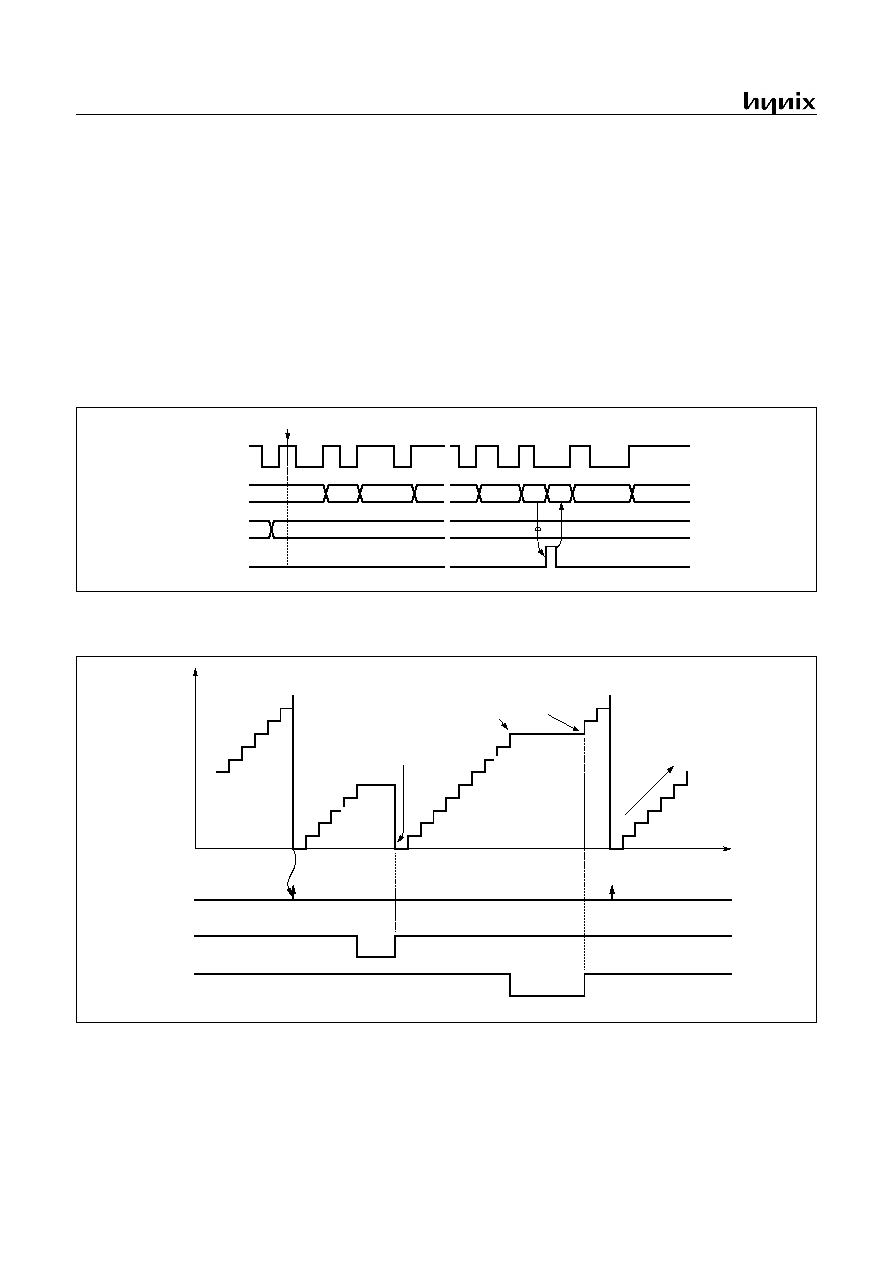
GMS81C7008/7016
50
APR., 2001 Ver 2.01
8-bit Event Counter Mode
In this mode, counting up is started by an external trigger. This
trigger means rising edge of the EC0 or EC2 pin input. Source
clock is used as an internal clock selected with timer mode regis-
ter TM0, TM1, TM2 or TM3. The contents of timer data register
TDRn (n = 0,1,2,3,........,FF) are compared with the contents of
the up-counter Tn. If a match is found, an timer interrupt request
flag TnIF is generated, and the counter is cleared to "0". The
counter is restart and count up continuously by every rising edge
of the ECn pin input.
The maximum frequency applied to the ECn pin is f
XIN
/2 [Hz].
In order to use event counter function, the bit 3, 4 of the Port
Mode Register PMR (address 0D9
H
) is required to be set to "1".
After reset, the value of timer data register TDRn is undefined, it
should be initialized to between 1
H
~FF
H
not to "0". The interval
period of Timer is calculated as below equation.
Figure 13-7 Event Counter Mode Timing Chart
Figure 13-8 Count Operation of Timer / Event counter
Period (sec)
1
f
XIN
----------
2
Divide Ratio
TDRn
×
×
×
=
0
1
2
1
0
n
2
~~
~~
~~
n-1
n
~~
~~
~~
ECn pin input
Up-counter
TDR1
T1IF interrupt
Start count
Timer 1 (T1IF)
Interrupt
TDR1
TIME
Occur interrupt
Occur interrupt
stop
clear & start
disable
enable
Start & Stop
T1ST
T1CN
Control count
up
-c
oun
t
~~
~~
T1ST = 0
T1ST = 1
T1CN = 0
T1CN = 1
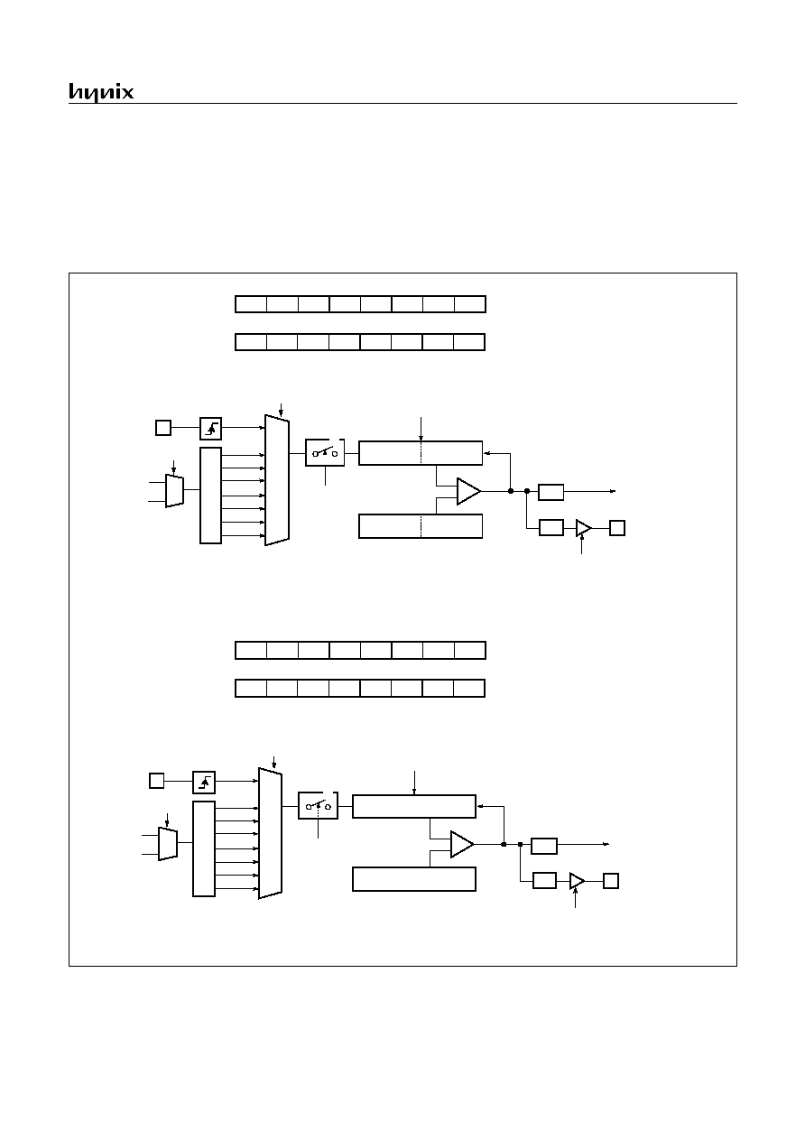
GMS81C7008/7016
APR., 2001 Ver 2.01
51
13.2 16-bit Timer / Counter Mode
The Timer register is being run with all 16 bits. A 16-bit timer/
counter register T0, T1 are incremented from 0000
H
until it
matches TDR0, TDR1 and then resets to 0000
H
. The match out-
put generates Timer 0 interrupt.
The clock source of the Timer 0 is selected either internal or ex-
ternal clock by bit T0SL1, T0SL0.
Even if the Timer 0 (including the Timer 1) is used as a 16-bit
timer, the Timer 2 and Timer 3 can still be used as either two 8-
bit timer or one 16-bit timer by setting the TM2. Reversely, even
if the Timer 2 (including the Timer 3) is used as a 16-bit timer,
the Timer 0 and Timer 1 can still be used as 8-bit timer indepen-
dently.
Figure 13-9 16-bit Timer/Counter
T0IF
clear
0: Stop
1: Clear and start
T0ST
T0CK[2:0]
TIMER 0 INTERRUPT
T0CN
Comparator
TIMER 0 + TIMER 1
TIMER 0 (16-bit)
Higher byte
Lower byte
COMPARE DATA
T0
(16-bit)
1
0
(Not Timer 1 interrupt)
7
6
5
4
3
2
1
0
INITIAL VALUE: 00
H
ADDRESS: 0E0
H
TM0
X
X
X
X
X
X
0
X
X means don't care
÷
2
÷
4
÷
8
MUX
Pr
esca
l
e
r
000
001
010
÷
32
÷
128
÷
512
÷
2048
011
100
101
110
111
Edge Detector
EC0 PIN
TM1
BTCL
X
1
0
0
1
1
X
X
POL0
PWME0
T1CK1
INITIAL VALUE: 00
H
ADDRESS: 0E2
H
T1CK0 T1CN T1ST
16BIT0
CAP1
BTCL
-
CAP0
T0CK1 T0CK0 T0CN T0ST
-
T0CK2
7
6
5
4
3
2
1
0
INITIAL VALUE: 00
H
ADDRESS: 0E6
H
TM2
X
X
X
X
X
X
0
X
TM3
BTCL
X
1
0
0
1
1
X
X
POL1
PWME1
T3CK1
INITIAL VALUE: 00
H
ADDRESS: 0E8
H
T3CK0 T3CN T3ST
16BIT1
CAP3
BTCL
-
CAP2
T2CK1 T2CK0 T2CN T2ST
-
T2CK2
R31/T1O/PWM0
F/F
PIN
PMR.6
T1
TDR0
TDR1
f
XIN
f
SXIN
0X
1X
SCMR[1:0]
T2IF
clear
0: Stop
1: Clear and start
T2ST
T2CK[2:0]
TIMER 2 INTERRUPT
T2CN
Comparator
TIMER 0 + TIMER 1
TIMER 0 (16-bit)
Higher byte
Lower byte
COMPARE DATA
T2
(16-bit)
1
0
(Not Timer 3 interrupt)
÷
2
÷
4
÷
8
MUX
Pre
scale
r
000
001
010
÷
32
÷
128
÷
512
÷
2048
011
100
101
110
111
Edge Detector
EC2 PIN
R32/T3O/PWM1
F/F
PIN
PMR.7
T3
TDR2
TDR3
f
XIN
f
SXIN
1X
1X
SCMR[1:0]
[0D9
H
.6]
[0D9
H
.7]
X means don't care
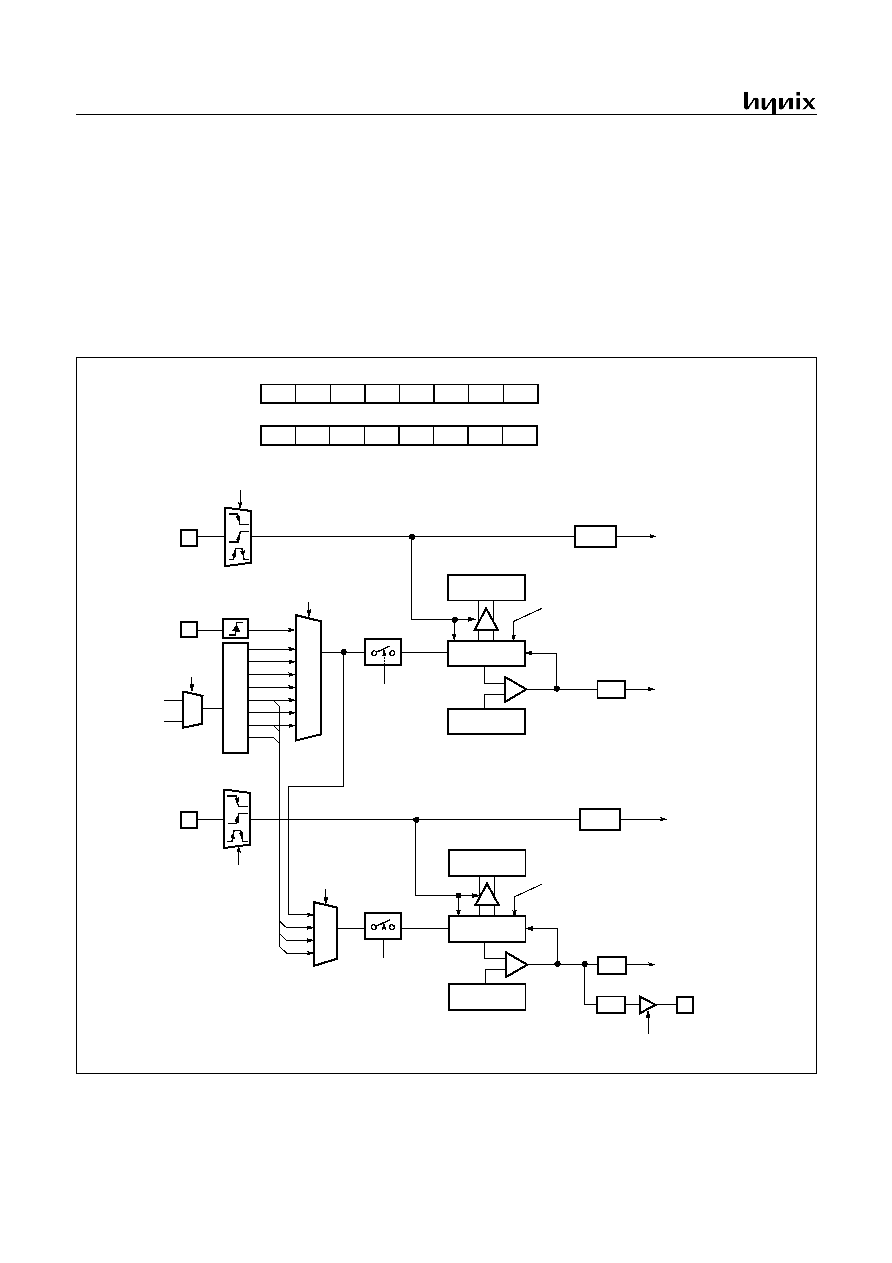
GMS81C7008/7016
52
APR., 2001 Ver 2.01
13.3 8-bit Capture Mode
The capture mode can be used to measure the pulse width be-
tween two edges. The Timer 0 capture mode is set by bit CAP0
of Timer Mode Register TM0, and the Timer 1 capture mode is
set by CAP1 of Timer Mode Register TM1 as shown in Figure
13-10. Timer 2 and Timer 3 have same architecture with Timer 0
and Timer 1.
The Timer/Counter register is incremented in response internal or
external input. This counting function is same with normal timer
mode, and Timer interrupt is generate when timer register T0 (T1,
T2, T3) increase and match TDR0 (TDR1, TDR2, TDR3).
Timer/Counter still does the above, but with the added feature
that a edge transition at external input INTn pin causes the current
.
Figure 13-10 8-bit Capture Mode (Timer0/Timer1 case)
f
timer
f
xin
2
prescaler value
TDR
1
+
(
)
×
×
--------------------------------------------------------------------------------
=
T0CK[2:0]
÷
2
÷
4
÷
8
MUX
000
001
010
÷
32
÷
128
÷
512
÷
2048
011
100
101
110
111
Edge Detector
EC0 PIN
T0CN
INT0IF
0: Stop
1: Clear and start
INT0
INTERRUPT
CDR0 (8-bit)
T0 (8-bit)
01
10
11
capture
IEDS[1:0]
CDR0 (8-bit)
CDR0
T0IF
TIMER 0
INTERRUPT
Comparator
COMPARE DATA
CDR0 (8-bit)
TDR0 (8-bit)
INT0 PIN
T0ST
clear
clear
T1CK[1:0]
÷
1
÷
2
÷
8
MUX
00
01
10
11
T1CN
0: Stop
1: Clear and start
CDR0 (8-bit)
T1 (8-bit)
CDR0 (8-bit)
CDR1
T1IF
TIMER 1
INTERRUPT
Comparator
COMPARE DATA
CDR0 (8-bit)
TDR1 (8-bit)
T1ST
clear
INT1IF
INT1
INTERRUPT
01
10
11
capture
IEDS[3:2]
INT1 PIN
clear
7
6
5
4
3
2
1
0
INITIAL VALUE: 00
H
ADDRESS: 0E0
H
TM0
X
X
X
X
X
X
1
X
TM1
BTCL
X
0
0
1
X
X
X
X
POL0
PWME0
T1CK1
INITIAL VALUE: 00
H
ADDRESS: 0E2
H
T1CK0 T1CN T1ST
16BIT0
CAP1
BTCL
-
CAP0
T0CK1 T0CK0 T0CN T0ST
-
T0CK2
÷
1
Pre
scaler
f
XIN
f
SXIN
0X
1X
SCMR[1:0]
R31/T1O/PWM0
F/F
PIN
PMR.6
[0D9
H
.6]
f
EX
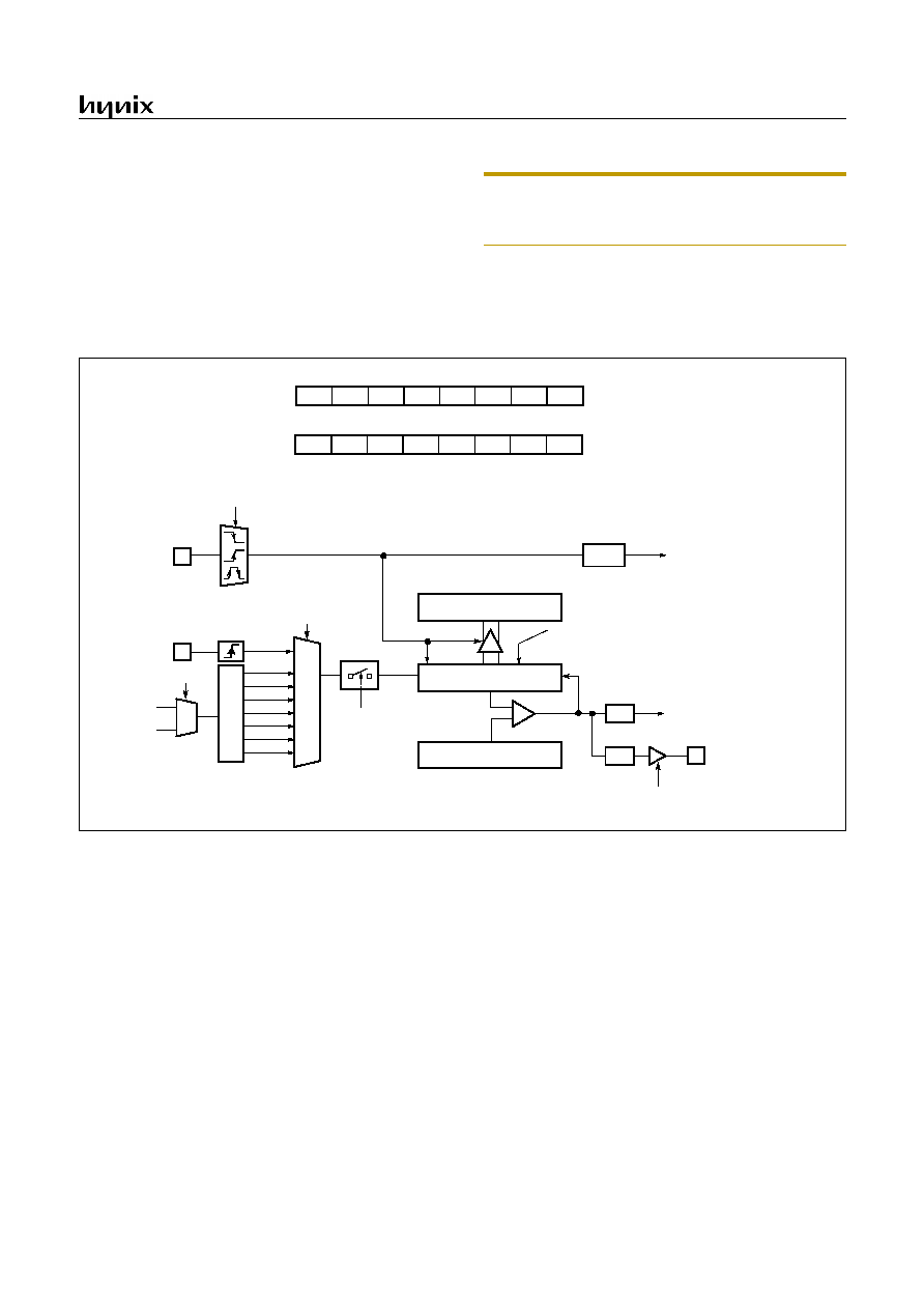
GMS81C7008/7016
APR., 2001 Ver 2.01
53
value in the Timer counter register (T0,T1), to be captured and
stored into registers CDRn (CDR0, CDR1), respectively. After
capture, the Timer counter register is cleared and restarts by hard-
ware. At this time, reading the address E1
H
as a CDR0, not T0.
T0, TDR0, CDR0 are located at same address. The other
CDR1~CDR3 are same. Refer to Timer registers of page 27.
It has three transition modes: "falling edge", "rising edge", "both
edge" which are selected by interrupt edge selection register
IEDS. Refer to "17.4 External Interrupt" on page 68. In addition,
the transition at INTn pin generate an interrupt.
Note: The CDRn and Tn are in same address.In the cap-
ture mode, reading operation is read as CDRn, not Tn be-
cause addressing path is opened to the CDRn.
Figure 13-11 16-bit Capture Mode
13.4 16-bit Capture Mode
16-bit capture mode is the same as 8-bit capture, except that the
Timer register is being run will 16 bits. Configuration is shown in
Figure 13-11.
13.5 Timer output port mode
The GMS81C7008/16 has a function of Timer compare output.
To pulse out, the timer match can goes out to port pin (T1O, T3O)
as shown in Figure 13-3, Figure 13-4 and Figure 13-9.
Thus pulse out is generated by the timer match. These operation
is implemented to pin T1O, T3O. This pin output the signal hav-
ing 50% duty square wave and output frequency is same as below
equation.
To use this function, the bit 6 and bit 7 of Port Mode Register
(PMR) are set or clear properly. In addition, 16-bit Timer output
mode is available, also
T0CK[2:0]
÷
2
÷
4
÷
8
MUX
000
001
010
÷
32
÷
128
÷
512
÷
2048
011
100
101
110
111
Edge Detector
EC0 PIN
T0CN
INT0IF
0: Stop
1: Clear and start
INT0
INTERRUPT
01
10
11
capture
IEDS[1:0]
T0IF
TIMER 0
INTERRUPT
Comparator
COMPARE DATA
INT0 PIN
T0ST
clear
clear
Pr
esca
ler
f
XIN
f
SXIN
0X
1X
SCMR[1:0]
R31/T1O/PWM0
F/F
PIN
PMR.6
CDR1
CDR0
TDR1
TDR0
T1
T0
BTCL
7
6
5
4
3
2
1
0
-
CAP0
T0CK1
INITIAL VALUE: 00
H
ADDRESS: 0E0
H
TM0
T0CK0 T0CN T0ST
-
T0CK2
X
X
X means don't care
1
BTCL
POL0
PWME0
T1CK1
INITIAL VALUE: 00
H
ADDRESS: 0E2
H
TM1
T1CK0 T1CN T1ST
16BIT0
CAP1
X
1
0
1
1
1
X
X
X
X
X
X
X
[0D9
H
.6]
16 BITS
MSB
LSB
f
EX
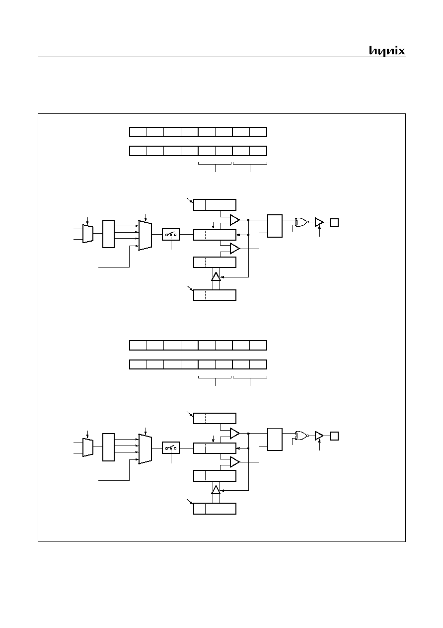
GMS81C7008/7016
54
APR., 2001 Ver 2.01
13.6 PWM Mode
The GMS81C70xx and GMS81C71xx have two high speed
PWM (Pulse Width Modulation) functions which shared with
Timer 1 and Timer 3.
Figure 13-12 PWM Mode
T1CK[1:0]
MUX
÷
8
÷
2
÷
1
11
10
01
00
T1CN
T1PPR (8-bit)
S
Comparator
clear
T1ST
7
6
5
4
3
2
1
0
TM1
BTCL
X
0
1
0
X
X
X
X
POL0
PWME0
T1CK1
INITIAL VALUE: 00
H
ADDRESS: 0E2
H
T1CK0 T1CN T1ST
16BIT0
CAP1
Pr
esca
ler
f
XIN
f
SXIN
0X
1X
SCMR[1:0]
2 Bit
T1 (8-bit)
(note1)
T1PDR (8-bit)
2 Bit
R
Q
T1PDR (8-bit)
2 Bit
T0 clock source
(from Timer 0)
POL0
R31/T1O/PWM0
PIN
PMR.6
PWM0HR
-
-
-
-
X
X
X
X
-
PWM02
INITIAL VALUE: 00
H
ADDRESS: 0E5
H
PWM03
-
PWM00
PWM01
-
-
Duty high
Period high
PWM[01:00]
[0E4
H
]
[0E5
H
]
PWM[03:02]
[0E3
H
]
[0E5
H
]
[0D9
H
.6]
2 Bit
Note1: In the PWM mode, 2 bits are added
by hardware automatically.
T3CK[1:0]
MUX
÷
8
÷
2
÷
1
11
10
01
00
T3CN
T3PPR (8-bit)
S
Comparator
clear
T3ST
7
6
5
4
3
2
1
0
TM3
BTCL
X
0
1
0
X
X
X
X
POL1
PWME1
T3CK1
INITIAL VALUE: 00
H
ADDRESS: 0E8
H
T3CK0 T3CN T3ST
16BIT1
CAP3
P
r
esca
ler
f
XIN
f
SXIN
0X
1X
SCMR[1:0]
2 Bit
T3 (8-bit)
(note1)
T3PDR (8-bit)
2 Bit
R
Q
T3PDR (8-bit)
2 Bit
T2 clock source
(from Timer 2)
POL1
R32/T3O/PWM1
PIN
PMR.7
PWM1HR
-
-
-
-
X
X
X
X
-
PWM12
INITIAL VALUE: 00
H
ADDRESS: 0EB
H
PWM13
-
PWM10
PWM11
-
-
Duty high
Period high
PWM[11:10]
[0EA
H
]
[0EB
H
]
PWM[13:12]
[0E9
H
]
[0EB
H
]
[0D9
H
.7]
2 Bit
f
EX
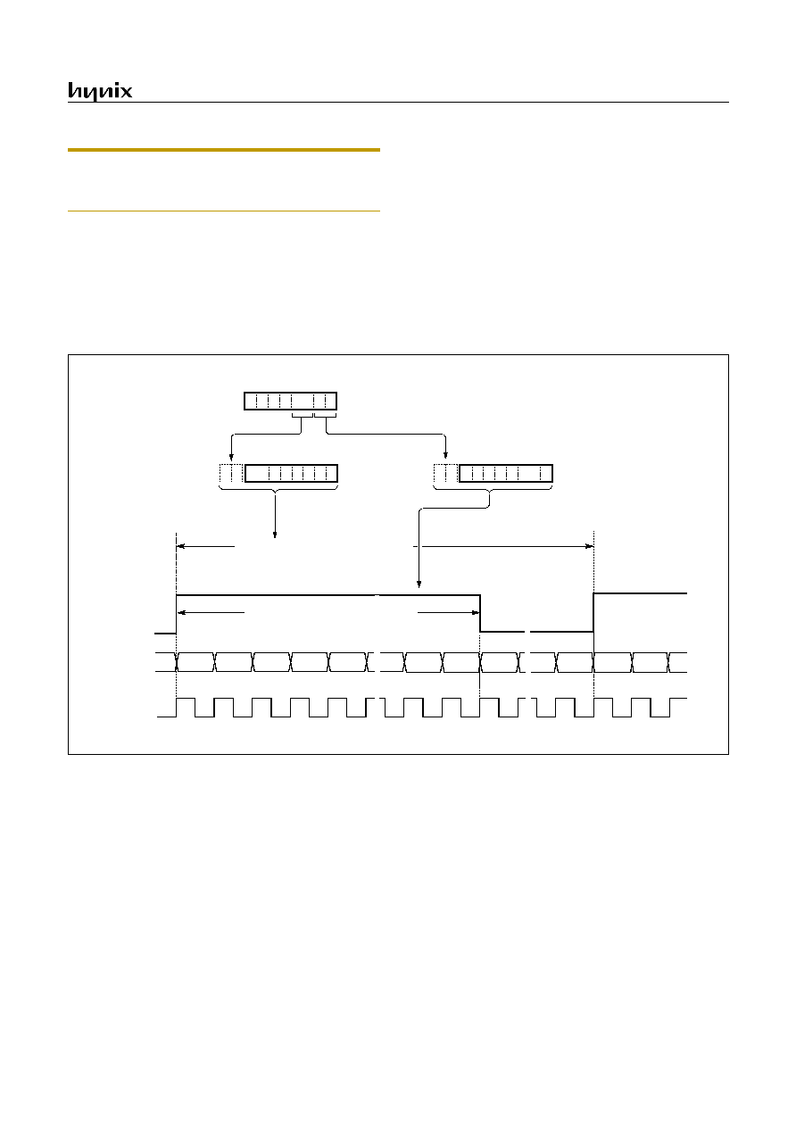
GMS81C7008/7016
APR., 2001 Ver 2.01
55
Note: Whenever change the register content of Period or
Duty of PWM output, the timer counter Tn must be stopped
and restart again by software.
The PWM0 will be explained in this chapter. Other PWM1 has
same architecture. Pin R32/T1O/PWM0 outputs up to a 10-bit
resolution PWM output. This pin should be configure as a PWM
output to set bit PRM0.6 to "1".
The period of the PWM output is determined by the T1PPR
(PWM0 Period Register) and PWM0HR[3:2] and the duty is de-
t e r mi n ed b y t h e T 1 P D R ( P W M 0 D u t y R e g i s t e r ) a n d
PWM0HR[1:0].
The user writes the lower 8-bit period value to the T1PPR and the
higher 2-bit period value to the PWM0HR[3:2].
And writes duty value to the T1PDR and the PWM0HR[1:0]
same way.
The T1PDR is configure as a double buffering for glitchless
PWM output. In, the duty data is transferred from the master to
the slave when the period data matched to the counted value. (i.e.
at the beginning of next duty cycle)
The relation between frequency and resolution is in inverse pro-
portion. Table 13-1 shows the PWM frequency in each clock
source. If it needed higher frequency of PWM, it should be re-
duced resolution.
Figure 13-13 Example of Register setting
The bit POL0 of TM0 decides the polarity of duty cycle.
If the duty value is set same to the period value, the PWM output
is determined by the bit POL0 (1: High, 0: Low). And if the duty
value is set to "00
H
", the PWM output is determined by the bit
POL0 (1: Low, 0: High).
It can be changed duty value when the PWM output. However the
changed duty value is output after the current period is over. And
it can be maintained the duty value at present output when
changed only period value shown as Figure 13-14. As it were, the
absolute duty time is not changed in varying frequency. But the
changed period value must greater than the duty value.
At PWM output start command, one first pulse would be output
abnormally. Because if user writes register values while timer is
in operation, these register could be set with certain values at first.
To prevent this operation, user must stop PWM timer clock and
then set the duty and the period register values.
T1
~~
~~
01
H
02
H
03
H
04
H
256
H
257
H
258
H
3E7
H
01
H
~~
~~
~~
PWM output
Duty; (257
H
+1) x 500nS = 300uS
00
H
00
H
~~
~~
02
H
Clock source
Period; (3E7
H
+1) x 500nS = 500uS
T1PPR
PWM0HR
1 1
1 1 1 0 0 1 1 1
T1PDR
1 0
0 1 0 1 0 1 1 1
[0E4
H
]
[0E3
H
]
[0E5
H
]
- - - - 1 1 1 0
Period
Duty
~~
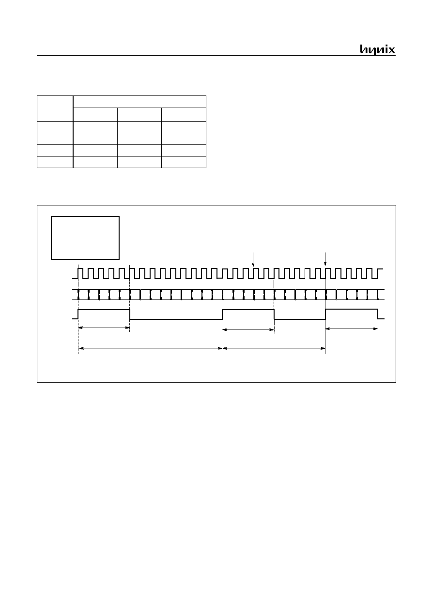
GMS81C7008/7016
56
APR., 2001 Ver 2.01
Example:
Timer1 = 2kHz, 30% duty PWM mode
LDM
TM1,#00H
LDM
T1PPR,#0E8H
LDM
T1PDR,#58H
LDM
PWM0HR,0000_1110B
LDM
TM1,#1010_1011B
Refer to Figure 13-13.
Figure 13-14 Example of changing the period in absolute duty cycle at 4MHz
Resolutio
n
PWM clock source
f
XIN
÷
÷
÷
÷
1
f
XIN
÷
÷
÷
÷
2
f
XIN
÷
÷
÷
÷
1024
10-bit
3.9kHz
1.95kHz
3.8Hz
9-bit
7.8kHz
3.9kHz
7.6Hz
8-bit
15.6kHz
7.8kHz
15.3Hz
7-bit
31.2kHz
15.6kHz
30.5Hz
Table 13-1 PWM Frequency vs. Resolution at 4MHz
Source
T1
PWM
POL=1
Duty Cycle
Period Cycle [ (D
H
+1) x 2uS = 28uS, 35.7kHz ]
PWMHR = 00
H
T1PPR = 0D
H
T1PDR = 04
H
T1CK[1:0] = 10 (2uS)
00 01 02
03
04
05
07
08
0A 0B 0C 0D 00
01
02
03
04
05 06
07
08
09
00
01
02 03
06
09
04
[ (4+1) x 2uS = 10uS ]
Duty Cycle
[ (4+1) x 2uS =10uS ]
Period Cycle [ (9+1) x 2uS = 20uS, 50kHz ]
Duty Cycle
[ (4+1) x 2uS = 10uS ]
Write "09
H
" to T1PPR
Period changed
clock
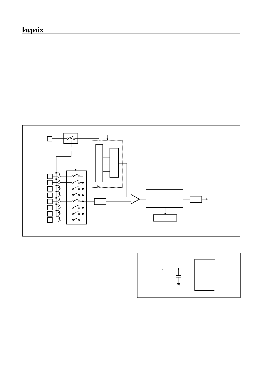
GMS81C7008/7016
APR., 2001 Ver 2.01
57
14. ANALOG DIGITAL CONVERTER
The analog-to-digital converter (A/D) allows conversion of an
analog input signal to a corresponding 8-bit digital value. The A/
D module has eight analog inputs, which are multiplexed into one
sample and hold. The output of the sample and hold is the input
into the converter, which generates the result via successive ap-
proximation. The analog supply voltage is connected to AV
DD
of
ladder resistance of A/D module.
The A/D module has two registers which are the control register
ADCM and A/D result register ADR. The register ADCM, shown
in Figure 14-4, controls the operation of the A/D converter mod-
ule. The port pins can be configured as analog inputs or digital I/
O. To use analog inputs, I/O is selected input mode by R2DD di-
rection register.
How to Use A/D Converter
The processing of conversion is start when the start bit ADST is
set to "1". After one cycle, it is cleared by hardware. The register
ADR contains the results of the A/D conversion. When the con-
version is completed, the result is loaded into the ADR, the A/D
conversion status bit ADSF is set to "1", and the A/D interrupt
flag AIF is set. The block diagram of the A/D module is shown in
Figure 14-1. The A/D status bit ADSF is set automatically when
A/D conversion is completed, cleared when A/D conversion is in
process. The conversion time takes maximum 20 uS (at f
XIN
=4
MHz).
Figure 14-1 A/D Block Diagram
A/D Converter Cautions
(1) Input voltage range of AN0 to AN7
The input voltage of AN0 to AN7 should be within the specifica-
tion range. In particular, if a voltage above AV
DD
or below AV
SS
is input (even if within the absolute maximum rating range), the
conversion value for that channel can not be indeterminate. The
conversion values of the other channels may also be affected.
(2) Noise countermeasures
In order to maintain 8-bit resolution, attention must be paid to
noise on pins AV
DD
and AN0 to AN7. Since the effect increases
in proportion to the output impedance of the analog input source,
it is recommended that a capacitor be connected externally as
shown in Figure 14-2 in order to reduce noise.
.
Figure 14-2 Analog Input Pin Connecting Capacitor
R20/AN0
R21/AN1
R22/AN2
R23/AN3
R24/AN4
R25/AN5
R26/AN6
R27/AN7
S/H
Sample & Hold
"0"
"1"
ADEN
AV
DD
8-
bi
t D
A
C
L
A
DDER RESIST
OR
ADIF
A/D
INTERRUPT
SUCCESSIVE
APPROXIMATION
CIRCUIT
ADR
A/D result register
ADDRESS: ED
H
RESET VALUE: Undefined
000
001
010
011
100
101
110
111
ADS[2:0]
AN0~AN7
100~1000pF
Analog
Input
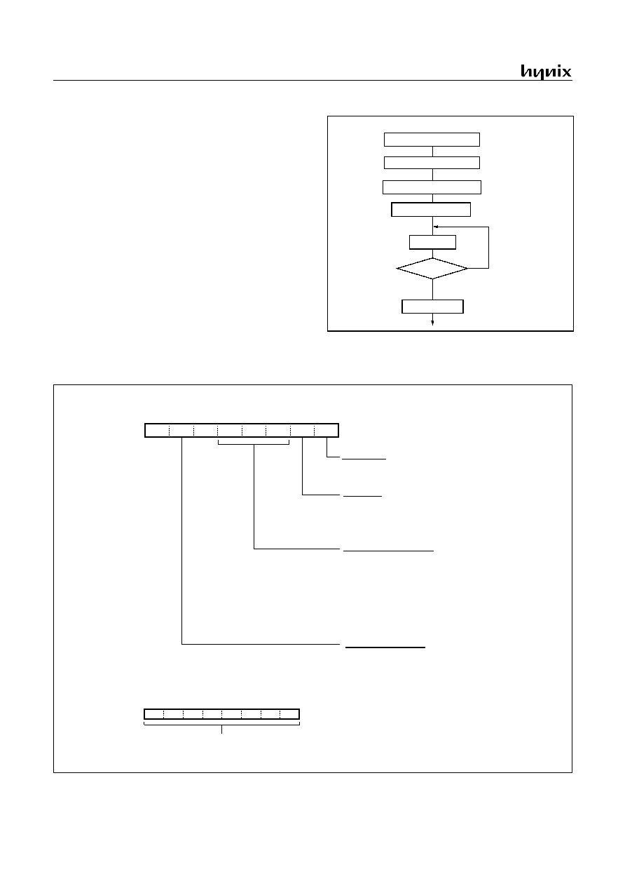
GMS81C7008/7016
58
APR., 2001 Ver 2.01
(3) AD pin sharing with normal I/O port
The analog input pins AN0 to AN7 also function as input/output
port (PORT R20~R27) pins. When A/D conversion is performed
with any of pins AN0 to AN7 selected, be sure not to execute a
PORT input instruction while conversion is in progress, as this
may reduce the conversion resolution.
Also, if digital pulses are applied to a pin adjacent to the pin in the
process of A/D conversion, the expected A/D conversion value
may not be obtainable due to coupling noise. Therefore, avoid ap-
plying pulses to pins adjacent to the pin undergoing A/D conver-
sion.
(4) AV
DD
pin input impedance
A series resistor string of approximately 10k
is connected be-
tween the AV
DD
pin and the AV
SS
pin.
Therefore, if the output impedance of the reference voltage
source is high, this will result in parallel connection to the series
resistor string between the AV
DD
pin and the AV
SS
pin, and there
will be a large reference voltage error.
Figure 14-3 A/D converter Operation Flow
Figure 14-4 A/D Converter Control Register
ENABLE A/D CONVERTER
A/D START ( ADST = 1 )
NOP
ADSF = 1
A/D INPUT CHANNEL SELECT
ANALOG REFERENCE SELECT
READ ADR
YES
NO
BTCL
7
6
5
4
3
2
1
0
ADEN
-
ADST
A/D status bit
Analog input channel select
INITIAL VALUE: -0-0 0001
B
ADDRESS: 0EC
H
ADCM
ADSF
A/D converter Enable bit
0: A/D converter module turn off and
current is not flow.
1: Enable A/D converter
R/W
R/W
R/W
R/W
R/W
R
000: Channel 0 (AN0)
001: Channel 1 (AN1)
010: Channel 2 (AN2)
011: Channel 3 (AN3)
100: Channel 4 (AN4)
101: Channel 5 (AN5)
110: Channel 6 (AN6)
111: Channel 7 (AN7)
0: A/D conversion is in progress
1: A/D conversion is completed
A/D start bit
Setting this bit starts an A/D conversion.
After one cycle, bit is cleared to "0" by hardware.
ADS1 ADS0
-
ADS2
INITIAL VALUE: Undefined
ADDRESS: 0ED
H
ADR
A/D Conversion Data
BTCL
7
6
5
4
3
2
1
0
R
R
R
R
R
R
R
R
0: -
1: A/D start
-
-
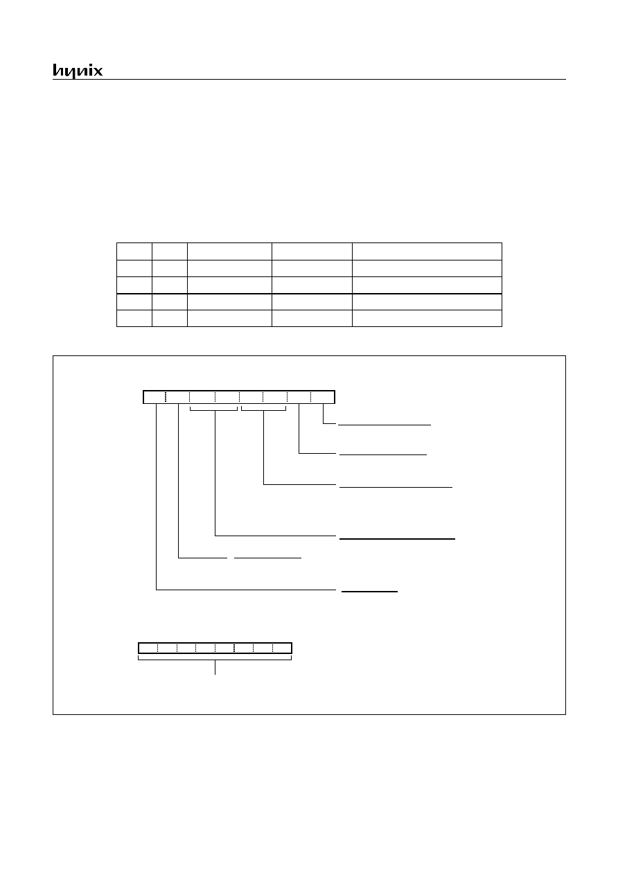
GMS81C7008/7016
APR., 2001 Ver 2.01
59
15. SERIAL COMMUNICATION
The serial interface is used to transmit/receive 8-bit data serially.
Serial communication block consists of serial I/O data register,
serial I/O mode register, clock selection circuit, octal counter and
control circuit as illustrated in Figure 15-1.Pin R07/SIN, R06/
SOUT and R05/SCLK pins are controlled by the Serial Mode
Register. The contents of the Serial I/O data register can be writ-
ten into or read out by software.
The serial communication is activated by the instruction "SET1
SIOST". The octal counter is reset to "0" by this instruction, starts
counting at the falling or rising edge (by POL selection) of the
transmit clock (SCLK), and it increments at the every clock. A se-
rial interrupt request flag is set when the eighth transmit clock
signal is input (the serial interface is reset) or when serial commu-
nication is discontinued (the octal counter is reset).
The data in the Serial Data Register can be shifted synchronously
with the transfer clock signal.
Figure 15-1 SCI Control Register
SCK1
SCK0
SCLK/R05 Port
Clock Source
Prescaler Divide Ratio
0
0
SCLK output
Internal clock
÷
4
0
1
SCLK output
Internal clock
÷
16
1
0
SCLK output
Internal clock
Use clock from Timer 0 overflow
1
1
SCLK input
External clock
-
BTCL
7
6
5
4
3
2
1
0
MSB
POL
SIOST
Serial transmission status bit
Serial transmission Clock selection
INITIAL VALUE: 0000_0001
B
ADDRESS: 0FE
H
SIOM
SIOSF
MSB first or LSB first
0: LSB First
1: MSB First
R/W
R/W
R/W
R/W
R/W
R
00: f
XIN
÷
4
01: f
XIN
÷
16
10: Timer 0 Overflow
11: External Clock
0: Serial transmission is in progress
1: Serial transmission is completed
Serial transmission start bit
Setting this bit starts an Serial transmission.
After one cycle, bit is cleared to "0" by hardware.
SCK1 SCK0
SIO1
SIO0
R/W
Serial transmission Operation Mode
00: Normal Port(R05,R06,R07)
01: Sending Mode(SCLK,SOUT,R07)
10: Receiving Mode(SCLK,R06,SIN)
11: Sending & Receiving Mode(SCLK,SOUT,SIN)
INITIAL VALUE: Undefined
ADDRESS: 0FF
H
SIOR
BTCL
7
6
5
4
3
2
1
0
R/W R/W R/W R/W
R/W R/W
R/W
R/W
Sending Data during Sending Mode
Receiving Data during Receiving Mode
Selection Polarity
0: Data in on rising edge, data out on falling edge
1: Data in on falling edge, data out on rising edge
R/W
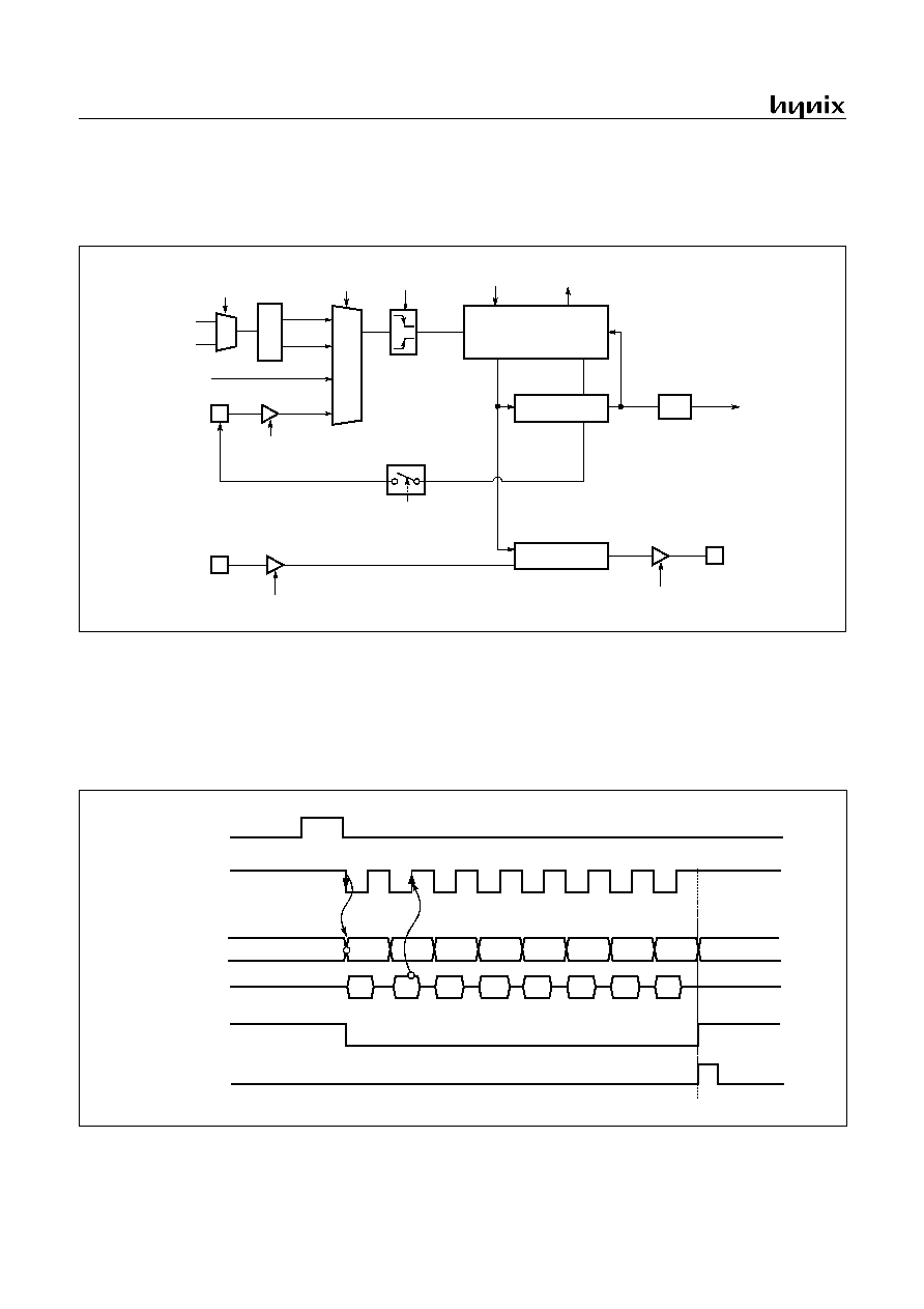
GMS81C7008/7016
60
APR., 2001 Ver 2.01
Serial I/O Mode Register(SIOM) controls serial I/O function.
The POL bit control which edge
According to SCK1 and SCK0, the internal clock or external
clock can be selected.
Serial I/O Data Register(SIOR) is an 8-bit shift register.
Figure 15-2 Block Diagram of SCI
15.1 Transmission/Receiving Timing
The serial transmission is started by setting SIOST(bit1 of
SIOM) to "1". After one cycle of SCK, SIOST is cleared
automatically to "0". The serial output data from 8-bit shift
register is output at falling edge of SCLK. And input data
is latched at rising edge of SCLK pin. When transmission
clock is counted 8 times, serial I/O counter is cleared as
`0". Transmission clock is halted in "H" state and serial I/
O interrupt(SIOIF) occurred.
Figure 15-3 SPI Timing Diagram at POL=0
R05/SCLK PIN
CONTROL CIRCUIT
R06/SOUT PIN
Serial IO Data
Octal Counter
Serial communication
Interrupt
SIOIF
R07/SIN PIN
SCK, SIO
overflow
SCK[1:0]
MUX
÷
16
÷
4
11
10
01
00
Pr
esca
ler
f
XIN
f
SXIN
0X
1X
SCMR[1:0]
T0OV
(Timer 0 overflow)
POL
SIOST
start
SIOSF
complete
clock
clear
SIO1
SIO0
[0FF
H
]
Edge Detector
SIO[1:0]
shift clock
SCLK OUT
D1
D2
D3
D4
D6
D7
D0
D5
D 1
D 2
D 3
D 4
D 6
D 7
D 0
D 5
SIOST
SCLK [R05]
(POL=0)
SOUT [R06]
SIN [R07]
SIOIF
(Interrupt Req.)
SIOSF
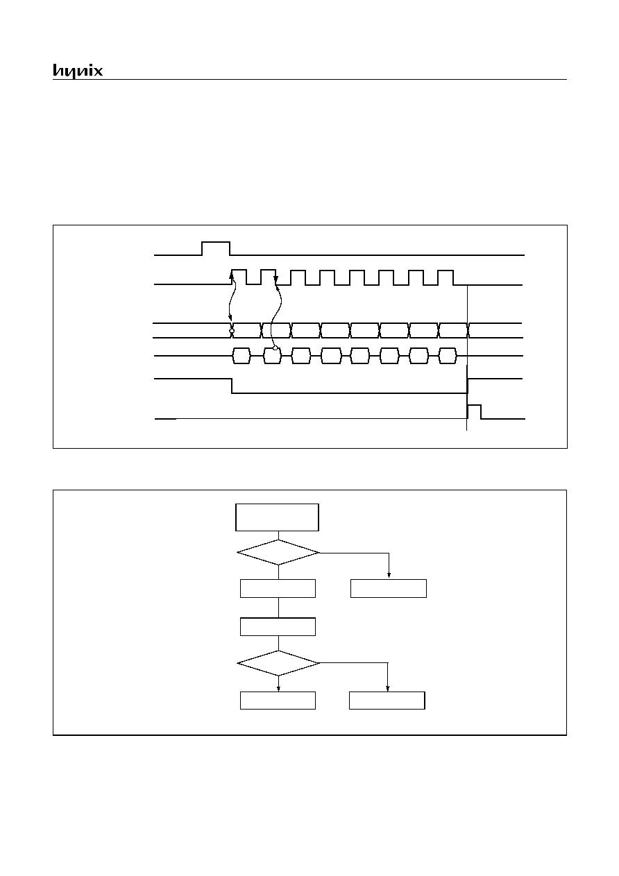
GMS81C7008/7016
APR., 2001 Ver 2.01
61
15.2 The method of Serial I/O
1. Select transmission/receiving mode
When external clock is used, the frequency should be less than
1MHz and recommended duty is 50%.
2. In case of sending mode, write data to be send to SIOR.
3. Set SIOST to "1" to start serial transmission.
If both transmission mode is selected and transmission is per-
formed simultaneously it would be made error.
4. The SIO interrupt is generated at the completion of SIO and
SIOSF is set to "1". In SIO interrupt service routine, correct trans-
mission should be tested.
5. In case of receiving mode, the received data is acquired by
reading the SIOR.
Figure 15-4 SPI Timing Diagram at POL=1
15.3 The Method to Test Correct Transmission
Figure 15-5 Serial Method to Test Transmission
D1
D2
D3
D4
D6
D7
D0
D5
D 1
D 2
D 3
D 4
D 6
D 7
D 0
D 5
SIOST
SCLK [R05]
(POL=1)
SOUT [R06]
SIN [R07]
SCIIF
SIOSF
Serial I/O Interrupt
Service Routine
SE = 0
Write SIOM
Normal Operation
Overrun Error
Abnormal
SIOSF
0
1
- SE : Interrupt Enable Register Low IENL(Bit3)
- SR : Interrupt Request Flag Register Low IRQL(Bit3)
SR
0
1
GMS81C7008/7016
62
APR., 2001 Ver 2.01
16. BUZZER FUNCTION
The buzzer driver block consists of 6-bit binary counter, buzzer
register, and clock source selector. It generates square-wave
which has very wide range frequency (500Hz ~ 250kHz at f
XIN
=
4MHz) by user software.
A 50% duty pulse can be output to R30/BUZ pin to use for piezo-
electric buzzer drive. Pin R30 is assigned for output port of Buzz-
er driver by setting the bit 5 of PMR (address D9
H
) to "1". At this
time, the pin R30 must be defined as output mode (the bit 0 of
R3DD=1).
Example: 2.4kHz output at 4MHz.
LDM
R3DD,#XXXX_XXX1B
LDM
BUR,#0111_0011B
SET1
PMR.5
;BUZ ON
CLR1
PMR.5
;BUZ OFF
X means don't care
The bit 0 to 5 of BUR determines output frequency for buzzer
driving.
Equation of frequency calculation is shown below.
f
BUZ
: Buzzer frequency
f
XIN
: Oscillator frequency
Divide Ratio: Prescaler divide ratio by BUCK[1:0]
BUR: Lower 6-bit value of BUR. Buzzer period value.
The frequency of output signal is controlled by the buzzer control
register BUR.The BUR[5:0] determine output frequency for
buzzer driving.
Figure 16-1 Block Diagram of Buzzer Driver
Figure 16-2 PMR and Buzzer Register
f
BUZ
f
XIN
2
DivideRatio
BUR 5:0
[
]
1
+
(
)
×
×
----------------------------------------------------------------------------------------
=
P
r
esca
ler
÷
8
÷
32
÷
16
÷
64
R30/BUZ PIN
PMR.5
R30 port data
0
1
F/F
÷
2
Comparator
6-bit Compare Data
6-bit Binary Counter
MUX
00
01
10
11
BUR[5:0]
[0FD
H
]
BUR[7:6]
f
XIN
f
SXIN
0X
1X
SCMR[1:0]
BUR[5:0]
BUR
ADDRESS: 0FD
H
RESET VALUE: Undefined
W
W
W
W
W
W
Source clock select
00:
÷
8
01:
÷
16
10:
÷
32
11:
÷
64
Define Frequency of Buzzer signal
W
W
BUCK1 BUCK0
R30/BUZ Selection
PMR
ADDRESS: 0D9
H
RESET VALUE: 00
H
R/W R/W R/W R/W R/W R/W
0: R30 port (Turn off buzzer)
R/W R/W
PWM1
BUZ
PWM0
INT0
INT1
INT2
EC0
EC2
1: BUZ port (Turn on buzzer)
GMS81C7008/7016
APR., 2001 Ver 2.01
63
Note that BUR is a write-only register.
The 6-bit counter is cleared and starts the counting by writing sig-
nal at BUR register. It is incremental from 00
H
until it matches 6-
bit BUR value.
When main-frequency is 4MHz, buzzer frequency is shown as
below table. The unit is kHz.
BUR
[5:0]
BUCK[1:0]
BUR
[5:0]
BUCK[1:0]
00
01
10
11
00
01
10
11
00
01
02
03
04
05
06
07
250.000
125.000
83.333
62.500
50.000
41.667
35.714
31.250
125.000
62.500
41.667
31.250
25.000
20.833
17.857
15.625
62.500
31.250
20.833
15.625
12.500
10.417
8.929
7.813
31.250
15.625
10.417
7.813
6.250
5.208
4.464
3.906
20
21
22
23
24
25
26
27
7.576
7.353
7.143
6.944
6.757
6.579
6.410
6.250
3.788
3.676
3.571
3.472
3.378
3.289
3.205
3.125
1.894
1.838
1.786
1.736
1.689
1.645
1.603
1.563
0.947
0.919
0.893
0.868
0.845
0.822
0.801
0.781
08
09
0A
0B
0C
0D
0E
0F
27.778
25.000
22.727
20.833
19.231
17.857
16.667
15.625
13.889
12.500
11.364
10.417
9.615
8.929
8.333
7.813
6.944
6.250
5.682
5.208
4.808
4.464
4.167
3.906
3.472
3.125
2.841
2.604
2.404
2.232
2.083
1.953
28
29
2A
2B
2C
2D
2E
2F
6.098
5.952
5.814
5.682
5.556
5.435
5.319
5.208
3.049
2.976
2.907
2.841
2.778
2.717
2.660
2.604
1.524
1.488
1.453
1.420
1.389
1.359
1.330
1.302
0.762
0.744
0.727
0.710
0.694
0.679
0.665
0.651
10
11
12
13
14
15
16
17
14.706
13.889
13.158
12.500
11.905
11.364
10.870
10.417
7.353
6.944
6.579
6.250
5.952
5.682
5.435
5.208
3.676
3.472
3.289
3.125
2.976
2.841
2.717
2.604
1.838
1.736
1.645
1.563
1.488
1.420
1.359
1.302
30
31
32
33
34
35
36
37
5.102
5.000
4.902
4.808
4.717
4.630
4.545
4.464
2.551
2.500
2.451
2.404
2.358
2.315
2.273
2.232
1.276
1.250
1.225
1.202
1.179
1.157
1.136
1.116
0.638
0.625
0.613
0.601
0.590
0.579
0.568
0.558
18
19
1A
1B
1C
1D
1E
1F
10.000
9.615
9.259
8.929
8.621
8.333
8.065
7.813
5.000
4.808
4.630
4.464
4.310
4.167
4.032
3.906
2.500
2.404
2.315
2.232
2.155
2.083
2.016
1.953
1.250
1.202
1.157
1.116
1.078
1.042
1.008
0.977
38
39
3A
3B
3C
3D
3E
3F
4.386
4.310
4.237
4.167
4.098
4.032
3.968
3.906
2.193
2.155
2.119
2.083
2.049
2.016
1.984
1.953
1.096
1.078
1.059
1.042
1.025
1.008
0.992
0.977
0.548
0.539
0.530
0.521
0.512
0.504
0.496
0.488
Table 16-1 Buzzer Frequency at 4MHz
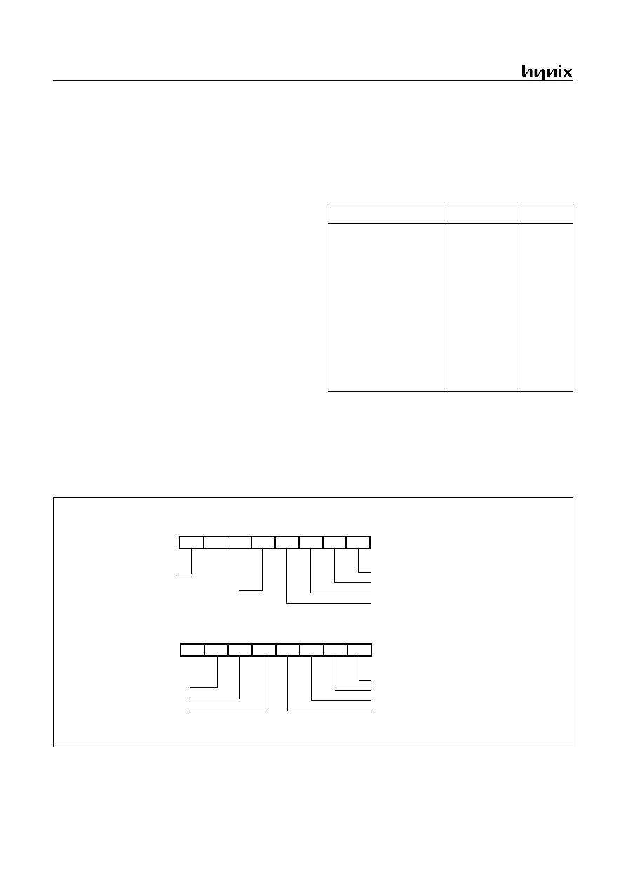
GMS81C7008/7016
64
APR., 2001 Ver 2.01
17. INTERRUPTS
The GMS81C7008/16 interrupt circuits consist of Interrupt en-
able register (IENH, IENL), Interrupt request flags of IRQH,
IRQL, Priority circuit, and Master enable flag ("I" flag of PSW).
Thirteen interrupt sources are provided. The configuration of in-
terrupt circuit is shown in Figure 17-2.
The keyscan interrupt is generated when 1-to-0 transition is de-
tected at KS0 or KS0 pin.
The Basic Interval Timer Interrupt is generated by BITIF which
is set by an overflow in the timer register.
The Watchdog timer Interrupt is generated by WDTIF which set
by a match in Watchdog timer register.
The External Interrupts INT0 ~ INT2 each can be transition-acti-
vated (1-to-0 or 0-to-1 transition) by selection IEDS.
The flags that actually generate these interrupts are bit INT0IF,
INT1IF and INT2IF in register IRQH and IRQL. When an exter-
nal interrupt is generated, the flag that generated it is cleared by
the hardware when the service routine is vectored to only if the
interrupt was transition-activated.
The Timer 0 ~ Timer 3 Interrupts are generated by T0IF~T3IF
which are set by a match in their respective timer/counter register.
The Serial Communication Interrupts are generated by SIOIF
which is set by 8-bit serial data transmitting or receiving through
SCK, SIN, SOUT pin.
The AD converter Interrupt is generated by ADIF which is set by
finishing the analog to digital conversion.
The Watch Timer Interrupt is generated by WTIF which is set by
an 14-bit binary counter overflow.
The interrupts are controlled by the interrupt master enable flag
I-flag (bit 2 of PSW on page 19), the interrupt enable register
(IENH, IENL), and the interrupt request flags (in IRQH and
IRQL) except Power-on reset and software BRK interrupt. Below
table shows the Interrupt priority.
Vector addresses are shown in Figure 8-6 on page 21. Interrupt
enable registers are shown in Figure 17-3. These registers are
composed of interrupt enable flags of each interrupt source and
these flags determines whether an interrupt will be accepted or
not. When enable flag is "0", a corresponding interrupt source is
prohibited. Note that PSW contains also a master enable bit, I-
flag, which disables all interrupts at once.
Figure 17-1 Interrupt Request Flag
Reset/Interrupt
Symbol
Priority
Hardware Reset
Key scan Interrupt
Basic Interval Timer
Watchdog Timer
External Interrupt 0
External Interrupt 1
Timer/Counter 0
Timer/Counter 1
External Interrupt 2
Serial Communication
ADC Interrupt
Watch Timer Interrupt
Timer/Counter 2
Timer/Counter 3
RESET
KS
BIT
WDT
INT0
INT1
Timer 0
Timer 1
INT2
SCI
ADC
WT
Timer 2
Timer 3
-
1
2
3
4
5
6
7
8
9
10
11
12
13
WDTIF
R/W
-
Timer/Counter 3
INITIAL VALUE: -000 0000
B
ADDRESS: 0DD
H
IRQH
KSIF
MSB
LSB
T0IF
T1IF
INT0IF INT1IF
BITIF
R/W
R/W
Timer/Counter 2
Timer/Counter 1 interrupt request flag
External interrupt 1
Serial Communication
INITIAL VALUE: 0--0 0000
B
ADDRESS: 0DC
H
IRQL
MSB
LSB
Timer/Counter 0
R/W
R/W
-
R/W
R/W
Basic Interval Timer
Watchdog timer
A/D Converter
External interrupt 0
Key scan
SIOIF
-
INT2IF
-
T2IF
T3IF
ADIF
WTIF
-
R/W
R/W
R/W
R/W
R/W
-
R/W
Watch timer
External interrupt 2
GMS81C7008/7016
APR., 2001 Ver 2.01
65
.
Figure 17-2 Block Diagram of Interrupt
Figure 17-3 Interrupt Enable Flag
INT1
INT0
INT2
INT2IF
IENL
Interrupt Enable
Interrupt Enable
IRQL [0DC
H
]
IRQH [0DD
H
]
Interrupt
Vector
Address
Generator
Internal bus line
Register (Higher byte)
Internal bus line
Register (Lower byte)
Release STOP
To CPU
Interrupt Master
Enable Flag
I-flag
IENH
P
r
io
r
i
ty Co
n
t
r
o
l
I-flag is in PSW, it is cleared by "DI", set by
"EI" instruction. When it goes interrupt service,
I-flag is cleared by hardware, thus any other
interrupt are inhibited. When interrupt service is
completed by "RETI" instruction, I-flag is set to
"1" by hardware.
[0DA
H
]
[0DB
H
]
INT0IF
INT1IF
T3IF
T2IF
Timer 3
Timer 2
A/D Converter
ADIF
SIOIF
BITIF
Watchdog Timer
Serial
BIT
WDTIF
Communication
Watch Timer
WTIF
Key Scan
KSIF
T1IF
T0IF
Timer 1
Timer 0
SIOE
INT2E
Timer/Counter 3 interrupt enable flag
INITIAL VALUE: 0--0 0000
B
ADDRESS: 0DA
H
IENL
-
MSB
LSB
T2E
T3E
ADE
WTE
-
R/W
R/W
Timer/Counter 2 interrupt enable flag
Watch Timer interrupt enable flag
Serial Communication interrupt enable flag
INITIAL VALUE: -000 0000
B
ADDRESS: 0DB
H
IENH
MSB
LSB
R/W
R/W
R/W
-
R/W
Basic Interval Timer interrupt enable flag
Watchdog timer interrupt enable flag
A/D Converter interrupt enable flag
External interrupt 2 enable flag
0: Disable
1: Enable
VALUE
WDTE
R/W
-
KSE
T0E
T1E
INT0E
INT1E
BITE
R/W
R/W
R/W
R/W
-
R/W
R/W
-
Timer/Counter 1 interrupt enable flag
Timer/Counter 0 interrupt enable flag
External interrupt 1 enable flag
External interrupt 0 enable flag
Key scan interrupt enable flag
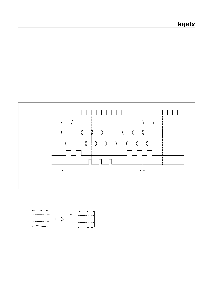
GMS81C7008/7016
66
APR., 2001 Ver 2.01
17.1 Interrupt Sequence
An interrupt request is held until the interrupt is accepted or the
interrupt latch is cleared to "0" by a reset or an instruction. Inter-
r u p t a c c e p t a n c e s e q u e n c e r e q u i r e s 8
f
X I N
( 2
µ
s a t
f
MAIN
=4.19MHz) after the completion of the current instruction
execution. The interrupt service task is terminated upon execu-
tion of an interrupt return instruction [RETI].
Interrupt acceptance
1. The interrupt master enable flag (I-flag) is cleared to
"0" to temporarily disable the acceptance of any follow-
ing maskable interrupts. When a non-maskable inter-
rupt is accepted, the acceptance of any following
interrupts is temporarily disabled.
2. Interrupt request flag for the interrupt source accepted is
cleared to "0".
3. The contents of the program counter (return address)
and the program status word are saved (pushed) onto the
stack area. The stack pointer decreases 3 times.
4. The entry address of the interrupt service program is
read from the vector table address and the entry address
is loaded to the program counter.
5. The instruction stored at the entry address of the inter-
rupt service program is executed.
Figure 17-4 Timing chart of Interrupt Acceptance and Interrupt Return Instruction
A interrupt request is not accepted until the I-flag is set to "1"
even if a requested interrupt has higher priority than that of the
current interrupt being serviced.
When nested interrupt service is required, the I-flag should be set
to "1" by "EI" instruction in the interrupt service program. In this
case, acceptable interrupt sources are selectively enabled by the
individual interrupt enable flags.
Saving/Restoring General-purpose Register
During interrupt acceptance processing, the program counter and
the program status word are automatically saved on the stack, but
accumulator and other registers are not saved itself. These regis-
ters are saved by the software if necessary. Also, when multiple
interrupt services are nested, it is necessary to avoid using the
same data memory area for saving registers.
The following method is used to save/restore the general-purpose
registers.
V.L.
System clock
Address Bus
PC
SP
SP-1
SP-2
V.H.
New PC
V.L.
Data Bus
Not used
PCH
PCL
PSW
ADL
OP code
ADH
Instruction Fetch
Internal Read
Internal Write
Interrupt Processing Step
Interrupt Service Task
V.L. and V.H. are vector addresses.
ADL and ADH are start addresses of interrupt service routine as vector contents.
Watch Timer
012
H
0E3
H
0FFE4
H
0FFE5
H
0E
H
2E
H
0E312
H
0E313
H
Entry Address
Correspondence between vector table address for Watch Timer Interrupt
and the entry address of the interrupt service program.
Vector Table Address
GMS81C7008/7016
APR., 2001 Ver 2.01
67
Example: Register save using push and pop instructions
General-purpose register save/restore using push and pop instruc-
tions;
17.2 BRK Interrupt
Software interrupt can be invoked by BRK instruction, which has
the lowest priority order.
Interrupt vector address of BRK is shared with the vector of
TCALL 0 (Refer to Program Memory Section). When BRK inter-
rupt is generated, B-flag of PSW is set to distinguish BRK from
TCALL 0.
Each processing step is determined by B-flag as shown in Figure
17-5.
Figure 17-5 Execution of BRK/TCALL0
17.3 Multi Interrupt
If two requests of different priority levels are received simulta-
neously, the request of higher priority level is serviced. If re-
qu est s of th e int errup t are received at t he same t ime
simultaneously, an internal polling sequence determines by hard-
ware which request is serviced.
However, multiple processing through software for special fea-
tures is possible. Generally when an interrupt is accepted, the I-
flag is cleared to disable any further interrupt. But as user sets I-
flag in interrupt routine, some further interrupt can be serviced
even if certain interrupt is in progress.
Example: During Timer1 interrupt is in progress, INT0 interrupt
serviced without any suspend.
TIMER1:
PUSH
A
PUSH
X
PUSH
Y
LDM
IENH,#08H
;
Enable INT0 only
LDM
IENL,#00H
;
Disable other
EI
;
Enable Interrupt
:
:
:
:
LDM
IENH,#0FFH
;
Enable all interrupts
LDM
IENL,#0FFH
POP
Y
POP
X
POP
A
RETI
.
Figure 17-6 Execution of Multi Interrupt
INTxx:
PUSH
A
PUSH
X
PUSH
Y
;SAVE ACC.
;SAVE X REG.
;SAVE Y REG.
interrupt processing
POP
Y
POP
X
POP
A
RETI
;RESTORE Y REG.
;RESTORE X REG.
;RESTORE ACC.
;RETURN
main task
interrupt
service task
saving
registers
restoring
registers
acceptance of
interrupt
interrupt return
B-FLAG
BRK
INTERRUPT
ROUTINE
RETI
TCALL0
ROUTINE
RET
BRK or
TCALL0
=0
=1
enable INT0
TIMER 1
service
INT0
service
Main Program
service
Occur
TIMER1 interrupt
Occur
INT0
EI
disable other
enable INT0
enable other
In this example, the INT0 interrupt can be serviced without any
pending, even TIMER1 is in progress.
Because of re-setting the interrupt enable registers IENH,IENL
and master enable "EI" in the TIMER1 routine.
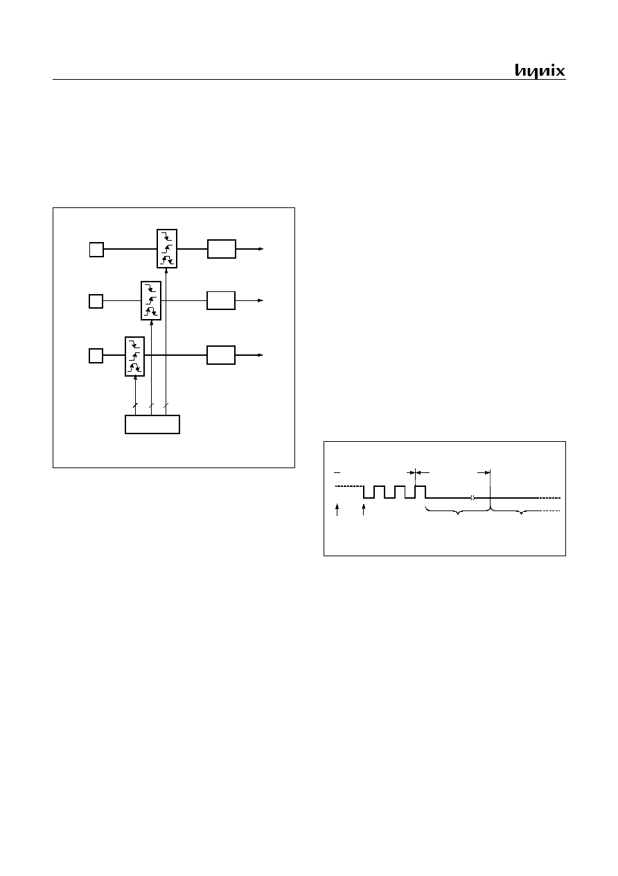
GMS81C7008/7016
68
APR., 2001 Ver 2.01
17.4 External Interrupt
The external interrupt on INT0, INT1 and INT3 pins are edge
triggered depending on the edge selection register IEDS (address
0D8
H
) as shown in Figure 17-7.
The edge detection of external interrupt has three transition acti-
vated mode: rising edge, falling edge, and both edge.
Figure 17-7 External Interrupt Block Diagram
INT0 ~ INT2 are multiplexed with general I/O ports (R00~R02).
To use as an external interrupt pin, the bit of Port Mode Register
PMR should be set to "1" correspondingly as shown in Figure 17-
9.
Example: To use as an INT0 and INT2
:
:
;
**** Set port as an input port R00,R02
LDM
R0DD,#1111_1010B
;
;
**** Set port as an external interrupt port
LDM
PMR,#05H
;
;
**** Set Falling-edge Detection
LDM
IEDS,#0001_0001B
:
:
Response Time
The INT0 ~ INT2 edge are latched into INT1IF ~ INT2IF at every
machine cycle. The values are not actually polled by the circuitry
until the next machine cycle. If a request is active and conditions
are right for it to be acknowledged, a hardware subroutine call to
the requested service routine will be the next instruction to be ex-
ecuted. The DIV itself takes twelve cycles. Thus, a minimum of
twelve complete machine cycles elapse between activation of an
external interrupt request and the beginning of execution of the
first instruction of the service routine.
Figure 17-8 shows interrupt response timings.
Figure 17-8 Interrupt Response Timing Diagram
17.5 Key Scan Interrupt
GMS81C7008/16 has the key-scan block which consists of
Port selection Multiplexer, Interrupt controller, Key scan
mode register and Falling edge detector shown as Figure
17-10.
When the key scan interrupt is used, key scan register
KSMR (address 0F0
H
) should be set to "1" as KS0 and
KS1. After reset, initial setting is general R10 and R00
ports.
If key scan is detected at any one or more of these pins, the
KSIF request flag is set to "1". This generates an interrupt
request. It also can be used in the way of release from
STOP mode.
INT0IF
INT0 pin
INT0 INTERRUPT
INT1IF
INT1 pin
INT1 INTERRUPT
INT2IF
INT2 pin
INT2 INTERRUPT
IEDS
[0D8
H
]
Edge selection
Register
2
2
2
Interrupt
goes
active
Interrupt
latched
Interrupt
processing
Interrupt
routine
8 f
XIN
period
max. 12 f
XIN
period
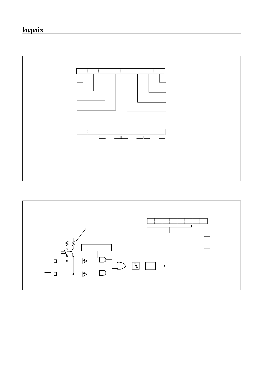
GMS81C7008/7016
APR., 2001 Ver 2.01
69
Figure 17-9 PMR and IEDS Registers
.
Figure 17-10 Key Scan Port Block Diagram
BTCL
BUZ
PWM0
PWM1
INT1S
0: R00
1: INT0
INITIAL VALUE: 00
H
ADDRESS: 0D9
H
PMR
EC2S
INT0S
INT2S
EC0S
0: R01
1: INT1
0: R02
1: INT2
0: R03
1: EC0
0: R32
1: PWM1/T3O
0: R31
1: PWM0/T1O
0: R30
1: BUZ
0: R04
1: EC2
LSB
MSB
BTCL
-
-
R/W
R/W
R/W
R/W
R/W
R/W
IED2H
-
-
IED0H
INITIAL VALUE: 00
H
ADDRESS: 0D8
H
IEDS
IED2L
IED0L
IED1L
IED1H
LSB
MSB
Edge selection register
00: Reserved
01: Falling (1-to-0 transition)
10: Rising (0-to-1 transition)
11: Both (Rising & Falling)
INT0
INT1
INT2
R/W
R/W
R/W
R/W
R/W
R/W
R/W
R/W
Key Scan Interrupt
R10/KS0
R11/KS1
KSIF
V
DD
KSMR
[0F0
H
]
R1PU[1:0]
Key Scan Mode Register
KSMR
ADDRESS: 0F0
H
RESET VALUE: 00
H
-
-
-
-
-
-
KS1 KS0
Port selection
0: R10
1: KS0
Port selection
0: R11
1: KS1
Reserved
Edge detector
Pull up Resistor
Typ. 160k
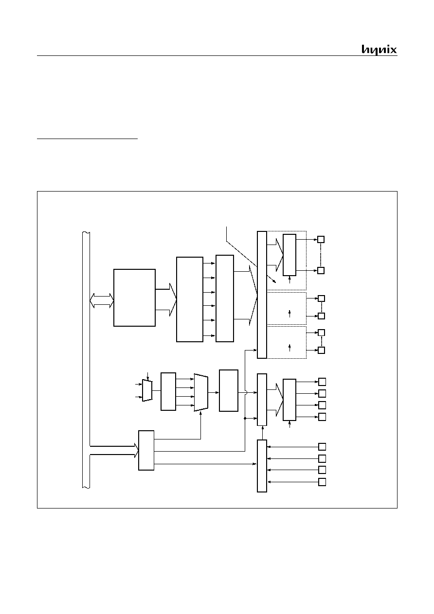
GMS81C7008/7016
70
APR., 2001 Ver 2.01
18. LCD DRIVER
The GMS81C7008/16 has the circuit that directly drives the liq-
uid crystal display (LCD) and its control circuit. In addition,
VCLn pin is provided as the drive power pin.
Basically, the GMS81C7008/16 has 24 seg.
×
4 com. ports of
LCD driver. Extend display modes are shown in left table.
Figure 18-1shows the configuration of the LCD driver.
********Caution********
When you developing the software using by
Emulator, you must select the External bias re-
sistor mode because of no internal bias resistor
inside the Emulator (EVA. chip).
Figure 18-1 LCD Driver Block Diagram
18.1 LCD Control Registers
The LCD driver is controlled by the LCD control register LCR
which is shown in Figure 18-2. LCD block input the clock from
GMS81C7008/16
1/4 duty:
24 seg
×
×
×
×
4com
1/3 duty:
25 seg
×
×
×
×
3com
1/2 duty:
26 seg
×
×
×
×
2com
Static:
27 seg
×
×
×
×
1com
SEG0/R40
Disp
l
a
y
Da
ta
Se
le
ct C
o
n
t
r
o
l
D
i
s
pl
ay
D
a
ta
B
u
ff
er
reg
i
ster
R
4
o
r
S
e
gm
en
t
LC
D
Display Memory
Se
g
m
e
n
t Dr
ive
r
Co
m
m
o
n
Dr
ive
r
(27
×
4 bits)
÷
32
÷
64
÷
128
÷
256
Ti
m
i
ng
C
o
n
t
ro
l
SEG7/R47
LPMR[1:0]
LPMR[3:2]
SEG8/R50
SEG15/R57
LPMR[5:4]
SEG16/R60
SEG23/R67
Select
SEG or Normal port
[0F1
H
]
LCR
INT
E
RNA
L
BUS L
I
NE
Enable LCD
Control bias voltage and resistor
by LPMR [0F2
H
]
MUX
"Same with above"
"Same with above"
WTCK[1:0]
M U X
f
SUB
f
MAIN
÷
2
7
00
01
Pre
scale
r
COM0
COM1/SEG26
COM2/SEG25
COM3/SEG24
LCR[3:2] of address 0F1
H
CO
M
.
o
r
SEG
.
Po
we
r
& Bia
s
c
o
n
t
r
o
l
BIAS
VCL2
VCL1
VCL0
Control frame frequency
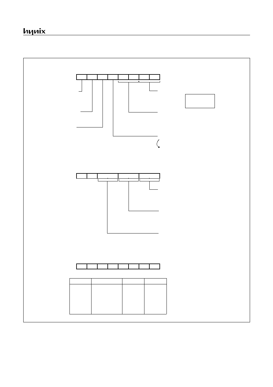
GMS81C7008/7016
APR., 2001 Ver 2.01
71
the Watch Timer. When LCD is operate, the Watch Timer much
be enabled by WTEN (bit 6 of address 0EF
H
).
Figure 18-2 LCD Control Register
7
6
5
4
3
2
1
0
Selection frame frequency
00: 1024Hz
01: 512Hz
10: 256Hz
11: 128Hz
INITIAL VALUE: 00
H
ADDRESS: 0F1
H
LCR
R/W
R/W
R/W
Duty control
00: 1/4 duty
01: 1/3 duty (SEG24 active)
Bias resistor control
0: External
1: Internal
LCD display control
0: LCD display all segment 0 data output
1: LCD display enable
R/W
R/W
R/W
Bias transistor control
0: off
1: on
BTC
SUBM
LCDEN BRC
LCK1 LCK0
R/W
R/W
10: 1/2 duty (SEG24, SEG25 active)
11: Static (SEG24, SEG25, SEG26 active)
Sub clock port mode
0: SXIN, SXOUT
1: R35, R36
DTY0
DTY1
7
6
5
4
3
2
1
0
R4 port selection
00:SEG0~SEG7
01:SEG4~SEG7,R40~R43
10:SEG0~SEG3,R44~R47
11:R40~R47
INITIAL VALUE:0000 0000
ADDRESS: 0F2
H
LPMR
R/W
R/W
R/W
R/W
R5LPMR
R4LPMR
R5 port selection
00:SEG8~SEG15
01:SEG12~SEG15,R50~R53
10:SEG8~SEG11,R54~R57
11:R50~R57
R6LPMR
R6 port selection
00:SEG16~SEG23
01:SEG20~SEG23,R60~R63
10:SEG16~SEG19,R64~R67
11:R60~R67
R/W
R/W
R/W
R/W
-
-
7
6
5
4
3
2
1
0
INITIAL VALUE: 00
H
ADDRESS: 0F3
H
RPR
R/W
R/W
-
RPR1 RPR0
-
-
-
-
-
-
-
-
-
-
-
The RPR register is used for RAM page selection.
RAM page
Instruction
PRP1
PRR0
Page 0
CLRG
X
X
Page 0
SETG
0
0
Page 1
SETG
0
1
Reserved
SETG
1
0
Reserved
SETG
1
1
When
f
SXIN
= 32.768kHz
f
XIN
= 4.19MHz
No internal bias registers in the Emulator,
so user must select the "0", External mode at least
during use the Emulator.
OTP and Mask MCU can use both.
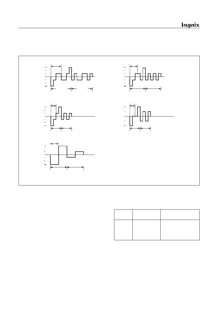
GMS81C7008/7016
72
APR., 2001 Ver 2.01
18.2 Duty and Bias Selection of LCD driver
5 kinds of driving methods can be selected by DTY (bits 3 and 2
of LCD Control Register and connection of VCL pin externally.
Figure 18-3 shows typical driving waveforms for LCD.).
Figure 18-3 LCD drive waveform (Voltage COM-SEG Pins)
18.3 Selecting Frame Frequency
Frame frequency is set to the base frequency as shown in the fol-
lowing Table 18-1.
The LCK[1:0] of LCR determines the frequency of COM signal
scanning of each segment output. The watch timer must be en-
abled when the LCD display is turned on. RESET clears the LCD
control register LCR values to logic zero. The LCD display can
continue to operate even during the SLEEP and STOP modes if a
sub-frequency clock is oscillate and used as clock source of LCD
driver.
.
VCL2
VCL1
VCL0
GND
-VCL0
-VCL1
-VCL2
1/f
F
Data "1"
(a) 1/4 duty, 1/3 bias
Data "0"
VCL2
VCL1
VCL0
GND
-VCL0
-VCL1
-VCL2
1/f
F
Data "1"
(b) 1/3 duty, 1/3 bias
Data "0"
1/f
F
Data "1" Data "0"
(c) 1/2 duty,1/3 bias
1/f
F
Data "1"
Data "0"
VCL2
VCL1
VCL0
GND
-VCL0
-VCL1
-VCL2
(e) Static
Note: f
F
: LCD Frame Frequency
1/f
F
Data "1" Data "0"
VCL2
GND
-VCL0 = -VCL1
-VCL2
(d) 1/2 duty, 1/2 bias
VCL1 = VCL0
VCL2
VCL1
VCL0
GND
-VCL0
-VCL1
-VCL2
LCK[1:0]
LCD clock
Frame Frequency (Hz)
(When f
SUB
= 32.768 kHz)
00
01
10
11
f
SUB
÷
32
f
SUB
÷
64
f
SUB
÷
128
f
SUB
÷
256
1024
512
256
128
Table 18-1 Setting of LCD Frame Frequency
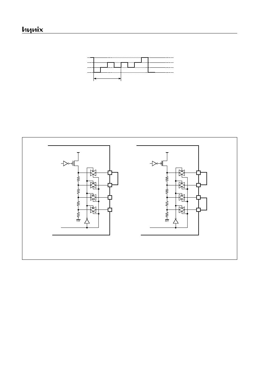
GMS81C7008/7016
APR., 2001 Ver 2.01
73
LCD Port Selection
Segment pins are also used for normal I/O pins. The LCD port se-
lection register LPMR is used to set Rn pin for ordinary digital in-
put. Refer to LPMR register as shown in Figure 18-2.
Bias Resistor
To operate LCD, built-in Bias resistor dividing V
DD
to V
SS
section into several stages generates necessary voltage.
The BTC (Bit 6 of LCR) switches Transistor supplying voltage to
serially connected Bias resistor. If it is `1', it turns on, and if it is
`0', it turns off. The LCD drive voltage (V
CL2
) is given by the dif-
ference in potential (V
DD
-V
CL2
) between pins V
DD
and V
CL2
.
Therefore, when the MCU operating voltage is 5V and LCD drive
voltage are the same, the Bias pin is connected to the V
CL2
pin as
shown in (a) of Figure 18-5.
Figure 18-4 Application Example of 5V LCD Panel
When require supply 3V output to the LCD, the voltage of V
CL2
becomes 3V as shown in Figure 18-5. Because V
DD
is down to
3V through internal 2R resistor.
The LCD light only when the difference in potential between the
segment and common output is ±VCL, and turn off at all other
times. During reset, the power switch of the LCD driver is turned
off automatically, shutting off the VCL voltage.
one frame
(at 1/4 duty, 1/3 bias)
COM0 pin
VCL1
VCL2
BIAS
BTC
V
DD
V
SS
(a) Internal, Static or 1/3 Bias
BTC = "1"
BRC = "1"
In
ter
nal
B
i
a
s
re
sisto
r
s
MCU Internal
VCL0
BRC
2R
R
R
R
BTC
V
DD
V
SS
(b) Internal, Static or 1/2 Bias
BTC = "1"
BRC = "1"
Two pins are connected
each other
In
ter
nal
B
i
a
s
re
sisto
r
s
MCU Internal
BRC
2R
R
R
R
Typ. R=65k
VCL1
VCL2
BIAS
VCL0
Short two pins
each other externally
VCL2=5V
VCL1=3.33V
VCL0=1.67V
VCL2=5V
VCL1=2.5V
VCL0=2.5V
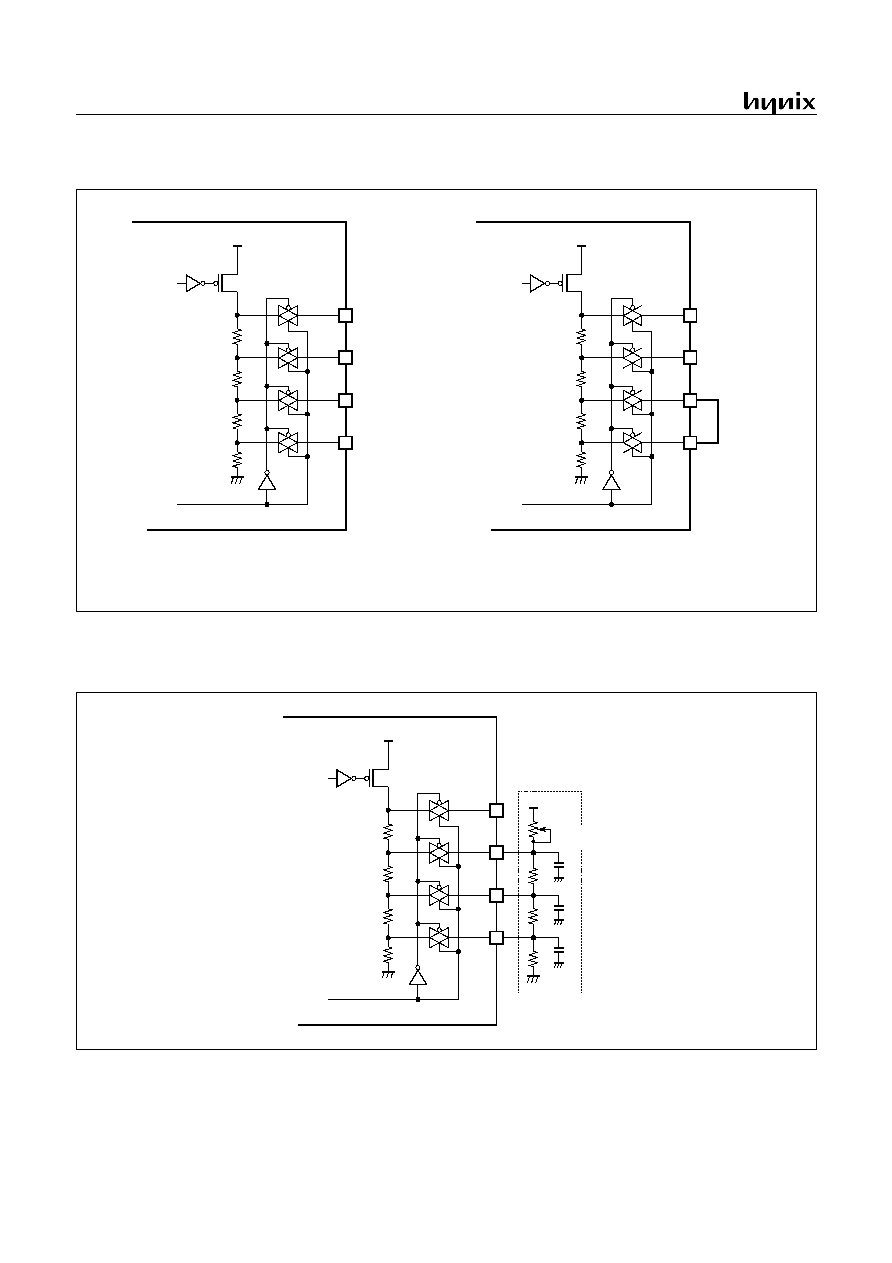
GMS81C7008/7016
74
APR., 2001 Ver 2.01
Figure 18-5 Application Example of 3V LCD Panel
Some user want to use external bias resisor instead of internal,
you can connect external resistor as shown in Figure 18-6. And
the external capacitors are may required for stable display accord-
ing to your system environment.
Figure 18-6 External Resistor
VCL1
VCL2
BIAS
BTC
V
DD
= 5V
V
SS
(a) Internal, Static or 1/3 Bias
BTC = "1"
BRC = "1"
Short two pins
externally
In
ter
nal B
i
a
s
re
sistor
s
MCU Internal
VCL0
BRC
2R
R
R
R
Typ. R=65k
BTC
V
DD
= 5V
V
SS
(b) Internal, Static or 1/2 Bias
BTC = "1"
BRC = "1"
In
ter
nal B
i
a
s
re
sistor
s
MCU Internal
BRC
2R
R
R
R
Typ. R=65k
VCL1
VCL2
BIAS
VCL0
VCL2=3V
VCL1=2V
VCL0=1V
VCL2=3V
VCL1=1.5V
VCL0=1.5V
VCL1
VCL2
BIAS
BTC
V
DD
V
SS
BTC = "0"
BRC = "0"
External circuit
In
ter
nal
B
i
a
s
re
sisto
r
s
MCU Internal
VCL0
BRC
2R
R
R
R
V
SS
V
DD
Adjust Contrast
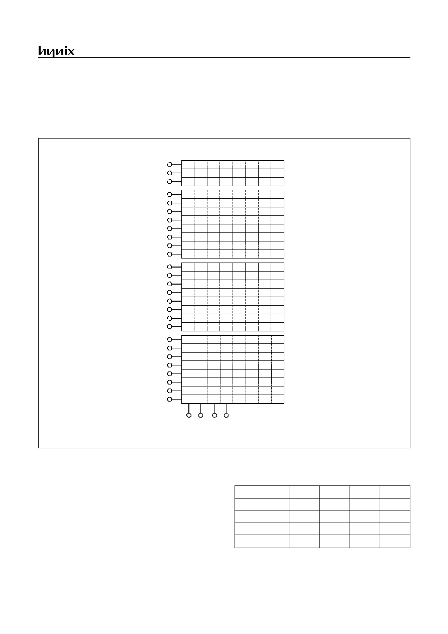
GMS81C7008/7016
APR., 2001 Ver 2.01
75
18.4 LCD Display Memory
Display data are stored to the display data area (address
100
H
-11A
H
) in the data memory.
The display data stored to the display data area are read au-
tomatically and sent to the LCD driver by the hardware.
The LCD driver generates the segment signals and com-
mon signals in accordance with the display data and drive
method.
Figure 18-7
LCD Display Memory
Therefore, display patterns can be changed by only over-
writing the contents of the display data area with a pro-
gram. The table look up instruction is mainly used for this
overwriting.
Figure 18-7 shows the correspondence between the display
data area and the SEG/COM pins. The LCD lights when
the display data is "1" and turn off when "0".
The number of segment which can be driven differs de-
pending on the LCD drive method, therefore, the number
of display data area bits used to store the data also differs
(Refer to Figure 18-2). Consequently, data memory not
SEG0
SEG1
SEG2
SEG3
SEG4
SEG5
SEG6
SEG7
COM
0
COM
1
COM
2
COM
3
SEG8
SEG9
SEG10
SEG11
SEG12
SEG13
SEG14
SEG15
SEG16
SEG17
SEG18
SEG19
SEG20
SEG21
SEG22
SEG23
SEG24
SEG25
SEG26
0
1
2
3
4
5
6
7
Bit
100
H
101
H
102
H
103
H
104
H
105
H
106
H
107
H
108
H
109
H
10A
H
10B
H
10C
H
10D
H
10E
H
10F
H
110
H
111
H
112
H
113
H
114
H
115
H
116
H
117
H
118
H
119
H
11A
H
Note:
The bit 4 to 7 of every byte are
reserved. Any read or write is not
effect.
Drive methods
Bit 3
Bit 2
Bit 1
Bit 0
1/4 duty
COM3
COM2
COM1
COM0
1/3 duty
-
COM2
COM1
COM0
1/2 duty
-
-
COM1
COM0
Static
-
-
-
COM0
Table 18-2 The duty vs. COM port Configuration
GMS81C7008/7016
76
APR., 2001 Ver 2.01
used to store display data and data memory for which the
address are not connected to LCD can be used to store or-
dinary user's processing data.
Blanking
Blanking is applied by setting LCDEN (bit 7 of LCR) to "0" and
turns off the LCD by outputting the non light operation level to
the COM pin. When setting Frame frequency or changing operat-
ing mode, LCD display should be off before operation, to prevent
display flickering.
18.5 Control Method of LCD Driver
Initial Setting
Flow chart of initial setting is shown in Figure 18-8.
Example: When operating with 1/4 duty LCD using a
frame frequency of 512Hz.
.
Figure 18-8 Initial Setting of LCD Driver
Figure 18-9 Example of Connection COM & SEG
Display Data Setting
Normally, display data are kept permanently in the pro-
gram memory and then stored at the display data area by
the table look-up instruction. This can be explained using
numerical display with 1/4 duty LCD as an example. The
COM and SEG connections to the LCD and display data
are the same as those shown is Figure 18-9. Programming
LDM
LCR,#0101_0001B ;1/4duty, f
F
=512Hz
(f
SUB
= 32.768kHz)
:
SETG
LDM
RPR,#1
;Select LCD Memory
;area (Page 1 = address 1XX
H
)
LDX
#0
C_LCD1:
LDA
#0
;RAM Clear
;RAM(100H~11AH)
STA
{X}+
CMPX
#01BH
BNE
C_LCD1
CLRG
:
:
SET1
LCR.5
;Enable LCD display
:
:
Clear
LCD Display
Memory
Select Frame Frequency
Turn on LCD
Setting of LCD drive method
Initialize of display memory
Enable display
(Release of blanking)
SEG0
SEG1
COM3
COM0
COM1
COM2
Example: display "2"
1
1
1
0
0
1
0
1
*
*
*
*
*
*
*
*
100
H
101
H
3
1
2
0
bit 7
5
6
4
Note: * are don't care.

GMS81C7008/7016
APR., 2001 Ver 2.01
77
example for displaying character is shown below.
Note: When power on RESET, sub oscillation start up time
is required. Enable LCD display after sub oscillation is sta-
bilized, or LCD may occur flicker at power on time shortly.
:
CLRG
LDX
#DISPRAM
GOLCD:
LDA
{X}
TAY
LDA
!FONT+Y
;LOAD FONT DATA
LDM
RPR,#1
;Set RPR = 1 to access LCD
SETG
;Set Page 1
LDX
#0
STA
{X}+
;LOWER 4 BITS OF ACC. -> M(X)
XCN
STA
{X}
;UPPER 4 BITS OF ACC. -> M(X+1)
CLRG
;Set Page = 0
:
:
FONT
DB
1101_0111B
; "0"
DB
0000_0110B
; "1"
DB
1110_0011B
; "2"
DB
1010_0111B
; "3"
DB
0011_0110B
; "4"
DB
1011_0101B
; "5"
DB
1111_0101B
; "6"
DB
0000_0111B
; "7"
DB
1111_0111B
; "8"
DB
0011_0111B
; "9"
Font data
Write into the
LCD Memory
GMS81C7008/7016
78
APR., 2001 Ver 2.01
19. WATCH / WATCHDOG TIMER
19.1 Watch Timer
The watch timer goes the clock continuously even during the
power saving mode. When MCU is in the Stop or Sleep mode,
MCU can wake up itself every 2Hz or 4Hz or 16Hz.
The watch timer consists of input clock selector, 14-bit binary
counter, interval selector and Watch Timer Mode Register
WTMR (address 0EF
H
). The WTMR is 5-bit read/write register
and shown in Figure 19-2. WTMR can select the clock input by
2 bits WTCK[1:0] and interval time selector by 2 bits WTIN[1:0]
and enable/disable bit. The WTEN bit is set to "1" timer start
counting. Input clocks can be selected among three different
source which are sub clock or divided main clock (f
XIN
÷
128) or
main clock. For the switching between main and sub clock, rec-
ommend the oscillator 4.194304MHz as a main and 32.768kHz
as a sub. Because above main frequency is equal to 128 times of
sub frequency. Generally main clock (f
XIN
) at WTCK=10
B
is not
be used, it is just for test purpose in factory.
In the Stop Mode, the main clock is stopped but sub clock is os-
cillation continuously for watch clock operation. Output timer in-
terval can be selected and Watch Timer Interrupt is generated.
LDM
IENL,#XXXX_X1XXB
EI
LDM
WTMR,#0100_1000B
Figure 19-1 Block Diagram of Watchdog Timer
19.2 Watchdog Timer
The watchdog timer rapidly detects the CPU malfunction such as
endless looping caused by noise or the like, and resumes the CPU
to the normal state.
The watchdog timer signal for detecting malfunction can be se-
lected either a reset CPU or a interrupt request as you want.
When the watchdog timer is not being used for malfunction de-
tection, it can be used as a timer to generate an interrupt at fixed
intervals.
Watchdog Timer Control
Figure 19-2 shows the watchdog timer control register WDTR
(address 0DF
H
). The watchdog timer is automatically enabled
initially and watchdog output to reset CPU but clock input source
is disabled. To enable this function, you should write bit WTEN
of WTMR (address 0EF
H
) set to "1".
The CPU malfunction is detected during setting of the detection
time, selecting of output, and clearing of the binary counter.
Clearing the 2-bit binary counter by bit WDCLR of WDTR is re-
peated within the detection time.
If the malfunction occurs for any cause, the watchdog timer out-
put will become active from the binary counters unless the binary
counter is cleared. At this time, when WDOM=1, a reset is gen-
erated, which drives the RESET pin to low to reset the internal
hardware. When WDOM=0, a watchdog timer interrupt (WD-
TIF) is generated instead of Reset function. This interrupt can be
used general timer as user want.
When main clock is selected as clock input source on the STOP
mode, clock input is stopped so the watchdog timer temporarily
stops counting. The other side, when sub clock is selected as
clock input source on the STOP mode, sub clock operates always
enable
Watch Timer interrupt
WTIF
0
1
14-bit Binary Counter
MUX
f
SXIN
f
XIN
÷
128
f
XIN
f
W
f
SXIN
= 32.768 kHz
f
XIN
= 4.194304 MHz
Interval Selector
2H
z
4H
z
16
H
z
2H
z
4H
z
8H
z
16
H
z
2-bit Binary Counter
WDCK[1:0]
WTIN[1:0]
WTCK[1:0]
WDOE[0DF
H
]
R34/WDTO
clea
r
0: Stop
1: Clear and start
WDCLR
WDTIF
to RESET CPU
Watchdog Timer Interrupt
overflow
WDEN
WDOM
00
01
10
00
01
10 11
00
01
10
enable
0
1
WTEN
MUX
When
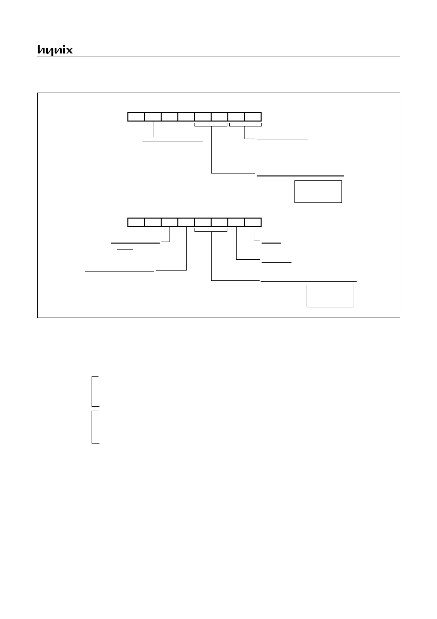
GMS81C7008/7016
APR., 2001 Ver 2.01
79
so the watchdog timer works continuously.
Figure 19-2 WTMR, WDTR: Watch Timer and Watchdog Timer Data Register
Example: Sets the watchdog timer detection time to 1 sec at 4.19MHz, 32.768kHz
Enable and Disable Watchdog
Watchdog timer is enabled by setting WDEN (bit 4 in CKCTLR)
to "1". WDEN is initialized to "1" during reset and it should be
clear to "0" disable.
Example: Enables watchdog timer for Reset
:
LDM
WTMR,#0100_XXXXB;
WTEN
1
LDM
WDTR,#00X1_XX11B;
WDEN
1
:
The watchdog timer is disabled by clearing either bit 4 (WDEN)
of WDTR or bit 6 (WTEN) of WTMR. The watchdog timer is
halted in STOP mode and restarts automatically after STOP mode
is released.
Clearing 2-bit binary counter of the Watchdog
timer
The watchdog timer count the clock source as 14-bit binary
INITIAL VALUE: -0--_0000
B
ADDRESS: 0EF
H
WTMR
-
-
WTEN
WTIN1 WTIN0
-
R/W
R/W
R/W
-
R/W
R/W
-
-
WTCK1 WTCK0
Clock source selection
00: Sub clock
01: Main clock (f
XIN
÷
128)
10: Main clock (test purpose in factory)
11: -
Watch timer interrupt interval selection
00: 16Hz
01: 4Hz
10: 2Hz
11: -
Watch Timer count enable
0: Disable
1: Enable
INITIAL VALUE: --01_0010
B
ADDRESS: 0DF
H
WDTR
-
W D O E
W D C K 1 W D C K 0
R/W
R/W
R/W
-
-
R/W
-
W D E N
W D O M W D C LR
Watchdog timer interrupt interval selection
00: 2 sec.
01: 1 sec.
10: 0.5 sec.
11: 0.25 sec.
R34/WDTO selection
0: R34 port
1: WDTO port
R/W
R/W
Clear bit
0: Normal operation
1: Clear and starts counting
When
f
SXIN
= 32.768kHz
f
XIN
= 4.19MHz
Output Mode
0: Interrupt request
1: Reset CPU
Watchdog Timer count enable
0: Disable
1: Enable
When
f
SXIN
= 32.768kHz
f
XIN
= 4.19MHz
LDM
WTMR,#0100_1000B
;
Select sub clock as an input source
LDM
WDTR,#0001_0111B
SET1
WDCLR
;
Clear counter
:
:
:
:
SET1
WDCLR
;
Clear counter
:
:
:
:
SET1
WDCLR
;
Clear counter
Within 0.75 sec.
Within 0.75 sec.
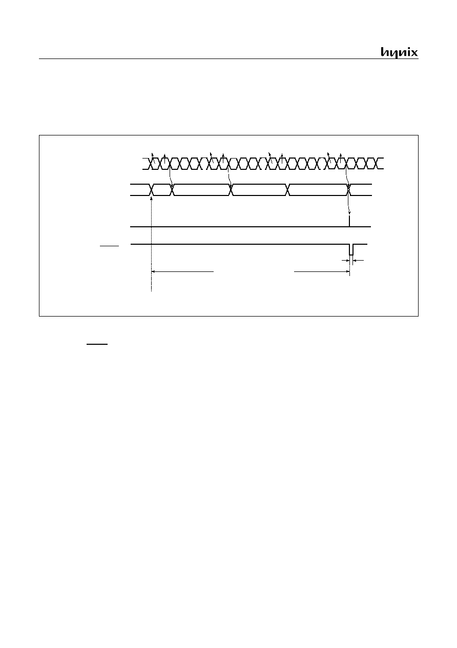
GMS81C7008/7016
80
APR., 2001 Ver 2.01
counter which is free run can not be cleared. The watchdog timer
has 2-bit binary counter. It is incremented by 14-bit binary
counter match as shown in Figure 19-1. Interrupt request flag or
Reset signal are generated by overflow 2-bit binary counter.
During normal operation in the software, 2-bit binary counter
should be cleared by bit WDCLR of WDTR within watchdog
timer overflow.
The time of clearing must be within 3 times of 14-bit binary
counter interval as shown in Figure 19-3.
The worst case, watchdog time is just 3 times of 14-bit counter.
Figure 19-3 Watchdog timer Timing
If the watchdog timer output becomes active, a reset is generated,
which drives the RESET pin low to reset the internal hardware.
The main clock oscillator also turns on when a watchdog timer re-
set is generated in sub clock mode.
14-bit binary
2-bit binary
WDTIF interrupt
Write WDCLR = 1 at this point
1
0
Counter
Clear
n
counter
R34/WDTO pin
reset
0
1
1FFE
~~
~~
1FFF
counter
0
2
3
0
1
1FFE
1FFF
0
1
1FFE
1FFF
~~
~~
0
1
1FFE
1FFF
2
2
2
2
~~
~~
8 osc.
(2us at f
XIN
=4.19MHz)
Even if user set to 1 sec.,
When WDTR = 0011_0111B
worst case 0.75 second
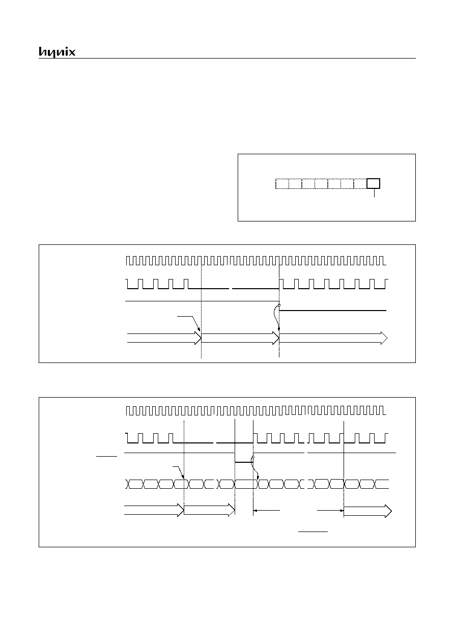
GMS81C7008/7016
APR., 2001 Ver 2.01
81
20. POWER DOWN OPERATION
The GMS81C7008/16 has two power-down modes. In power-
down mode, power consumption is reduced considerably that in
Battery operation Battery life can be extended a lot.
Sleep mode is entered by setting bit 0 of Sleep Mode Reg-
ister, and STOP Mode is entered by STOP instruction.
20.1 SLEEP Mode
In this mode, the internal oscillation circuits remain active.
Oscillation continues and peripherals are operate normally but
CPU stops. Movement of all Peripherals is shown in Table 20-1.
Sleep mode is entered by setting bit 0 of SMR (address 0DE
H
).
It is released by RESET or interrupt. To be release by interrupt,
interrupt should be enabled before Sleep mode.
Figure 20-1 SLEEP Mode Register
Figure 20-2 Sleep Mode Release Timing by External Interrupt
.
Figure 20-3 SLEEP Mode Release Timing by RESET pin
Sleep Mode Register
SMR
ADDRESS : 0DE
H
RESET VALUE : -------0
0: Release Sleep Mode
1: Enter Sleep Mode
W
Oscillator
Normal Operation
Stand-by Mode
Normal Operation
Interrupt
Internal CPU Clock
Release
Set bit 0 of SMR
(X
IN
or SX
IN
pin)
~~
~~
Oscillator
(X
IN
or SX
IN
pin)
0
BIT Counter
1
FE
FF
0
1
2
~~
t
ST
= 62.5ms
~~
~~
RESET
Internal CPU Clock
Clear & Start
~~
~~
Normal Operation
Sleep Mode
Normal Operation
Release
Set bit 0 of SMR
~~
~~
~~
at 4.19MHz by hardware
~~
2
t
ST
=
x 256
f
MAIN
÷
1024
1
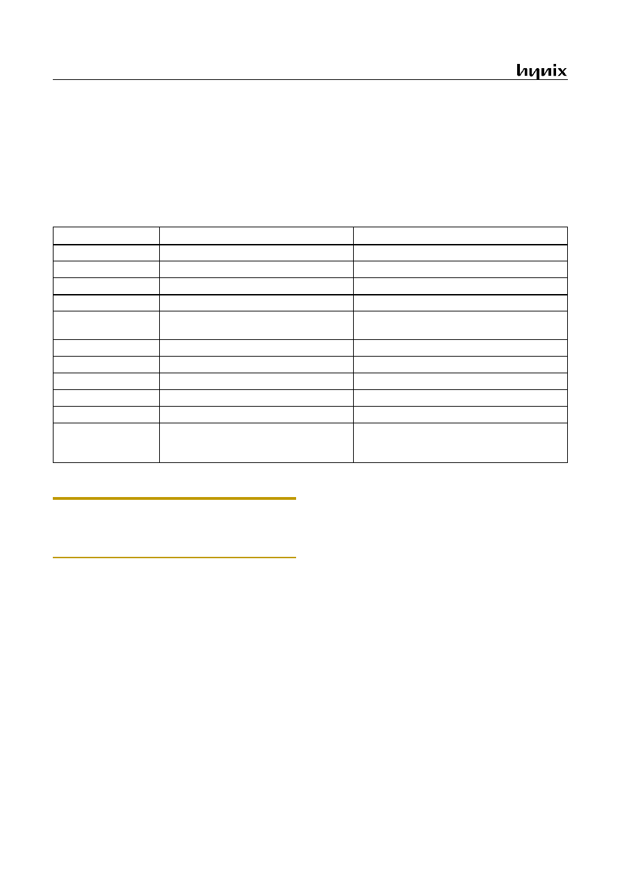
GMS81C7008/7016
82
APR., 2001 Ver 2.01
20.2 STOP Mode
For applications where power consumption is a critical
factor, device provides reduced power of STOP.
Start The Stop Operation
An instruction that STOP causes to be the last instruction
is executed before going into the STOP mode. In the Stop
mode, the on-chip main-frequency oscillator is stopped.
With the clock frozen, all functions are stopped, but the on-
chip RAM and Control registers are held. The port pins
output the values held by their respective port data register,
the port direction registers. The status of peripherals during
Stop mode is shown below.
Note: Since the X
IN
pin is connected internally to GND to
avoid current leakage due to the crystal oscillator in STOP
mode, do not use STOP instruction when an external clock
is used as the main system clock.
In the Stop mode of operation, V
DD
can be reduced to minimize
power consumption. Be careful, however, that V
DD
is not re-
duced before the Stop mode is invoked, and that V
DD
is restored
to its normal operating level before the Stop mode is terminated.
The reset should not be activated before V
DD
is restored to its
normal operating level, and must be held active long enough to
allow the oscillator to restart and stabilize.
And after STOP instruction, at least two or more NOP instruction
should be written as shown in example below.
Example)
LDM
CKCTLR,#0EB ;32.8ms
;
LDM
CKCTLR,#0FB ;65.5ms
STOP
NOP
NOP
:
The Interval Timer Register CKCTLR should be initialized (0F
H
or 0E
H
) by software in order that oscillation stabilization time
should be longer than 20ms before STOP mode.
Release the STOP mode
The exit from STOP mode is using hardware reset or external in-
terrupt, watch timer, key scan or timer/counter.
To release STOP mode, corresponding interrupt should be
enabled before STOP mode.
Specially as a clock source of Timer/Event counter, EC0 or EC2
pin can release it by Timer/Event counter
Interrupt request
Reset redefines all the control registers but does not change the
on-chip RAM. External interrupts allow both on-chip RAM and
Control registers to retain their values.
Start-up is performed to acquire the time for stabilizing oscilla-
tion. During the start-up, the internal operations are all stopped.
Peripheral
STOP Mode
SLEEP Mode
CPU
All CPU operations are disabled
All CPU operations are disabled
RAM
Retain
Retain
LCD driver
LCD driver operates continuously
LCD driver operates continuously
Basic Interval Timer
Halted
BIT operates continuously
Timer/Event counter
Halted (Only when the Event counter mode
is enabled, Timer operates normally)
Timer/Event counter operates continuously
Watch Timer
Watch Timer operates continuously
Watch Timer operates continuously
Main-oscillation
Stop (X
IN
pin = "L", X
OUT
pin = "L")
Oscillation
Sub-oscillation
Oscillation
Oscillation
I/O ports
Retain
Retain
Control Registers
Retain
Retain
Release method
RESET, Key Scan interrupt, SIO interrupt,
Watch Timer interrupt, Timer interrupt
(EC0,2), External interrupt
RESET, All interrupts
Table 20-1 Peripheral Operation during Power Down Mode
GMS81C7008/7016
APR., 2001 Ver 2.01
83
Figure 20-4 STOP Mode Release Timing by External Interrupt
Figure 20-5 STOP Mode Release Timing by RESET
Minimizing Current Consumption
The Stop mode is designed to reduce power consumption.
To minimize current drawn during Stop mode, the user
should turn-off output drivers that are sourcing or sinking
current, if it is practical.
Note: In the STOP operation, the power dissipation asso-
ciated with the oscillator and the internal hardware is low-
ered; however, the power dissipation associated with the
pin interface (depending on the external circuitry and pro-
gram) is not directly determined by the hardware operation
of the STOP feature. This point should be little current flows
when the input level is stable at the power voltage level
(V
DD
/V
SS
); however, when the input level becomes higher
than the power voltage level (by approximately 0.3V), a cur-
rent begins to flow. Therefore, if cutting off the output tran-
sistor at an I/O port puts the pin signal into the high-
impedance state, a current flow across the ports input tran-
sistor, requiring it to fix the level by pull-up or other means.
Before executing Stop instruction, Basic Interval Timer must be set
Oscillator
(X
IN
pin)
~~
n
0
BIT Counter
n+1
n+2
n+3
~~
Normal Operation
Stop Operation
Normal Operation
1
FE
FF
0
1
2
~~
~~
~~
t
ST
>
20ms
~~
~~
External Interrupt
Internal Clock
Clear
STOP Instruction
Executed
~~
~~
~~
properly by software to get stabilization time which is longer than 20ms.
by software
~~
Oscillator
(X
IN
pin)
~~
n
0
BIT Counter
n+1
n+2
n+3
~~
Normal Operation
Stop Operation
Normal Operation
1
FE
FF
0
1
2
~~
~~
~~
t
ST
> 62.5ms
Internal Clock
Clear
STOP Instruction
Executed
~~
~~
~~
at 4.19MHz by hardware
~~
RESET
n+2
t
ST
=
x 256
f
MAIN
÷
1024
1
~~
~~
GMS81C7008/7016
84
APR., 2001 Ver 2.01
It should be set properly that current flow through port doesn't ex-
ist.
First consider the setting to input mode. Be sure that there is no
current flow after considering its relationship with external cir-
cuit. In input mode, the pin impedance viewing from external
MCU is very high that the current doesn't flow.
But input voltage level should be V
SS
or V
DD
. Be careful that if
unspecified voltage, i.e. if un-firmed voltage level (not V
SS
or
V
DD
) is applied to input pin, there can be little current (max. 1mA
at around 2V) flow.
If it is not appropriate to set as an input mode, then set to output
mode considering there is no current flow. Setting to High or Low
is decided considering its relationship with external circuit. For
example, if there is external pull-up resistor then it is set to output
mode, i.e. to High, and if there is external pull-down register, it is
set to low.
Figure 20-6 Application Example of Unused Input Port
Figure 20-7 Application Example of Unused Output Port
INPUT PIN
V
DD
GND
i
V
DD
X
Weak pull-up current flows
V
DD
internal
pull-up
INPUT PIN
i
V
DD
X
Very weak current flows
V
DD
O
O
OPEN
OPEN
i=0
O
i=0
O
GND
When port is configure as an input, input level should
be closed to 0V or 5V to avoid power consumption.
OUTPUT PIN
GND
i
In the left case, much current flows from port to GND.
X
ON
OFF
OUTPUT PIN
GND
i
In the left case, Tr. base current flows from port to GND.
i=0
X
OFF
ON
V
DD
L
ON
OFF
OPEN
GND
V
DD
L
ON
OFF
To avoid power consumption, there should be low output
ON
OFF
O
O
V
DD
O
to the port .
GMS81C7008/7016
APR., 2001 Ver 2.01
85
21. OSCILLATOR CIRCUIT
The GMS81C7008/16 has two oscillation circuits internally. X
IN
and X
OUT
are input and output for main frequency and SX
IN
and
SX
OUT
are input and output for sub frequency, respectively, in-
verting amplifier which can be configured for being used as an
on-chip oscillator, as shown in Figure 21-1. To use RC oscillation
instead of crystal, user should check mark on the "A. MASK OR-
DER SHEET" on page i of the appendix of this manual. However
in the OTP device, when the programming RC oscillation can be
selected or not into the configuration bit. For more detail, refer to
"24.1 OTP Programming" on page 89.
Note: When using the sub clock oscillation, connect a re-
sistor in series with R which is shown as below figure.
In order to reduce the power consumption, the sub clock
oscillator employs a low amplification factor circuit. Be-
cause of this, the sub clock oscillator is more sensitive to
noise than the main system clock oscillator.
Figure 21-1 Oscillation Circuit
Oscillation circuit is designed to be used either with a ceramic
resonator or crystal oscillator. Since each crystal and ceramic res-
onator have their own characteristics, the user should consult the
crystal manufacturer for appropriate values of external compo-
nents.
Oscillation circuit is designed to be used either with a ceramic
resonator or crystal oscillator. Since each crystal and ceramic res-
onator have their own characteristics, the user should consult the
crystal manufacturer for appropriate values of external compo-
nents. In addition, see Figure 21-2 for the layout of the crystal.
Note: Minimize the wiring length. Do not allow the wiring to
intersect with other signal conductors. Do not allow the wir-
ing to come near changing high current. Set the potential of
the grounding position of the oscillator capacitor to that of
V
SS
. Do not ground it to any ground pattern where high cur-
rent is present. Do not fetch signals from the oscillator.
Figure 21-2 Recommend Layout of Oscillator PCB
circuit
X
OUT
X
IN
V
SS
Recommend
C1,C2 = 20pF
C1
C2
X
OUT
X
IN
External Clock
Open
X
OUT
X
IN
External Oscillator
RC Oscillator (mask option)
Crystal or Ceramic Oscillator
SX
OUT
SX
IN
V
SS
Recommend
C1,C2 = 30pF±5pF
C1
C2
32.768kHz
4.19MHz
Crystal Oscillator
Ceramic Resonator
C1,C2 = 30pF
Refer to AC Characteristics
For selection R value,
R
EXT
R
R= 47k
±5k
X
OUT
X
IN
GMS81C7008/7016
86
APR., 2001 Ver 2.01
22. RESET
The GMS81C7008/16 has two types of reset generation proce-
dures; one is an external reset input, the other is a watch-dog tim-
er reset. Table 22-1 shows on-chip hardware initialization by
reset action.
Figure 22-1 Simple Power-on-Reset Circuit.
22.1 External Reset Input
The reset input is the RESET pin, which is the input to a Schmitt
Trigger. A reset in accomplished by holding the RESET pin low
for at least 8 oscillator periods, within the operating voltage range
and oscillation stable, it is applied, and the internal state is initial-
ized. After reset, 64ms (at 4 MHz) add with 7 oscillator periods
are required to start execution as shown in Figure 22-2.
Internal RAM is not affected by reset. When V
DD
is turned on,
the RAM content is indeterminate. Therefore, this RAM should
be initialized before read or tested it.
When the RESET pin input goes to high, the reset operation is re-
leased and the program execution starts at the vector address
stored at addresses FFFE
H
- FFFF
H
.
A connection for simple power-on-reset is shown in Figure .
Figure 22-2 Timing Diagram after RESET
22.2 Watchdog Timer Reset
Refer to "18. LCD DRIVER" on page 70.
7036P
V
CC
10uF
+
10k
to the RESET pin
On-chip Hardware
Initial Value
Program counter (PC)
(FFFF
H
) - (FFFE
H
)
G-flag (G)
0
Operation mode
Main operating mode
Peripheral clock
On
Watchdog timer
Disable (Because the Watch
timer is disabled)
Control registers
Refer to Table 8-1 on
page 25
Low voltage detector
Enable
Table 22-1 Initializing Internal Status by Reset Action
MAIN PROGRAM
Oscillator
(X
IN
pin)
?
?
FFFE FFFF
Stabilization Time
t
ST
= 62.5mS at 4.19MHz
RESET
ADDRESS
DATA
1
2
3
4
5
6
7
?
?
Start
?
?
?
FE
?
ADL
ADH
OP
BUS
BUS
RESET Process Step
~~
~~
~~
~~
~~
~~
t
ST
=
x 256
f
MAIN
÷
1024
1
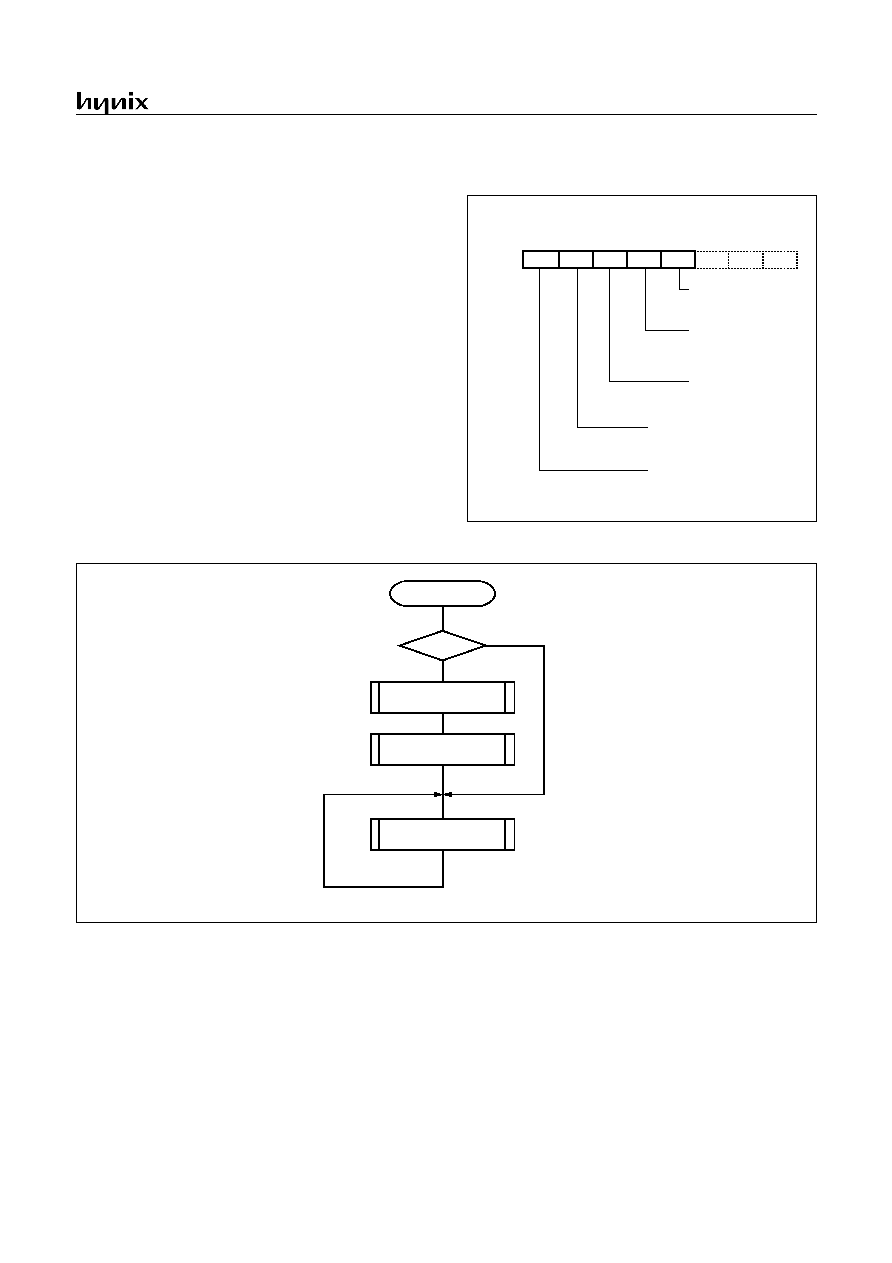
GMS81C7008/7016
APR., 2001 Ver 2.01
87
23. POWER FAIL PROCESSOR
The GMS81C7008/16 has an on-chip low voltage detection cir-
cuitry to detect the V
DD
voltage. A configuration register, LVDR
(address 0FB
H
), can enable or disable the low voltage detect cir-
cuitry. Whenever V
DD
falls close to or below 2.2V, the LVD0 is
just set to "1", and if it recovering 3.4V, LVD0 is held to "1". If
V
DD
falls below around 3.4V range, the low voltage situation
may reset the MCU or freeze the clock according to setting of bit
5 (LVDM) of LVDR . The bit 4 LVD1 function is same with
LVD0 except different voltage level 2.1V. The detection voltage
is varied very little. See "7.3 DC Electrical Characteristics" on
page 11 for more detail voltage level.
In the in-circuit emulator, power fail function is not implemented
and user may not use it. Therefore, after completed development
of user program, this function may be experimented or evaluated
using by OTP.
When power fail certainly occur the MCU was reset, program no-
tify this Reset circumstance cause by LVD function. So, does not
erase the all RAM contents and operates subsequently as shown
in Figure .
Figure 23-1 Low Voltage Detector Register
7
6
5
4
3
2
1
0
LVDE
INITIAL VALUE: 00
H
ADDRESS: 0FB
H
LVDR
R/W
R/W
R/W
LVD1
Operation Mode
0: Clock freeze
1: Reset
Enable / Disable Flag
0: Disable
1: Enable
LVDS
LVD0
Power Fail Voltage Selection
0: 3.4V
1: 2.1V
R/W
LVDM
V
DD
Detection Flag 1
0: Above 3.4V
1: Below 3.4V
V
DD
Detection Flag 2
0: Above 2.1V
1: Below 2.1V
Figure 23-2 Example S/W of RESET by Power fail
FUNTION
EXECUTION
INITIALIZE RAM DATA
LVD0 =1
NO
RESET VECTOR
INITIALIZE ALL PORTS
INITIALIZE REGISTERS
RAM CLEAR
YES
Skip the initial routine when
the Reset cause from power fail.
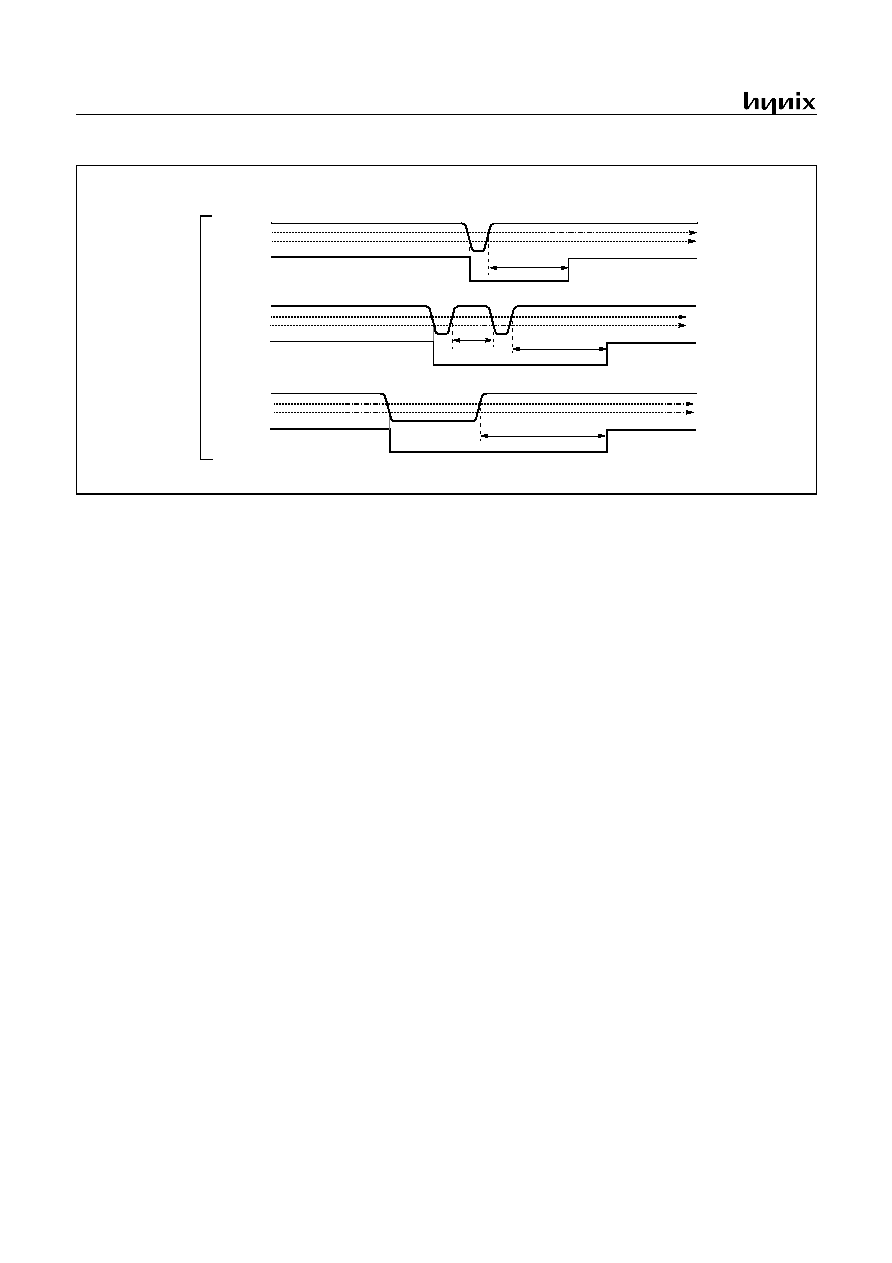
GMS81C7008/7016
88
APR., 2001 Ver 2.01
Figure 23-3 Power Fail Processor Situations
Internal
RESET
Internal
RESET
Internal
RESET
V
DD
V
DD
V
DD
LVDV
DD
MAX
LVDV
DD
MIN
LVDV
DD
MAX
LVDV
DD
MIN
LVDV
DD
MAX
LVDV
DD
MIN
64mS
64mS
t <64mS
64mS
When LVDM = 1
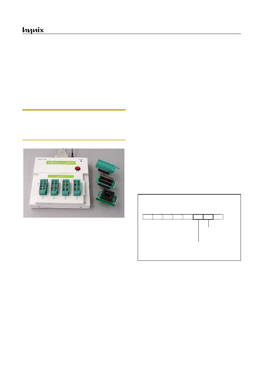
GMS81C7008/7016
APR., 2001 Ver 2.01
89
24. DEVELOPMENT TOOLS
24.1 OTP Programming
The GMS87C7016 is OTP (One Time Programmable) type mi-
crocontrollers. Its internal user memory is constructed with
EPROM (Electrically Programmable Read Only Memory).
The OTP microcontroller is generally used for chip evaluation,
first production, small amount production, fast mass production,
etc.
Blank OTP's internal EPROM is filled by 00
H
, not FF
H
.
Note: In any case, you have to use the *.OTP file for pro-
gramming, not the *.HEX file. After assemble the source
program, both OTP and HEX file are generated by automat-
ically. The HEX file is used during program emulation on
the emulator.
How to Program
To program the OTP devices, user should use HEI own program-
mer. Ask to HEI sales part for purchasing or more detail.
Programmer: CHOICE-SIGMA (Single type)
CHOICE-GNAG4 (4-gang type)
Socket adapter:87C70XX-64SD (for 64SDIP)
87C70XX-64QF (for 64MQFP)
The CHOICE-SIGMA is a HEI Universal Single Programmer for
all of HEI OTP devices, also the CHOICE-GANG4 can program
four OTPs at once.
Programming Procedure
1. Select device GMS87C7016 as you want.
2. Load the *.OTP file from the PC to Programmer. The
file is composed of Motorola-S1 format.
3. Set the programming address range as below table.
4. Mount the socket adapter on the programmer.
5. Set the configuration bytes as your needs.
6. Start program/verify.
Select the option for Program Lock and RC oscil-
lation
Except the user program memory C000
H
~FFFF
H
, there is config-
uration byte (address 707F
H
) for the selection of program lock
and RC oscillation. The configuration byte of OTP is shown as
Figure 24-1. It could be served when user use the OTP program-
mer (Choice-Sigma or Choice-Gang4).
Figure 24-1 The OTP Configuration Byte
87C70XX-64SD
87C70XX-64QF
87C71XX-52SD
ADDRESS: 707F
H
7
6
5
4
3
2
1
0
OTP Configuration Byte
LOCK
RC
0: Crystal or Resonator
1: External RC Oscillator
0: Allow code read out
1: Not allow code read out
Lock bit
Oscillation Option
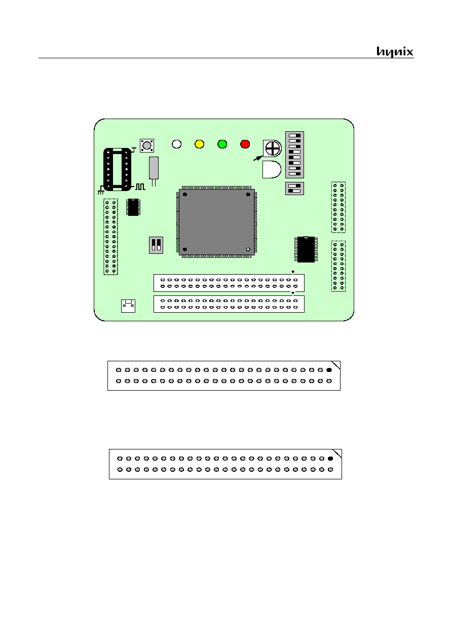
GMS
8
1
C7008/7
016
90
APR.
, 2001
Ver 2.
01
24.
2 Emul
ator
EV
A.
Board
Sett
ing
*1'
9&/4
9/&'&
&%
*1'
11&1
5(0287
+721(',
*1'
569
567
554
556
558
55:
549
547
545
543
539
537
535
533
565
563
.89
32:(5
581
6723
6/((3
CHOICE-
Dr. EVA 81C51/81
C
7
x
B/D
Rev
1.1 S/N. ----
--------
---
-B86(5%
5(6(7
-B86(5$
9B86(5
;4#+26&,
;5
25(6(7
;287
/
&'B
9
G
G
9/&
'
&
6(*79
6(*77
6(*75
6(*73
6(*6;
95(*
&2042669
&2062667
6(*65
6(*63
6(*5;
6(*59
6(*57
6(*55
6(*53
6(*4;
6(*49
6(*47
6(*45
6(*43
6(*;
6(*9
6(*7
6(*5
6(*3
6(*7:
6(*78
6(*76
6(*74
6(*6<
6(*6:
&203
&2052668
6(*66
6(*64
6(*5<
6(*5:
6(*58
6(*56
6(*54
6(*4<
6(*4:
6(*48
6(*46
6(*44
6(*<
6(*:
6(*8
6(*6
6(*4
*1'
9&/3
9&/5
&$
*1'
28B567
8B;287
*1'
56:
568
553
555
557
559
54:
548
546
544
53:
538
536
534
566
564
.89
-B86(5%
-B86(5$
1
2
3
4
5
6
7
8
1
2
ON
OF
F
SW
4
SW
5
SW
2
2
1
ON
OFF
SW
1
6XSSO
\
#.
8
9
#+
PD
[
1#
533
P$
,
VR1
+5
V
E
x
te
r
n
a
l
o
scilla
to
r
socke
t
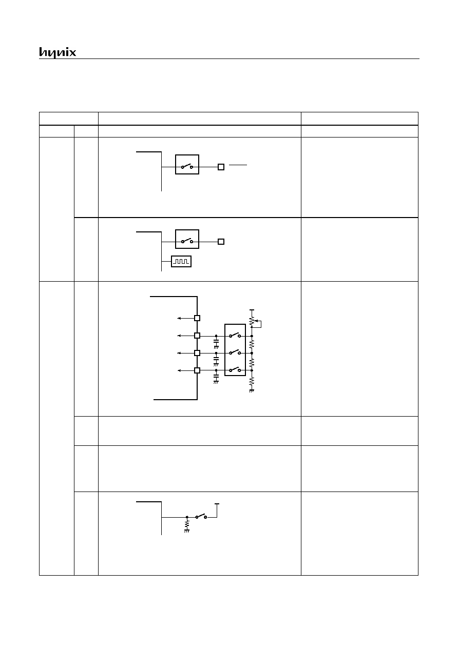
GMS81C7008/7016
APR., 2001 Ver 2.01
91
DIP Switch and VR Setting
Before execute the user program, keep in your mind the below configuration
DIP S/W, VR
Description
ON/OFF Setting
SW1
-
Emulator Reset Switch. Reset the Emulator.
Reset the Emulator.
SW2
1
Pod RESET pin configuration
Normally OFF.
EVA. chip can be reset by external
user target board.
ON : Reset is available by either
user target system board or Emula-
tor RESET switch.
OFF : Reset the MCU by Emulator
RESET switch. Does not work from
user target board.
2
Pod XOUT pin configuration
Normally OFF.
MCU XOUT pin is disconnected
internally in the Emulator. Some cir-
cumstance user may connect this
circuit.
ON : Output XOUT signal
OFF : Disconnect circuit
SW4
1
2
3
External Bias Resistors Connection
Must be ON position.
It serves the external bias resistors.
If this switches are turned off, LCD
bias voltage does not supplied,
floated because there are no inter-
nal bias resistors and bias Tr. inside
the Emulator.
4
5
6
LCD Voltage doubling circuit.
Must be OFF position.
It is reserved for the GMS81C5108.
7
Select the Stack Page.
Must be ON position.
This switch select the Stack page 0
(off) or page 1 (on).
ON : For the 81C7XXX
OFF : For the GMS81C5108
8
81Cx detect the VDD voltage but Emulator can not do because
Emulator can not operate if V
DD
is below normal opr. voltage
(5V), This switch serves LVD environment through the applying
0V to LVD pin of EVA. chip during 5V normal operation.
Position ON during normal opera-
tion.
ON : Normal operation
OFF : Force to detect the LVD, refer
to "23. POWER FAIL PROCES-
SOR" on page 87.
SW2-1
RESET pin
EVA.
Chip
SW2-2
XOUT pin
EVA.
Chip
Oscillator
VCL1
VCL2
BIAS
External Resistor
EVA. Chip Internal
VCL0
V
SS
V
DD
Adjust Contrast
SW4-1
SW4-2
SW4-3
0.47uF
×
3
10k
×
3
and Capacitor
VR1 50k
SW4
SW4-8
V
DD
EVA.
Chip
LVD pin
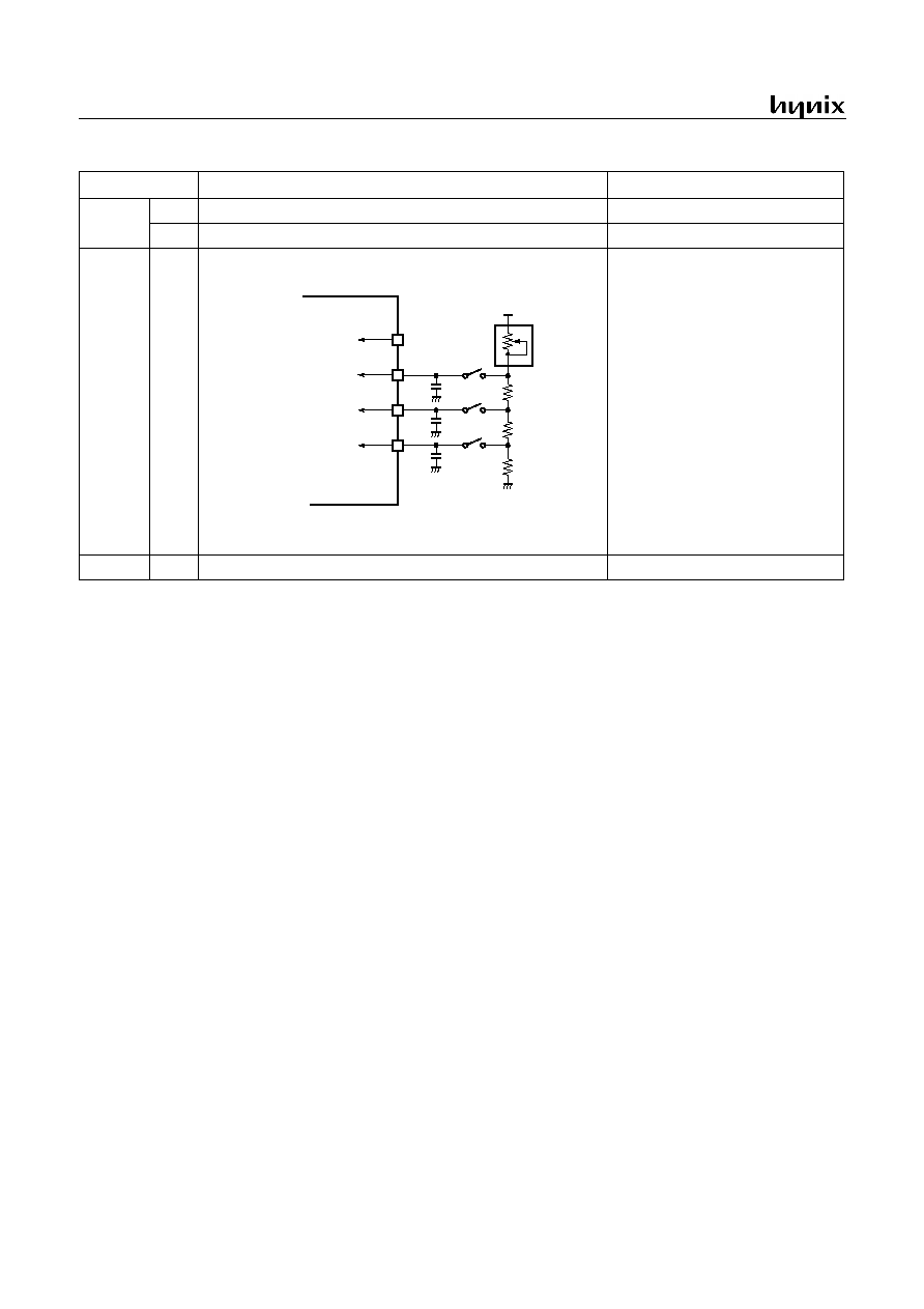
GMS81C7008/7016
92
APR., 2001 Ver 2.01
SW5
1
Internal power supply to sub-oscillation circuit.
Must be ON position.
2
Reserved for other purpose.
Must be OFF position.
VR1
-
Adjust the LCD contrast. It supply bias voltage and adjust the
VCL2 voltage.
Adjust the proper position as well as
LCD display good.
VR2
-
Reserved for other purpose.
Don't care.
DIP S/W, VR
Description
ON/OFF Setting
VCL1
VCL2
BIAS
External Resistor
EVA. Chip Internal
VCL0
V
SS
V
DD
Adjust Contrast
SW4-1
SW4-2
SW4-3
0.47uF
×
3
10k
×
3
and Capacitor
VR1
50k

APPENDIX
A. MASK ORDER SHEET
1. Customer Information
Company Name
2. Device Information
3. Marking Specification
4. Delivery Schedule
Customer Sample
Date
YYYY
MM DD
Risk Order
YYYY
MM DD
Quantity Hynix Confirmation
Application
Order Date
YYYY
MM DD
Tel: Fax:
Name &
Signature:
Package
64SDIP 64MQFP
5. ROM Code Verification
Verification D ate:
YYYY
MM DD
Approval Date:
YYYY
MM DD
Please confirm our verification data.
I agree w ith your verification data and confirm
you to m ake m ask set.
Check Sum:
Tel: Fax:
Name &
Signature:
Tel: Fax:
Name &
Signature:
C000
H
E000
H
FFFF
H
.OTP file data
DFFF
H
Mask Data
Internet
File Name: ( .OTP)
(Please check mark into )
pcs
pcs
Check Sum: ( )
Customer should write inside thick line box.
This box is written after "5.Verification".
R C O SC O pt.
Crystal RC
GMS
81C
701
6 (1
6K
R
O
M)
GM
S
8
1C
7008 (8K
R
O
M)
ROM Size
8K 16K
YYWW KOREA
Customer's logo
Customer logo is not required.
YYWW KOREA
GMS81C70
Customer's part number
If the customer logo must be used in the special mark, please submit a clean original of the logo.
08 or 16
E-mail:
E-mail:
01-APR-2001
MASK ORDER & VERIFICATION SHEET
GMS81C7008
-LA
GMS81C7016
-LA
GMS81C70
-LA
Lot Number
Hynix ROM Code
Number
GMS81C71XX LCD MCU APPENDIX
APR. 2001 Ver 2.01
ii
B. INSTRUCTION
B.1 Terminology List
Terminology
Description
A
Accumulator
X
X - register
Y
Y - register
PSW
Program Status Word
#imm
8-bit Immediate data
dp
Direct Page Offset Address
!abs
Absolute Address
[ ]
Indirect expression
{ }
Register Indirect expression
{ }+
Register Indirect expression, after that, Register auto-increment
.bit
Bit Position
A.bit
Bit Position of Accumulator
dp.bit
Bit Position of Direct Page Memory
M.bit
Bit Position of Memory Data (000
H
~0FFF
H
)
rel
Relative Addressing Data
upage
U-page (0FF00
H
~0FFFF
H
) Offset Address
n
Table CALL Number (0~15)
+
Addition
x
Upper Nibble Expression in Opcode
y
Upper Nibble Expression in Opcode
-
Subtraction
×
Multiplication
/
Division
( )
Contents Expression
AND
OR
Exclusive OR
~
NOT
Assignment / Transfer / Shift Left
Shift Right
Exchange
=
Equal
Not Equal
0
Bit Position
1
Bit Position
GMS81C71XX LCD MCU APPENDIX
iii
APR. 2001 Ver 2.01
B.2 Instruction Map
LOW
HIGH
00000
00
00001
01
00010
02
00011
03
00100
04
00101
05
00110
06
00111
07
01000
08
01001
09
01010
0A
01011
0B
01100
0C
01101
0D
01110
0E
01111
0F
000
-
SET1
dp.bit
BBS
A.bit,rel
BBS
dp.bit,rel
ADC
#imm
ADC
dp
ADC
dp+X
ADC
!abs
ASL
A
ASL
dp
TCALL
0
SETA1
.bit
BIT
dp
POP
A
PUSH
A
BRK
001
CLRC
SBC
#imm
SBC
dp
SBC
dp+X
SBC
!abs
ROL
A
ROL
dp
TCALL
2
CLRA1
.bit
COM
dp
POP
X
PUSH
X
BRA
rel
010
CLRG
CMP
#imm
CMP
dp
CMP
dp+X
CMP
!abs
LSR
A
LSR
dp
TCALL
4
NOT1
M.bit
TST
dp
POP
Y
PUSH
Y
PCALL
Upage
011
DI
OR
#imm
OR
dp
OR
dp+X
OR
!abs
ROR
A
ROR
dp
TCALL
6
OR1
OR1B
CMPX
dp
POP
PSW
PUSH
PSW
RET
100
CLRV
AND
#imm
AND
dp
AND
dp+X
AND
!abs
INC
A
INC
dp
TCALL
8
AND1
AND1B
CMPY
dp
CBNE
dp+X
TXSP
INC
X
101
SETC
EOR
#imm
EOR
dp
EOR
dp+X
EOR
!abs
DEC
A
DEC
dp
TCALL
10
EOR1
EOR1B
DBNE
dp
XMA
dp+X
TSPX
DEC
X
110
SETG
LDA
#imm
LDA
dp
LDA
dp+X
LDA
!abs
TXA
LDY
dp
TCALL
12
LDC
LDCB
LDX
dp
LDX
dp+Y
XCN
DAS
111
EI
LDM
dp,#imm
STA
dp
STA
dp+X
STA
!abs
TAX
STY
dp
TCALL
14
STC
M.bit
STX
dp
STX
dp+Y
XAX
STOP
LOW
HIGH
10000
10
10001
11
10010
12
10011
13
10100
14
10101
15
10110
16
10111
17
11000
18
11001
19
11010
1A
11011
1B
11100
1C
11101
1D
11110
1E
11111
1F
000
BPL
rel
CLR1
dp.bit
BBC
A.bit,rel
BBC
dp.bit,rel
ADC
{X}
ADC
!abs+Y
ADC
[dp+X]
ADC
[dp]+Y
ASL
!abs
ASL
dp+X
TCALL
1
JMP
!abs
BIT
!abs
ADDW
dp
LDX
#imm
JMP
[!abs]
001
BVC
rel
SBC
{X}
SBC
!abs+Y
SBC
[dp+X]
SBC
[dp]+Y
ROL
!abs
ROL
dp+X
TCALL
3
CALL
!abs
TEST
!abs
SUBW
dp
LDY
#imm
JMP
[dp]
010
BCC
rel
CMP
{X}
CMP
!abs+Y
CMP
[dp+X]
CMP
[dp]+Y
LSR
!abs
LSR
dp+X
TCALL
5
MUL
TCLR1
!abs
CMPW
dp
CMPX
#imm
CALL
[dp]
011
BNE
rel
OR
{X}
OR
!abs+Y
OR
[dp+X]
OR
[dp]+Y
ROR
!abs
ROR
dp+X
TCALL
7
DBNE
Y
CMPX
!abs
LDYA
dp
CMPY
#imm
RETI
100
BMI
rel
AND
{X}
AND
!abs+Y
AND
[dp+X]
AND
[dp]+Y
INC
!abs
INC
dp+X
TCALL
9
DIV
CMPY
!abs
INCW
dp
INC
Y
TAY
101
BVS
rel
EOR
{X}
EOR
!abs+Y
EOR
[dp+X]
EOR
[dp]+Y
DEC
!abs
DEC
dp+X
TCALL
11
XMA
{X}
XMA
dp
DECW
dp
DEC
Y
TYA
110
BCS
rel
LDA
{X}
LDA
!abs+Y
LDA
[dp+X]
LDA
[dp]+Y
LDY
!abs
LDY
dp+X
TCALL
13
LDA
{X}+
LDX
!abs
STYA
dp
XAY
DAA
111
BEQ
rel
STA
{X}
STA
!abs+Y
STA
[dp+X]
STA
[dp]+Y
STY
!abs
STY
dp+X
TCALL
15
STA
{X}+
STX
!abs
CBNE
dp
XYX
NOP
GMS81C71XX LCD MCU APPENDIX
APR. 2001 Ver 2.01
iv
B.3 Instruction Set
Arithmetic / Logic Operation
No.
Mnemonic
Op
Code
Byte
No
Cycle
No
Operation
Flag
NVGBHIZC
1
ADC #imm
04
2
2
Add with carry.
2
ADC dp
05
2
3
A
( A ) + ( M ) + C
3
ADC dp + X
06
2
4
4
ADC !abs
07
3
4
NV--H-ZC
5
ADC !abs + Y
15
3
5
6
ADC [ dp + X ]
16
2
6
7
ADC [ dp ] + Y
17
2
6
8
ADC { X }
14
1
3
9
AND #imm
84
2
2
Logical AND
10
AND dp
85
2
3
A
( A )
( M )
11
AND dp + X
86
2
4
12
AND !abs
87
3
4
N-----Z-
13
AND !abs + Y
95
3
5
14
AND [ dp + X ]
96
2
6
15
AND [ dp ] + Y
97
2
6
16
AND { X }
94
1
3
17
ASL A
08
1
2
Arithmetic shift left
18
ASL dp
09
2
4
N-----ZC
19
ASL dp + X
19
2
5
20
ASL !abs
18
3
5
21
CMP #imm
44
2
2
Compare accumulator contents with memory contents
( A ) - ( M )
22
CMP dp
45
2
3
23
CMP dp + X
46
2
4
24
CMP !abs
47
3
4
N-----ZC
25
CMP !abs + Y
55
3
5
26
CMP [ dp + X ]
56
2
6
27
CMP [ dp ] + Y
57
2
6
28
CMP { X }
54
1
3
29
CMPX #imm
5E
2
2
Compare X contents with memory contents
30
CMPX dp
6C
2
3
( X ) - ( M )
N-----ZC
31
CMPX !abs
7C
3
4
32
CMPY #imm
7E
2
2
Compare Y contents with memory contents
33
CMPY dp
8C
2
3
( Y ) - ( M )
N-----ZC
34
CMPY !abs
9C
3
4
35
COM dp
2C
2
4
1'S Complement : ( dp )
~( dp )
N-----Z-
36
DAA
DF
1
3
Decimal adjust for addition
N-----ZC
37
DAS
CF
1
3
Decimal adjust for subtraction
N-----ZC
38
DEC A
A8
1
2
Decrement
N-----Z-
39
DEC dp
A9
2
4
M
( M ) - 1
N-----Z-
40
DEC dp + X
B9
2
5
N-----Z-
41
DEC !abs
B8
3
5
N-----Z-
42
DEC X
AF
1
2
N-----Z-
43
DEC Y
BE
1
2
N-----Z-
7 6 5 4 3 2 1 0
"0"
C
GMS81C71XX LCD MCU APPENDIX
v
APR. 2001 Ver 2.01
44
DIV
9B
1
12
Divide : YA / X Q: A, R: Y
NV--H-Z-
45
EOR #imm
A4
2
2
Exclusive OR
46
EOR dp
A5
2
3
A
( A )
( M )
47
EOR dp + X
A6
2
4
48
EOR !abs
A7
3
4
N-----Z-
49
EOR !abs + Y
B5
3
5
50
EOR [ dp + X ]
B6
2
6
51
EOR [ dp ] + Y
B7
2
6
52
EOR { X }
B4
1
3
53
INC A
88
1
2
Increment
N-----ZC
54
INC dp
89
2
4
M
( M ) + 1
N-----Z-
55
INC dp + X
99
2
5
N-----Z-
56
INC !abs
98
3
5
N-----Z-
57
INC X
8F
1
2
N-----Z-
58
INC Y
9E
1
2
N-----Z-
59
LSR A
48
1
2
Logical shift right
60
LSR dp
49
2
4
N-----ZC
61
LSR dp + X
59
2
5
62
LSR !abs
58
3
5
63
MUL
5B
1
9
Multiply : YA
Y
×
A
N-----Z-
64
OR #imm
64
2
2
Logical OR
65
OR dp
65
2
3
A
( A )
( M )
66
OR dp + X
66
2
4
67
OR !abs
67
3
4
N-----Z-
68
OR !abs + Y
75
3
5
69
OR [ dp + X ]
76
2
6
70
OR [ dp ] + Y
77
2
6
71
OR { X }
74
1
3
72
ROL A
28
1
2
Rotate left through Carry
73
ROL dp
29
2
4
N-----ZC
74
ROL dp + X
39
2
5
75
ROL !abs
38
3
5
76
ROR A
68
1
2
Rotate right through Carry
77
ROR dp
69
2
4
N-----ZC
78
ROR dp + X
79
2
5
79
ROR !abs
78
3
5
80
SBC #imm
24
2
2
Subtract with Carry
81
SBC dp
25
2
3
A
( A ) - ( M ) - ~( C )
82
SBC dp + X
26
2
4
83
SBC !abs
27
3
4
NV--HZC
84
SBC !abs + Y
35
3
5
85
SBC [ dp + X ]
36
2
6
86
SBC [ dp ] + Y
37
2
6
87
SBC { X }
34
1
3
88
TST dp
4C
2
3
Test memory contents for negative or zero, ( dp ) - 00
H
N-----Z-
89
XCN
CE
1
5
Exchange nibbles within the accumulator
A
7
~A
4
A
3
~A
0
N-----Z-
No.
Mnemonic
Op
Code
Byte
No
Cycle
No
Operation
Flag
NVGBHIZC
7 6 5 4 3 2 1 0
"0"
C
7 6 5 4 3 2 1 0
C
7 6 5 4 3 2 1 0
C
GMS81C71XX LCD MCU APPENDIX
APR. 2001 Ver 2.01
vi
Register / Memory Operation
No.
Mnemonic
Op
Code
Byte
No
Cycle
No
Operation
Flag
NVGBHIZC
1
LDA #imm
C4
2
2
Load accumulator
2
LDA dp
C5
2
3
A
( M )
3
LDA dp + X
C6
2
4
4
LDA !abs
C7
3
4
5
LDA !abs + Y
D5
3
5
N-----Z-
6
LDA [ dp + X ]
D6
2
6
7
LDA [ dp ] + Y
D7
2
6
8
LDA { X }
D4
1
3
9
LDA { X }+
DB
1
4
X- register auto-increment : A
( M ) , X
X + 1
10
LDM dp,#imm
E4
3
5
Load memory with immediate data : ( M )
imm
--------
11
LDX #imm
1E
2
2
Load X-register
12
LDX dp
CC
2
3
X
( M )
N-----Z-
13
LDX dp + Y
CD
2
4
14
LDX !abs
DC
3
4
15
LDY #imm
3E
2
2
Load Y-register
16
LDY dp
C9
2
3
Y
( M )
N-----Z-
17
LDY dp + X
D9
2
4
18
LDY !abs
D8
3
4
19
STA dp
E5
2
4
Store accumulator contents in memory
20
STA dp + X
E6
2
5
( M )
A
21
STA !abs
E7
3
5
22
STA !abs + Y
F5
3
6
--------
23
STA [ dp + X ]
F6
2
7
24
STA [ dp ] + Y
F7
2
7
25
STA { X }
F4
1
4
26
STA { X }+
FB
1
4
X- register auto-increment : ( M )
A, X
X + 1
27
STX dp
EC
2
4
Store X-register contents in memory
28
STX dp + Y
ED
2
5
( M )
X
--------
29
STX !abs
FC
3
5
30
STY dp
E9
2
4
Store Y-register contents in memory
31
STY dp + X
F9
2
5
( M )
Y
--------
32
STY !abs
F8
3
5
33
TAX
E8
1
2
Transfer accumulator contents to X-register : X
A
N-----Z-
34
TAY
9F
1
2
Transfer accumulator contents to Y-register : Y
A
N-----Z-
35
TSPX
AE
1
2
Transfer stack-pointer contents to X-register : X
sp
N-----Z-
36
TXA
C8
1
2
Transfer X-register contents to accumulator: A
X
N-----Z-
37
TXSP
8E
1
2
Transfer X-register contents to stack-pointer: sp
X
N-----Z-
38
TYA
BF
1
2
Transfer Y-register contents to accumulator: A
Y
N-----Z-
39
XAX
EE
1
4
Exchange X-register contents with accumulator :X
A
--------
40
XAY
DE
1
4
Exchange Y-register contents with accumulator :Y
A
--------
41
XMA dp
BC
2
5
Exchange memory contents with accumulator
42
XMA dp+X
AD
2
6
( M )
A
N-----Z-
43
XMA {X}
BB
1
5
44
XYX
FE
1
4
Exchange X-register contents with Y-register : X
Y
--------
GMS81C71XX LCD MCU APPENDIX
vii
APR. 2001 Ver 2.01
16-BIT operation
Bit Manipulation
No.
Mnemonic
Op
Code
Byte
No
Cycle
No
Operation
Flag
NVGBHIZC
1
ADDW dp
1D
2
5
16-Bits add without Carry
YA
( YA ) ( dp +1 ) ( dp )
NV--H-ZC
2
CMPW dp
5D
2
4
Compare YA contents with memory pair contents :
(YA)
-
(dp+1)(dp)
N-----ZC
3
DECW dp
BD
2
6
Decrement memory pair
( dp+1)( dp)
( dp+1) ( dp) - 1
N-----Z-
4
INCW dp
9D
2
6
Increment memory pair
( dp+1) ( dp)
( dp+1) ( dp ) + 1
N-----Z-
5
LDYA dp
7D
2
5
Load YA
YA
( dp +1 ) ( dp )
N-----Z-
6
STYA dp
DD
2
5
Store YA
( dp +1 ) ( dp )
YA
--------
7
SUBW dp
3D
2
5
16-Bits subtract without carry
YA
( YA ) - ( dp +1) ( dp)
NV--H-ZC
No.
Mnemonic
Op
Code
Byte
No
Cycle
No
Operation
Flag
NVGBHIZC
1
AND1 M.bit
8B
3
4
Bit AND C-flag : C
( C )
( M .bit )
-------C
2
AND1B M.bit
8B
3
4
Bit AND C-flag and NOT : C
( C )
~( M .bit )
-------C
3
BIT dp
0C
2
4
Bit test A with memory :
MM----Z-
4
BIT !abs
1C
3
5
Z
( A )
( M ) , N
( M
7
) , V
( M
6
)
5
CLR1 dp.bit
y1
2
4
Clear bit : ( M.bit )
"0"
--------
6
CLRA1 A.bit
2B
2
2
Clear A bit : ( A.bit )
"0"
--------
7
CLRC
20
1
2
Clear C-flag : C
"0"
-------0
8
CLRG
40
1
2
Clear G-flag : G
"0"
--0-----
9
CLRV
80
1
2
Clear V-flag : V
"0"
-0--0---
10
EOR1 M.bit
AB
3
5
Bit exclusive-OR C-flag : C
( C )
( M .bit )
-------C
11
EOR1B M.bit
AB
3
5
Bit exclusive-OR C-flag and NOT : C
( C )
~(M .bit)
-------C
12
LDC M.bit
CB
3
4
Load C-flag : C
( M .bit )
-------C
13
LDCB M.bit
CB
3
4
Load C-flag with NOT : C
~( M .bit )
-------C
14
NOT1 M.bit
4B
3
5
Bit complement : ( M .bit )
~( M .bit )
--------
15
OR1 M.bit
6B
3
5
Bit OR C-flag : C
( C )
( M .bit )
-------C
16
OR1B M.bit
6B
3
5
Bit OR C-flag and NOT : C
( C )
~( M .bit )
-------C
17
SET1 dp.bit
x1
2
4
Set bit : ( M.bit )
"1"
--------
18
SETA1 A.bit
0B
2
2
Set A bit : ( A.bit )
"1"
--------
19
SETC
A0
1
2
Set C-flag : C
"1"
-------1
20
SETG
C0
1
2
Set G-flag : G
"1"
--1-----
21
STC M.bit
EB
3
6
Store C-flag : ( M .bit )
C
--------
22
TCLR1 !abs
5C
3
6
Test and clear bits with A :
A - ( M ) , ( M )
( M )
~( A )
N-----Z-
23
TSET1 !abs
3C
3
6
Test and set bits with A :
A - ( M ) , ( M )
( M )
( A )
N-----Z-
GMS81C71XX LCD MCU APPENDIX
APR. 2001 Ver 2.01
viii
Branch / Jump Operation
No.
Mnemonic
Op
Code
Byte
No
Cycle
No
Operation
Flag
NVGBHIZC
1
BBC A.bit,rel
y2
2
4/6
Branch if bit clear :
--------
2
BBC dp.bit,rel
y3
3
5/7
if ( bit ) = 0 , then pc
( pc ) + rel
3
BBS A.bit,rel
x2
2
4/6
Branch if bit set :
--------
4
BBS dp.bit,rel
x3
3
5/7
if ( bit ) = 1 , then pc
( pc ) + rel
5
BCC rel
50
2
2/4
Branch if carry bit clear
if ( C ) = 0 , then pc
( pc ) + rel
--------
6
BCS rel
D0
2
2/4
Branch if carry bit set
if ( C ) = 1 , then pc
( pc ) + rel
--------
7
BEQ rel
F0
2
2/4
Branch if equal
if ( Z ) = 1 , then pc
( pc ) + rel
--------
8
BMI rel
90
2
2/4
Branch if minus
if ( N ) = 1 , then pc
( pc ) + rel
--------
9
BNE rel
70
2
2/4
Branch if not equal
if ( Z ) = 0 , then pc
( pc ) + rel
--------
10
BPL rel
10
2
2/4
Branch if plus
if ( N ) = 0 , then pc
( pc ) + rel
--------
11
BRA rel
2F
2
4
Branch always
pc
( pc ) + rel
--------
12
BVC rel
30
2
2/4
Branch if overflow bit clear
if (V) = 0 , then pc
( pc) + rel
--------
13
BVS rel
B0
2
2/4
Branch if overflow bit set
if (V) = 1 , then pc
( pc ) + rel
--------
14
CALL !abs
3B
3
8
Subroutine call
15
CALL [dp]
5F
2
8
M( sp)
( pc
H
), sp
sp - 1, M(sp)
(pc
L
), sp
sp - 1,
if !abs, pc
abs ; if [dp], pc
L
( dp ), pc
H
( dp+1 ) .
--------
16
CBNE dp,rel
FD
3
5/7
Compare and branch if not equal :
--------
17
CBNE dp+X,rel
8D
3
6/8
if ( A )
( M ) , then pc
( pc ) + rel.
18
DBNE dp,rel
AC
3
5/7
Decrement and branch if not equal :
--------
19
DBNE Y,rel
7B
2
4/6
if ( M )
0 , then pc
( pc ) + rel.
20
JMP !abs
1B
3
3
Unconditional jump
21
JMP [!abs]
1F
3
5
pc
jump address
--------
22
JMP [dp]
3F
2
4
23
PCALL upage
4F
2
6
U-page call
M(sp)
( pc
H
), sp
sp - 1, M(sp)
( pc
L
),
sp
sp - 1, pc
L
( upage ), pc
H
"0FF
H
" .
--------
24
TCALL n
nA
1
8
Table call : (sp)
( pc
H
), sp
sp - 1,
M(sp)
( pc
L
),sp
sp - 1,
pc
L
(Table vector L), pc
H
(Table vector H)
--------
GMS81C71XX LCD MCU APPENDIX
ix
APR. 2001 Ver 2.01
Control Operation & Etc.
No.
Mnemonic
Op
Code
Byte
No
Cycle
No
Operation
Flag
NVGBHIZC
1
BRK
0F
1
8
Software interrupt : B
"1", M(sp)
(pc
H
), sp
sp-1,
M(s)
(pc
L
), sp
sp - 1, M(sp)
(PSW), sp
sp -1,
pc
L
( 0FFDE
H
) , pc
H
( 0FFDF
H
) .
---1-0--
2
DI
60
1
3
Disable all interrupts : I
"0"
-----0--
3
EI
E0
1
3
Enable all interrupt : I
"1"
-----1--
4
NOP
FF
1
2
No operation
--------
5
POP A
0D
1
4
sp
sp + 1, A
M( sp )
6
POP X
2D
1
4
sp
sp + 1, X
M( sp )
--------
7
POP Y
4D
1
4
sp
sp + 1, Y
M( sp )
8
POP PSW
6D
1
4
sp
sp + 1, PSW
M( sp )
restored
9
PUSH A
0E
1
4
M( sp )
A , sp
sp - 1
10
PUSH X
2E
1
4
M( sp )
X , sp
sp - 1
--------
11
PUSH Y
4E
1
4
M( sp )
Y , sp
sp - 1
12
PUSH PSW
6E
1
4
M( sp )
PSW , sp
sp - 1
13
RET
6F
1
5
Return from subroutine
sp
sp +1, pc
L
M( sp ), sp
sp +1, pc
H
M( sp )
--------
14
RETI
7F
1
6
Return from interrupt
sp
sp +1, PSW
M( sp ), sp
sp + 1,
pc
L
M( sp ), sp
sp + 1, pc
H
M( sp )
restored
15
STOP
EF
1
3
Stop mode ( halt CPU, stop oscillator )
--------

GMS81C71XX LCD MCU APPENDIX
APR. 2001 Ver 2.01
x
C. SOFTWARE EXAMPLE
;*****************************************************************************
; Title: GMS81C7016 (GMS800 Series) Demonstration Program *
; Company: Hynix semiconductor Inc. *
; Contents: LCD DISPLAY & DUAL THERMOMETER *
;*****************************************************************************
;
;******** DEFINE I/O PORT & FUNCTION REGISTER ADDRESS *********
;
R0 EQU 0C0H ;port R0 register
R1 EQU 0C1H ;port R1 register
R2 EQU 0C2H ;port R2 register
R3 EQU 0C3H ;port R3 register
R4 EQU 0C4H ;port R4 register
R5 EQU 0C5H ;port R5 register
;
R0DD EQU 0C8H ;port R0 data I/O direction register
R1DD EQU 0C9H ;port R1 data I/O direction register
R2DD EQU 0CAH ;port R2 data I/O direction register
R3DD EQU 0CBH ;port R3 data I/O direction register
R4DD EQU 0CCH ;port R4 data I/O direction register
R5DD EQU 0CDH ;port R5 data I/O direction register
;
R0PU EQU 0D0H ;port R0 Pull-up selection register
R1PU EQU 0D1H ;port R1 Pull-up selection register
R2PU EQU 0D2H ;port R2 Pull-up selection register
R3PU EQU 0D3H ;port R3 Pull-up selection register
;
R0CR EQU 0D4H ;port R0 Type selection register
R1CR EQU 0D5H ;port R1 Type selection register
R2CR EQU 0D6H ;port R2 Type selection register
R3CR EQU 0D7H ;port R3 Type selection register
;
IEDS EQU 0D8H ;External interrupt edge selection register
PMR EQU 0D9H ;Alternative port mode register
IENL EQU 0DAH ;int. enable register low
IENH EQU 0DBH ;int. enable register high
IRQL EQU 0DCH ;int. request flag register low
IRQH EQU 0DDH ;int. request flag register high
SLPR EQU 0DEH ;sleep mode register
WDTR EQU 0DFH ;Watchdog timer register
TM0 EQU 0E0H ;Timer 0 mode register
TDR0 EQU 0E1H ;Timer 0 data register
TM1 EQU 0E2H ;Timer 1 mode register
TDR1 EQU 0E3H ;Timer 1 data register
T1PPR EQU 0E3H ;PWM0 period register
T1PDR EQU 0E4H ;Timer 1 pulse duty register
PWM0HR EQU 0E5H ;PWM0 high register
TM2 EQU 0E6H ;Timer 2 mode register
TDR2 EQU 0E7H ;Timer 2 data register
TM3 EQU 0E8H ;Timer 3 mode register
TDR3 EQU 0E9H ;Timer 3 data register
T3PPR EQU 0E9H ;PWM1 period register
T3PDR EQU 0EAH ;Timer 3 pulse duty register
PWM1HR EQU 0EBH ;PWM1 high register
ADCM EQU 0ECH ;ADC mode register
ADR EQU 0EDH ;ADC result data register
WTMR EQU 0EFH ;Watch timer mode register
KSMR EQU 0F0H ;Key scan mode register
LCDM EQU 0F1H ;LCD mode register
LCDPM EQU 0F2H ;LCD port mode register
RPR EQU 0F3H ;RAM paging register
BITR EQU 0F4H ;Basic interval timer data register
CKCTLR EQU 0F4H ;Clock control register
SCMR EQU 0F5H ;System clock mode register
PFDR EQU 0FBH ;Power fail detector
BUR EQU 0FDH ;buzzer data register
SMR EQU 0FEH ;Serial mode register
SIOD EQU 0FFH ;Serial data buffer register
;
;*********** MACRO DEFINITION ************
;
R_SAVEMACRO ;Save Registers to Stacks

GMS81C71XX LCD MCU APPENDIX
xi
APR. 2001 Ver 2.01
PUSH A
PUSH X
PUSH Y
ENDM
;
R_RSTRMACRO ;Restore Register from Stacks
POP Y
POP X
POP A
ENDM
;
;*********** CONSTANT DEFINITION ***********
;
;
;
;**************************************************************************
; RAM ALLOCATION *
;**************************************************************************
TEMP0 DS 1
TEMP1 DS 1
TEMP2 DS 1
FLAG1 DS 1
RPTEN EQU 1,FLAG1 ;SET RPTEN(REPEAT KEY ENABLE) AFTER 1 SEC.
KEYONF EQU 2,FLAG1 ;KEYSCAN
ACTKEY EQU 3,FLAG1 ;AT ONCE, KEY VALID
TOGMO3 EQU 4,FLAG1 ;MODE 3 (PORT TOGGLE)
DUAL_T EQU 5,FLAG1 ;INSIDE & OUTSIDE TEMP. DUAL DISPLAY
OUTSIDE EQU 6,FLAG1 ;INSIDE TEMP or OUTSIDE TEMP.
FLAG2 DS 1
F200MS EQU 0,FLAG2
F20MS EQU 1,FLAG2
F_1MIN EQU 2,FLAG2 ;WTIMER
LPM EQU 3,FLAG2 ;LEFT TIME PM FLAG
RPM EQU 4,FLAG2 ;RIGHT TIME PM FLAG
STATUS DS 1
RPTKEY EQU 7,STATUS
F_CLOCK EQU 6,STATUS
F_ON EQU 0,STATUS
DISPSIGN DS 1
DISPRAM DS 1 ;TEMP.
DISPRAM1 DS 4 ;LEFT TIME, RIGHT TIME
ONDO DS 2
LHOUR DS 1 ;LEFT WATCH COUNT
LMINUTE DS 1
RHOUR DS 1
RMINUTE DS 1 ;RIGHT WATCH COUNT BUF.
TIMESET DS 4 ;WATCH SET BUFFER
TSFLAG DS 1
TSLPM EQU 0,TSFLAG ;TIME SET LEFT PM
TSRPM EQU 1,TSFLAG ;TIME SET RIGHT PM
BLINKCNT DS 1 ;BLINK COUNTER 0~250 LOOP
;
NEWKY DS 1
OLDKY DS 1
PORTDT DS 1
KEYNM DS 1
KEYDT DS 1
TOTLKY DS 1
CHATFL DS 1
R0BUF DS 1
DGTCNT DS 1
MODE DS 1
SUBMODE DS 1
BSCTIME DS 1
TEMPCNT DS 1
HZCNT DS 1
PWMF DS 1
PERIOD EQU 0,PWMF
;
;**************************************************************************
; INTERRUPT VECTOR TABLE *
;**************************************************************************

GMS81C71XX LCD MCU APPENDIX
APR. 2001 Ver 2.01
xii
;
ORG 0FFE0H
DW NOT_USED ; Timer-3
DW NOT_USED ; Timer-2
DW WTIMER ; Watch Timer
DW INT_AD ; A/D CON.
DW NOT_USED ; Serial I/O
DW NOT_USED ; Not used
DW NOT_USED ; Not used
DW NOT_USED ; Int.2
DW TIMER1 ; Timer-1
DW TIMER0 ; Timer-0
DW INT1 ; Int.1
DW INT0 ; Int.0
DW NOT_USED; Watch Dog Timer
DW NOT_USED; BIT
DW INT_KEY ; Key Scan
DW RESET ; Reset
;
;**************************************************************************
; MAIN PROGRAM *
;**************************************************************************
;
ORG 0C000H ;Program Start Address
;ORG 0E000H ; 8K ROM VERSION
;
RESET: LDM WDTR,#0
LDM RPR,#1
;
CLRG
LDX #0
RAMCLR: LDA #0 ;RAM Clear(!0000H->!00BFH)
STA {X}+ ;M(X) <- A, then X <- X+1
CMPX #0C0H ;X = #0C0H ?
BNE RAMCLR
SETG
LDX #0
RAMCLR1: LDA #0 ;RAM Clear(!0100H->!011AH)
STA {X}+ ;M(X) <- A, then X <- X+1
CMPX #1BH ;X = #01BH ?
BNE RAMCLR1
CLRG
;
LDX #0FFH ;Stack Pointer Initial
TXSP ;SP. <- #0FFH
;
;******** USER RAM INITIALIZE **********
;
; LDM MODE,#4
; LDM SUBMODE,#1
SET1 LPM ;KST PM 12:00 JUST NOON
LDM LHOUR,#12H
LDM LMINUTE,#00H
LDM RHOUR,#03H ;UTC AM 03:00
LDM RMINUTE,#00H
SET1 OUTSIDE
SET1 F_ON ;POWER ON
;
;********** PORT INITIALIZE ************
;
LDM LCDPM,#0 ;SEG0~SEG23 are used
LDM R0,#0 ;I/O Port Data Clea
LDM R1,#0 ;I/O Port Data Clear
LDM R2,#0
LDM R3,#0
LDM R0DD,#1111_0001B ;R05,R06,R07: output for Keyscan
LDM R1DD,#0000_0000B
LDM R2DD,#0000_0000B ;R20~R23: input for keyscan
LDM R3DD,#0000_0100B
LDM R2PU,#0000_1111B ;R20~R23 pull-up active
;
;***** CONTROL REGISTER INITIALIZE *****
;
LDM CKCTLR,#0 ;WAKE UP TIME = 0.0625 sec
;(1/32768)*8*256 = 0.0625sec
LDM TDR0,#249 ;8us x (249+1) = 2ms
LDM TM0,#0000_1111B ;8BIT Timer,8us,Start Count-up
LDM TDR1,#249 ;2us x (249+1) = 500us
LDM TM1,#0000_1111B ;Timer1(8bit),32us,Start Count-up
LDM TM3,#1010_1011B

GMS81C71XX LCD MCU APPENDIX
xiii
APR. 2001 Ver 2.01
LDM T3PPR,#99
LDM T3PDR,#50
LDM PWM1HR,#00H
LDM PMR,#80H
LDM IRQH,#0 ;Clear All Interrupts Requeat Flags
LDM IRQL,#0
LDM IENL,#1111_1111B ;INT2,ADC,WT,T2,T3
LDM IENH,#1111_1111B ;BIT,WDT,INT0,INT1,T0,T1
LDM IEDS,#0001_0101B ;External Int. Falling edge select
LDM KSMR,#0000_0001B ;R10 KEY INTERRUPT
LDM WTMR,#48H ;ENABLE WT COUNTER, 2Hz, SELECT SUBCLOCK
LDM LCDM,#70H ;CLK=fsub/64, 1/4duty, internal Bias
LDM SCMR,#0 ;1/2, MAIN OSC.
EI ;Enable Interrupts
;
LOOP: BBC KEYONF,EXE1 ;TEST IF KEY IS PRESSED
CALL KEYDECODE
CLR1 KEYONF ;CLEAR KEY FLAG
EXE1:
BBC F20MS,NEXT1
CLR1 F20MS
;
;*****EVERY 20MS*****
;
CALL MODEEXE ;SETTING DISPLAY MEMORY
CALL MODE1EXE ;DURING CLOCK,
CALL MODE3EXE
CALL LCDDGT ;7-Segments Display
CALL LCDDOT ;Dot Display
CALL ADCEXE ;ADC execution
CALL LKEYSCAN
NEXT1:
BBC F200MS,ELOOP
CLR1 F200MS
;
;*****EVERY 200MS*****
;
CALL WIND
ELOOP:
BBS F_ON,EXE2
CLR1 R0.7 ;FOR WAKE-UP BY NEXT KEY
CLR1 R0.6 ;FOR WAKE-UP BY NEXT KEY
CLR1 R0.5 ;FOR WAKE-UP BY NEXT KEY
CLR1 R0.4 ;FOR WAKE-UP BY NEXT KEY
STOP
NOP
NOP
IF [F_1MIN]
CLR1 F_1MIN
CALL MODEEXE
CALL LCDDGT ;7-Segments Display
CALL LCDDOT ;Dot Display
ENDIF
CALL LKEYSCAN
EXE2:
JMP LOOP
;
;**************************************************************************
; TIMER0,INTERRUPT ROUTINE(2ms) *
;**************************************************************************
;
TIMER0: R_SAVE ;Save Registers to Stacks
CLRG
CALL MAKE10MS ;SET every 10ms
R_RSTR ;Restore Registers from Stacks
RETI
;
;**************************************************************************
; TIMER1 *
;**************************************************************************
;
TIMER1: R_SAVE
CLRG
R_RSTR

GMS81C71XX LCD MCU APPENDIX
APR. 2001 Ver 2.01
xiv
RETI
;
;**************************************************************************
; WATCH TIMER 4Hz *
;**************************************************************************
;
WTIMER: R_SAVE
CLRG
NOT1 R0.0
INC HZCNT
LDA HZCNT
CMP #120
BNE WT5
LDM HZCNT,#0
SET1 F_1MIN
CALL INC1MIN
WT5: R_RSTR
RETI
;
;**************************************************************************
; PORT INTERRUPT *
;**************************************************************************
;
INT_KEY: R_SAVE
CLRG
BBS CHATFL.7,IK8
BBS F_ON,IK8
LDX #3
LDM KSMR,#0 ;MAKE R10 TO BE NORMAL INPUT
WW: LDY #2 ;24ms wait
WW2: LDA #8
WW3: DEC A
BNE WW3
DEC Y
BNE WW2
LDA R1 ;READ R10
ROR A
BCS IK8
DEC X
BNE WW
LDM SCMR,#0 ;MAIN OSC.
SET1 F_ON
SET1 CHATFL.7
LDM OLDKY,#0CH
IK8: LDM KSMR,#1
R_RSTR
RETI
;
;**************************************************************************
; EXTERNAL INTERRUPT 0 *
;**************************************************************************
;
INT0: R_SAVE
CLRG
R_RSTR
RETI
;
;**************************************************************************
; EXTERNAL INTERRUPT 1 *
;**************************************************************************
;
INT1:
CLRG
RETI
;
;**************************************************************************
; ADC INTERRUPT *
;**************************************************************************
;
INT_AD:
RETI
;
;***********************************************************************

GMS81C71XX LCD MCU APPENDIX
xv
APR. 2001 Ver 2.01
; Subject: LCDDGT
; LCD 7-SEG. DIGIT DISPLAY (TMEP,LTIME,RTIME *
;***********************************************************************
; Entry: DGTCNT (DIGIT COUNTER) *
; X (START ADDRESS) *
; Output: Output SEG_PORT (SEG0~SEG23) *
; Output COM_PORT (COM0~COM3) *
;***********************************************************************
; EXAMPLE) _ _ _ _ _ _ _ _ *
; DGTCNT=9 | | | | | | | | *
; X=LMINUTE |---| |---| |---| |---| *
; |___| |___| |___| |___| *
; LMINUTE+1 LMINUTE *
;***********************************************************************
;
LCDDGT: LDM DGTCNT,#9
LDX #DISPRAM
GOLCD: LDA {X}
PUSH X
if [DGTCNT.0] ;WHEN DIGIT IS EVEN NUMBER,
AND #0F0H ;WHEN DIGIT IS ODD NUMBER,
XCN
CALL LCDDSP ;HIGHER 4 NIBBLE IS DISPLAYED
POP X
else
AND #0FH ;LOWER 4 NIBBLE IS DISPLAYED
CALL LCDDSP
POP X
INC X
endif
DEC DGTCNT
BPL GOLCD
RET
;
;********* ONE DIGIT DISPLAY **********
;
LCDDSP:
TAY
;
;****** ZERO SURPRESS TO BLANK ******
;
BNE GOCONT ;IF A=0 THEN SURPRESS
LDA DGTCNT
CMP #9
BEQ BLNK
CMP #7
BEQ BLNK
CMP #3
BEQ BLNK
BRA GOCONT
BLNK: LDY #0AH
;
GOCONT: LDA !FONT+Y ;LOAD FONT DATA
STA TEMP0 ;STORE 7-SEG FONT
LDM TEMP2,#7 ;SHIFT COUNTER INITIALIZE
LDY DGTCNT ;GET OFFSET LCD ADDRESS FOR DGTCNT
LDA #14
MUL
TAY
DPL1: LDA !FONTD0+Y ;GET LCD RAM ADDRESS
TAX ;STORE LCD RAM ADDRESS
INC Y ;INCREMENT POINTER
LDA !FONTD0+Y ;GET BIT POSITION
STA TEMP1 ;STORE BIT POSITION
ROR TEMP0
BCS DPL3
LDA #0FFH ;CLEAR BIT DISPLAY RAM
ROL A
DEC TEMP1
BPL $-3
SETG
AND {X}
BRA DPL5
DPL3: LDA #00H ;SET BIT DISPLAY RAM
ROL A
DEC TEMP1
BPL $-3
SETG
OR {X}
DPL5: STA {X}

GMS81C71XX LCD MCU APPENDIX
APR. 2001 Ver 2.01
xvi
CLRG
INC Y
DBNE TEMP2,DPL1
RET
FONTD0 DB 13H,1H,13H,2H,13H,0H,13H,3H,0CH,3H,0CH,2H,0CH,0H ;RMINUTE0
FONTD1 DB 12H,1H,12H,2H,12H,0H,12H,3H,05H,3H,05H,2H,05H,0H ;RMINUTE1
FONTD2 DB 06H,1H,06H,2H,06H,0H,06H,3H,01H,3H,01H,2H,01H,0H ;RHOUR0
FONTD3 DB 80H,0H,01H,1H,01H,1H,80H,0H,80H,0H,80H,0H,80H,0H ;RHOUR1
FONTD4 DB 02H,1H,02H,2H,02H,0H,02H,3H,15H,3H,15H,2H,15H,0H ;LMINUTE0
FONTD5 DB 09H,1H,15H,1H,09H,0H,09H,3H,16H,0H,16H,1H,09H,2H ;LMINUTE1
FONTD6 DB 14H,1H,14H,2H,14H,0H,14H,3H,00H,3H,00H,2H,00H,0H ;LHOUR0
FONTD7 DB 80H,0H,08H,2H,08H,2H,80H,0H,80H,0H,80H,0H,80H,0H ;LHOUR1
FONTD8 DB 0BH,2H,0BH,0H,0BH,3H,0BH,1H,17H,1H,17H,0H,17H,3H ;ONDO0
FONTD9 DB 0FH,2H,0FH,0H,0FH,3H,0FH,1H,10H,1H,10H,0H,10H,3H ;ONDO1
;
;**************************************************************************
; 7-SEGMENT PATTERN DATA *
; _a_ *
; f | g |b *
; |---| *
; e |___|c *
; d .h *
;**************************************************************************
; Segment: hgfe dcba To be displayed Digit Number
FONT DB 0011_1111B ; 0 "0"
DB 0000_0110B ; 1
DB 0101_1011B ; 2
DB 0100_1111B ; 3
DB 0110_0110B ; 4
DB 0110_1101B ; 5
DB 0111_1101B ; 6
DB 0000_0111B ; 7
DB 0111_1111B ; 8 "8"
DB 0110_1111B ; 9 "9"
DB 0000_0000B ; A "BLANK"
DB 0100_0000B ; B "BAR"
_LCOLON EQU 2,116H
_RCOLON EQU 2,10EH
_ONDO EQU 2,107H
_C EQU 0,111H
_RAM EQU 1,10EH
_RPM EQU 0,10EH
_LAM EQU 1,108H
_LPM EQU 3,108H
_OUTSIDE EQU 1,104H
_INSIDE EQU 0,107H
_S1 EQU 2,10AH
_SNOW EQU 3,10AH
_SAVE EQU 3,104H
;
LCDDOT: SETC
STC _LCOLON
STC _S1
STC _ONDO
STC _C
LDCB F_ON
STC _SAVE
LDCB DUAL_T
STC _RCOLON
LDC LPM
STC _LPM
LDCB LPM
STC _LAM
IF [DUAL_T]==0
ldc RPM ;AM,PM SETTING
stc _RPM
ldcb RPM
stc _RAM
ELSE
LDCB DUAL_T ;TURN OFF THE AM, PM
STC _RPM

GMS81C71XX LCD MCU APPENDIX
xvii
APR. 2001 Ver 2.01
STC _RAM
ENDIF
LDC OUTSIDE
STC _OUTSIDE
LDCB OUTSIDE
STC _INSIDE
RET
;
;***********************************************
; Subject: ANY EXECUTION *
;***********************************************
; DESCRIPTION: EVERY 20MS *
; *
;***********************************************
;
MODEEXE: IF [OUTSIDE]
LDX #0
ELSE
LDX #1
ENDIF
LDA ONDO+X ;COPY ONDO DATA TO DISPRAM
STA DISPRAM
LDA SIGN+X
STA DISPSIGN
IF [DISPSIGN.0] ;IF MINUS ONDO, THEN "-" DISPLAY
IF [DISPRAM] < #10
LDA #0B0H
OR DISPRAM
STA DISPRAM
CLRC
STC _SNOW
ELSE
SETC
STC _SNOW
ENDIF
ELSE
CLRC
STC _SNOW
ENDIF
LDX #3 ;MOVE TIME_BUF. TO DISP_BUF.
MX1: LDA LHOUR+X
STA DISPRAM1+X
DEC X
BPL MX1
BBC DUAL_T,MX2 ;IF SINGLE TEMP. MODE, SKIP
LDA #0AAH ;MAKE ERASE DISP BUF. WITCH
STA DISPRAM1+2 ;WILL BE DISPLAYED TEMP.
IF [OUTSIDE] ;IF DUAL TEMP. MODE
LDX #1 ;IF MAIN=OUSIDE, THEN SELECT INSIDE
ELSE
LDX #0 ;IF MAIN=INSIDE, THEN SELECT OUTSIDE
ENDIF
LDA ONDO+X
STA DISPRAM1+3
LDA SIGN+X ;GET BIT0 OF SIGN
ROR A ;COPY SIGN TO CARRY
IF C ;IF MINUS ONDO, THEN "-" DISPLAY
IF [DISPRAM1+3] < #10
LDA #0B0H ;EXE) BB-4
OR DISPRAM1+3
STA DISPRAM1+3
ELSE
LDM DISPRAM1+2,#0ABH ;EXE) B-14
ENDIF
ELSE
IF [DISPRAM1+3] < #10
LDA #0A0H ;EXE) BB-4
OR DISPRAM1+3
STA DISPRAM1+3
ENDIF

GMS81C71XX LCD MCU APPENDIX
APR. 2001 Ver 2.01
xviii
ENDIF
MX2: RET
;
;***********************************************
; Subject: MODE 1 EXECUTION *
;***********************************************
; DESCRIPTION: CLOCK SET *
; *
;***********************************************
;
MODE1EXE: LDA MODE
AND #0F0H
CMP #10H ;IF MODE=1x
BNE MB3
LDX #3
MB1: LDA TIMESET+X ;TIMESET BUF. COPIED TO DISP BUF.
STA DISPRAM1+X ;4BYTE & 2 BIT
DEC X
BPL MB1
LDC TSLPM
STC LPM
LDC TSRPM
STC RPM
;
LDA MODE
CMP #10H ;TEST IF LEFT TIME SET MODE ?
BEQ MO10
CMP #11H
BEQ MO11 ;TEST IF RIGHT TIME SET MODE ?
BRA MB3
MO10: LDA BLINKCNT
CMP #125 ;IF LESS THAN 124, OFF
BCS MB3
LDA #0AAH
STA DISPRAM1
STA DISPRAM1+1
MB3: RET
MO11: LDA BLINKCNT
CMP #125 ;IF LESS THAN 124, OFF
BCS MB3
LDA #0AAH
STA DISPRAM1+2
STA DISPRAM1+3
BRA MB3
;
;***********************************************
; Subject: MODE 3 EXECUTION *
;***********************************************
; DESCRIPTION: All pin goes low and high *
; repeatly every 20ms, rectangle wave output *
; *
;***********************************************
;
MODE3EXE: LDA MODE
CMP #3
BNE MO2
LDA SUBMODE
DEC A ;BECAUSE INITIAL NO.=1
ROL A ;EIGHT TIMES
ROL A
ROL A
NOT1 TOGMO3
BBC TOGMO3,MO1
CLRC
ADC #4 ;ADD OFFSET
MO1: TAY
LDA !PPORT+Y
AND #0001_1111B
OR R0BUF
STA R0BUF
STA R0
LDA !PPORT+1+Y
STA R1
LDA !PPORT+2+Y
STA R2

GMS81C71XX LCD MCU APPENDIX
xix
APR. 2001 Ver 2.01
LDA !PPORT+3+Y
STA R3
MO2: RET
PPORT DB 00H,00H,00H,00H
DB 00H,00H,00H,00H
DB 0FFH,0FFH,0FFH,0FFH
DB 0FFH,0FFH,0FFH,0FFH
DB 00H,00H,00H,00H
DB 0FFH,0FFH,0FFH,0FFH
DB 00H,00H,00H,00H
DB 0FFH,00H,0FFH,00H
DB 00H,0FFH,00H,0FFH
DB 00H,00H,00H,00H
DB 00H,0FFH,00H,0FFH
DB 0FFH,00H,0FFH,00H
DB 55H,55H,55H,55H
DB 0AAH,0AAH,0AAH,0AAH
;
;***********************************************
; Subject: Set falg at every 20ms *
;***********************************************
;
MAKE10MS: SETC
LDA #0
ADC BSCTIME
DAA
STA BSCTIME
BNE $+4
SET1 F200MS ;SET F200MS EVERY 200ms
AND #0FH
BNE $+4
SET1 F20MS ;SET F20MS EVERY 20ms
;
INC BLINKCNT ;USED IN MODE0(CLOCK SET)
LDA BLINKCNT
CMP #250
BNE MZ1
LDM BLINKCNT,#0
MZ1: RET
;
;***********************************************
; Subject: Analog to Digital Conversion *
;***********************************************
; It is called in main routine every 20ms
ADCNT DS 2
ADR_AVR DS 2
ADTTL DS 4
ADFLAG DS 1
AD_CH EQU 0,ADFLAG
SIGN DS 2
DIVISOR EQU 250
;
; :-------: :-------:
; :ADR_AVR: :ADR_AVR:
; : : : :
; :OUTSIDE: :INSIDE :
; :CH4 : :CH5 :
; :-------: :-------:
;
ADCEXE: IF [AD_CH]== 0
LDM ADCM,#52H ;AD START CH4
LDX #0 ;SET TO 0 INDEX POINTER
ELSE
LDM ADCM,#56H ;AD START CH5
LDX #1 ;SET TO 1 INDEX POINTER
ENDIF
LDY #20 ;WAIT ADC END
ADWAIT: DEC Y
BBS ADCM.0,GOGET
CMPY #0
BNE ADWAIT

GMS81C71XX LCD MCU APPENDIX
APR. 2001 Ver 2.01
xx
GOGET: CLRC ;UP8 LO8
LDA ADR ;ADTTL2|ADTTL0 = CH4 DATA
ADC ADTTL+X ;ADTTL3|ADTTL1 = CH5 DATA
STA ADTTL+X
LDA #0
ADC ADTTL+2+X
STA ADTTL+2+X
;
INC ADCNT+X
LDA ADCNT+X
IF A == #DIVISOR ;GET AVERAGE VALUE
LDA #0
STA ADCNT+X
LDY ADTTL+2+X
LDA ADTTL+X
PUSH X
LDX #DIVISOR ;DIVIDE BY DIVISOR
DIV
POP X
STA ADR_AVR+X
LDA #0 ;CLEAR SUM BUF.
STA ADTTL+X
STA ADTTL+2+X
LDA ADR_AVR+X
IF A < #65 ;IGNORE BELOW 65
LDA #65
ENDIF
IF A > #240 ;MAX. 240
LDA #240
ENDIF
CMP #181 ;MAKE SIGN
ROL SIGN+X ;COPY TO MINUS OR PLUS
SETC
SBC #65
TAY
LDA !ADTABLE1+Y
STA ONDO+X
ENDIF
NOT1 AD_CH
ADCQUIT: RET
;
;
ADTABLE DB 50H,49H,49H,48H,48H,47H ; 65~ 70 65->+50'C
DB 47H,46H,46H,45H,45H,44H,44H,43H,43H,42H ; 71~ 80
DB 41H,41H,40H,40H,40H,39H,39H,38H,38H,37H ; 81~ 90 83->+40'C
DB 37H,36H,36H,35H,35H,34H,34H,33H,33H,32H ; 91~100
DB 32H,31H,31H,30H,30H,30H,29H,29H,28H,28H ;101~110 105->+30'C
DB 27H,27H,26H,26H,25H,25H,24H,24H,24H,23H ;111~120
DB 23H,22H,22H,22H,21H,21H,20H,20H,20H,20H ;121~130 129->+20'C
DB 19H,19H,18H,18H,17H,17H,16H,16H,15H,15H ;131~140
DB 15H,14H,14H,14H,13H,13H,13H,12H,12H,12H ;141~150
DB 11H,11H,11H,10H,10H,10H,09H,09H,09H,08H ;151~160 154->+10'C
DB 08H,07H,07H,07H,06H,05H,05H,04H,04H,04H ;161~170
DB 03H,03H,02H,02H,01H,01H,00H,00H,00H,01H ;171~180 178-> 0'C
DB 01H,02H,02H,03H,03H,04H,04H,05H,05H,06H ;181~190
DB 06H,07H,07H,08H,08H,09H,09H,10H,10H,11H ;191~200 199->-10'C
DB 11H,12H,12H,13H,13H,14H,15H,15H,16H,17H ;201~210
DB 17H,18H,18H,19H,19H,20H,20H,21H,21H,22H ;211~220 217->-20'C
DB 23H,23H,24H,24H,25H,25H,26H,27H,28H,29H ;221~230
DB 30H,31H,32H,33H,34H,35H,36H,37H,38H,39H ;231~240 231->-30'C
DB 40H,41H,42H
ADTABLE1 DB 50H,50H,50H,49H,49H,48H ; 65~ 70 65->+50'C
DB 48H,47H,47H,46H,46H,45H,45H,44H,44H,43H ; 71~ 80
DB 43H,42H,41H,40H,39H,38H,37H,36H,35H,34H ; 81~ 90 83->+40'C
DB 35H,35H,34H,34H,33H,33H,32H,32H,31H,31H ; 91~100
DB 30H,30H,29H,29H,28H,28H,27H,27H,26H,26H ;101~110 105->+30'C
DB 26H,25H,25H,25H,24H,24H,24H,23H,23H,23H ;111~120
DB 22H,22H,22H,21H,21H,21H,20H,20H,20H,20H ;121~130 129->+20'C
DB 19H,18H,18H,18H,17H,17H,17H,16H,16H,16H ;131~140
DB 15H,15H,15H,14H,14H,14H,13H,13H,13H,12H ;141~150
DB 12H,11H,11H,10H,10H,09H,09H,09H,08H,08H ;151~160 154->+10'C
DB 07H,07H,06H,06H,05H,05H,04H,04H,04H,03H ;161~170
DB 03H,03H,02H,02H,02H,01H,01H,01H,00H,00H ;171~180 178-> 0'C
DB 01H,01h,02H,02H,03H,03H,04H,04H,05H,05H ;181~190
DB 06H,06H,07H,07H,08H,08H,09H,09H,10H,10H ;191~200 199->-10'C
DB 11H,11H,12H,12H,13H,13H,14H,15H,15H,16H ;201~210
DB 16H,16H,17H,18H,18H,19H,19H,20H,20H,21H ;211~220 217->-20'C

GMS81C71XX LCD MCU APPENDIX
xxi
APR. 2001 Ver 2.01
DB 21H,22H,23H,23H,24H,24H,25H,25H,26H,27H ;221~230
DB 28H,29H,30H,31H,32H,33H,34H,35H,36H,37H ;231~240 231->-30'C
DB 38H,39H,40H
;
;***********************************************
; Subject: KEYDECODE *
;***********************************************
; *
;***********************************************
;
REPEAT EQU #1000_0000B
CLOCK EQU #0100_0000B
PWRON EQU #0000_0001B
KEYDECODE: LDA KEYDT
LDY #3
MUL
TAY
LDA !KEY+Y
STA TEMP0
LDA !KEY+1+Y
STA TEMP1
LDA !KEY+2+Y
STA TEMP2
CALL CONDICHK
BCC QUIT
JMP [TEMP0]
;
KEY: DW NOKEY ;0
DB 0
DW NOKEY ;1
DB 0
DW NOKEY ;2
DB 0
DW NOKEY ;3
DB 0
DW NOKEY ;4
DB 0
DW NOKEY ;5
DB 0
DW NOKEY ;6
DB 0
DW DOWNKEY ;7
DB PWRON+REPEAT
DW NOKEY ;8
DB 0
DW DUALKEY ;9
DB PWRON
DW SWAPKEY ;A
DB PWRON
DW NOKEY ;B
DB 0
DW POWERKEY ;C
DB PWRON
DW CLOCKKEY ;D
DB PWRON+CLOCK
DW HOURKEY ;E
DB PWRON+REPEAT+CLOCK
DW MINUTEKEY ;F
DB PWRON+REPEAT+CLOCK
DW NOKEY ;10
DB 0
DW UPKEY ;11
DB PWRON+REPEAT
DW NOKEY ;12
DB 0
QUIT:
NOKEY: RET
CONDICHK: LDA TEMP2
OR STATUS
SBC TEMP2
BEQ CDC9
BCS CDC10
CDC9: SETC ;PASS
RET
CDC10: CLRC ;SKIP
RET
;

GMS81C71XX LCD MCU APPENDIX
APR. 2001 Ver 2.01
xxii
;***********************************************************
; DISPLAY SWAP KEY (TEMP. DISPLAY SWAP) *
;***********************************************************
;
SWAPKEY: NOT1 OUTSIDE
RET
;
;***********************************************************
; DUAL KEY *
;***********************************************************
;
DUALKEY: NOT1 DUAL_T
RET
;
;***********************************************************
; POWER KEY *
;***********************************************************
;
POWERKEY: CLR1 F_ON
IF [F_ON]
ELSE
LDM SCMR,#2
CLR1 DUAL_T
LDM MODE,#0
SET1 F20MS
ENDIF
RET
;
;***********************************************************
; CLOCK KEY *
;***********************************************************
;
CLOCKKEY: SET1 F_CLOCK
LDM BLINKCNT,#0
LDA MODE ; 10->11
CMP #10H ; 11->00
BNE CL1 ; ETC. -> 10
LDM MODE,#11H
BRA QUIT
CL1: CMP #11H
BNE CL2
LDM MODE,#0
CLR1 F_CLOCK
CALL SETTO_CNT
LDC TSLPM
STC LPM
LDC TSRPM
STC RPM
LDM HZCNT,#0
CLR1 F_1MIN
BRA CLQ
CL2: LDM MODE,#10H
CLR1 DUAL_T
CALL CNTTO_SET
LDC LPM
STC TSLPM
LDC RPM
STC TSRPM
CLQ: RET
;
SETTO_CNT: LDX #3
CL11: LDA TIMESET+X
STA LHOUR+X
DEC X
BPL CL11
RET
;
CNTTO_SET: LDX #3
CL3: LDA LHOUR+X
STA TIMESET+X
DEC X
BPL CL3
RET
;
;***********************************************************
; HOUR/MINUTE KEY *
;***********************************************************
;
HOURKEY: LDA MODE

GMS81C71XX LCD MCU APPENDIX
xxiii
APR. 2001 Ver 2.01
AND #0F0H
CMP #10H
BNE HO1
LDM BLINKCNT,#125
LDA MODE
CMP #10H
BNE HO2
SETC ;IF MODE=10H, THEN LEFT TIME SET
LDA #0 ;INC. LEFT HOUR 1UP
ADC TIMESET
DAA
IF A==#12H
NOT1 TSLPM ;ADJUST AM,PM FLAG
ENDIF
IF A==#13H
LDA #1
ENDIF
STA TIMESET
HO1: RET
HO2: CMP #11H
BNE HO1
SETC ;INC. RIGHT HOUR 1UP
LDA #0
ADC TIMESET+2
DAA
IF A==#12H
NOT1 TSRPM ;ADJUST AM,PM FLAG
ENDIF
IF A==#13H
LDA #1
ENDIF
STA TIMESET+2
BRA HO1
MINUTEKEY: LDA MODE
AND #0F0H
CMP #10H
BNE MT3
LDM BLINKCNT,#125
LDX #3
LDA MODE
CMP #10H
BNE MT1
LDX #1
MT1: SETC
LDA #0
ADC TIMESET+X
DAA
CMP #60H
BNE MT2
LDA #0
MT2: STA TIMESET+X
MT3: RET
;
;***********************************************
; UP /DOWN KEY *
;***********************************************
;
UPKEY: BBS PERIOD,PRU
LDA PWM1HR
AND #0000_0011B
CMP #3
BNE UPK1
LDA T3PDR
CMP #0FFH
BNE UPK1
UPK0: RET
UPK1: INC T3PDR
BNE UPK0
INC PWM1HR
BRA UPK0
PRU:
DOWNKEY: BBS PERIOD,PRD
LDA PWM1HR
AND #0000_0011B
CMP #0

GMS81C71XX LCD MCU APPENDIX
APR. 2001 Ver 2.01
xxiv
BNE DNK1
LDA T3PDR
CMP #0
BEQ UPK0
DNK1: DEC T3PDR
LDA T3PDR
CMP #0FFH
BNE DNK2
DEC PWM1HR
DNK2: RET
PRD:
PWMMODE:
;
;***********************************************************
; PLUS KEY *
; *
; When MODE=3, PRESS PULS KEY, SUBMODE IS INCRESED *
; When MODE=3, PRESS MINUS KEY, SUBMODE IS DECRESED *
; *
;***********************************************************
;
;
;***********************************************
; Subject: KEYSCAN *
;***********************************************
; STROBE OUT: R05,R06,R07 *
; READ PORT : R20,R21,R22,R23 *
; *
;***********************************************
;
LKEYSCAN: BBS KEYONF,KS7
LDM KEYNM,#1
LDM TOTLKY,#0
LDM NEWKY,#0
LDY #3 ;INITIALIZE STROBE LINE
KS1:
CMPY #3
BNE $+4
CLR1 R0.4 ;OUTPUT STROBE SIGNAL
CMPY #2
BNE $+4
CLR1 R0.5 ;OUTPUT STROBE SIGNAL
CMPY #1
BNE $+4
CLR1 R0.6 ;OUTPUT STROBE SIGNAL
CMPY #0
BNE $+4
CLR1 R0.7 ;OUTPUT STROBE SIGNAL
;
NOP
NOP
LDA R2
STA PORTDT ;READ KEY IN PORT
AND #0FH
CMP #0FH ;IF KEY IS PRESSED ?
BNE KS2
CLRC ;KEYNM + 4 -> KEYNM
LDA #4
ADC KEYNM
STA KEYNM
BRA KS5
;
KS2: LDX #3 ;INITIALIZE SHIFT COUNTER
KS3: ROR PORTDT
BCS KS4
INC TOTLKY ;IF TOTLKY IS ABOVE 2, THEN QUIT
LDA TOTLKY
CMP #20
BEQ KS7
LDA KEYNM ;KEYNM -> NEWKY
STA NEWKY
KS4: INC KEYNM
DEC X
BPL KS3
KS5:
SET1 R0.4
SET1 R0.5

GMS81C71XX LCD MCU APPENDIX
xxv
APR. 2001 Ver 2.01
SET1 R0.6
SET1 R0.7
DEC Y ;TEST NEXT LINE
BPL KS1
LDA NEWKY
CMP #0 ;WHEN NO KEY IS PRESSED,
BNE KS8 ;INITIALIZE NEWKY,OLDKY,CHATFL
KS6: LDA NEWKY
STA OLDKY
LDM CHATFL,#0
CLR1 RPTKEY
CLR1 ACTKEY
CLR1 RPTEN
KS7: RET
KS8: LDA NEWKY
CMP OLDKY
BNE KS6
BBS CHATFL.7,KS10
LDA CHATFL
AND #0111_1111B
CMP #5
BCC KS9
LDA NEWKY
STA KEYDT
SET1 ACTKEY
KS81: LDM CHATFL,#80H ;SET1 CHATFL.7 & SET TO 0
SET1 KEYONF
BRA KS7
KS9: INC CHATFL
BRA KS7
KS10: LDA CHATFL ;REPEAT KEY
AND #0111_1111B
BBS RPTEN,KS11
CMP #25
BCC KS9
SET1 RPTEN
BRA KS81
KS11: CMP #3
BCC KS9
BBC ACTKEY,KS7
SET1 RPTKEY
BRA KS81
;
;***********************************************
; Subject: Increase 1 minute *
;***********************************************
;
INC1MIN: LDX #LMINUTE
CALL MIN1UP
LDX #RMINUTE
CALL MIN1UP
RET
;
MIN1UP: SETC
LDA #0 ; LMINUTE <- LMINUTE + 1
ADC {X}
DAA
IF A ==#60H
SETC
LDA #0
ENDIF
STA {X}
BCC INC1
DEC X
LDA #0
ADC {X}
DAA
IF A==#12H
IF X==#LHOUR
NOT1 LPM
ELSE
NOT1 RPM
ENDIF
ENDIF
IF A==#13H
LDA #1
ENDIF
STA {X}
INC1: RET

GMS81C71XX LCD MCU APPENDIX
APR. 2001 Ver 2.01
xxvi
;
;***********************************************
; Subject: WIND DISPLAY *
;***********************************************
;
WIND: LDA TEMPCNT
CLRC
STC 10DH.0
STC 10DH.1
STC 10DH.2
STC 10DH.3
CMP #0
BEQ LLL3
CMP #1
BEQ LLL2
CMP #2
BEQ LLL1
CMP #3
BEQ LLL0
CMP #4
BEQ LLL1
CMP #5
BEQ LLL2
CMP #6
BEQ LLL3
CMP #7
BEQ LLL4
LLL0: STC 10DH.1
LLL1: STC 10DH.2
LLL2: STC 10DH.3
LLL3: STC 10DH.0
LLL4: STC 111H.1
INC TEMPCNT
IF [TEMPCNT]==#8
LDM TEMPCNT,#0
ENDIF
RET
;
;
;**************************************************************************
;
NOT_USED: nop ;Discard Unexpected Interrupts
reti
;
END ;Notice Program End
Document Outline