Äîêóìåíòàöèÿ è îïèñàíèÿ www.docs.chipfind.ru

HYNIX SEMICONDUCTOR
8-BIT SINGLE-CHIP MICROCONTROLLERS
GMS81C2112
GMS81C2120
User's Manual
JUNE. 2001 Ver 1.00

HYNIX SEMICONDUCTOR
8-BIT SINGLE-CHIP MICROCONTROLLERS
GMS81C2112
GMS81C2120
User's Manual (Ver. 1.00)

Version 1.00
Published by
MCU Application Team
©
©
©
©
2001 HYNIX Semiconductor All right reserved.
Additional information of this manual may be served by HYNIX Semiconductor offices in Korea or Distributors and Rep-
resentatives listed at address directory.
HYNIX Semiconductor reserves the right to make changes to any information here in at any time without notice.
The information, diagrams and other data in this manual are correct and reliable; however, HYNIX Semiconductor is in no
way responsible for any violations of patents or other rights of the third party generated by the use of this manual.


Table of Contents
1. OVERVIEW............................................1
Description .........................................................1
Features .............................................................1
Development Tools ............................................2
Ordering Information
2. BLOCK DIAGRAM .................................3
3. PIN ASSIGNMENT ................................4
4. PACKAGE DIAGRAM ............................6
5. PIN FUNCTION......................................8
6. PORT STRUCTURES..........................10
7. ELECTRICAL CHARACTERISTICS ....13
Absolute Maximum Ratings .............................13
Recommended Operating Conditions ..............13
A/D Converter Characteristics .........................13
DC Electrical Characteristics for Standard Pins(5V)
14
DC Electrical Characteristics for High-Voltage Pins
15
AC Characteristics ...........................................16
AC Characteristics ...........................................17
Typical Characteristics .....................................18
8. MEMORY ORGANIZATION.................20
Registers ..........................................................20
Program Memory .............................................23
Data Memory ...................................................26
Addressing Mode .............................................30
9. I/O PORTS ...........................................34
10. BASIC INTERVAL TIMER..................37
11. WATCHDOG TIMER..........................39
12. TIMER/EVENT COUNTER ................42
8-bit Timer / Counter Mode ..............................44
16-bit Timer / Counter Mode ............................48
8-bit Compare Output (16-bit) ..........................49
8-bit Capture Mode ......................................... 49
16-bit Capture Mode ....................................... 52
PWM Mode ..................................................... 53
13. ANALOG DIGITAL CONVERTER .....56
14. SERIAL PERIPHERAL INTERFACE .59
Transmission/Receiving Timing ...................... 61
The method of Serial I/O ................................. 62
The Method to Test Correct Transmission ...... 62
15. BUZZER FUNCTION .........................63
16. INTERRUPTS ....................................65
Interrupt Sequence .......................................... 67
Multi Interrupt .................................................. 69
External Interrupt ............................................. 70
17. Power Saving Mode...........................72
Operating Mode .............................................. 73
Stop Mode ....................................................... 74
Wake-up Timer Mode ...................................... 75
Internal RC-Oscillated Watchdog Timer Mode 76
Minimizing Current Consumption .................... 77
18. OSCILLATOR CIRCUIT.....................79
19. RESET ...............................................80
External Reset Input ........................................ 80
Watchdog Timer Reset ................................... 80
20. POWER FAIL PROCESSOR.............81
21. OTP PROGRAMMING.......................83
DEVICE CONFIGURATION AREA ................. 83
A. CONTROL REGISTER LIST .................. i
B. INSTRUCTION ..................................... iii
Terminology List ................................................ iii
Instruction Map ..................................................iv
Instruction Set ....................................................v
C. MASK ORDER SHEET ........................ xi

GMS81C2112/GMS81C2120
JUNE. 2001 Ver 1.00
1
GMS81C2112/GMS81C2120
CMOS Single-Chip 8-Bit Microcontroller
with A/D Converter & VFD Driver
1. OVERVIEW
1.1 Description
The GMS81C2112 and GMS81C2120 are advanced CMOS 8-bit microcontroller with 12K/20K bytes of ROM. These are a
powerful microcontroller which provides a highly flexible and cost effective solution to many VFD applications. These pro-
vide the following standard features: 12K/20K bytes of ROM, 448 bytes of RAM, 8-bit timer/counter, 8-bit A/D converter,
10-bit High Speed PWM Output, Programmable Buzzer Driving Port, 8-bit Basic Interval Timer, 7-bit Watch dog Timer,
Serial Peripheral Interface, on-chip oscillator and clock circuitry. They also come with high voltage I/O pins that can directly
drive a VFD (Vacuum Fluorescent Display). In addition, the GMS81C2112 and GMS81C2120 support power saving modes
to reduce power consumption.
1.2 Features
· 20K/12K bytes ROM(EPROM)
· 448 Bytes of On-Chip Data RAM
(Including STACK Area)
· Minimum Instruction Execution time:
- 1uS at 4MHz (2cycle NOP Instruction)
· One 8-bit Basic Interval Timer
· One 7-bit Watch Dog Timer
· Two 8-bit Timer/Counters
· 10-bit High Speed PWM Output
· One 8-bit Serial Peripheral Interface
· Two External Interrupt Ports
· One Programmable 6-bit Buzzer Driving Port
· 38 I/O Lines
- 34 Programmable I/O pins
(Included 21 high-voltage pins Max. 40V)
- Three Input Only pins: 1 high-voltage pin
- One Output Only pin
· Eight Interrupt Sources
- Two External Sources (INT0, INT1)
- Two Timer/Counter Sources (Timer0, Timer1)
- Four Functional Sources (SPI,ADC,WDT,BIT)
· 8-Channel 8-bit On-Chip Analog to Digital Con-
verter
· Oscillator:
- Crystal
- Ceramic Resonator
- External R Oscillator
· Low Power Dissipation Modes
- STOP mode
- Wake-up Timer Mode
- Standby Mode
· Operating Voltage: 2.7V ~ 5.5V (at 4.5MHz)
· Operating Frequency: 1MHz ~ 4.5MHz
· Enhanced EMS Improvement
Power Fail Processor
(Noise Immunity Circuit)Enhanced EMS
Improvement
Power Fail Processor
(Noise Immunity Circuit)
Device name
ROM Size
RAM Size
OTP
Package
GMS81C2112
12K bytes
448 bytes
-
42SDIP, 44MQFP,
40PDIP
GMS81C2120
20K bytes
GMS87C2120
GMS81C2112/GMS81C2120
2
JUNE. 2001 Ver 1.00
1.3 Development Tools
The GMS81C21xx are supported by a full-featured macro
assembler, an in-circuit emulator CHOICE-Dr.
TM
and
OTP programmers. There are third different type program-
mers such as emulator add-on board type, single type, gang
type. For mode detail, Refer to "21. OTP PROGRAM-
MING" on page 83. Macro assembler operates under the
MS-Windows 95/98
TM
.
Please contact sales part of HynixSemiconductor.
1.4 Ordering Information
In Circuit
Emulators
CHOICE-Dr.
Socket Adapter
for OTP
OA87C21XX-42SD (42SDIP)
OA87C21XX-44QF (44MQFP)
POD
CHPOD81C21D-42SD (42SDIP)
CHPOD81C21D-40PD (40PDIP)
Assembler
HYNIX Macro Assembler
Device name
ROM Size
RAM size
Package
Mask version
GMS81C2112 K
GMS81C2112 Q
GMS81C2112
GMS81C2120 K
GMS81C2120 Q
GMS81C2120
12K bytes
12K bytes
12K bytes
20K bytes
20K bytes
20K bytes
448 bytes
448 bytes
448 bytes
448 bytes
448 bytes
448 bytes
42SDIP
44MQFP
40PDIP
42SDIP
44MQFP
40PDIP
OTP version
GMS87C2120 K
GMS87C2120 Q
GMS87C2120
20K bytes OTP
20K bytes OTP
20K bytes OTP
448 bytes
448 bytes
448 bytes
42SDIP
44MQFP
40PDIP
GMS81C2112/GMS81C2120
JUNE. 2001 Ver 1.00
3
2. BLOCK DIAGRAM
ALU
Interrupt Controller
Data Memory
8-bit
ADC
8-bit
Counter
Timer/
Program
Memory
Data Table
PC
8-b it B a sic
Tim er
In terval
Watchdog
Timer
PC
R5
R2
PSW
S yste m co n tro lle r
T im in g g e ne ra to r
S yste m
C lock C o n tro lle r
C lo ck
G en e ra to r
RESET
X
IN
X
OU
T
R20~R27
V
DD
V
SS
Power
Supply
8-bit serial
R53 / SCLK
R54 / SIN
R55 / SOUT
R56 / PWM1O/T1O
R57
R3
R30~R34
Interface
Buzzer
Driver
R6
R60 / AN0
R61 / AN1
R62 / AN2
R63 / AN3
R64 / AN4
R65 / AN5
R66 / AN6
R67 / AN7
(448 bytes)
10-bit
AV
DD
AV
SS
ADC Power
Supply
Stack Pointer
R0
R04
R03/BUZO
R02/EC0
R00/INT0
Vdisp/RA
R05
R06
R07
R01/INT1
RA
PWM
A
X
Y
High Voltage Port
GMS81C2112/GMS81C2120
4
JUNE. 2001 Ver 1.00
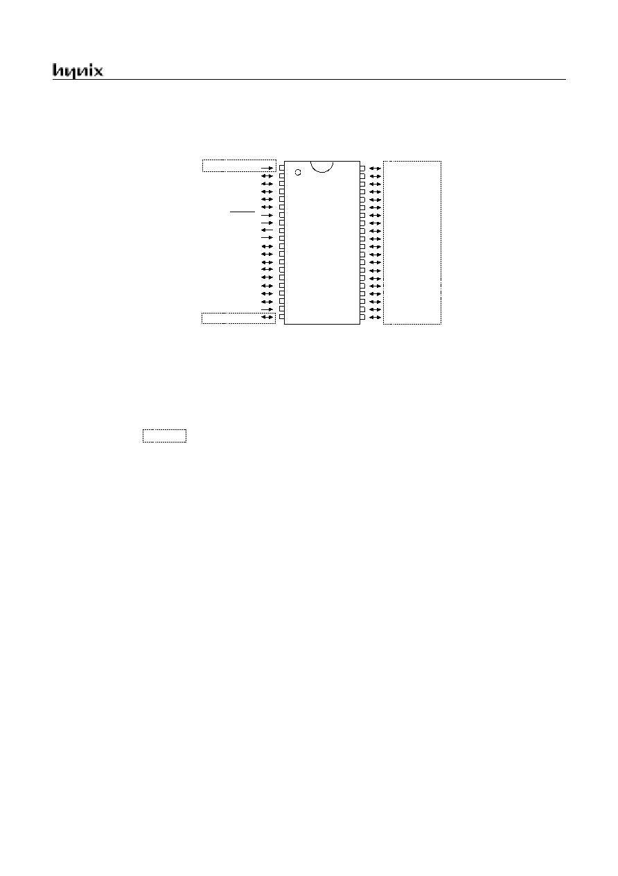
3. PIN ASSIGNMENT
High Voltage Port
R53
R54
R55
R56
R57
RESET
XI
XO
V
SS
SCLK
SIN
SOUT
PWM1O/T1O
AN0
AV
SS
R60
R61
R62
R63
R64
R65
R66
R67
AV
DD
AN1
AN2
AN3
AN4
AN5
AN6
AN7
RA
R34
R33
R32
R31
R30
R27
R26
R25
R24
R23
R22
R21
R20
R05
R04
R03
R02
R01
R00
V
DD
42SDIP
1
2
3
4
5
6
7
8
9
10
11
12
13
14
15
16
17
18
19
20
21
42
41
40
39
38
37
36
35
34
33
32
31
30
29
28
27
26
25
24
23
22
BUZO
EC0
INT1
INT0
V
disp
R07
R06
GM
S
8
1C
2
112
/20
R57
RESET
XI
XO
V
SS
AV
SS
R60
R61
R62
R63
R64
AN1
AN0
R27
R26
R25
R24
R23
R22
R21
R20
R07
R06
R05
NC
R5
5
R5
4
R5
3
RA
R3
4
R3
3
R3
2
R3
1
R3
0
R5
6
R6
5
R6
7
AV
DD
V
DD
R0
0
R0
1
R0
2
R0
3
R0
4
NC
R6
6
AN5
AN6
AN7
12
13
14
15
16
17
18
19
20
21
22
41
40
39
38
37
36
35
34
44
43
42
33
32
31
30
29
28
27
26
25
24
23
1
2
3
4
5
6
7
8
9
10
11
44MQFP
AN2
AN3
AN4
INT
0
INT
1
EC0
BUZ
O
SO
UT
SI
N
SCL
K
PWM
1
O
/
T
1
O
GMS81C2112/20
Vd
isp
GMS81C2112/GMS81C2120
JUNE. 2001 Ver 1.00
5
High Voltage Port
R53
R54
R55
R56
R57
RESET
XI
XO
V
SS
SCLK
SIN
SOUT
PWM1O/T1O
AN0
R60
R61
R62
R63
R64
R65
R66
R67
AN1
AN2
AN3
AN4
AN5
AN6
AN7
RA
R34
R33
R32
R31
R30
R27
R26
R25
R24
R23
R22
R21
R20
R05
R04
R03
R02
R01
R00
V
DD
40PDIP
1
2
3
4
5
6
7
8
9
10
11
12
13
14
15
16
17
18
19
20
40
39
38
37
36
35
34
33
32
31
30
29
28
27
26
25
24
23
22
21
BUZO
EC0
INT1
INT0
V
disp
R07
R06
G
M
S
8
1
C
21
12/
20
GMS81C2112/GMS81C2120
6
JUNE. 2001 Ver 1.00
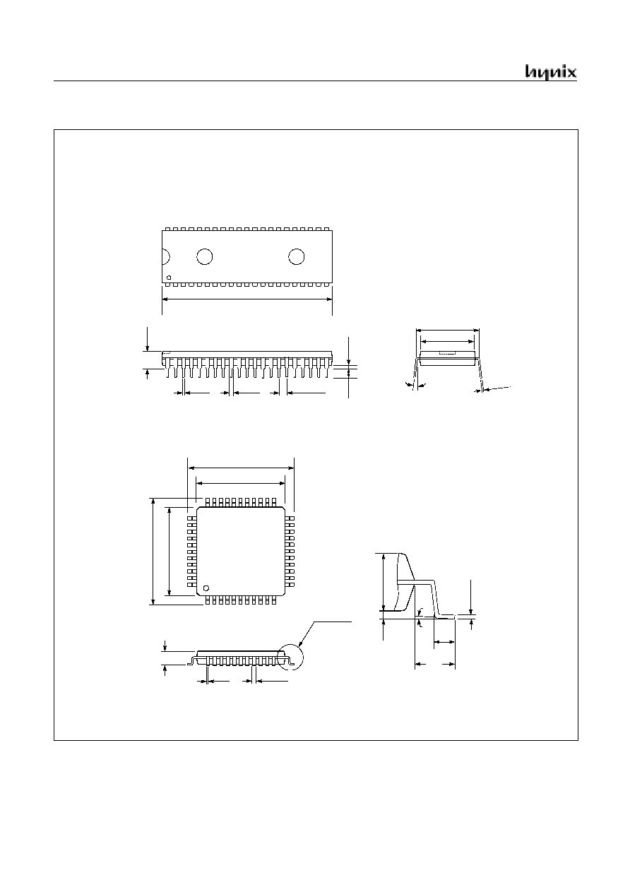
4. PACKAGE DIAGRAM
44MQFP
2.35 max.
SEE DETAIL "A"
1.03
0.73
0-7
°
0.
2
5
0.
1
0
1.60
BSC
DETAIL "A"
UNIT: MM
0.45
0.30
0.80 BSC
2.
1
0
1.
9
5
0.
2
3
0.
1
3
10.10
9.90
13.45
12.95
10
.
1
0
9.
9
0
13
.
4
5
12
.
9
5
UNIT: INCH
1.470
1.450
0.020
0.016
0.045
0.035
0.070 BSC
0.1
4
0
0.1
2
0
mi
n.
0.0
1
5
0.550
0.530
0.600 BSC
0-15
°
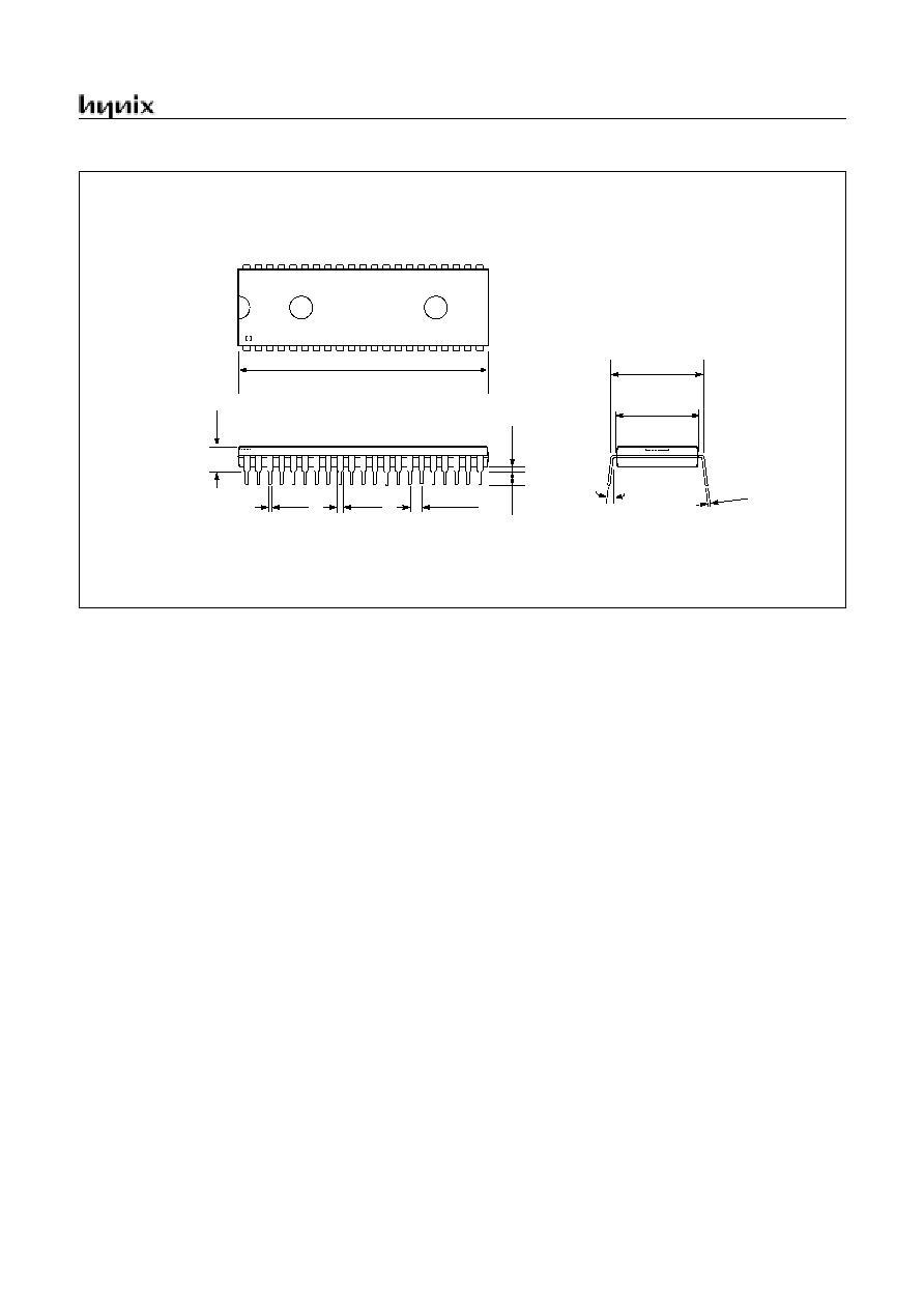
42SDIP
0.012
0.008
0
.
19
0 m
a
x.
GMS81C2112/GMS81C2120
JUNE. 2001 Ver 1.00
7
UNIT: INCH
2.075
2.045
0.022
0.015
0.100BSC
0.
1
4
0
0.
1
2
0
m
i
n. 0.0
1
5
0.550
0-15
°
40PDIP
0.012
0.008
0.
200
ma
x.
0.530
0.065
0.045
0.600 BSC

GMS81C2112/GMS81C2120
8
JUNE. 2001 Ver 1.00
5. PIN FUNCTION
V
DD
: Supply voltage.
V
SS
: Circuit ground.
AV
DD
: Supply voltage to the ladder resistor of ADC cir-
cuit. To enhance the resolution of analog to digital convert-
er, use independent power source as well as possible, other
than digital power source.
AV
SS
: ADC circuit ground.
RESET: Reset the MCU.
X
IN
: Input to the inverting oscillator amplifier and input to
the internal clock operating circuit.
X
OUT
: Output from the inverting oscillator amplifier.
RA(V
disp
): RA is one-bit high-voltage input only port pin.
In addition, RA serves the functions of the V
disp
special
features. V
disp
is used as a high-voltage input power supply
pin when selected by the mask option.
R00~R07: R0 is an 8-bit high-voltage CMOS bidirectional
I/O port. R0 pins 1 or 0 written to the Port Direction Reg-
ister can be used as outputs or inputs. In addition, R0
serves the functions of the various following special fea-
tures.
R20~R27: R2 is an 8-bit high-voltage CMOS bidirectional
I/O port. R2 pins 1 or 0 written to the Port Direction Reg-
ister can be used as outputs or inputs.
R30~R34: R3 is a 5-bit high-voltage CMOS bidirectional
I/O port. R3 pins 1 or 0 written to the Port Direction Reg-
ister can be used as outputs or inputs.
R53~R57: R5 is an 5-bit CMOS bidirectional I/O port. R5
pins 1 or 0 written to the Port Direction Register can be
used as outputs or inputs. In addition, R5 serves the func-
tions of the various following special features.
R60~R67: R6 is an 8-bit CMOS bidirectional I/O port. R6
pins 1 or 0 written to the Port Direction Register can be
used as outputs or inputs. In addition, R6 is shared with the
ADC input.
Port pin
Alternate function
RA
V
disp
(High-voltage input power supply)
Port pin
Alternate function
R00
R01
R02
R03
INT0 (External interrupt 0)
INT1 (External interrupt 1)
EC0 (Event counter input)
BUZO (Buzzer driver output)
Port pin
Alternate function
R53
R54
R55
R56
SCLK (Serial clock)
SIN (Serial data input)
SOUT (Serial data output)
PWM1O (PWM1 Output)
T1O (Timer/Counter 1 output)
Port pin
Alternate function
R60
R61
R62
R63
R64
R66
R66
R67
AN0 (Analog Input 0)
AN1 (Analog Input 1)
AN2 (Analog Input 2)
AN3 (Analog Input 3)
AN4 (Analog Input 4)
AN5 (Analog Input 5)
AN6 (Analog Input 6)
AN7 (Analog Input 7)

GMS81C2112/GMS81C2120
JUNE. 2001 Ver 1.00
9
PIN NAME
In/Out
Function
Basic
Alternate
V
DD
-
Supply voltage
V
SS
-
Circuit ground
RA (V
disp
)
I(I)
1-bit high-voltage Input only port
High-voltage input power supply pin
RESET
I
Reset signal input
XIN
I
Oscillation input
XOUT
O
Oscillation output
R00 (INT0)
I/O (I)
8-bit high-voltage I/O ports
External interrupt 0 input
R01 (INT1)
I/O (I)
External interrupt 1 input
R02 (EC0)
I/O (I)
Timer/Counter 0 external input
R03 (BUZO)
I/O (O)
Buzzer driving output
R04~R07
I/O
R20~R27
I/O
8-bit high-voltage I/O ports
R30~R34
I/O
5-bit high-voltage I/O ports
R53 (SCLK)
I/O (I/O)
5-bit high-voltage I/O ports
Serial clock source
R54 (SIN)
I/O (I)
Serial data input
R55 (SOUT)
I/O (O)
Serial data output
R56 (PWM1O/T1O)
I/O (O)
PWM 1 pulse output /Timer/Counter 1 out-
put
R57
I/O
R60~R67 (AN0~AN7)
I/O (I)
8-bit general I/O ports
Analog voltage input
AV
DD
-
Supply voltage input pin for ADC
AV
SS
-
Ground level input pin for ADC
V
DD
-
Supply voltage
V
SS
-
Circuit ground
Table 5-1 GMS81C2120 Port Function Description
GMS81C2112/GMS81C2120
10
JUNE. 2001 Ver 1.00
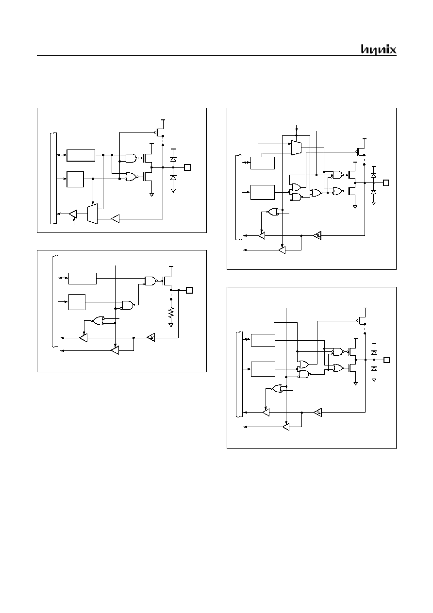
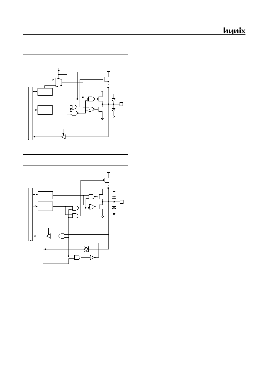
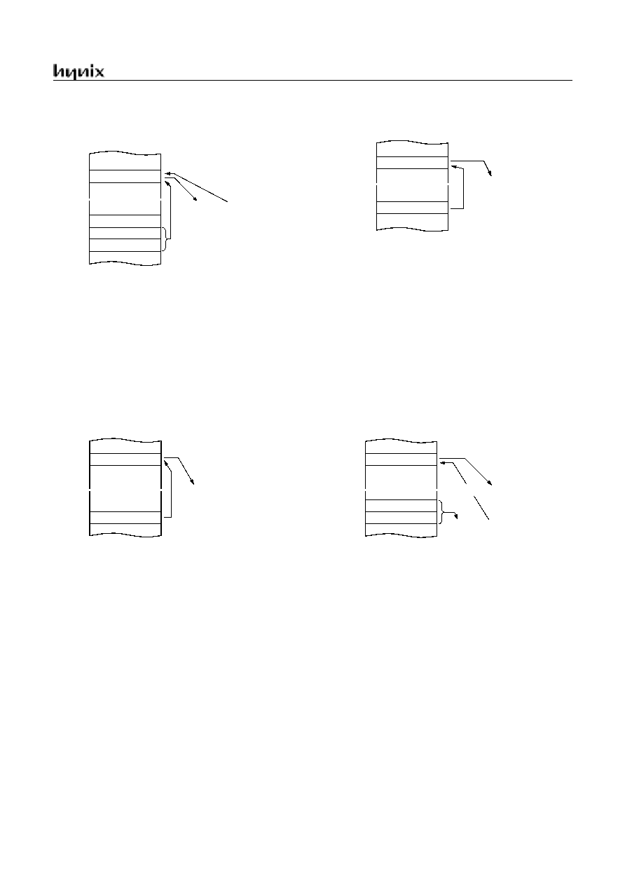
6. PORT STRUCTURES
R57
R00/INT0, R01/INT1, R02/EC0
R53/SCLK
R54/SIN
Pin
Data Reg.
Dir.
Rd
V
DD
VSS
Reg.
Da
ta
B
u
s
M UX
V
DD
Mask
Option
Pull-up
Tr.
Pin
Data Reg.
Dir.
Rd
V
DD
Vdisp
Reg.
D
a
ta
B
u
s
Selection
Data Reg.
EX) INT0
Alternate Function
Mask
Option
Data
B
u
s
V
DD
V
SS
Pin
Data Reg.
Direction
Reg.
Rd
M U X
Selection
SCLK Output
SCLK Input
V
DD
Mask
N-MOS
Open Drain Select
Option
Pull-up
Tr.
Data
B
u
s
V
DD
V
SS
Pin
Data Reg.
Direction
Reg.
Rd
Selection
SIN Input
V
DD
Mask
N-MOS
Open Drain Select
Option
Pull-up
Tr.

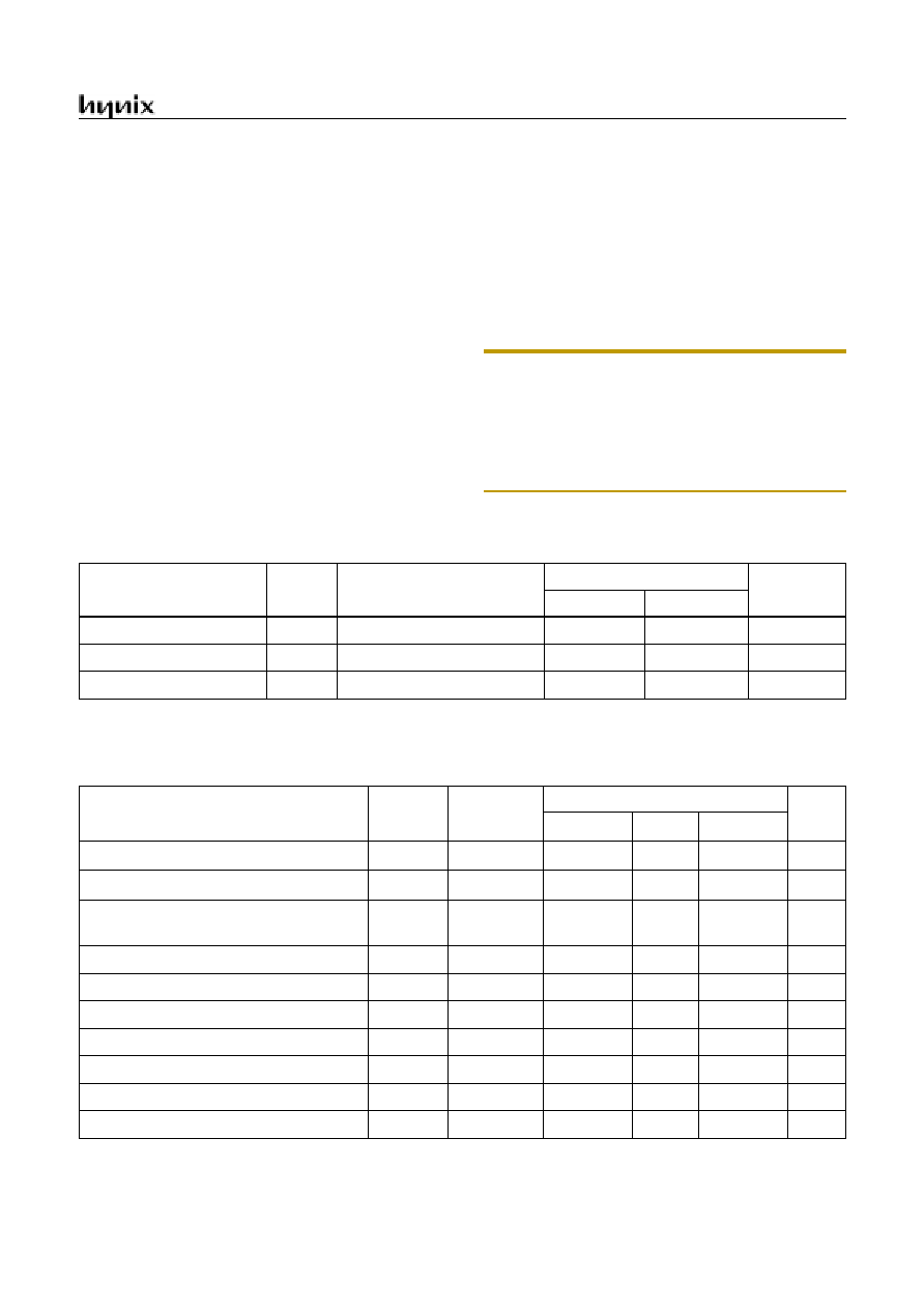
GMS81C2112/GMS81C2120
JUNE. 2001 Ver 1.00
11
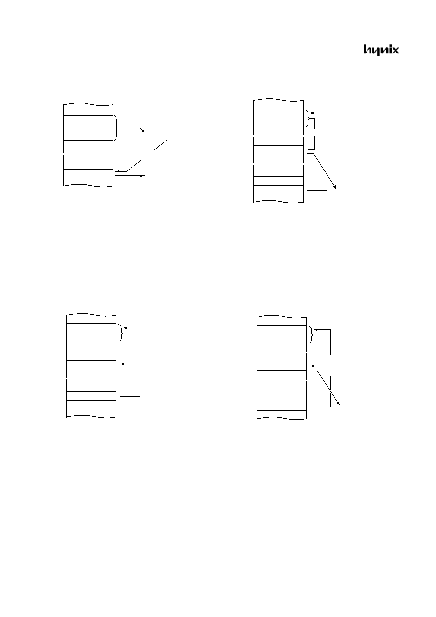
R55/SOUT
RA/Vdisp
R04~R07, R20~R27, R30~R34
RESET
XIN, XOUT
R03/BUZO
Data
B
u
s
V
DD
V
SS
Pin
Data Reg.
Direction
Reg.
Rd
M U X
Selection
SOUT output
IOSWIN Input
V
DD
Mask
N-MOS
Open Drain Select
IOSWB
Option
Pull-up
Tr.
Rd
Vdisp
Data bus
V
DD
Mask
Option
Pin
Data Reg.
Dir.
Rd
V
DD
Vdisp
Reg.
Da
ta B
u
s
MUX
Mask
Option
RESET
V
DD
V
SS
OTP :disconnected
Main :connected
XOUT
V
DD
XIN
Stop
Mainclk Off
V
SS
Pin
Data Reg.
Dir.
Rd
V
DD
Vdisp
Reg.
Da
ta B
u
s
M UX
M U X
Selection
Data Reg.
Secondary
Function
Mask
Option
GMS81C2112/GMS81C2120
12
JUNE. 2001 Ver 1.00
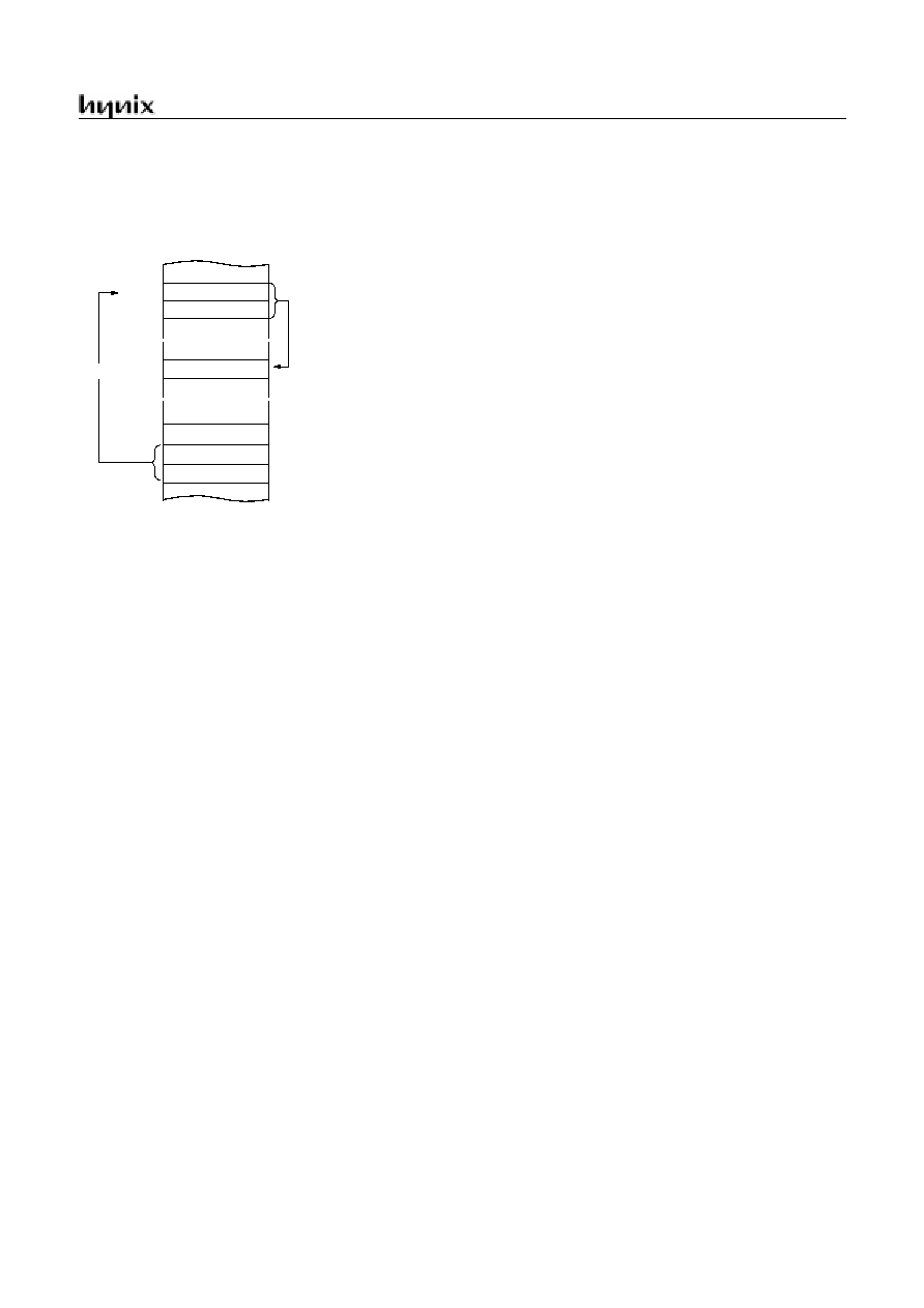
R56/PWM1O/T1O
R60~R67/AN0~AN7
Da
ta B
u
s
V
DD
V
SS
Pin
Data Reg.
Direction
Reg.
Rd
M U X
Selection
SOUT output
V
DD
Mask
N-MOS
Open Drain Select
Option
Pull-up
Tr.
Da
ta
B
u
s
V
DD
V
SS
Pin
Data Reg.
Direction
Reg.
Rd
V
DD
Mask
A/D
Analog
Converter
Input Mode
A/D Ch.
Selection
Option
Pull-up
Tr.
GMS81C2112/GMS81C2120
JUNE. 2001 Ver 1.00
13
7. ELECTRICAL CHARACTERISTICS
7.1 Absolute Maximum Ratings
Supply voltage ............................................. -0.3 to +7.0 V
Storage Temperature .................................... -40 to +85
°
C
Voltage on Normal voltage pin
with respect to Ground (V
SS
)
..............................................................-0.3 to V
DD
+0.3 V
Voltage on High voltage pin
with respect to Ground (V
SS
)
............................................................ -45V to V
DD
+0.3 V
Maximum current out of V
SS
pin .......................... 150 mA
Maximum current into V
DD
pin .............................. 80 mA
Maximum current sunk by (I
OL
per I/O Pin) .......... 20 mA
Maximum output current sourced by (I
OH
per I/O Pin)
................................................................................... 8 mA
Maximum current (
I
OL
) ...................................... 100 mA
Maximum current (
I
OH
)........................................ 50 mA
Note: Stresses above those listed under "Absolute Maxi-
mum Ratings" may cause permanent damage to the de-
vice. This is a stress rating only and functional operation of
the device at any other conditions above those indicated in
the operational sections of this specification is not implied.
Exposure to absolute maximum rating conditions for ex-
tended periods may affect device reliability.
7.2 Recommended Operating Conditions
7.3 A/D Converter Characteristics
(T
A
=25
°
C, V
DD
=5V, V
SS
=0V, AV
DD
=5.12V, AV
SS
=0V @
f
XIN
=4MHz)
Parameter
Symbol
Condition
Specifications
Unit
Min.
Max.
Supply Voltage
V
DD
f
XI
= 4.5 MHz
2.7
5.5
V
Operating Frequency
f
XIN
V
DD
= V
DD
1
4.5
MHz
Operating Temperature
T
OPR
-40
85
°
C
Parameter
Symbol
Condition
Specifications
Unit
Min.
Typ.
1
1. Data in "Typ" column is at 25
°
C unless otherwise stated. These parameters are for design guidance only and are not tested.
Max.
Analog Power Supply Input Voltage Range
AV
DD
AV
SS
-
AV
DD
V
Analog Input Voltage Range
V
AN
AV
SS
-0.3
AV
DD
+0.3
V
Current Following
Between AV
DD
and
AV
SS
I
AVDD
-
-
200
uA
Overall Accuracy
CA
IN
-
-
±
2
LSB
Non-Linearity Error
N
NLE
-
-
±
2
LSB
Differential Non-Linearity Error
N
DNLE
-
-
±
2
LSB
Zero Offset Error
N
ZOE
-
-
±
2
LSB
Full Scale Error
N
FSE
-
-
±
2
LSB
Gain Error
N
NLE
-
-
±
2
LSB
Conversion Time
T
CONV
f
XIN
=4MHz
-
-
20
us
GMS81C2112/GMS81C2120
14
JUNE. 2001 Ver 1.00
7.4
DC Electrical Characteristics for Standard Pins(5V)
(V
DD
= 5.0V ± 10%, V
SS
= 0V, T
A
= -40 ~ 85°C, f
XIN
= 4 MHz, Vdisp = V
DD
-40V to V
DD
)
,
Parameter
Pin
Symbol
Test Condition
Specification
Unit
Min
Typ.
1
1. Data in "Typ." column is at 4.5V, 25
°
C unless otherwise stated. These parameters are for design guidance only and are not tested.
Max
Input High Voltage
XIN
V
IH1
External Clock
0.9V
DD
V
DD
+0.3
V
RESET,SIN,R55,SCLK,
INT0
&
1,EC0
V
IH2
0.8V
DD
V
DD
+0.3
R53~R57,R6
V
IH3
0.7V
DD
V
DD
+0.3
Input Low Voltage
XIN
V
IL1
External Clock
-0.3
0.1V
DD
V
RESET,SIN,,R55,SCLK,
INT0
&
1,EC0
V
IL2
-0.3
0.2V
DD
R53~R57,R6
V
IL3
-0.3
0.3V
DD
Output High
Voltage
R53~R57,R6,BUZO,
PWM1O/T1O,SCLK,SOUT
V
OH
I
OH
= -0.5mA
V
DD
-0.5
V
Output Low
Voltage
R53~R57,R6,BUZO,
PWM1O/T1O,SCLK,SOUT
V
OL1
V
OL2
I
OL
= 1.6mA
I
OL
= 10mA
0.4
2
V
Input High
Leakage Current
R53~R57,R6
I
IH1
1
uA
Input Low
Leakage Current
R53~R57,R6
I
IL1
-1
uA
Input Pull-up
Current(*Option)
R53~R57,R6
I
PU
50
100
180
uA
Power Fail
Detect Voltage
V
DD
V
PFD
2.7
V
Current dissipation
in active mode
V
DD
I
DD
f
XIN
=4.5MHz
8
mA
Current dissipation
in standby mode
V
DD
I
STBY
f
XIN
=4.5MHz
3
mA
Current dissipation
in stop mode
V
DD
I
STOP
f
XIN
=Off
f
SXIN
=32.7KHz
10
uA
Hysteresis
RESET,SIN,R55,SCLK,
INT0
,
INT1,EC0
V
T+
~V
T-
0.4
V
Internal RC WDT
Frequency
XOUT
T
RCWDT
8
30
KHz
RC Oscillation
Frequency
XOUT
f
RCOSC
R= 120K
1.5
2
2.5
MHz

GMS81C2112/GMS81C2120
JUNE. 2001 Ver 1.00
15
7.5 DC Electrical Characteristics for High-Voltage Pins
(V
DD
= 5.0V ± 10%, V
SS
= 0V, T
A
= -40 ~ 85°C, f
XIN
= 4 MHz, Vdisp = V
DD
-40V to V
DD
)
Parameter
Pin
Symbol
Test Condition
Specification
Unit
Min
Typ.
1
1. Data in "Typ." column is at 4.5V, 25
°
C unless otherwise stated. These parameters are for design guidance only and are not tested.
Max
Input High Voltage
R0,R2,R30~R34,RA
V
IH
0.7V
DD
V
DD
+0.3
V
Input Low Voltage
R0,R2,R30~R34,RA
V
IL
V
DD
-40
0.3V
DD
V
Output High
Voltage
R0,R2,R30~R34
V
OH
I
OH
= -15mA
I
OH
= -10mA
I
OH
= - 4mA
V
DD
-3.0
V
DD
-2.0
V
DD
-1.0
V
Output Low
Voltage
R0,R2,R30~R34
V
OL
Vdisp = V
DD
-40
150K
atV
DD
-
40
V
DD
-37
V
DD
-37
V
Input High
Leakage Current
R0,R2,R30~R34,RA
I
IH
V
IN
=V
DD
-40V
to V
DD
20
uA
Input Pull-down
Current(*Option)
R0,R2,R30~R34
I
PD
Vdisp=V
DD
-35V
V
IN
=V
DD
200
600
1000
uA
Input High Voltage
R0,R2,R30~R34,RA
V
IH
0.7V
DD
V
DD
+0.3
V
GMS81C2112/GMS81C2120
16
JUNE. 2001 Ver 1.00
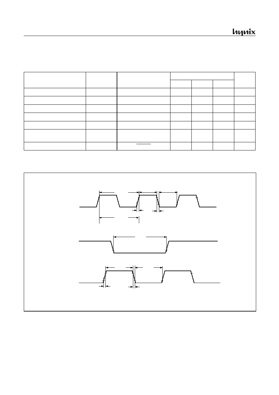
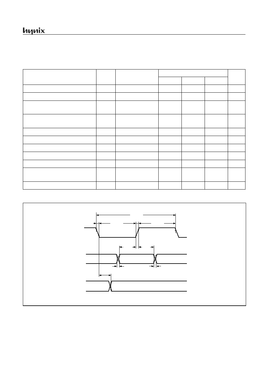
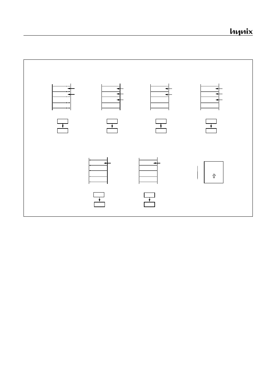
7.6 AC Characteristics
(T
A
=-40~ 85
°
C, V
DD
=5V
±
10%
,
V
SS
=0V)
Figure 7-1 Timing Chart
Parameter
Symbol
Pins
Specifications
Unit
Min.
Typ.
Max.
Operating Frequency
f
CP
XIN
1
-
8
MHz
External Clock Pulse Width
t
CPW
XIN
80
-
-
nS
External Clock Transition Time
t
RCP,
t
FCP
XIN
-
-
20
nS
Oscillation Stabilizing Time
t
ST
XIN, XOUT
-
-
20
mS
External Input Pulse Width
t
EPW
INT0, INT1, EC0
2
-
-
t
SYS
External Input Pulse Transi-
tion Time
t
REP,
t
FEP
INT0, INT1, EC0
-
-
20
nS
RESET Input Width
t
RST
RESET
8
-
-
t
SYS
t
RCP
t
FCP
XI
INT0, INT1
0.5V
V
DD
-0.5V
0.2V
DD
RESETB
t
REP
t
FEP
0.2V
DD
0.8V
DD
EC0
t
RST
t
EPW
t
EPW
1/f
CP
t
CPW
t
CPW
t
SYS
GMS81C2112/GMS81C2120
JUNE. 2001 Ver 1.00
17
7.7 AC Characteristics
(T
A
=-40~+85
°
C, V
DD
=5V
±
10%, V
SS
=0V, f
XIN
=4MHz)
Figure 7-2 Serial I/O Timing Chart
Parameter
Symbol
Pins
Specifications
Unit
Min.
Typ.
Max.
Serial Input Clock Pulse
t
SCYC
SCLK
2t
SYS
+200
-
8
ns
Serial Input Clock Pulse Width
t
SCKW
SCLK
t
SYS
+70
-
8
ns
Serial Input Clock Pulse Transition
Time
t
FSCK
t
RSCK
SCLK
-
-
30
ns
SIN Input Pulse Transition Time
t
FSIN
t
RSIN
SIN
-
-
30
ns
SIN Input Setup Time (External SCLK)
t
SUS
SIN
100
-
-
ns
SIN Input Setup Time (Internal SCLK)
t
SUS
SIN
200
-
ns
SIN Input Hold Time
t
HS
SIN
t
SYS
+70
-
ns
Serial Output Clock Cycle Time
t
SCYC
SCLK
4t
SYS
-
16t
SYS
ns
Serial Output Clock Pulse Width
t
SCKW
SCLK
t
SYS
-30
ns
Serial Output Clock Pulse Transition
Time
t
FSCK
t
RSCK
SCLK
30
ns
Serial Output Delay Time
s
OUT
SOUT
100
ns
SCLK
SIN
0.2V
DD
SOUT
0.2V
DD
0.8V
DD
t
SCYC
t
SCKW
t
SCKW
t
RSCK
t
FSCK
0.8V
DD
t
SUS
t
HS
t
DS
0.2V
DD
0.8V
DD
t
RSIN
t
FSIN
GMS81C2112/GMS81C2120
18
JUNE. 2001 Ver 1.00
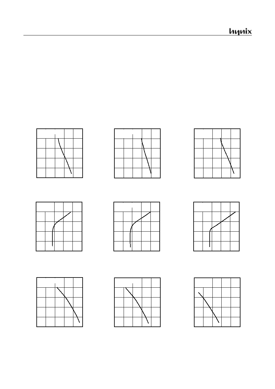
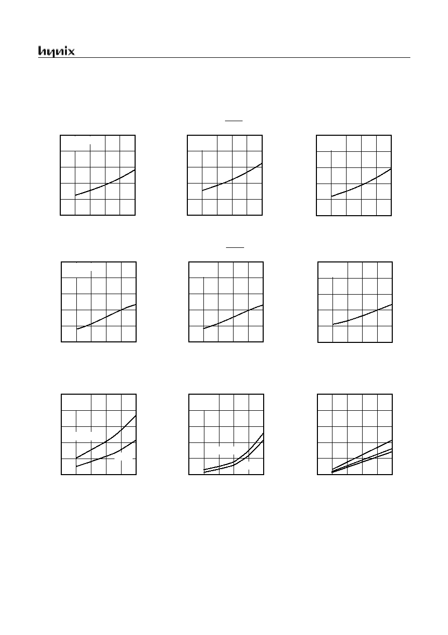
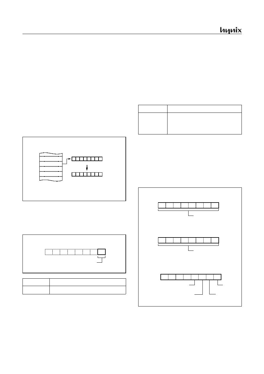
7.8 Typical Characteristics
This graphs and tables provided in this section are for de-
sign guidance only and are not tested or guaranteed.
In some graphs or tables the data presented are out-
side specified operating range (e.g. outside specified
V
DD
range). This is for information only and devices
are guaranteed to operate properly only within the
specified range.
The data presented in this section is a statistical summary
of data collected on units from different lots over a period
of time. "Typical" represents the mean of the distribution
while "max" or "min" represents (mean + 3
) and (mean
-
3
) respectively where
is standard deviation
I
OH
-
V
OH
-1.6
-1.2
-0.8
-0.4
0
4.6
4.7
4.8
4.9
5.0 (V)
Ta=25
°
C
V
DD
=5.0V
(mA)
I
OH
V
OH
I
OH
-
V
OH
-1.6
-1.2
-0.8
-0.4
0
3.6
3.7
3.8
3.9
4.0 (V)
Ta=25
°
C
V
DD
=4.0V
(mA)
I
OH
V
OH
I
OH
-
V
OH
-1.6
-1.2
-0.8
-0.4
0
2.6
2.7
2.8
2.9
3.0 (V)
Ta=25
°
C
V
DD
=3.0V
(mA)
I
OH
V
OH
I
OL
-
V
OL
16
12
8
4
0
0.6
0.8
1.0
1.2
1.4 (V)
Ta=25
°
C
V
DD
=5.0V
(mA)
I
OL
V
OL
I
OL
-
V
OL
16
12
8
4
0
0.6
0.8
1.0
1.2
1.4 (V)
Ta=25
°
C
V
DD
=4.0V
(mA)
I
OL
V
OL
I
OL
-
V
OL
16
12
8
4
0
0.6
0.8
1.0
1.2
1.4 (V)
Ta=25
°
C
V
DD
=3.0V
(mA)
I
OL
V
OL
I
OH
-
V
OH
-16
-12
-8
-4
0
1.0
2.0
3.0
4.0
5.0 (V)
Ta=25
°
C
V
DD
=5.0V
(mA)
I
OH
V
OH
I
OH
-
V
OH
-16
-12
-8
-4
0
1.0
2.0
3.0
4.0
5.0 (V)
Ta=25
°
C
V
DD
=4.0V
(mA)
I
OH
V
OH
I
OH
-
V
OH
-16
-12
-8
-4
0
1.0
2.0
3.0
4.0
5.0 (V)
Ta=25
°
C
V
DD
=3.0V
(mA)
I
OH
V
OH
R40~R43, R6, R53~R57
BUZO, PWM1O/T1O
SCLK, SOUT pins
R0, R2,RA
R30~R34 pins
R40~R43, R6, R53~R57
BUZO, PWM1O/T1O
SCLK, SOUT pins
GMS81C2112/GMS81C2120
JUNE. 2001 Ver 1.00
19
Ta=25
°
C
I
DD
-
V
DD
4.0
3.0
2.0
1.0
0
(mA)
I
DD
2
3
4
5
6
V
DD
(V)
Normal Operation
I
STOP
-
V
DD
2.0
1.5
1.0
0.5
0
(
µ
A)
I
DD
2
3
4
5
6
V
DD
(V)
Stop Mode
85
°
C
25
°
C
-20
°
C
f
XIN
= 4.5MHz
2.5MHz
Ta=25
°
C
I
SBY
-
V
DD
4.0
3.0
2.0
1.0
0
(mA)
I
DD
2
3
4
5
6
V
DD
(V)
Stand-by Mode
f
XIN
= 4.5MHz
2.5MHz
V
DD
-
V
IL2
4
3
2
1
0
(V)
V
IL2
2
3
4
5
6
V
DD
(V)
V
DD
-
V
IL1
4
3
2
1
0
(V)
V
IL1
2
3
4
5
6
V
DD
(V)
Ta=25
°
C
1
f
XIN
=4.5MHz
Ta=25
°
C
f
XIN
=4.5MHz
V
DD
-
V
IL3
4
3
2
1
0
(V)
V
IL3
2
3
4
5
6
V
DD
(V)
Ta=25
°
C
1
f
XIN
=4.5MHz
RESET, R55, SIN, SCLK
INT0, INT1, EC0 pins
XIN pins
V
DD
-
V
IH2
4
3
2
1
0
(V)
V
IH2
2
3
4
5
6
V
DD
(V)
V
DD
-
V
IH1
4
3
2
1
0
(V)
V
IH1
2
3
4
5
6
V
DD
(V)
Ta=25
°
C
1
f
XIN
=4.5MHz
Ta=25
°
C
f
XIN
=4.5MHz
V
DD
-
V
IH3
4
3
2
1
0
(V)
V
IH3
2
3
4
5
6
V
DD
(V)
Ta=25
°
C
1
f
XIN
=4.5MHz
RESET, R55, SIN, SCLK
INT0, INT1, EC0 pins
XIN pins
R53~R57, R6 pins
R53~R57, R6 pins
GMS81C2112/GMS81C2120
20
JUNE. 2001 Ver 1.00
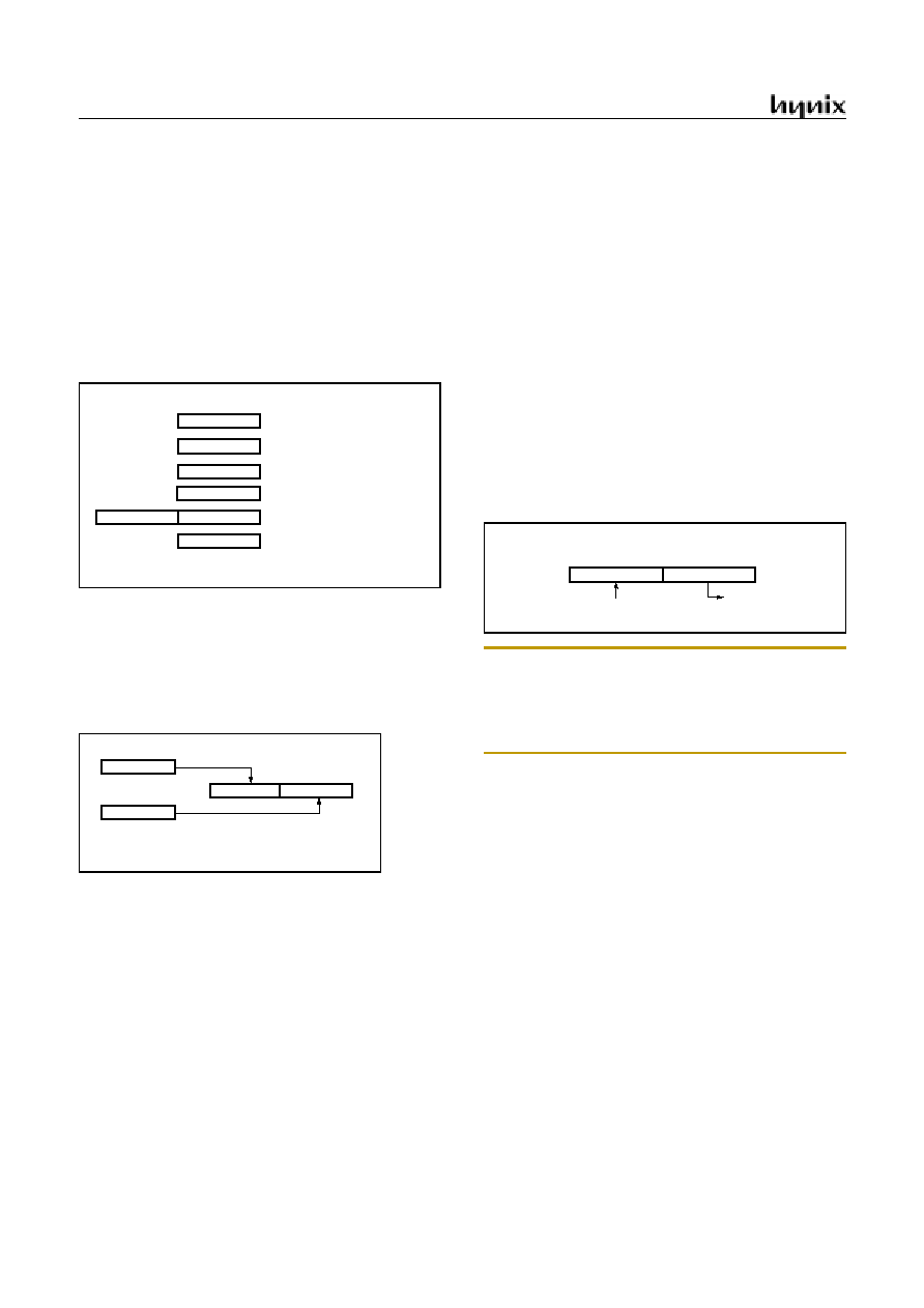
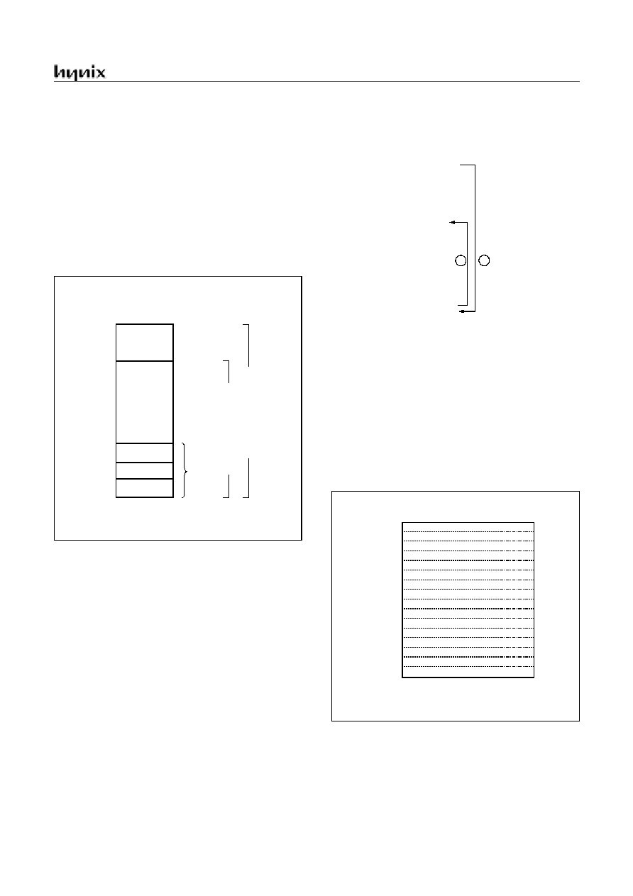
8. MEMORY ORGANIZATION
The GMS81C2112 and GMS81C2120 have separate ad-
dress spaces for Program memory and Data Memory. Pro-
gram memory can only be read, not written to. It can be up
to 12K/20K bytes of Program memory. Data memory can
be read and written to up to 448 bytes including the stack
area.
8.1 Registers
This device has six registers that are the Program Counter
(PC), a Accumulator (A), two index registers (X, Y), the
Stack Pointer (SP), and the Program Status Word (PSW).
The Program Counter consists of 16-bit register.
Figure 8-1 Configuration of Registers
Accumulator: The Accumulator is the 8-bit general pur-
pose register, used for data operation such as transfer, tem-
porary saving, and conditional judgement, etc.
The Accumulator can be used as a 16-bit register with Y
Register as shown below.
Figure 8-2 Configuration of YA 16-bit Register
X, Y Registers: In the addressing mode which uses these
index registers, the register contents are added to the spec-
ified address, which becomes the actual address. These
modes are extremely effective for referencing subroutine
tables and memory tables. The index registers also have in-
crement, decrement, comparison and data transfer func-
tions, and they can be used as simple accumulators.
Stack Pointer: The Stack Pointer is an 8-bit register used
for occurrence interrupts and calling out subroutines. Stack
Pointer identifies the location in the stack to be access
(save or restore).
Generally, SP is automatically updated when a subroutine
call is executed or an interrupt is accepted. However, if it
is used in excess of the stack area permitted by the data
memory allocating configuration, the user-processed data
may be lost.
The stack can be located at any position within 100
H
to
1FF
H
of the internal data memory. The SP is not initialized
by hardware, requiring to write the initial value (the loca-
tion with which the use of the stack starts) by using the ini-
tialization routine. Normally, the initial value of "FF
H
" is
used.
Note: The Stack Pointer must be initialized by software be-
cause its value is undefined after RESET.
Example: To initialize the SP
LDX
#0FFH
TXSP
; SP
FF
H
Program Counter: The Program Counter is a 16-bit wide
which consists of two 8-bit registers, PCH and PCL. This
counter indicates the address of the next instruction to be
executed. In reset state, the program counter has reset rou-
tine address (PC
H
:0FF
H
, PC
L
:0FE
H
).
Program Status Word: The Program Status Word (PSW)
contains several bits that reflect the current state of the
CPU. The PSW is described in Figure 8-3. It contains the
Negative flag, the Overflow flag, the Break flag the Half
Carry (for BCD operation), the Interrupt enable flag, the
Zero flag, and the Carry flag.
[Carry flag C]
This flag stores any carry or borrow from the ALU of CPU
after an arithmetic operation and is also changed by the
Shift Instruction or Rotate Instruction.
[Zero flag Z]
This flag is set when the result of an arithmetic operation
or data transfer is "0" and is cleared by any other result.
ACCUMULATOR
X REGISTER
Y REGISTER
STACK POINTER
PROGRAM COUNTER
PROGRAM STATUS
WORD
X
A
SP
Y
PCL
PSW
PCH
Two 8-bit Registers can be used as a "YA" 16-bit Register
Y
A
Y
A
SP
01
H
Stack Address ( 100
H
~ 1FE
H
)
Bit 15
Bit 0
8 7
Hardware fixed
00
H
~FF
H
GMS81C2112/GMS81C2120
JUNE. 2001 Ver 1.00
21
Figure 8-3 PSW (Program Status Word) Register
[Interrupt disable flag I]
This flag enables/disables all interrupts except interrupt
caused by Reset or software BRK instruction. All inter-
rupts are disabled when cleared to "0". This flag immedi-
ately becomes "0" when an interrupt is served. It is set by
the EI instruction and cleared by the DI instruction.
[Half carry flag H]
After operation, this is set when there is a carry from bit 3
of ALU or there is no borrow from bit 4 of ALU. This bit
can not be set or cleared except CLRV instruction with
Overflow flag (V).
[Break flag B]
This flag is set by software BRK instruction to distinguish
BRK from TCALL instruction with the same vector ad-
dress.
[Direct page flag G]
This flag assigns RAM page for direct addressing mode. In
the direct addressing mode, addressing area is from zero
page 00
H
to 0FF
H
when this flag is "0". If it is set to "1",
addressing area is assigned 100
H
to 1FF
H
. It is set by
SETG instruction and cleared by CLRG.
[Overflow flag V]
This flag is set to "1" when an overflow occurs as the result
of an arithmetic operation involving signs. An overflow
occurs when the result of an addition or subtraction ex-
ceeds +127(7F
H
) or -128(80
H
). The CLRV instruction
clears the overflow flag. There is no set instruction. When
the BIT instruction is executed, bit 6 of memory is copied
to this flag.
[Negative flag N]
This flag is set to match the sign bit (bit 7) status of the re-
sult of a data or arithmetic operation. When the BIT in-
struction is executed, bit 7 of memory is copied to this flag.
N
NEGATIVE FLAG
V
G
B
H
I
Z
C
MSB
LSB
RESET VALUE : 00
H
PSW
OVERFLOW FLAG
BRK FLAG
CARRY FLAG RECEIVES
ZERO FLAG
INTERRUPT ENABLE FLAG
CARRY OUT
HALF CARRY FLAG RECEIVES
CARRY OUT FROM BIT 1 OF
ADDITION OPERLANDS
SELECT DIRECT PAGE
when G=1, page is selected to "page 1"
GMS81C2112/GMS81C2120
22
JUNE. 2001 Ver 1.00
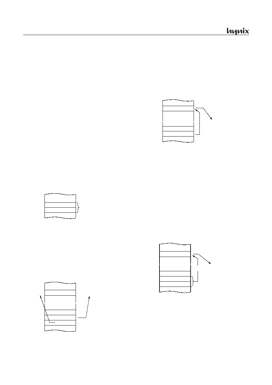
Figure 8-4 Stack Operation
At execution of
a CALL/TCALL/PCALL
PCL
PCH
01FB
SP after
execution
SP before
execution
01FC
01FC
01FD
01FE
01FE
Push
down
At acceptance
of interrupt
PCL
PCH
01FB
01FB
01FC
01FD
01FE
01FE
Push
down
PSW
At execution
of RET instruction
PCL
PCH
01FB
01FE
01FC
01FD
01FE
01FC
Pop
up
At execution
of RET instruction
PCL
PCH
01FB
01FE
01FC
01FD
01FE
01FB
Pop
up
PSW
0100H
01FEH
Stack
depth
At execution
of PUSH instruction
A
01FB
01FD
01FC
01FD
01FE
01FE
Push
down
SP after
execution
SP before
execution
PUSH A (X,Y,PSW)
At execution
of POP instruction
A
01FB
01FE
01FC
01FD
01FE
01FD
Pop
up
POP A (X,Y,PSW)
GMS81C2112/GMS81C2120
JUNE. 2001 Ver 1.00
23
8.2 Program Memory
A 16-bit program counter is capable of addressing up to
64K bytes, but this device has 20K bytes program memory
space only physically implemented. Accessing a location
above FFFF
H
will cause a wrap-around to 0000
H
.
Figure 8-5, shows a map of Program Memory. After reset,
the CPU begins execution from reset vector which is stored
in address FFFE
H
and FFFF
H
as shown in Figure 8-6.
As shown in Figure 8-5, each area is assigned a fixed loca-
tion in Program Memory. Program Memory area contains
the user program.
Figure 8-5 Program Memory Map
Page Call (PCALL) area contains subroutine program to
reduce program byte length by using 2 bytes PCALL in-
stead of 3 bytes CALL instruction. If it is frequently called,
it is more useful to save program byte length.
Table Call (TCALL) causes the CPU to jump to each
TCALL address, where it commences the execution of the
service routine. The Table Call service area spaces 2-byte
for every TCALL: 0FFC0
H
for TCALL15, 0FFC2
H
for
TCALL14, etc., as shown in Figure 8-7.
Example: Usage of TCALL
The interrupt causes the CPU to jump to specific location,
where it commences the execution of the service routine.
The External interrupt 0, for example, is assigned to loca-
tion 0FFFA
H
. The interrupt service locations spaces 2-byte
interval: 0FFF8
H
and 0FFF9
H
for External Interrupt 1,
0FFFA
H
and 0FFFB
H
for External Interrupt 0, etc.
Any area from 0FF00
H
to 0FFFF
H
, if it is not going to be
used, its service location is available as general purpose
Program Memory.
Figure 8-6 Interrupt Vector Area
Interrupt
Vector Area
D000
H
FEFF
H
FF00
H
FFC0
H
FFDF
H
FFE0
H
FFFF
H
PCAL
L
a
r
e
a
B000
H
TCALL area
GM
S
8
1C
2
112
, 1
2
K
R
O
M
GMS
8
1C
2
120
, 20
K
R
O
M
LDA
#5
TCALL
0FH
;
1BYTE INSTR UCTIO N
:
;
INSTEAD O F 3 BYTES
:
;
NO R M AL C ALL
;
;TABLE CALL ROUTINE
;
FUNC_A:
LDA
LRG0
RET
;
FUNC_B:
LDA
LRG1
RET
;
;TABLE CALL ADD. AREA
;
ORG
0FFC0H
;
TCALL ADDRESS AREA
DW
FUNC_A
DW
FUNC_B
1
2
0FFE0H
E2
Address
Vector Area Memory
E4
E6
E8
EA
EC
EE
F0
F2
F4
F6
F8
FA
FC
FE
-
-
Serial Communication Interface
Basic Interval Timer
-
-
-
Timer/Counter 0 Interrupt
-
External Interrupt 0
-
RESET Vector Area
External Interrupt 1
Watchdog Timer Interrupt
"-" means reserved area.
NOTE:
Timer/Counter 1 Interrupt
-
A/D Converter
GMS81C2112/GMS81C2120
24
JUNE. 2001 Ver 1.00
Figure 8-7 PCALL and TCALL Memory Area
PCALL
rel
4F35
PCALL 35H
TCALL
n
4A
TCALL
4
0FFC0
H
C1
Address
Program Memory
C2
C3
C4
C5
C6
C7
C8
0FF00
H
Address
PCALL Area Memory
0FFFF
H
PCALL Area
(256 Bytes)
* means that the BRK software interrupt is using
same address with TCALL0.
NOTE:
TCALL 15
TCALL 14
TCALL 13
TCALL 12
TCALL 11
TCALL 10
TCALL 9
TCALL 8
TCALL 7
TCALL 6
TCALL 5
TCALL 4
TCALL 3
TCALL 2
TCALL 1
TCALL 0 / BRK *
C9
CA
CB
CC
CD
CE
CF
D0
D1
D2
D3
D4
D5
D6
D7
D8
D9
DA
DB
DC
DD
DE
DF
4F
~
~
~
~
NEXT
35
0FF35
H
0FF00
H
0FFFF
H
11111111 11010110
01001010
PC:
FH
FH
DH 6H
4A
~
~
~
~
25
0FFD6
H
0FF00
H
0FFFF
H
D1
NEXT
0FFD7
H
0D125
H
Reverse

GMS81C2112/GMS81C2120
JUNE. 2001 Ver 1.00
25
Example: The usage software example of Vector address for GMS81C2120.
ORG
0FFE0H
DW
NOT_USED
DW
NOT_USED
DW
SIO
; Serial Interface
DW
BIT_TIMER
; Basic Interval Timer
DW
WD_TIMER
; Watchdog Timer
DW
ADC
; ADC
DW
NOT_USED
DW
NOT_USED
DW
NOT_USED
DW
NOT_USED
DW
TIMER1
; Timer-1
DW
TIMER0
; Timer-0
DW
INT1
; Int.1
DW
INT0
; Int.0
DW
NOT_USED
; -
DW
RESET
; Reset
ORG
0B000H
; GMS81C2120(20K)ROM Start address
;
ORG
0D000H
; GMS81C2112(12K)ROM Start address
;*******************************************
;
MAIN PROGRAM
*
;*******************************************
;
RESET:
DI
;Disable All Interrupts
CLRG
LDX
#0
RAM_CLR: LDA
#0
;RAM Clear(!0000H->!00BFH)
STA
{X}+
CMPX
#0C0H
BNE
RAM_CLR
;
LDX
#0FFH
;Stack Pointer Initialize
TXSP
;
LDM
R0, #0
;Normal Port 0
LDM
R0IO,#82H
;Normal Port Direction
:
:
:
LDM
TDR0,#125
;8us x 125 = 1mS
LDM
TM0,#0FH
;Start Timer0, 8us at 4MHz
LDM
IRQH,#0
LDM
IRQL,#0
LDM
IENH,#0E0H
;Enable Timer0, INT0, INT1
LDM
IENL,#0
LDM
IEDS,#05H
;Select falling edge detect on INT pin
LDM
R0FUNC,#03H ;Set external interrupt pin(INT0, INT1)
EI
;Enable master interrupt
:
:
:
:
:
NOT_USED :NOP
RETI
GMS81C2112/GMS81C2120
26
JUNE. 2001 Ver 1.00
8.3 Data Memory
Figure 8-8 shows the internal Data Memory space availa-
ble. Data Memory is divided into two groups, a user RAM
(including Stack) and control registers.
Figure 8-8 Data Memory Map
User Memory
The GMS81C21xx have 448
×
8 bits for the user memory
(RAM).
Control Registers
The control registers are used by the CPU and Peripheral
function blocks for controlling the desired operation of the
device. Therefore these registers contain control and status
bits for the interrupt system, the timer/ counters, analog to
digital converters and I/O ports. The control registers are in
address range of 0C0
H
to 0FF
H
.
Note that unoccupied addresses may not be implemented
on the chip. Read accesses to these addresses will in gen-
eral return random data, and write accesses will have an in-
determinate effect.
More detailed informations of each register are explained
in each peripheral section.
Note: Write only registers can not be accessed by bit ma-
nipulation instruction. Do not use read-modify-write instruc-
tion. Use byte manipulation instruction, for example "LDM".
Example; To write at CKCTLR
LDM
CLCTLR,#09H
;Divide ratio(
÷16
)
Stack Area
The stack provides the area where the return address is
saved before a jump is performed during the processing
routine at the execution of a subroutine call instruction or
the acceptance of an interrupt.
When returning from the processing routine, executing the
subroutine return instruction [RET] restores the contents of
the program counter from the stack; executing the interrupt
return instruction [RETI] restores the contents of the pro-
gram counter and flags.
The save/restore locations in the stack are determined by
the stack pointed (SP). The SP is automatically decreased
after the saving, and increased before the restoring. This
means the value of the SP indicates the stack location
number for the next save. Refer to Figure 8-4 on page 22.
User Memory
Control
Registers
or Stack Area
0000
H
00BF
H
00C0
H
00FF
H
0100
H
01FF
H
PAGE0
User Memory
PAGE1
When "G-flag=0",
When "G-flag=1"
this page is selected
GMS81C2112/GMS81C2120
JUNE. 2001 Ver 1.00
27
Note: Several names are given at same address. Refer to
below table.
Address
Symbol
R/W
RESET
Value
Addressing
mode
0C0H
0C1H
0C4H
0C5H
0C6H
0C7H
0CAH
0CBH
0CCH
0CDH
R0
R0IO
R2
R2IO
R3
R3IO
R5
R5IO
R6
R6IO
R/W
W
R/W
W
R/W
W
R/W
W
R/W
W
Undefined
0000_0000
Undefined
0000_0000
Undefined
---0_0000
Undefined
0000_0---
Undefined
0000_0000
byte, bit
1
byte
2
byte, bit
byte
byte, bit
byte
byte, bit
byte
byte, bit
byte
0D0H
0D1H
0D1H
0D1H
0D2H
0D3H
0D3H
0D4H
0D4H
0D4H
0D5H
0DEH
TM0
T0
TDR0
CDR0
TM1
TDR1
T1PPR
T1
CDR1
T1PDR
PWM1HR
BUR
R/W
R
W
R
R/W
W
W
R
R
R/W
W
W
--00_0000
0000_0000
1111_1111
0000_0000
0000_0000
1111_1111
1111_1111
0000_0000
0000_0000
0000_0000
----_0000
1111_1111
byte, bit
byte
byte
byte
byte, bit
byte
byte
byte
byte
byte, bit
byte
byte
0E0H
0E1H
0E2H
0E3H
0E4H
0E5H
0E6H
0EAH
0EBH
0ECH
0ECH
0EDH
0EDH
0EFH
SIOM
SIOR
IENH
IENL
IRQH
IRQL
IEDS
ADCM
ADCR
BITR
CKCTLR
WDTR
WDTR
PFDR
R/W
R/W
R/W
R/W
R/W
R/W
R/W
R/W
R
R
W
R
W
R/W
0000_0001
Undefined
0000_----
0000_----
0000_----
0000_----
----_0000
-000_0001
Undefined
0000_0000
-001_0111
0000_0000
0111_1111
----_-100
byte, bit
byte, bit
byte, bit
byte, bit
byte, bit
byte, bit
byte, bit
byte, bit
byte
byte
byte
byte
byte
byte, bit
0F4H
0F6H
0F7H
0F9H
0FAH
0FBH
R0FUNC
R5FUNC
R6FUNC
R5NODR
SCMR
RA
W
W
W
W
R/W
R
----_0000
-0--_----
0000_0000
0000_0---
---0_0000
Undefined
byte
byte
byte
byte
byte
-
3
Table 8-1 Control Registers
1. "byte, bit" means that register can be addressed by not only bit
but byte manipulation instruction.
2. "byte" means that register can be addressed by only byte
manipulation instruction. On the other hand, do not use any
read-modify-write instruction such as bit manipulation for
clearing bit.
3. RA is one-bit high-voltage input only port pin. In addition, RA
serves the functions of the Vdisp special features. Vdisp is
used as a high-voltage input power supply pin when selected
by the mask option.
Addr.
When read
When write
Timer
Mode
Capture
Mode
PWM
Mode
Timer
Mode
PWM
Mode
D1H
T0
CDR0
-
TDR0
-
D3H
-
TDR1
T1PPR
D4H
T1
CDR1
T1PDR
-
T1PDR
ECH
BITR
CKCTLR
Table 8-2 Various Register Name in Same Address
GMS81C2112/GMS81C2120
28
JUNE. 2001 Ver 1.00
Address
Name
Bit 7
Bit 6
Bit 5
Bit 4
Bit 3
Bit 2
Bit 1
Bit 0
C0H
R0
R0 Port Data Register (Bit[7:0])
C1H
R0IO
R0 Port Direction Register (Bit[7:0])
C4H
R2
R2 Port Data Register (Bit[7:0])
C5H
R2IO
R2 Port Direction Register (Bit[7:0])
C6H
R3
R3 Port Data Register (Bit[4:0])
C7H
R3IO
R3 Port Direction Register (Bit[4:0])
CAH
R5
R5 Port Data Register (Bit[7:3])
CBH
R5IO
R5 Port Direction Register (Bit[7:3])
CCH
R6
R6 Port Data Register (Bit[7:0])
CDH
R6IO
R6 Port Direction Register (Bit[7:0])
D0H
TM0
-
-
CAP0
T0CK2
T0CK1
T0CK0
T0CN
T0ST
D1H
T0/TDR0/
CDR0
Timer0 Register / Timer0 Data Register / Capture0 Data Register
D2H
TM1
POL
16BIT
PWM1E
CAP1
T1CK1
T1CK0
T1CN
T1ST
D3H
TDR1/
T1PPR
Timer1 Data Register / PWM1 Period Register
D4H
T1/CDR1/
T1PDR
Timer1 Register / Capture1 Data Register / PWM1 Duty Register
D5H
PWM1HR
PWM1 High Register(Bit[3:0])
DEH
BUR
BUCK1
BUCK0
BUR5
BUR4
BUR3
BUR2
BUR1
BUR0
E0H
SIOM
POL
IOSW
SM1
SM0
SCK1
SCK0
SIOST
SIOSF
E1H
SIOR
SPI DATA REGISTER
E2H
IENH
INT0E
INT1E
T0E
T1E
E3H
IENL
ADE
WDTE
BITE
SPIE
-
-
-
-
E4H
IRQH
INT0IF
INT1IF
T0IF
T1IF
E5H
IRQL
ADIF
WDTIF
BITIF
SPIIF
-
-
-
-
E6H
IEDS
IED1H
IED1L
IED0H
IED0L
EAH
ADCM
-
ADEN
ADS3
ADS2
ADS1
ADS0
ADST
ADSF
EBH
ADCR
ADC Result Data Register
ECH
BITR
1
Basic Interval Timer Data Register
ECH
CKCTLR
1
-
WAKEUP
RCWDT
WDTON
BTCL
BTS2
BTS1
BTS0
EDH
WDTR
WDTCL
7-bit Watchdog Counter Register
EFH
PFDR
2
-
-
-
-
-
PFDIS
PFDM
PFDS
F4H
R0FUNC
-
-
-
-
BUZO
EC0
INT1
INT0
Table 8-3 Control Registers of GMS81C2120
These registers of shaded area can not be access by bit manipulation instruction as " SET1, CLR1 ", but should be access by reg-
ister operation instruction as " LDM dp,#imm ".

GMS81C2112/GMS81C2120
JUNE. 2001 Ver 1.00
29
F6H
R5FUNC
-
PWM1O/
T1O
-
-
-
-
-
-
F7H
R6FUNC
AN7
AN6
AN5
AN4
AN3
AN2
AN1
AN0
F9H
R5NODR
NODR7
NODR6
NODR5
NODR4
NODR3
-
-
-
FAH
SCMR
-
-
-
CS1
CS0
-
-
MAINOFF
FBH
RA
-
-
-
-
-
-
-
RA0
1.The register BITR and CKCTLR are located at same address. Address ECH is read as BITR, written to CKCTLR.
2.The register PFDR only be implemented on devices, not on In-circuit Emulator.
Address
Name
Bit 7
Bit 6
Bit 5
Bit 4
Bit 3
Bit 2
Bit 1
Bit 0
Table 8-3 Control Registers of GMS81C2120
These registers of shaded area can not be access by bit manipulation instruction as " SET1, CLR1 ", but should be access by reg-
ister operation instruction as " LDM dp,#imm ".
GMS81C2112/GMS81C2120
30
JUNE. 2001 Ver 1.00
8.4 Addressing Mode
The GMS800 series MCU uses six addressing modes;
· Register addressing
· Immediate addressing
· Direct page addressing
· Absolute addressing
· Indexed addressing
· Register-indirect addressing
(1) Register Addressing
Register addressing accesses the A, X, Y, C and PSW.
(2) Immediate Addressing
#imm
In this mode, second byte (operand) is accessed as a data
immediately.
Example:
0435
ADC
#35H
When G-flag is 1, then RAM address is defined by 16-bit
address which is composed of 8-bit RAM paging register
(RPR) and 8-bit immediate data.
Example: G=1
E45535
LDM
35H,#55H
(3) Direct Page Addressing
dp
In this mode, a address is specified within direct page.
Example; G=0
C535
LDA
35H
;A
RAM[35H]
(4) Absolute Addressing
!abs
Absolute addressing sets corresponding memory data to
Data, i.e. second byte (Operand I) of command becomes
lower level address and third byte (Operand II) becomes
upper level address.
With 3 bytes command, it is possible to access to whole
memory area.
ADC, AND, CMP, CMPX, CMPY, EOR, LDA, LDX,
LDY, OR, SBC, STA, STX, STY
Example;
0735F0
ADC
!0F035H
;A
ROM[0F035H]
The operation within data memory (RAM)
ASL, BIT, DEC, INC, LSR, ROL, ROR
Example; Addressing accesses the address 0135
H
regard-
less of G-flag.
35
A+35H+C
A
04
MEMORY
E4
0F100H
data ¨ 55H
~
~
~
~
data
0135H
35
0F102H
55
0F101H
data
35
35H
0E551H
data
A
~
~
~
~
C5
0E550H
07
0F100H
~
~
~
~
data
0F035H
F0
0F102H
35
0F101H
A+data+C
A
address: 0F035
GMS81C2112/GMS81C2120
JUNE. 2001 Ver 1.00
31
983501
INC
!0135H
;A
ROM[135H]
(5) Indexed Addressing
X indexed direct page (no offset)
{X}
In this mode, a address is specified by the X register.
ADC, AND, CMP, EOR, LDA, OR, SBC, STA, XMA
Example; X=15
H
, G=1
D4
LDA
{X}
;ACC
RAM[X].
X indexed direct page, auto increment
{X}+
In this mode, a address is specified within direct page by
the X register and the content of X is increased by 1.
LDA, STA
Example; G=0, X=35
H
DB
LDA
{X}+
X indexed direct page (8 bit offset)
dp+X
This address value is the second byte (Operand) of com-
mand plus the data of
-register. And it assigns the mem-
ory in Direct page.
ADC, AND, CMP, EOR, LDA, LDY, OR, SBC, STA
STY, XMA, ASL, DEC, INC, LSR, ROL, ROR
Example; G=0, X=0F5
H
C645
LDA
45H+X
Y indexed direct page (8 bit offset)
dp+Y
This address value is the second byte (Operand) of com-
mand plus the data of Y-register, which assigns Memory in
Direct page.
This is same with above (2). Use Y register instead of X.
Y indexed absolute
!abs+Y
Sets the value of 16-bit absolute address plus Y-register
data as Memory.This addressing mode can specify memo-
ry in whole area.
Example; Y=55
H
98
0F100H
~
~
~
~
data
135H
01
0F102H
35
0F101H
data+1
data
address: 0135
data
D4
115H
0E550H
data
A
~
~
~
~
data
DB
35H
data Æ A
~
~
~
~
36H Æ X
data
45
3AH
0E551H
data
A
~
~
~
~
C6
0E550H
45H+0F5H=13AH
GMS81C2112/GMS81C2120
32
JUNE. 2001 Ver 1.00
D500FA
LDA
!0FA00H+Y
(6) Indirect Addressing
Direct page indirect
[dp]
Assigns data address to use for accomplishing command
which sets memory data (or pair memory) by Operand.
Also index can be used with Index register X,Y.
JMP, CALL
Example; G=0
3F35
JMP
[35H]
X indexed indirect
[dp+X]
Processes memory data as Data, assigned by 16-bit pair
m e m o r y w h i c h i s d e t e r m i n e d b y p a i r d a t a
[dp+X+1][dp+X] Operand plus
X-register data in Direct
page.
ADC, AND, CMP, EOR, LDA, OR, SBC, STA
Example; G=0, X=10
H
1625
ADC
[25H+X]
Y indexed indirect
[dp]+Y
Processes memory data as Data, assigned by the data
[dp+1][dp] of 16-bit pair memory paired by Operand in Di-
rect page
plus Y-register data.
ADC, AND, CMP, EOR, LDA, OR, SBC, STA
Example; G=0, Y=10
H
1725
ADC
[25H]+Y
Absolute indirect
[!abs]
The program jumps to address specified by 16-bit absolute
address.
JMP
Example; G=0
D5
0F100H
data
A
~
~
~
~
data
0FA55H
0FA00H+55H=0FA55H
FA
0F102H
00
0F101H
0A
35H
jump to
~
~
~
~
35
0FA00H
E3
36H
3F
0E30AH
NEXT
~
~
~
~
address 0E30AH
05
35H
0E005H
~
~
~
~
25
0FA00H
E0
36H
16
0E005H
data
~
~
~
~
A + data + C
A
25 + X(10) = 35H
05
25H
0E005H + Y(10)
~
~
~
~
25
0FA00H
E0
26H
17
0E015H
data
~
~
~
~
= 0E015H
A + data + C
A
GMS81C2112/GMS81C2120
JUNE. 2001 Ver 1.00
33
1F25E0
JMP
[!0C025H]
25
0E025H
jump to
~
~
~
~
E0
0FA00H
E7
0E026H
25
0E725H
NEXT
~
~
~
~
1F
PROGRAM MEMORY
address 0E30AH
GMS81C2112/GMS81C2120
34
JUNE. 2001 Ver 1.00
9. I/O PORTS
The GMS81C21xx has five ports (R0, R2, R3, R5, and
R6).These ports pins may be multiplexed with an alternate
function for the peripheral features on the device.
All pins have data direction registers which can define
these ports as output or input. A "1" in the port direction
register configure the corresponding port pin as output.
Conversely, write "0" to the corresponding bit to specify it
as input pin. For example, to use the even numbered bit of
R0 as output ports and the odd numbered bits as input
ports, write "55
H
" to address 0C1
H
(R0 port direction reg-
ister) during initial setting as shown in Figure 9-1.
All the port direction registers in the GMS81C2120 have 0
written to them by reset function. On the other hand, its in-
itial status is input.
Figure 9-1 Example of Port I/O Assignment
RA(Vdisp) register: RA is one-bit high-voltage input
only port pin. In addition, RA serves the functions of the
V
disp
special features. V
disp
is used as a high-voltage input
power supply pin when selected by the mask option.
R0 and R0IO register: R0 is an 8-bit high-voltage CMOS
bidirectional I/O port (address 0C0
H
). Each port can be set
individually as input and output through the R0IO register
(address 0C1
H
). Each port can directly drive a vacuum flu-
orescent display. R03 port is multiplexed with Buzzer Out-
put Port(BUZO), R02 port is multiplexed with Event
Counter Input Port (EC0), and R01~R00 are multiplexed
with External Interrupt Input Port(INT1, INT0)
.The control register R0FUNC (address F4
H
) controls to
select alternate function. After reset, this value is "0", port
may be used as general I/O ports. To select alternate func-
tion such as Buzzer Output, External Event Counter Input
and External Interrupt Input, write "1" to the correspond-
ing bit of R0FUNC. Regardless of the direction register
R0IO, R0FUNC is selected to use as alternate functions,
port pin can be used as a corresponding alternate features
(BUZO, EC0, INT1, INT0)
Port pin
Alternate function
RA
V
disp
(High-voltage input power supply)
I : INPUT PORT
WRITE "55
H
" TO PORT R0 DIRECTION REGISTER
0 1 0 1 0 1 0 1
I O I O I O I O
R0 data
R1 data
R0 direction
R1 direction
0C0
H
0C1
H
0C2
H
0C3
H
7 6 5 4 3 2 1 0
BIT
7 6 5 4 3 2 1 0
PORT
O : OUTPUT PORT
RA Data Register
RA
ADDRESS: 0FB
H
RESET VALUE: Undefined
RA0
Input data
Port Pin
Alternate Function
R00
R01
R02
R03
INT0 (External interrupt 0 Input Port)
INT1 (External interrupt 1 Input Port)
EC0 (Event Counter Input Port)
BUZO (Buzzer Output Port)
R0 Data Register
R0
ADDRESS: 0C0
H
RESET VALUE: Undefined
R07 R06 R05 R04 R03 R02 R01 R00
Port Direction
R0 Direction Register
R0IO
ADDRESS : 0C1
H
RESET VALUE : 00
H
0: Input
1: Output
Input / Output data
R0 Function Selection Register
R0FUNC
ADDRESS : 0F4
H
RESET VALUE : ----0000
B
0: R00
1: INT0
0
0: R01
1: INT1
0: R02
1: BUZO
0: R03
1: EC0
1
2
3
-
-
-
-
GMS81C2112/GMS81C2120
JUNE. 2001 Ver 1.00
35
R2 and R2IO register: R2 is an 8-bit high-voltage CMOS
bidirectional I/O port (address 0C4
H
). Each port can be set
individually as input and output through the R2IO register
(address 0C5
H
). Each port can directly drive a vacuum flu-
orescent display.
R3 and R3IO register: R3 is a 5-bit high-voltage CMOS
bidirectional I/O port (address 0C6
H
). Each port can be set
individually as input and output through the R3IO register
(address 0C7
H
).
R5 and R5IO register: R5 is an 5-bit bidirectional I/O
port (address 0CA
H
). Each pin can be set individually as
input and output through the R5IO register (address
0CB
H
).In addition, Port R5 is multiplexed with Pulse
Width Modulator (PWM).
The control register R5FUNC (address 0F6
H
) controls to
select PWM function.After reset, the R5IO register value
is "0", port may be used as general I/O ports. To select
PWM function, write "1" to the corresponding bit of
R5FUNC.
The control register R5NODR (address 0F9
H
) controls to
select N-MOS open drain port. To select N-MOS open
drain port, write "1" to the corresponding bit of R5FUNC.
R6 and R6IO register: R6 is an 8-bit bidirectional I/O
port (address 0CC
H
). Each port can be set individually as
input and output through the R6IO register (address
0CD
H
). R67~R60 ports are multiplexed with Analog Input
Port.
The control register R6FUNC (address 0F7
H
) controls to
select alternate function. After reset, this value is "0", port
may be used as general I/O ports. To select alternate func-
Port Pin
Alternate Function
R56
PWM1 Data Output
Timer 1 Data Output
R2 Data Register
R2
ADDRESS: 0C4
H
RESET VALUE: Undefined
R27 R26 R25 R24 R23 R22 R21 R20
Port Direction
R2 Direction Register
R2IO
ADDRESS : 0C5
H
RESET VALUE : 00
H
0: Input
1: Output
Input / Output data
R3 Data Register
R3
ADDRESS: 0C6
H
RESET VALUE: Undefined
-
-
-
R34 R33 R32 R31 R30
Port Direction
R3 Direction Register
R3IO
ADDRESS : 0C7
H
RESET VALUE : ---00000
B
0: Input
1: Output
Input / Output data
-
-
-
Port Pin
Alternate Function
R60
R61
R62
R63
R64
R65
R66
R67
AN0 (ADC input 0)
AN1 (ADC input 1)
AN2 (ADC input 2)
AN3 (ADC input 3)
AN4 (ADC input 4)
AN5 (ADC input 5)
AN6 (ADC input 6)
AN7 (ADC input 7)
R5 Data Register
R5
ADDRESS: 0CA
H
RESET VALUE: Undefined
R57 R56 R55 R54 R53 -
-
-
R5 Direction Register
R5IO
ADDRESS : 0CB
H
RESET VALUE : 00000---
B
Input / Output data
R5 Function Selection Register
R5FUNC
ADDRESS : 0F6
H
RESET VALUE : -0------
B
0: R56
1:
- -
-
-
-
-
6
-
R5 N-MOS Open Drain
R5NODR
ADDRESS: 0F9
H
RESET VALUE: 00000---
B
N-MOS Open Drain Selection
Selection Register
0: Disable
1: Enable
Port Direction
0: Input
1: Output
PWM1O/T1O
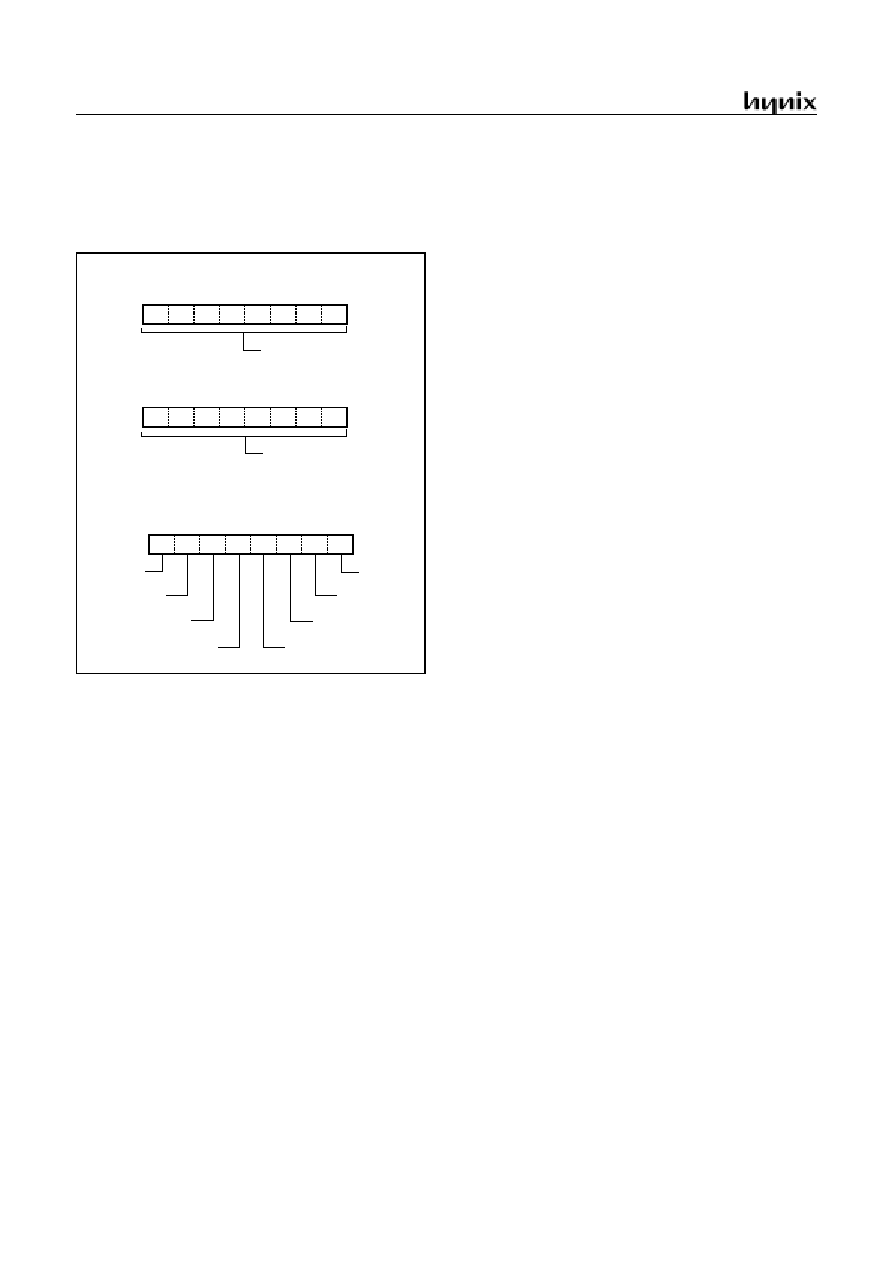
GMS81C2112/GMS81C2120
36
JUNE. 2001 Ver 1.00
tion such as Analog Input, write "1" to the corresponding
bit of R6FUNC. Regardless of the direction register R6IO,
R6FUNC is selected to use as alternate functions, port pin
can be used as a corresponding alternate features
(AN7~AN0)
R6 Function Selection Register
R6FUNC
ADDRESS : 0F7
H
RESET VALUE : 00
H
0: R60
1: AN0
0
0: R61
1: AN1
0: R63
1: AN3
0: R62
1: AN2
1
2
3
4
5
6
7
0: R65
1: AN5
0: R64
1: AN4
0: R66
1: AN6
0: R67
1: AN7
R6 Data Register
R6
ADDRESS: 0CC
H
RESET VALUE: Undefined
R67 R66 R65 R64 R63 R62 R61 R60
Input / Output data
R6 Direction Register
R6IO
ADDRESS : 0CD
H
RESET VALUE : 00
H
Port Direction
0: Input
1: Output
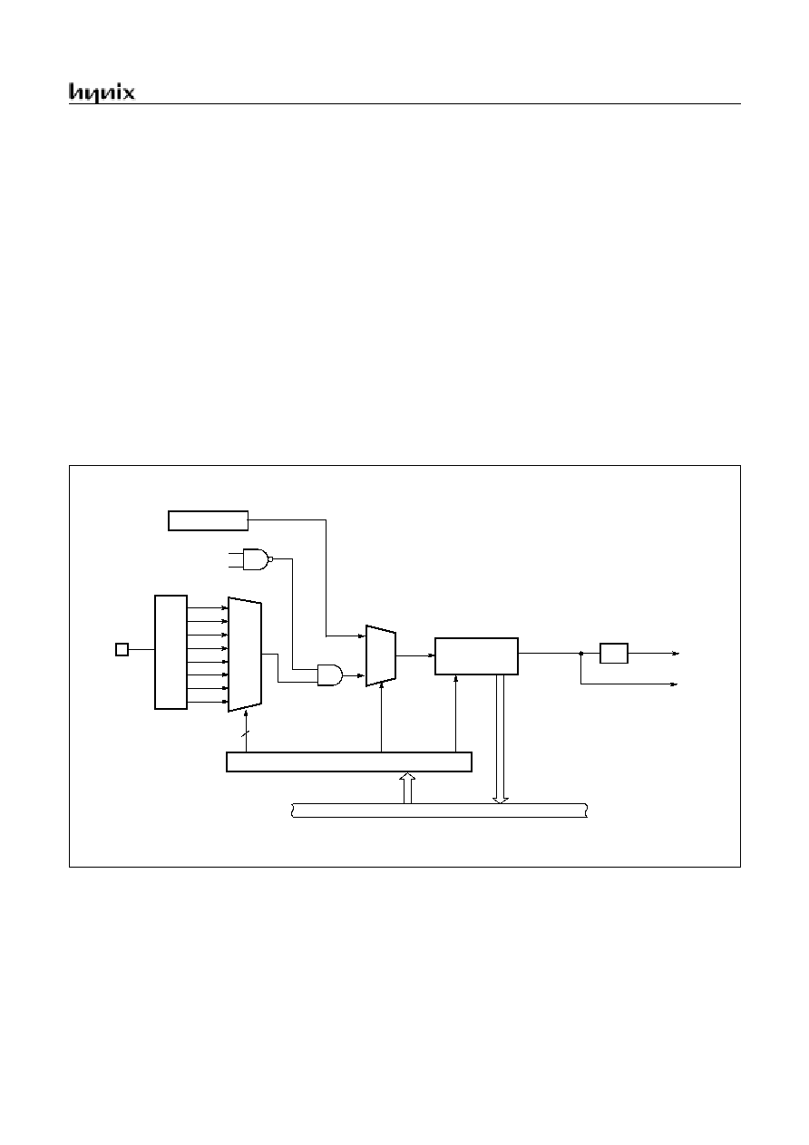
GMS81C2112/GMS81C2120
JUNE. 2001 Ver 1.00
37
10. BASIC INTERVAL TIMER
The GMS81C21xx has one 8-bit Basic Interval Timer that
is free-run, can not stop. Block diagram is shown in Figure
10-1. In addition, the Basic Interval Timer generates the
time base for watchdog timer counting. It also provides a
Basic interval timer interrupt (BITIF).
The 8-bit Basic interval timer register (BITR) is increased
every internal count pulse which is divided by prescaler.
Since prescaler has divided ratio by 8 to 1024, the count
rate is 1/8 to 1/1024 of the oscillator frequency. As the
count overflows from FF
H
to 00
H
, this overflow causes to
generate the Basic interval timer interrupt. The BITIF is in-
terrupt request flag of Basic interval timer. The Basic In-
terval Timer is controlled by the clock control register
(CKCTLR) shown in Figure 10-2.
When write "1" to bit BTCL of CKCTLR, BITR register is
cleared to "0" and restart to count-up. The bit BTCL be-
comes "0" after one machine cycle by hardware.
If the STOP instruction executed after writing "1" to bit
WAKEUP of CKCTLR, it goes into the wake-up timer
mode. In this mode, all of the block is halted except the os-
cillator, prescaler (only fXIN
÷
2048) and Timer0.
If the STOP instruction executed after writing "1" to bit
RCWDT of CKCTLR, it goes into the internal RC oscillat-
ed watchdog timer mode. In this mode, all of the block is
halted except the internal RC oscillator, Basic Interval
Timer and Watchdog Timer. More detail informations are
explained in Power Saving Function. The bit WDTON de-
cides Watchdog Timer or the normal 7-bit timer.
Source clock can be selected by lower 3 bits of CKCTLR.
BITR and CKCTLR are located at same address, and ad-
dress 0EC
H
is read as a BITR, and written to CKCTLR.
Figure 10-1 Block Diagram of Basic Interval Timer
MUX
Basic Interval
BITR
Select Input clock 3
Basic Interval Timer
source
clock
8-bit up-counter
BTS[2:0]
BTCL
÷
1024
÷
512
÷
256
÷
128
÷
64
÷
32
÷
16
÷
8
To Watchdog timer (WDTCK)
CKCTLR
clear
overflow
Internal bus line
clock control register
[0EC
H
]
[0EC
H
]
BITIF
Read
X
IN
PIN
Pre
scale
r
Timer Interrupt
Internal RC OSC
RCWDT
1
0
WAKEUP
STOP
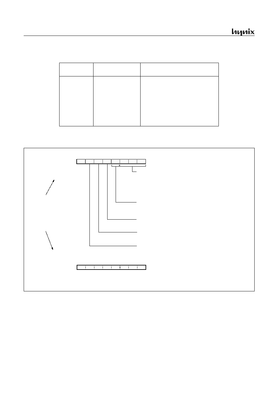
GMS81C2112/GMS81C2120
38
JUNE. 2001 Ver 1.00
Table 10-1 Basic Interval Timer Interrupt Time
Figure 10-2 BITR: Basic Interval Timer Mode Register
Example 1:
Basic Interval Timer Interrupt request flag is generated
every 4.096ms at 4MHz.
:
LDM
CKCTLR,#03H
SET1
BITE
EI
:
Example 2:
Basic Interval Timer Interrupt request flag is generated
every 1.024ms at 4MHz.
:
LDM
CKCTLR,#01H
SET1
BITE
EI
:
CKCTLR
[2:0]
Source clock
Interrupt (overflow) Period (ms)
@ f
XIN
= 4MHz
000
001
010
011
100
101
110
111
f
XIN
÷
8
f
XIN
÷
16
f
XIN
÷
32
f
XIN
÷
64
f
XIN
÷
128
f
XIN
÷
256
f
XIN
÷
512
f
XIN
÷
1024
0.512
1.024
2.048
4.096
8.192
16.384
32.768
65.536
BTCL
7
6
5
4
3
2
1
0
RCWDT
-
BTS1
Basic Interval Timer source clock select
000: f
XIN
÷
8
001: f
XIN
÷
16
010: f
XIN
÷
32
011: f
XIN
÷
64
100: f
XIN
÷
128
101: f
XIN
÷
256
110: f
XIN
÷
512
111: f
XIN
÷
1024
Clear bit
0: Normal operation (free-run)
1: Clear 8-bit counter (BITR) to "0". This bit becomes 0 automatically
INITIAL VALUE: -001 0111
B
ADDRESS: 0EC
H
after one machine cycle, and starts counting.
CKCTLR
INITIAL VALUE: Undefined
ADDRESS: 0EC
H
BITR
Both register are in same address,
when write, to be a CKCTLR,
when read, to be a BITR.
Caution:
8-BIT FREE-RUN BINARY COUNTER
WDTON
BTS0
BTS2
BTCL
BTCL
7
6
5
4
3
2
1
0
0: Operate as a 7-bit general timer
1: Enable Watchdog Timer operation
See the section "Watchdog Timer".
WAKEUP
0: Disable Wake-up Timer
1: Enable Wake-up Timer
0: Disable Internal RC Watchdog Timer
1: Enable Internal RC Watchdog Timer
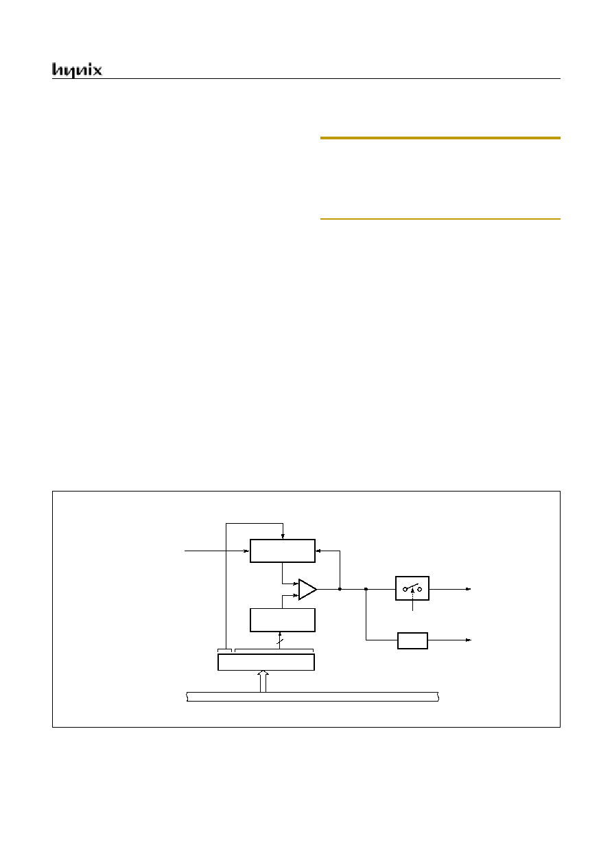
GMS81C2112/GMS81C2120
JUNE. 2001 Ver 1.00
39
11. WATCHDOG TIMER
The watchdog timer rapidly detects the CPU malfunction
such as endless looping caused by noise or the like, and re-
sumes the CPU to the normal state.
The watchdog timer signal for detecting malfunction can
be selected either a reset CPU or a interrupt request.
When the watchdog timer is not being used for malfunc-
tion detection, it can be used as a timer to generate an in-
terrupt at fixed intervals. The purpose of the watchdog
timer is to detect the malfunction (runaway) of program
due to external noise or other causes and return the opera-
tion to the normal condition.
The watchdog timer has two types of clock source.
The first type is an on-chip RC oscillator which does not
require any external components. This RC oscillator is sep-
arate from the external oscillator of the Xin pin. It means
that the watchdog timer will run, even if the clock on the
Xin pin of the device has been stopped, for example, by en-
tering the STOP mode.
The other type is a prescaled system clock.
The watchdog timer consists of 7-bit binary counter and
the watchdog timer data register. When the value of 7-bit
binary counter is equal to the lower 7 bits of WDTR, the
interrupt request flag is generated. This can be used as
WDT interrupt or reset the CPU in accordance with the bit
WDTON.
Note: Because the watchdog timer counter is enabled af-
ter clearing Basic Interval Timer, after the bit WDTON set to
"1", maximum error of timer is depend on prescaler ratio of
Basic Interval Timer. The 7-bit binary counter is cleared by
setting WDTCL(bit7 of WDTR) and the WDTCL is cleared
automatically after 1 machine cycle.
The RC oscillated watchdog timer is activated by setting
the bit RCWDT as shown below.
LDM
CKCTLR,#3FH; enable the RC-osc WDT
LDM
WDTR,#0FFH; set the WDT period
STOP
; enter the STOP mode
NOP
NOP
; RC-osc WDT running
:
The RCWDT oscillation period is vary with temperature,
VDD and process variations from part to part (approxi-
mately, 40~120uS). The following equation shows the
RCWDT oscillated watchdog timer time-out.
T
R C W D T
= C L K
R C W D T
×2
8
×[
W D T R .6 ~ 0 ]+ (C L K
R C W D T
×2
8
)/2
w h ere, C L K
R C W D T
= 4 0 ~ 1 2 0 u S
In addition, this watchdog timer can be used as a simple 7-
bit timer by interrupt WDTIF. The interval of watchdog
timer interrupt is decided by Basic Interval Timer. Interval
equation is as below.
T
WDT
= [WDTR.6~0]
×
×
×
×
Interval of BIT
Figure 11-1 Block Diagram of Watchdog Timer
to reset CPU
BASIC INTERVAL TIMER
Count
enable
Watchdog
7-bit compare data
comparator
Watchdog Timer interrupt
clear
clear
WDTIF
Counter (7-bit)
WDTCL
"0"
"1"
WDTON in CKCTLR [0EC
H
]
OVERFLOW
Watchdog Timer
Register
WDTR
Internal bus line
7
[0ED
H
]
source
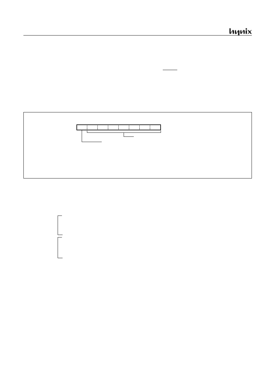
GMS81C2112/GMS81C2120
40
JUNE. 2001 Ver 1.00
Watchdog Timer Control
Figure 11-2 shows the watchdog timer control register.
The watchdog timer is automatically disabled after reset.
The CPU malfunction is detected during setting of the de-
tection time, selecting of output, and clearing of the binary
counter. Clearing the binary counter is repeated within the
detection time.
If the malfunction occurs for any cause, the watchdog tim-
er output will become active at the rising overflow from
the binary counters unless the binary counter is cleared. At
this time, when WDTON=1, a reset is generated, which
drives the RESET pin to low to reset the internal hardware.
When WDTON=0, a watchdog timer interrupt (WDTIF) is
generated.
The watchdog timer temporarily stops counting in the
STOP mode, and when the STOP mode is released, it au-
tomatically restarts (continues counting).
Figure 11-2 WDTR: Watchdog Timer Data Register
Example: Sets the watchdog timer detection time to 0.5 sec at 4.19MHz
7
6
5
4
3
2
1
0
Clear count flag
0: Free-run count
INITIAL VALUE: 0111_1111
B
ADDRESS: 0ED
H
WDTR
W
W
W
W
1: When the WDTCL is set to "1", binary counter
is cleared to "0". And the WDTCL becomes "0" automatically
after one machine cycle. Counter count up again.
7-bit compare data
W
W
W
W
NOTE:
The WDTON bit is in register CKCTLR.
W DTCL
LDM
CKCTLR,#3FH
;
Select 1/2048 clock source
,
WDTON
1, Clear Counter
LDM
WDTR,#04FH
LDM
WDTR,#04FH
;
Clear counter
:
:
:
:
LDM
WDTR,#04FH
;
Clear counter
:
:
:
:
LDM
WDTR,#04FH
;
Clear counter
Within WDT
detection time
Within WDT
detection time
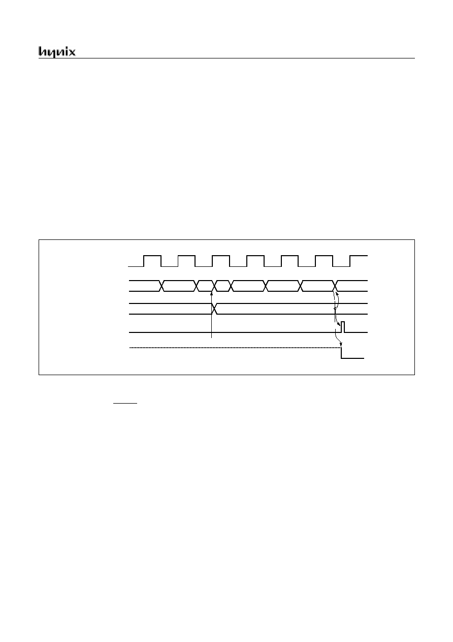
GMS81C2112/GMS81C2120
JUNE. 2001 Ver 1.00
41
Enable and Disable Watchdog
Watchdog timer is enabled by setting WDTON (bit 4 in
CKCTLR) to "1". WDTON is initialized to "0" during re-
set and it should be set to "1" to operate after reset is re-
leased.
Example: Enables watchdog timer for Reset
:
LDM
CKCTLR,#xx1x_xxxxB;
WDTON
1
:
:
The watchdog timer is disabled by clearing bit 5 (WD-
TON) of CKCTLR. The watchdog timer is halted in STOP
mode and restarts automatically after STOP mode is re-
leased.
Watchdog Timer Interrupt
The watchdog timer can be also used as a simple 7-bit tim-
er by clearing bit5 of CKCTLR to "0". The interval of
watchdog timer interrupt is decided by Basic Interval Tim-
er. Interval equation is shown as below.
The stack pointer (SP) should be initialized before using
the watchdog timer output as an interrupt source.
Example: 7-bit timer interrupt set up.
LDM
CKCTLR,#xx0xxxxxB;
WDTON
0
LDM
WDTR,#7FH
;
WDTCL
1
:
Figure 11-3 Watchdog timer Timing
If the watchdog timer output becomes active, a reset is gen-
erated, which drives the RESET pin low to reset the inter-
nal hardware.
The main clock oscillator also turns on when a watchdog
timer reset is generated in sub clock mode.
T
W DTR
Interval of BIT
×
=
2
3
n
Source clock
Binary-counter
WDTR
WDTIF interrupt
WDTR
"0100_0011
B
"
1
0
Match
Detect
Counter
Clear
1
2
3
0
BIT overflow
3
WDT reset
reset
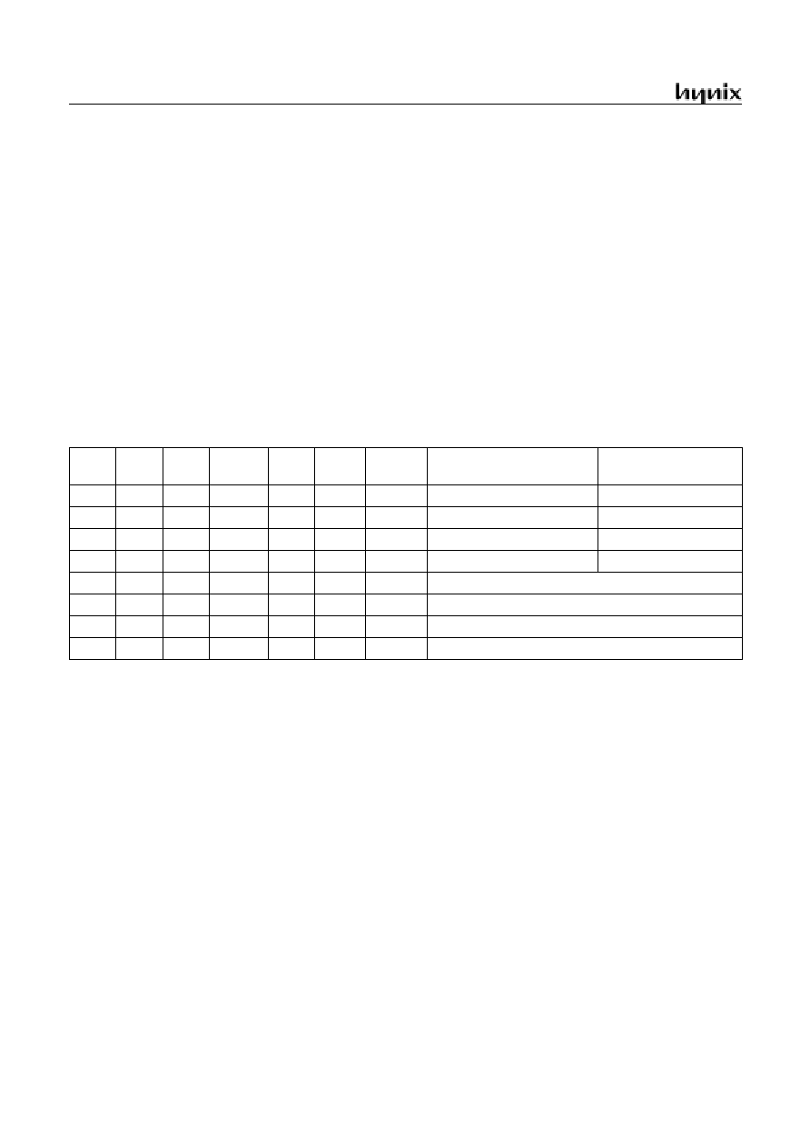
GMS81C2112/GMS81C2120
42
JUNE. 2001 Ver 1.00
12. TIMER/EVENT COUNTER
The GMS81C21xx has two Timer/Counter registers. Each
module can generate an interrupt to indicate that an event
has occurred (i.e. timer match).
Timer 0 and Timer 1 are can be used either two 8-bit Tim-
er/Counter or one 16-bit Timer/Counter with combine
them.
In the "timer" function, the register is increased every in-
ternal clock input. Thus, one can think of it as counting in-
ternal clock input. Since a least clock consists of 2 and
most clock consists of 2048 oscillator periods, the count
rate is 1/2 to 1/2048 of the oscillator frequency in Timer0.
And Timer1 can use the same clock source too. In addition,
Timer1 has more fast clock source (1/1 to 1/8).
In the "counter" function, the register is increased in re-
sponse to a 1-to-0 (falling edge) or 0-to-1(rising edge) tran-
sition at its corresponding external input pin, EC0.
In addition the "capture" function, the register is increased
in response external or internal clock sources same with
timer or counter function. When external clock edge input,
the count register is captured into capture data register
CDRx.
Timer1 is shared with "PWM" function and "Compare out-
put" function
It has seven operating modes: "8-bit timer/counter", "16-
bit timer/counter", "8-bit capture", "16-bit capture", "8-bit
compare output", "16-bit compare output" and "10-bit
PWM" which are selected by bit in Timer mode register
TM0 and TM1 as shown in Figure 12-1 and Table 12-1.
16BIT
CAP0
CAP1
PWM1E
T0CK
[2:0]
T1CK
[1:0]
PWM1O
TIMER 0
TIMER 1
0
0
0
0
XXX
XX
0
8-bit Timer
8-bit Timer
0
0
1
0
111
XX
0
8-bit Event counter
8-bit Capture
0
1
0
0
XXX
XX
1
8-bit Capture (internal clock)
8-bit Compare Output
0
X
0
1
XXX
XX
1
8-bit Timer/Counter
10-bit PWM
1
0
0
0
XXX
11
0
16-bit Timer
1
0
0
0
111
11
0
16-bit Event counter
1
1
X
0
XXX
11
0
16-bit Capture (internal clock)
1
0
0
0
XXX
11
1
16-bit Compare Output
Table 12-1 Operating Modes of Timer0 and Timer1
GMS81C2112/GMS81C2120
JUNE. 2001 Ver 1.00
43
Figure 12-1 TM0, TM1 Registers
BTCL
7
6
5
4
3
2
1
0
16BIT
POL
T1CN
INITIAL VALUE: 00
H
ADDRESS: 0D2
H
TM1
T1ST
T1CK0
T1CK1
PWM1E
CAP1
Bit Name
Bit Position
Description
POL
TM1.7
0: PWM Duty Active Low
1: PWM Duty Active High
16BIT
TM1.6
0: 8-bit Mode
1: 16-bit Mode
PWMIE
TM1.5
0: Disable PWM
1: Enable PWM
CAP1
TM1.4
0: Timer/Counter mode
1: Capture mode selection flag
T1CK1
T1CK0
TM1.3
TM1.2
00: 8-bit Timer, Clock source is f
XIN
01: 8-bit Timer, Clock source is f
XIN
÷
2
10: 8-bit Timer, Clock source is f
XIN
÷
8
11: 8-bit Timer, Clock source is Using the the Timer 0 Clock
T0CN
TM1.1
0: Stop the timer
1: A logic 1 starts the timer.
T0ST
TM1.0
0: When cleared, stop the counting.
1: When set, Timer 0 Count Register is cleared and start again.
BT C L
5
4
3
2
1
0
-
-
T 0C N
IN ITIAL V ALU E: --000000
B
AD D R ES S: 0D 0
H
TM0
T0ST
T 0C k0
T0C K1
C A P0
T 0C k2
Bit Name
Bit Position
Description
CAP0
TM0.5
0: Timer/Counter mode
1: Capture mode selection flag
T0CK2
T0CK1
T0CK0
TM0.4
TM0.3
TM0.2
000: 8-bit Timer, Clock source is f
XIN
÷
2
001: 8-bit Timer, Clock source is f
XIN
÷
4
010: 8-bit Timer, Clock source is f
XIN
÷
8
011: 8-bit Timer, Clock source is f
XIN
÷
32
100: 8-bit Timer, Clock source is f
XIN
÷
128
101: 8-bit Timer, Clock source is f
XIN
÷
512
110: 8-bit Timer, Clock source is f
XIN
÷
2048
111: EC0 (External clock)
T0CN
TM0.1
0: Stop the timer
1: A logic 1 starts the timer.
T0ST
TM0.0
0: When cleared, stop the counting.
1: When set, Timer 0 Count Register is cleared and start again.
7
6
5
4
3
2
1
0
INITIAL VALUE: Undefined
ADDRESS: 0D1
H
TDR0
Read: Count value read
Write: Compare data write
R/W R/W R/W R/W R/W R/W R/W R/W
R/W
R/W
R/W
R/W
R/W
R/W
R/W
R/W
R/W
R/W
R/W
R/W
R/W
R/W
7
6
5
4
3
2
1
0
INITIAL VALUE: Undefined
ADDRESS: 0D3
H
TDR1
R/W R/W R/W R/W R/W R/W R/W R/W
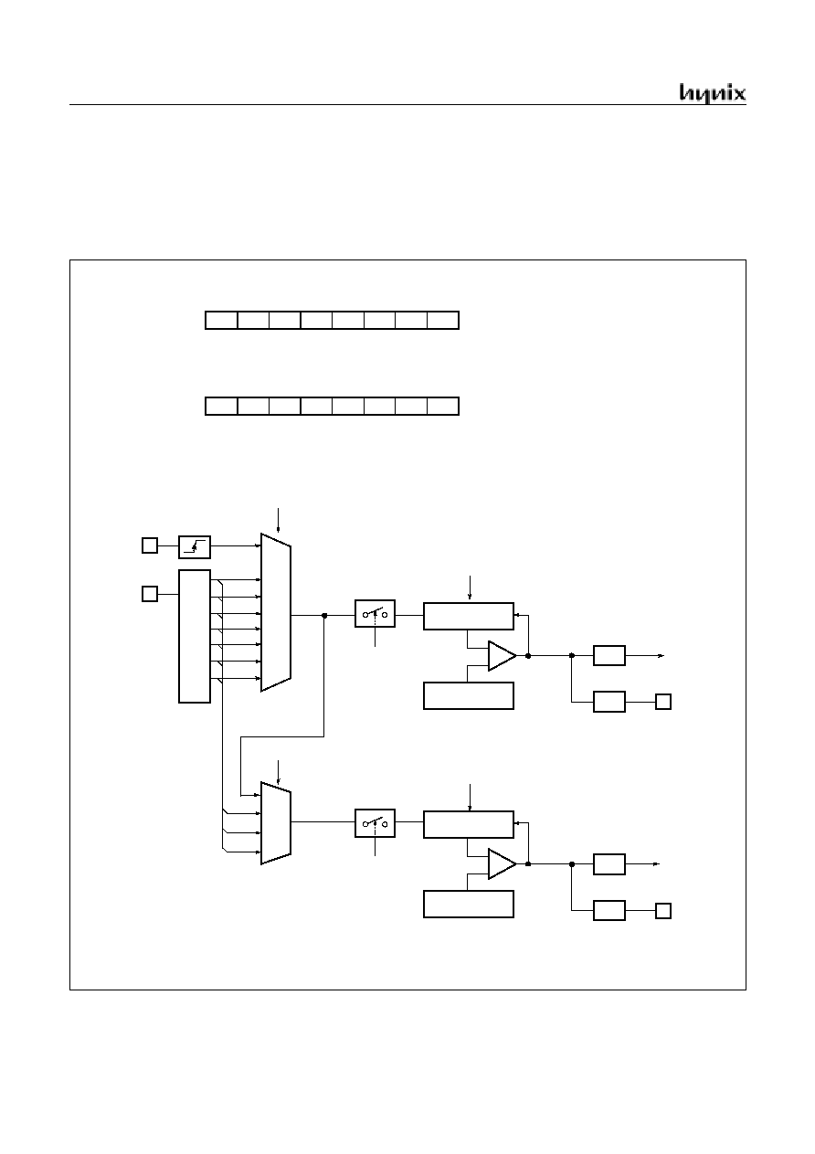
GMS81C2112/GMS81C2120
44
JUNE. 2001 Ver 1.00
12.1 8-bit Timer / Counter Mode
The GMS81C21xx has two 8-bit Timer/Counters, Timer 0,
Timer 1 as shown in Figure 12-2.
The "timer" or "counter" function is selected by mode reg-
isters TMx as shown in Figure 12-1 and Table 12-1. To use
as an 8-bit timer/counter mode, bit CAP0 of TM0 is
cleared to "0" and bits 16BIT of TM1 should be cleared to
"0"(Table 12-1).
Figure 12-2 8-bit Timer/Counter 0, 1
EC0 PIN
÷
2
÷
4
÷
8
XIN PIN
MUX
Pr
esca
ler
clear
0: Stop
1: Clear and start
T0ST
T0CK[2:0]
111
000
001
010
T0CN
MUX
T1IF
clear
0: Stop
1: Clear and start
T1ST
T1CK[1:0]
11
00
01
TIMER 1
INTERRUPT
÷
1
÷
2
÷
8
TDR0 (8-bit)
TDR1 (8-bit)
T1 (8-bit)
T0 (8-bit)
Comparator
Comparator
TIMER 0
TIMER 1
T1O PIN
F/F
BTCL
7
6
5
4
3
2
1
0
-
-
T0CN
INITIAL VALUE: --000000
B
ADDRESS: 0D0
H
TM0
T0ST
T0CK0
T0CK1
CAP0 T0CK2
-
-
X
X
X
X
X means don't care
÷
÷
÷
512
÷
2048
011
100
101
110
T0IF
TIMER 0
INTERRUPT
T0O PIN
F/F
T1CN
10
INITIAL VALUE: 00
H
ADDRESS: 0D2
H
TM1
X means don't care
0
X
BTCL
7
6
5
4
3
2
1
0
16BIT
POL
T1CN T1ST
T1CK0
T1CK1
PWM1E
CAP1
X
0
X
X
X
X
0
0
EDGE
DETECTOR

GMS81C2112/GMS81C2120
JUNE. 2001 Ver 1.00
45
Example 1:
Timer0 = 2ms 8-bit timer mode at 4MHz
Timer1 = 0.5ms 8-bit timer mode at 4MHz
LDM
TDR0,#250
LDM
TDR1,#250
LDM
TM0,#0000_1111B
LDM
TM1,#0000_1011B
SET1
T0E
SET1
T1E
EI
Example 2:
Timer0 = 8-bit event counter mode
Timer1 = 0.5ms 8-bit timer mode at 4MHz
LDM
TDR0,#250
LDM
TDR1,#250
LDM
TM0,#0001_1111B
LDM
TM1,#0000_1011B
SET1
T0E
SET1
T1E
EI
Note: The contents of Timer data register TDRx should be
initialized 1
H
~FF
H
, not 0
H
, because it is undefined after re-
set.
These timers have each 8-bit count register and data regis-
ter. The count register is increased by every internal or ex-
ternal clock input. The internal clock has a prescaler divide
ratio option of 2, 4, 8, 32,128, 512, 2048 selected by con-
trol bits T0CK[2:0] of register (TM0) and 1, 2, 8 selected
by control bits T1CK[1:0] of register (TM1). In the Timer
0, timer register T0 increases from 00
H
until it matches
TDR0 and then reset to 00
H
. The match output of Timer 0
generates Timer 0 interrupt (latched in T0IF bit). As TDRx
and Tx register are in same address, when reading it as a
Tx, written to TDRx.
In counter function, the counter is increased every 0-to-
1(1-to-0) (rising & falling edge) transition of EC0 pin. In
order to use counter function, the bit EC0 of the R0
Func-
tion Selection
Register
(R0FUNC.2) is set to "1". The Timer
0 can be used as a counter by pin EC0 input, but Timer 1
can not.
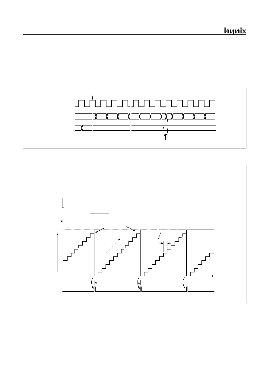
GMS81C2112/GMS81C2120
46
JUNE. 2001 Ver 1.00
8-bit Timer Mode
In the timer mode, the internal clock is used for counting
up. Thus, you can think of it as counting internal clock in-
put. The contents of TDRn are compared with the contents
of up-counter, Tn. If match is found, a timer 1 interrupt
(T1IF) is generated and the up-counter is cleared to 0.
Counting up is resumed after the up-counter is cleared.
As the value of TDRn is changeable by software, time in-
terval is set as you want
Figure 12-3 Timer Mode Timing Chart
Figure 12-4 Timer Count Example
0
n-2
2
0
n
3
n-1
n
Source clock
Up-counter
TDR1
T1IF interrupt
Start count
1
2
3
1
4
Match
Detect
Counter
Clear
~~
~~
~~
~~
~~
~~
Timer 1 (T1IF)
Interrupt
TDR1
TIME
Occur interrupt
Occur interrupt
Occur interrupt
Interrupt period
up-
count
~~
~~
0
1
2
3
4
5
6
7A
7D
7C
Count Pulse
= 8
µ
s x 125
7B
MATCH
Example: Make 2ms
interrupt using by Timer0 at 4MHz
LDM
TM0,#0FH
; divide by 32
LDM
TDR0,#125
; 8us x 125= 1ms
SET1
T0E
; Enable Timer 0 Interrupt
EI
; Enable Master Interrupt
Period
When
TDR0 = 125
D
= 7D
H
f
XIN
= 4 MHz
INTERRUPT PERIOD =
4
×
10
6
Hz
1
×
32
×
125 = 1 ms
TM0 = 0000 1111
B
(8-bit Timer mode, Prescaler divide ratio = 32)
8
µ
s
(TDR0 = T0)
7D
0
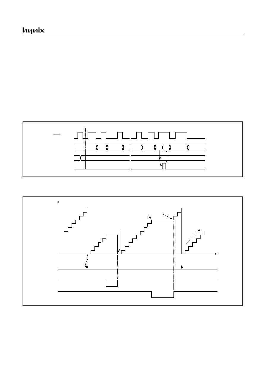
GMS81C2112/GMS81C2120
JUNE. 2001 Ver 1.00
47
8-bit Event Counter Mode
In this mode, counting up is started by an external trigger.
This trigger means falling edge or rising edge of the EC0
pin input. Source clock is used as an internal clock selected
with timer mode register TM0. The contents of timer data
register TDR0 is compared with the contents of the up-
counter T0. If a match is found, an timer interrupt request
flag T0IF is generated, and the counter is cleared to "0".
The counter is restart and count up continuously by every
falling edge or rising edge of the EC0 pin input.
The maximum frequency applied to the EC0 pin is f
XIN
/2
[Hz].
In order to use event counter function, the bit 2 of the R5
function register (R5FUNC.2) is required to be set to "1".
After reset, the value of timer data register TDR0 is unde-
fined, it should be initialized to between 1
H
~FF
H
not to
"0"The interval period of Timer is calculated as below
equation.
Figure 12-5 Event Counter Mode Timing Chart
Figure 12-6 Count Operation of Timer / Event counter
Period (sec)
1
f
XIN
-----------
2
Divide Ratio
TDR0
×
×
×
=
0
1
2
1
0
n
2
~~
~~
~~
n-1
n
~~
~~
~~
ECn pin input
Up-counter
TDR1
T1IF interrupt
Start count
Timer 1 (T1IF)
Interrupt
TDR1
TIME
Occur interrupt
Occur interrupt
stop
clear & start
disable
enable
Start & Stop
T1ST
T1CN
Control count
up
-c
oun
t
~~
~~
T1ST = 0
T1ST = 1
T1CN = 0
T1CN = 1
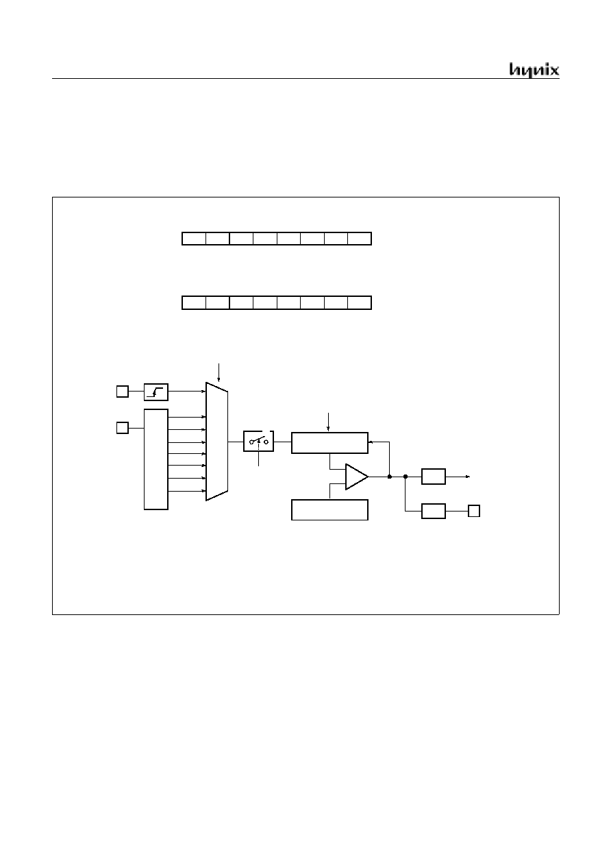
GMS81C2112/GMS81C2120
48
JUNE. 2001 Ver 1.00
12.2 16-bit Timer / Counter Mode
The Timer register is being run with 16 bits. A 16-bit timer/
counter register T0, T1 are increased from 0000
H
until it
matches TDR0, TDR1 and then resets to 0000
H
. The
match output generates Timer 0 interrupt not Timer 1 in-
terrupt.
The clock source of the Timer 0 is selected either internal
or external clock by bit T0CK[2:0].
In 16-bit mode, the bits T1CK[1:0] and 16BIT of TM1
should be set to "1" respectively.
Figure 12-7 16-bit Timer/Counter
clear
0: Stop
1: Clear and start
T0ST
T0CN
TDR1 + TDR0
Comparator
TIMER 0 + TIMER 1
TIMER 0 (16-bit)
Higher byte Lower byte
(16-bit)
COMPARE DATA
T1 + T0
(16-bit)
1
0
(Not Timer 1 interrupt)
EDGE
BTCL
7
6
5
4
3
2
1
0
-
-
T0CN
INITIAL VALUE: --000000
B
ADDRESS: 0D0
H
TM0
T0ST
T0CK0
T0CK1
CAP0 T0CK2
-
-
X
X
X
X
X means don't care
INITIAL VALUE: 00
H
ADDRESS: 0D2
H
TM1
X means don't care
0
X
BTCL
7
6
5
4
3
2
1
0
16BIT
POL
T1CN T1ST
T1CK0
T1CK1
PWM1E
CAP1
X
1
X
X
1
1
0
0
EC0 PIN
÷
2
÷
4
÷
8
XIN PIN
MUX
Pr
esca
ler
T0CK[2:0]
111
000
001
010
÷
÷
÷
512
÷
2048
011
100
101
110
DETECTOR
T0IF
TIMER 0
INTERRUPT
T0O PIN
F/F

GMS81C2112/GMS81C2120
JUNE. 2001 Ver 1.00
49
12.3 8-bit Compare Output (16-bit)
The GMS81C21xx has a function of Timer Compare Out-
put. To pulse out, the timer match can goes to port
pin(T0O, T1O) as shown in Figure 12-2 and Figure 12-7.
Thus, pulse out is generated by the timer match. These op-
eration is implemented to pin, T0O, PWM1O/T1O.
In this mode, the bit PWM1O/T1O of R5 function register
(R5FUNC.6) should be set to "1", and the bit PWM1E of
timer1 mode register (TM1) should be set to "0". In addi-
tion, 16-bit Compare output mode is available, also.
This pin output the signal having a 50 : 50 duty square
wave, and output frequency is same as below equation.
12.4 8-bit Capture Mode
The Timer 0 capture mode is set by bit CAP0 of timer
mode register TM0 (bit CAP1 of timer mode register TM1
for Timer 1) as shown in Figure 12-8.
As mentioned above, not only Timer 0 but Timer 1 can also
be used as a capture mode.
The Timer/Counter register is increased in response inter-
nal or external input. This counting function is same with
normal timer mode, and Timer interrupt is generated when
timer register T0 (T1) increases and matches TDR0
(TDR1).
This timer interrupt in capture mode is very useful when
the pulse width of captured signal is more wider than the
maximum period of Timer.
For example, in Figure 12-10, the pulse width of captured
signal is wider than the timer data value (FF
H
) over 2
times. When external interrupt is occurred, the captured
value (13
H
) is more little than wanted value. It can be ob-
tained correct value by counting the number of timer over-
flow occurrence.
Timer/Counter still does the above, but with the added fea-
ture that a edge transition at external input INTx pin causes
the current value in the Timer x register (T0,T1), to be cap-
tured into registers CDRx (CDR0, CDR1), respectively.
After captured, Timer x register is cleared and restarts by
hardware.
Note: The CDRx, TDRx and Tx are in same address. In
the capture mode, reading operation is read the CDRx, not
Tx because path is opened to the CDRx, and TDRx is only
for writing operation.
It has three transition modes: "falling edge", "rising edge",
"both edge" which are selected by interrupt edge selection
register IEDS (Refer to External interrupt section). In ad-
dition, the transition at INTx pin generate an interrupt.
f
C OMP
Oscillation Frequency
2
Prescaler Value
T DR
1
)
+
(
×
×
---------------------------------------------------------------------------------
=
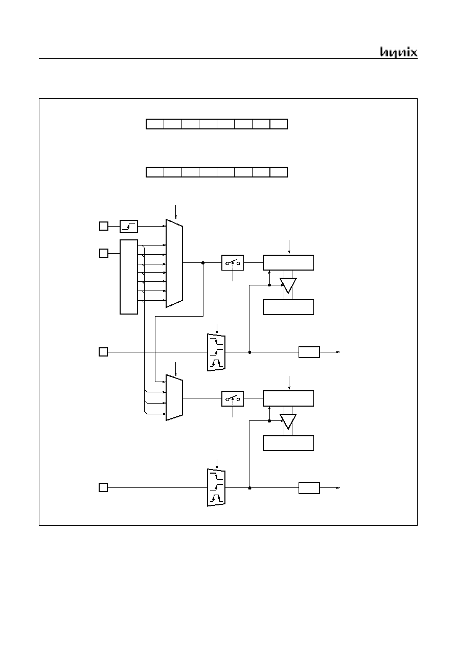
GMS81C2112/GMS81C2120
50
JUNE. 2001 Ver 1.00
.
Figure 12-8 8-bit Capture Mode
INT0IF
0: Stop
1: Clear and start
T0ST
INT0
INTERRUPT
T0CN
CDR0 (8-bit)
T0 (8-bit)
"01"
"10"
"11"
Capture
IEDS[1:0]
EC0 PIN
÷
2
÷
4
÷
8
XIN PIN
MUX
Pre
scale
r
T0CK[2:0]
111
000
001
010
MUX
T1CK[1:0]
11
00
01
÷
1
÷
2
÷
8
÷
÷
÷
512
÷
2048
011
100
101
110
10
INT0 PIN
INT1IF
0: Stop
1: Clear and start
T1ST
INT1
INTERRUPT
T1CN
CDR1 (8-bit)
T1 (8-bit)
"01"
"10"
"11"
Capture
IEDS[1:0]
INT1 PIN
BTCL
7
6
5
4
3
2
1
0
-
-
T0CN
INITIAL VALUE: --000000
B
ADDRESS: 0D0
H
TM0
T0ST
T0CK0
T0CK1
CAP0 T0CK2
-
-
X
X
X
X
X means don't care
INITIAL VALUE: 00
H
ADDRESS: 0D2
H
TM1
X means don't care
1
X
BTCL
7
6
5
4
3
2
1
0
16BIT
POL
T1CN T1ST
T1CK0
T1CK1
PWM1E
CAP1
X
0
X
X
X
X
0
1
Edge
Detector
clear
clear
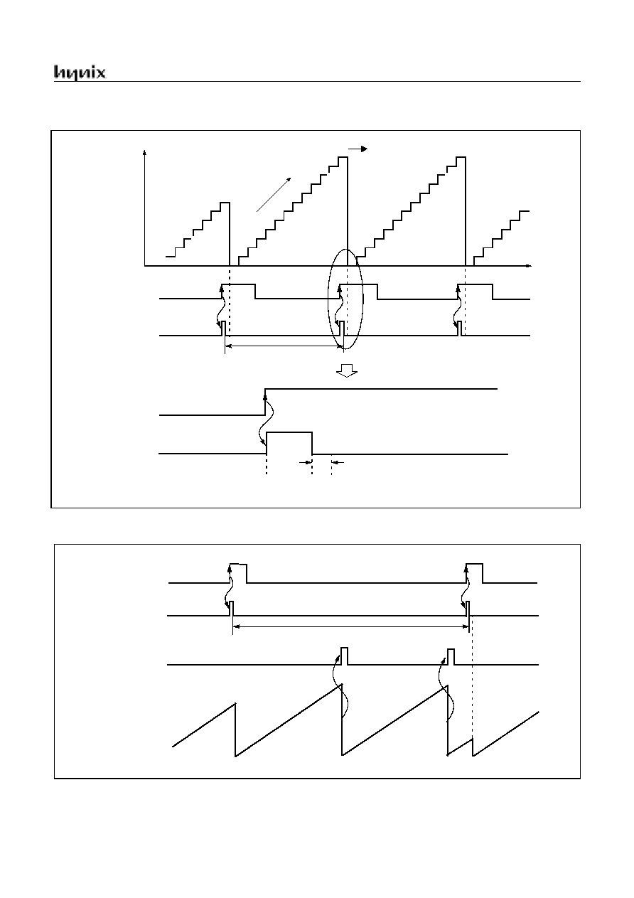
GMS81C2112/GMS81C2120
JUNE. 2001 Ver 1.00
51
Figure 12-9 Input Capture Operation
Figure 12-10 Excess Timer Overflow in Capture Mode
~~
Ext. INT0 Pin
Interrupt Request
T0
TIME
up
-c
oun
t
~~
~~
0
1
2
3
4
5
6
7
8
9
n
n-1
Capture
( Timer Stop )
Clear & Start
Interrupt Interval Period
Delay
( INT0F )
Ext. INT0 Pin
Interrupt Request
( INT0F )
This value is loaded to CDR0
Interrupt Interval Period = FF
H
+ 01
H
+ FF
H
+01
H
+ 13
H
= 213
H
FF
H
FF
H
Ext. INT0 Pin
Interrupt Request
( INT0F )
00
H
00
H
Interrupt Request
( T0F )
T0
13
H
GMS81C2112/GMS81C2120
52
JUNE. 2001 Ver 1.00
12.5 16-bit Capture Mode
16-bit capture mode is the same as 8-bit capture, except
that the Timer register is being run will 16 bits.
The clock source of the Timer 0 is selected either internal
or external clock by bit T0CK2, T0CK1 and T0CK0.
In 16-bit mode, the bits T1CK1,T1CK0 and 16BIT of TM1
should be set to "1" respectively.
Figure 12-11 16-bit Capture Mode
0: Stop
1: Clear and start
T0ST
T0CN
Capture
CDR1 + CDR0
Higher byte Lower byte
(16-bit)
CAPTURE DATA
TDR1 + TDR0
(16-bit)
INT0IF
INT0
INTERRUPT
"01"
"10"
"11"
IEDS[1:0]
EC0 PIN
÷
2
÷
4
÷
8
XIN PIN
MUX
P
r
esca
ler
T0CK[2:0]
111
000
001
010
÷
÷
÷
512
÷
2048
011
100
101
110
INT0 PIN
BTCL
7
6
5
4
3
2
1
0
-
-
T0CN
INITIAL VALUE: --000000
B
ADDRESS: 0D0
H
TM0
T0ST
T0CK0
T0CK1
CAP0 T0CK2
-
-
X
X
X
X
X means don't care
INITIAL VALUE: 00
H
ADDRESS: 0D2
H
TM1
X means don't care
1
X
BTCL
7
6
5
4
3
2
1
0
16BIT
POL
T1CN T1ST
T1CK0
T1CK1
PWM1E
CAP1
X
1
X
X
1
1
0
X
Edge
Detector
clear

GMS81C2112/GMS81C2120
JUNE. 2001 Ver 1.00
53
Example 1:
Timer0 = 16-bit timer mode, 0.5s at 4MHz
LDM
TM0,#0000_1111B;8uS
LDM
TM1,#0100_1100B;16bit Mode
LDM
TDR0,#<62500 ;8uS X 62500
LDM
TDR1,#>62500 ;=0.5s
SET1
T0E
EI
:
:
Example 2:
Timer0 = 16-bit event counter mode
LDM
R0FUNC,#0000_0100B;EC0 Set
LDM
TM0,#0001_1111B;Counter Mode
LDM
TM1,#0100_1100B;16bit Mode
LDM
TDR0,#<0FFH ;
LDM
TDR1,#>0FFH ;
SET1
T0E
EI
:
:
Example 3:
Timer0 = 16-bit capture mode
LDM
R0FUNC,#0000_0001B;INT0 set
LDM
TM0,#0010_1111B;Capture Mode
LDM
TM1,#0100_1100B;16bit Mode
LDM
TDR0,#<0FFH ;
LDM
TDR1,#>0FFH ;
LDM
IEDS,#01H;Falling Edge
SET1
T0E
EI
:
:
12.6 PWM Mode
The GMS81C2120 has a high speed PWM (Pulse Width
Modulation) functions which shared with Timer1.
In PWM mode, pin R56/PWM1O/T1O outputs up to a 10-
bit resolution PWM output. This pin should be configured
as a PWM output by setting "1" bit PWM1O in R5FUNC.6
register.
The period of the PWM output is determined by the
T1PPR (PWM1 Period Register) and PWM1HR[3:2]
(bit3,2 of PWM1 High Register) and the duty of the PWM
output is determined by the T1PDR (PWM1 Duty Regis-
ter) and PWM1HR[1:0] (bit1,0 of PWM1 High Register).
The user writes the lower 8-bit period value to the T1PPR
and the higher 2-bit period value to the PWM1HR[3:2].
A n d w r i t e s d u t y v a l u e t o t h e T 1 P D R a n d t h e
PWM1HR[1:0] same way.
The T1PDR is configured as a double buffering for glitch-
less PWM output. In Figure 12-12, the duty data is trans-
ferred from the master to the slave when the period data
matched to the counted value. (i.e. at the beginning of next
duty cycle)
PWM Period = [PWM1HR[3:2]T1PPR] X Source Clock
PWM Duty = [PWM1HR[1:0]T1PDR] X Source Clock
The relation of frequency and resolution is in inverse pro-
portion. Table 12-2 shows the relation of PWM frequency
vs. resolution.
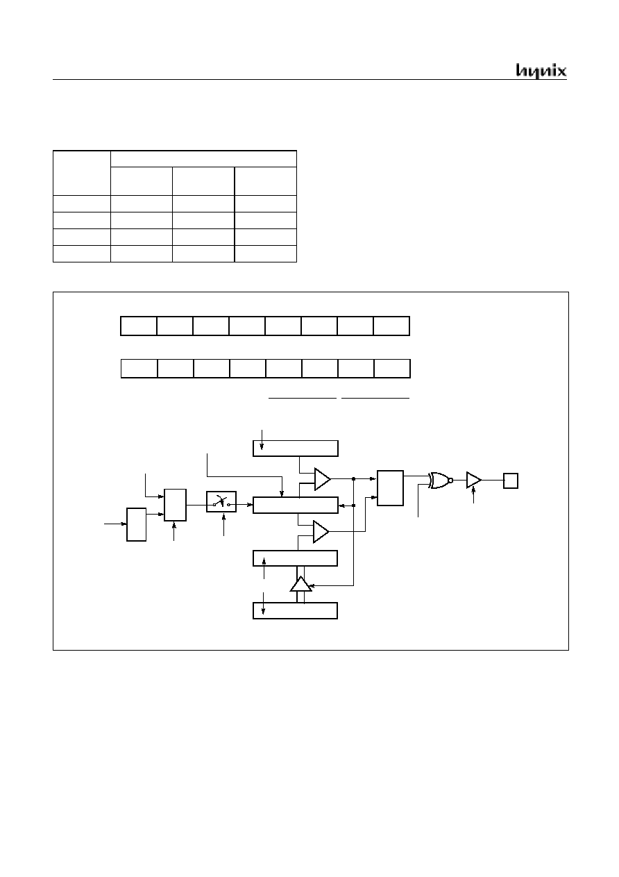
GMS81C2112/GMS81C2120
54
JUNE. 2001 Ver 1.00
If it needed more higher frequency of PWM, it should be
reduced resolution.
The bit POL of TM1 decides the polarity of duty cycle.
If the duty value is set same to the period value, the PWM
output is determined by the bit POL (1: High, 0: Low). And
if the duty value is set to "00
H
", the PWM output is deter-
mined by the bit POL (1: Low, 0: High).
It can be changed duty value when the PWM output. How-
ever the changed duty value is output after the current pe-
riod is over. And it can be maintained the duty value at
present output when changed only period value shown as
Figure 12-14. As it were, the absolute duty time is not
changed in varying frequency. But the changed period val-
ue must greater than the duty value.
Figure 12-12 PWM Mode
Resolution
Frequency
T1CK[1:0]
= 00(250nS)
T1CK[1:0]
= 01(500nS)
T1CK[1:0]
= 10(2uS)
10-bit
3.9KHz
0.98KHZ
0.49KHZ
9-bit
7.8KHz
1.95KHz
0.97KHz
8-bit
15.6KHz
3.90KHz
1.95KHz
7-bit
31.2KHz
7.81KHz
3.90KHz
Table 12-2 PWM Frequency vs. Resolution at 4MHz
÷
1
÷
2
÷
8
PWM1HR
ADDRESS : D5H
RESET VALUE : ----0000
-
-
-
-
PWM1HR3PWM1HR2PWM1HR1PWM1HR0
-
-
-
-
X
X
X
X
MUX
1
T1CN
T1CK[1:0]
T1 ( 8-bit )
T1ST
0 : Stop
1 : Clear and Start
CLEAR
COMPARATOR
COMPARATOR
T1PDR(8-bit)
PWM1HR[1:0]
T1PPR(8-bit)
PWM1HR[3:2]
T1PDR(8-bit)
S
Q
R
POL
PWM1O
R56/
PWM1O/T1O
T0 clock source
f
XI
TM1
ADDRESS : D2H
RESET VALUE : 00000000
POL
16BIT
PWM1E
CAP1
T1CK1
T1CK0
T1CN
T1ST
X
0
1
0
X
X
X
X
[R5FUNC.6]
Period High
Duty High
Slave
Master
Bit Manipulation Not Available
X : The value "0" or "1" corresponding your operation.
[T0CK]
(2-bit)
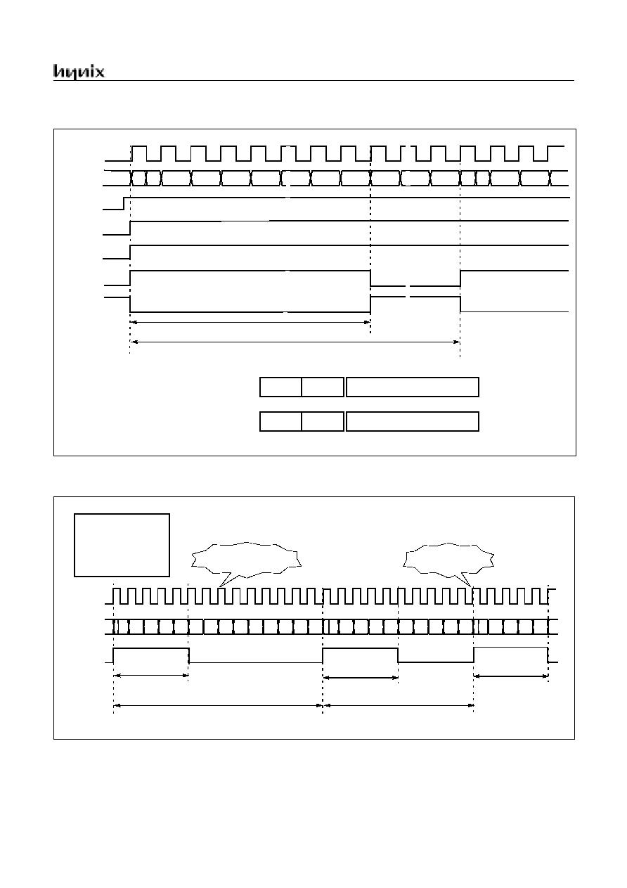
GMS81C2112/GMS81C2120
JUNE. 2001 Ver 1.00
55
Figure 12-13 Example of PWM at 4MHz
Figure 12-14 Example of Changing the Period in Absolute Duty Cycle (@4MHz)
Source
T1
PWM1O
~~
~~
~~
02
03
04
05
7F
80
81
02
03
~~
~~
~~
~~
~~
~~
~~
[POL=1]
PWM1O
[POL=0]
Duty Cycle [ 80H x 250nS = 32uS ]
Period Cycle [ 3FFH x 250nS = 255.75uS, 3.9KHz ]
PWM1HR = 0CH
T1PPR = FFH
T1PDR = 80H
T1CK[1:0] = 00 ( f
XI
)
PWM1HR3 PWM1HR2
PWM1HR1 PWM1HR0
T1PPR (8-bit)
T1PDR (8-bit)
Period
Duty
1
1
FFH
0
0
80H
01
00
clock
PWM1E
~~
T1ST
~~
T1CN
~~
01
00
3FF
Source
T1
PWM1O
POL=1
Duty Cycle
Period Cycle [ 0EH x 2uS = 28uS, 35.5KHz ]
P W M 1 H R = 0 0H
T 1 P P R = 0 E H
T 1 P D R = 0 5H
T 1 C K [1:0 ] = 10 ( 1 u S )
02
03
04
05
06
08
09
0B 0C 0D 0E
01 02
03
04
05
06 07
08
09
0A
01 02
03 04
07
0A
05
[ 05H x 2uS = 10uS ]
Duty Cycle
[ 05H x 2uS = 10uS ]
Period Cycle [ 0AH x 2uS = 20uS, 50KHz ]
Duty Cycle
[ 05H x 2uS = 10uS ]
Write T1PPR to 0AH
Period changed
clock
01
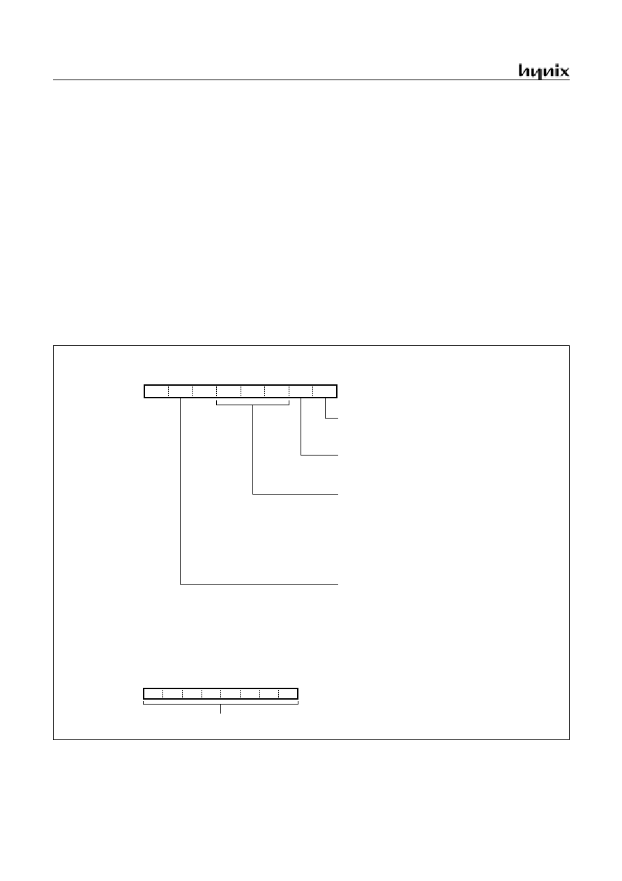
GMS81C2112/GMS81C2120
56
JUNE. 2001 Ver 1.00
13. ANALOG DIGITAL CONVERTER
The analog-to-digital converter (A/D) allows conversion
of an analog input signal to a corresponding 8-bit digital
value. The A/D module has eight analog inputs, which are
multiplexed into one sample and hold. The output of the
sample and hold is the input into the converter, which gen-
erates the result via successive approximation. The analog
supply voltage is connected to AV
DD
of ladder resistance
of A/D module.
The A/D module has two registers which are the control
register ADCM and A/D result register ADR. The register
ADCM, shown in Figure 13-1, controls the operation of
the A/D converter module. The port pins can be configured
as analog inputs or digital I/O.
To use analog inputs, each port is assigned analog input
port by setting the bit ANSEL[7:0] in R6FUNC register.
And selected the corresponding channel to be converted by
setting ADS[3:0].
How to Use A/D Converter
The processing of conversion is start when the start bit
ADST is set to "1". After one cycle, it is cleared by hard-
ware. The register ADCR contains the results of the A/D
conversion. When the conversion is completed, the result
is loaded into the ADCR, the A/D conversion status bit
ADSF is set to "1", and the A/D interrupt flag ADIF is set.
The block diagram of the A/D module is shown in Figure
13-2. The A/D status bit ADSF is set automatically when
A/D conversion is completed, cleared when A/D conver-
sion is in process. The conversion time takes maximum 20
uS (at f
XI
=4 MHz)
Figure 13-1 A/D Converter Control Register
BTCL
7
6
5
4
3
2
1
0
-
ADST
A/D status bit
Analog input channel select
INITIAL VALUE: -0-0 0001
B
ADDRESS: 0EA
H
ADCM
ADSF
A/D converter Enable bit
0: A/D converter module turn off and
current is not flow.
1: Enable A/D converter
R/W
R/W
R/W
R/W
R/W
R
000: Channel 0 (AN0)
001: Channel 1 (AN1)
010: Channel 2 (AN2)
011: Channel 3 (AN3)
100: Channel 4 (AN4)
101: Channel 5 (AN5)
110: Channel 6 (AN6)
111: Channel 7 (AN7)
0: A/D conversion is in progress
1: A/D conversion is completed
A/D start bit
Setting this bit starts an A/D conversion.
After one cycle, bit is cleared to "0" by hardware.
ADS1 ADS0
-
ADS2
INITIAL VALUE: Undefined
ADDRESS: 0EB
H
ADCR
A/D Conversion Data
BTCL
7
6
5
4
3
2
1
0
R
R
R
R
R
R
R
R
ADEN
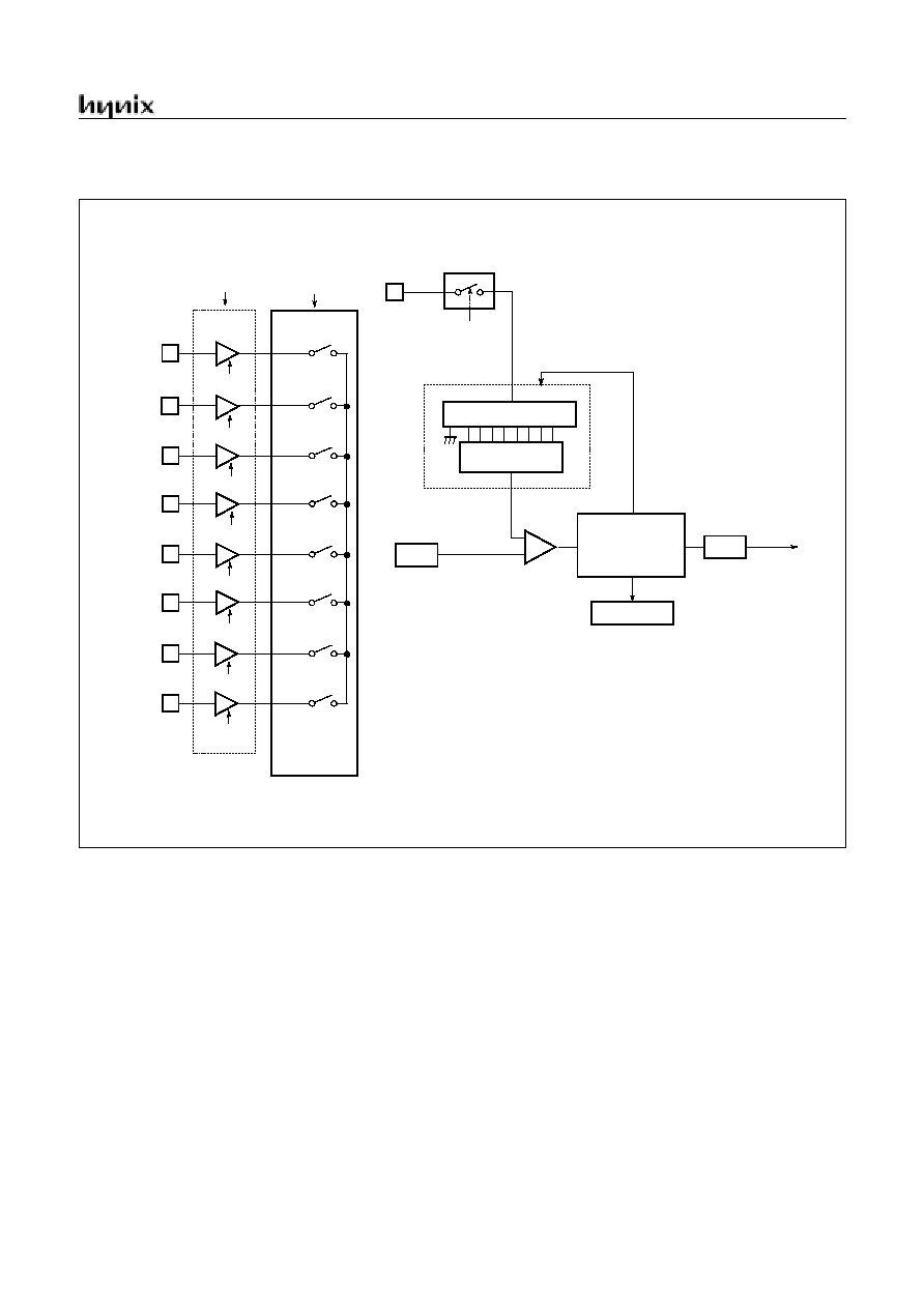
GMS81C2112/GMS81C2120
JUNE. 2001 Ver 1.00
57
.
Figure 13-2 A/D Block Diagram
R60/AN0
S/H
Sample & Hold
"0"
"1"
ADEN
AV
DD
ADIF
A/D
INTERRUPT
SUCCESSIVE
APPROXIMATION
CIRCUIT
ADR (8-bit)
A/D result register
ADDRESS: E9
H
RESET VALUE: Undefined
000
ADS[2:0]
LADDER RESISTOR
8-bit DAC
R61/AN1
001
R62/AN2
010
R63/AN3
011
R64/AN4
100
R65/AN5
101
R66/AN6
110
R67/AN7
111
ANSEL0
R6FUNC[7:0]
ANSEL1
ANSEL2
ANSEL3
ANSEL4
ANSEL5
ANSEL6
ANSEL7
GMS81C2112/GMS81C2120
58
JUNE. 2001 Ver 1.00
Figure 13-3 A/D Converter Operation Flow
A/D Converter Cautions
(1) Input range of AN7 to AN0
The input voltage of AN7 to AN0 should be within the
specification range. In particular, if a voltage above A
VDD
or below AVSS
is input (even if within the absolute maximum
rating range), the conversion value for that channel can not be in-
determinate. The conversion values of the other channels may
also be affected.
(2) Noise countermeasures
In order to maintain 8-bit resolution, attention must be paid to
noise on pins AVDD and AN7 to AN0. Since
the effect increas-
es in proportion to the output impedance of the analog in-
put source, it is recommended that
a capacitor be connected
externally as shown in Figure 13-4 in order to reduce noise.
Figure 13-4 Analog Input Pin Connecting Capacitor
(3) Pins AN7/R67 to AN0/R60
The analog input pins AN7 to AN0 also function as input/
output port (PORT R6) pins. When A/D conversion is per-
formed with any of pins AN7 to AN0 selected, be sure not
to execute a PORT input instruction while conversion is in
progress, as this may reduce the conversion resolution.
Also, if digital pulses are applied to a pin adjacent to the
pin in the process of A/D conversion, the expected A/D
conversion value may not be obtainable due to coupling
noise. Therefore, avoid applying pulses to pins adjacent to
the pin undergoing A/D conversion.
(4) AVDD pin input impedance
A series resistor string of approximately 10K
is connected be-
tween the AVDD
pin and the AVSS
pin.
Therefore, if the output impedance of the reference voltage
source is high, this will result in parallel connection
to the
series resistor string between the AVDD
pin and the AVSS
pin,
and there will be a large reference voltage error.
ENABLE A/D CONVERTER
A/D START ( ADST = 1 )
NOP
ADSF = 1
A/D INPUT CHANNEL SELECT
ANALOG REFERENCE SELECT
READ ADCR
YES
NO
AN11~AN0
100~1000pF
Analog
Input
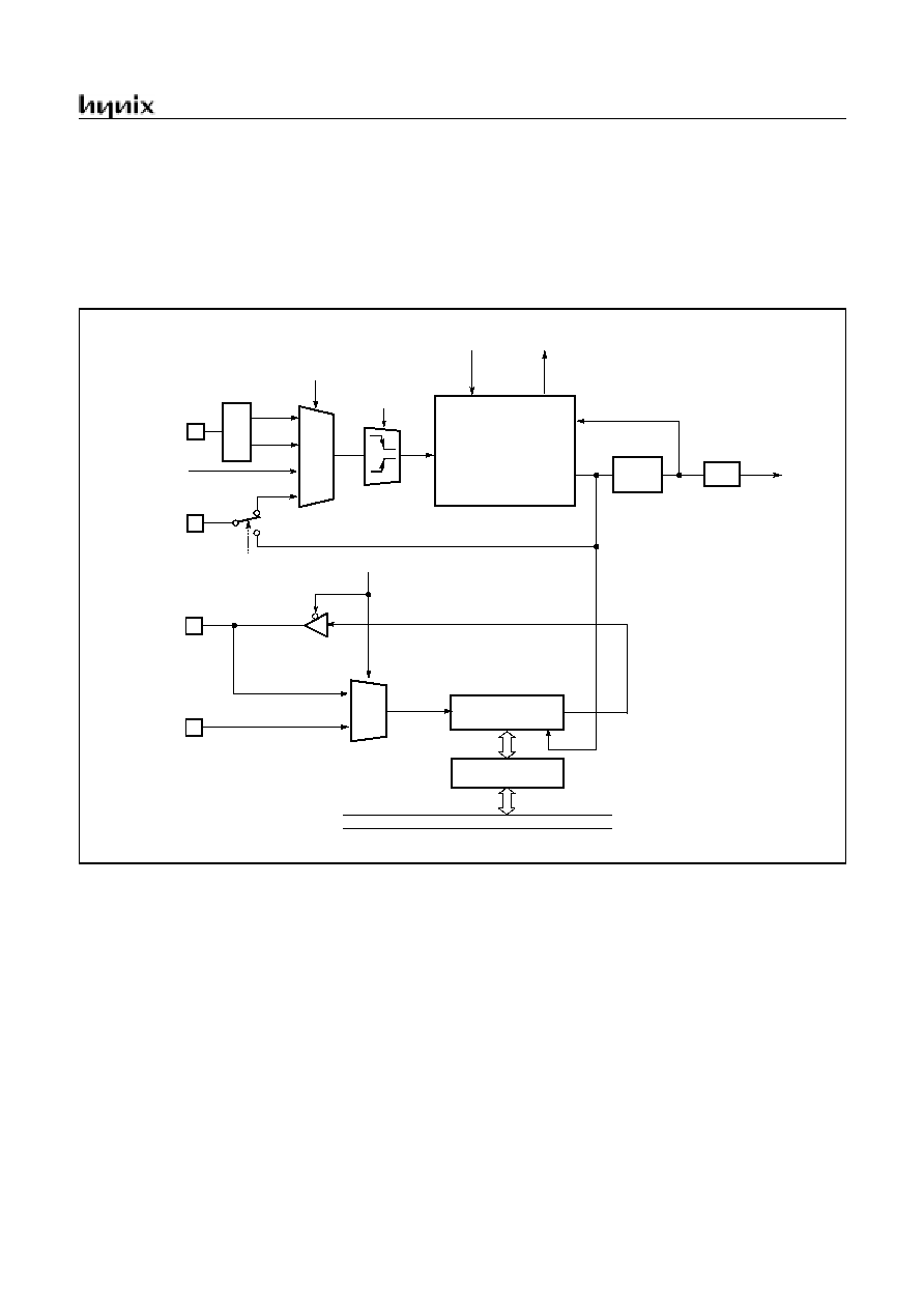
GMS81C2112/GMS81C2120
JUNE. 2001 Ver 1.00
59
14. SERIAL PERIPHERAL INTERFACE
The Serial Peripheral Interface (SPI) module is a serial in-
terface useful for communicating with other peripheral of
microcontroller devices. These peripheral devices may be
serial EEPROMs, shift registers, display drivers, A/D con-
verters, etc. The Serial Peripheral Interface(SPI) is 8-bit
clock synchronous type and consists of serial I/O register,
serial I/O mode register, clock selection circuit octal
counter and control circuit. The SOUT pin is designed to
input and output. So Serial Peripheral Interface(SPI) can
be operated with minimum two pin
Figure 14-1 SPI Block Diagram
÷
4
÷
16
XIN PIN
Pr
esca
ler
MUX
SCK[1:0]
00
01
10
11
SCLK PIN
SPI
Shift
Input shift register
SIOR
Clock
Clock
Octal
Serial communication
Interrupt
SIOIF
SOUT
Internal Bus
SIOSF
Counter
SCK[1:0]
"11"
overflow
not "11"
Complete
Timer0
Overflow
IOSWIN
SIN PIN
IOSW
PIN
SOUT
IOSWIN
CONTROL
CIRCUIT
"0"
"1"
POL
1
0
Start
SIOST
GMS81C2112/GMS81C2120
60
JUNE. 2001 Ver 1.00
Serial I/O Mode Register(SIOM) controls serial I/O func-
tion. According to SCK1 and SCK0, the internal clock or
external clock can be selected. The serial transmission op-
eration mode is decided by setting the SM1 and SM0, and
the polarity of transfer clock is selected by setting the POL.
Serial I/O Data Register(SIOR) is a 8-bit shift register.
First LSB is send or is received. When receiving mode, se-
rial input pin is selected by IOSW. The SPI allows 8-bits
of data to be synchronously transmitted and received.
To accomplish communication, typically three pins are
used:
- Serial Data In
R54/SIN
- Serial Data Out
R55/SOUT
- Serial Clock
R53/SCLK
.
Figure 14-2 SPI Control Register
BTCL
7
6
5
4
3
2
1
0
IOSW
POL
SIOST
Serial transmission status bit
Serial transmission Clock selection
INITIAL VALUE: 0000 0001
B
ADDRESS: 0E0
H
SIOM
SIOSF
Serial Input Pin Selection bit
0: SIN Pin Selection
1: IOSWIN Pin Selection
R/W
R/W
R/W
R/W
R/W
R
00: f
XIN
÷
4
01: f
XIN
÷
16
10: TMR0OV(Timer0 Overflow)
11: External Clock
0: Serial transmission is in progress
1: Serial transmission is completed
Serial transmission start bit
Setting this bit starts an Serial transmission.
After one cycle, bit is cleared to "0" by hardware.
SCK1 SCK0
SM1
SM0
R/W
Serial transmission Operation Mode
00: Normal Port(R55,R54,R53)
01: Sending Mode(SOUT,R54,SCLK)
10: Receiving Mode(R55,SIN,SCLK)
11: Sending & Receiving Mode(SOUT,SIN,SCLK)
INITIAL VALUE: Undefined
ADDRESS: 0E1
H
SIOR
BTCL
7
6
5
4
3
2
1
0
R/W R/W R/W R/W
R/W R/W
R/W
R/W
Sending Data at Sending Mode
Receiving Data at Receiving Mode
Serial Clock Polarity Selection bit
0: Data Transmission at Falling Edge
Received Data Latch at Rising Edge
1: Data Transmission at Rising Edge
Received Data Latch at Falling Edge
R/W
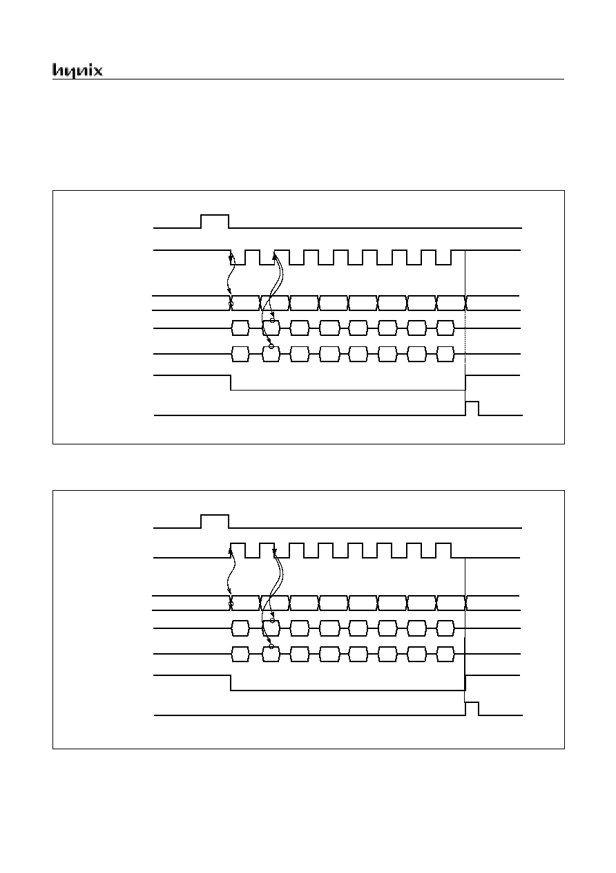
GMS81C2112/GMS81C2120
JUNE. 2001 Ver 1.00
61
14.1 Transmission/Receiving Timing
The serial transmission is started by setting SIOST(bit1 of
SIOM) to "1". After one cycle of SCK, SIOST is cleared
automatically to "0". The serial output data from 8-bit shift
register is output at falling edge of SCLK. And input data
is latched at rising edge of SCLK pin. When transmission
clock is counted 8 times, serial I/O counter is cleared as
`0". Transmission clock is halted in "H" state and serial I/
O interrupt(IFSIO) occurred.
Figure 14-3 SPI Timing Diagram at POL=0
Figure 14-4 SPI Timing Diagram at POL=1
D1
D2
D3
D4
D6
D7
D0
D5
D 1
D 2
D 3
D 4
D 6
D 7
D 0
D 5
SIOST
SCLK [R53]
(POL=0)
SOUT [R55]
SIN [R54]
SPIIF
(SPI Int. Req)
(IOSW=0)
D 1
D 2
D 3
D 4
D 6
D 7
D 0
D 5
IOSWIN [R55]
(IOSW=1)
SIOSF
(SPI Status)
D1
D2
D3
D4
D6
D7
D0
D5
D 1
D 2
D 3
D 4
D 6
D 7
D 0
D 5
SIOST
SCLK [R53]
(POL=1)
SOUT [R55]
SIN [R54]
SPIIF
(SPI Int. Req)
(IOSW=0)
D 1
D 2
D 3
D 4
D 6
D 7
D 0
D 5
IOSWIN [R55]
(IOSW=1)
SIOSF
(SPI Status)
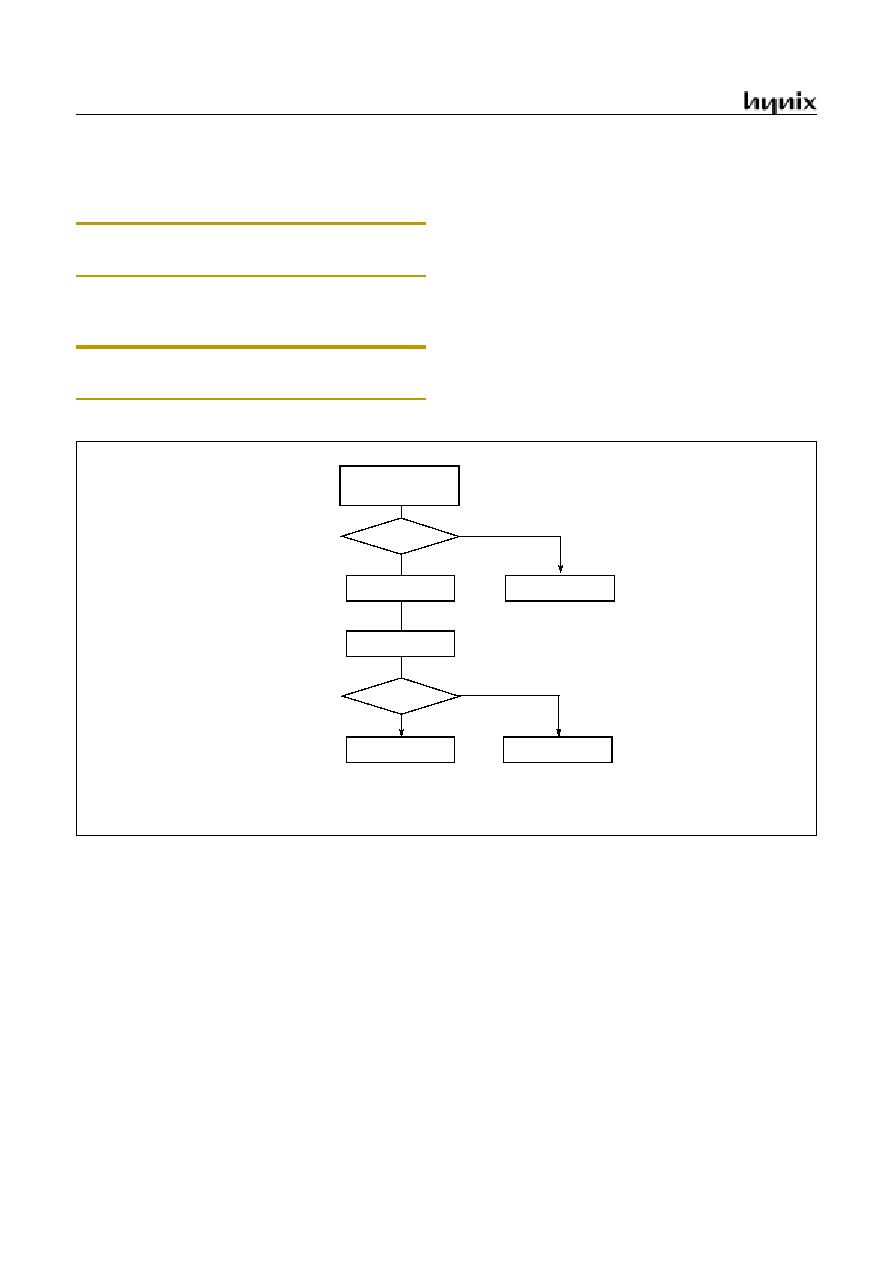
GMS81C2112/GMS81C2120
62
JUNE. 2001 Ver 1.00
14.2 The method of Serial I/O
Select transmission/receiving mode
Note: When external clock is used, the frequency should
be less than 1MHz and recommended duty is 50%.
In case of sending mode, write data to be send to SIOR.
Set SIOST to "1" to start serial transmission.
Note: If both transmission mode is selected and transmis-
sion is performed simultaneously it would be made error.
The SIO interrupt is generated at the completion of SIO
and SIOSF is set to "1". In SIO interrupt service routine,
correct transmission should be tested.
In case of receiving mode, the received data is acquired
by reading the SIOR.
14.3 The Method to Test Correct Transmission
Figure 14-5 Serial Method to Test Transmission
Serial I/O Interrupt
Service Routine
SE = 0
Write SIOM
Normal Operation
Overrun Error
Abnormal
SIOSF
0
1
- SE : Interrupt Enable Register Low IENL(Bit3)
- SR : Interrupt Request Flag Register Low IRQL(Bit3)
SR
0
1
GMS81C2112/GMS81C2120
JUNE. 2001 Ver 1.00
63
15. BUZZER FUNCTION
The buzzer driver block consists of 6-bit binary counter,
buzzer register BUR, and clock source selector. It gener-
ates square-wave which has very wide range frequency
(480Hz ~ 250kHz at f
XIN
= 4MHz) by user software.
A 50% duty pulse can be output to R03/BUZO pin to use
for piezo-electric buzzer drive
. Pin R03 is assigned for output
port of Buzzer driver by setting the bit 3 of R0FUNC(address
0F4
H
) to "1".
At this time, the pin R03 must be defined as
output mode (the bit 3 of R0IO=1).
Example: 5kHz output at 4MHz.
LDM
R0IO,#XXXX_1XXXB
LDM
BUR,#0011_0010B
LDM
R0FUNC,#XXXX_1XXXB
X means don't care
The bit 0 to 5 of BUR determines output frequency for
buzzer driving.
Equation of frequency calculation is shown below.
f
BUZ
: Buzzer frequency
f
XIN
: Oscillator frequency
Divide Ratio: Prescaler divide ratio by BUCK[1:0]
BUR: Lower 6-bit value of BUR. Buzzer period value.
The frequency of output signal is controlled by the buzzer
control register BUR.The bit 0 to bit 5 of BUR determine
output frequency for buzzer driving.
Figure 15-1 Block Diagram of Buzzer Driver
Figure 15-2 R0FUNC and Buzzer Register
f
BUZ
f
XIN
2
DivideRatio
BUR
1
+
(
)
×
×
----------------------------------------------------------------------------
=
Pres
caler
÷
8
÷
32
÷
16
÷
64
BUR
R03/BUZO PIN
R0FUNC
Internal bus line
R03 port data
XIN PIN
6-bit binary
2
6
[0DE
H
]
[0F4
H
]
0
1
F/F
÷
2
Comparator
Compare data
6-BIT COUNTER
MUX
00
01
10
11
Port selection
3
BUR[5:0]
BUR
ADDRESS: 0DE
H
RESET VALUE: Undefined
W
W
W
W
W
W
Source clock select
00:
÷
8
01:
÷
16
10:
÷
32
11:
÷
64
Buzzer Period Data
R03/BUZO Selection
R0FUNC
ADDRESS : 0F4
H
RESET VALUE : ---- 0000
B
W
-
-
0: R03 port (Turn off buzzer)
1: BUZO port (Turn on buzzer)
W
W
W
BUCK1 BUCK0
W
W
-
-
BUZO
EC0
INT1
INT0

GMS81C2112/GMS81C2120
64
JUNE. 2001 Ver 1.00
Note: BUR is undefined after reset, so it must be initialized
to between 1
H
and 3F
H
by software.
Note that BUR is a write-only register.
The 6-bit counter is cleared and starts the counting by writ-
ing signal at BUR register. It is incremental from 00
H
until
it matches 6-bit BUR value.
When main-frequency is 4MHz, buzzer frequency is
shown as below table.
BUR
[5:0]
BUR[7:6]
BUR
[5:0]
BUR[7:6]
00
01
10
11
00
01
10
11
00
01
02
03
04
05
06
07
250.000
125.000
83.333
62.500
50.000
41.667
35.714
31.250
125.000
62.500
41.667
31.250
25.000
20.833
17.857
15.625
62.500
31.250
20.833
15.625
12.500
10.417
8.929
7.813
31.250
15.625
10.417
7.813
6.250
5.208
4.464
3.906
20
21
22
23
24
25
26
27
7.576
7.353
7.143
6.944
6.757
6.579
6.410
6.250
3.788
3.676
3.571
3.472
3.378
3.289
3.205
3.125
1.894
1.838
1.786
1.736
1.689
1.645
1.603
1.563
0.947
0.919
0.893
0.868
0.845
0.822
0.801
0.781
08
09
0A
0B
0C
0D
0E
0F
27.778
25.000
22.727
20.833
19.231
17.857
16.667
15.625
13.889
12.500
11.364
10.417
9.615
8.929
8.333
7.813
6.944
6.250
5.682
5.208
4.808
4.464
4.167
3.906
3.472
3.125
2.841
2.604
2.404
2.232
2.083
1.953
28
29
2A
2B
2C
2D
2E
2F
6.098
5.952
5.814
5.682
5.556
5.435
5.319
5.208
3.049
2.976
2.907
2.841
2.778
2.717
2.660
2.604
1.524
1.488
1.453
1.420
1.389
1.359
1.330
1.302
0.762
0.744
0.727
0.710
0.694
0.679
0.665
0.651
10
11
12
13
14
15
16
17
14.706
13.889
13.158
12.500
11.905
11.364
10.870
10.417
7.353
6.944
6.579
6.250
5.952
5.682
5.435
5.208
3.676
3.472
3.289
3.125
2.976
2.841
2.717
2.604
1.838
1.736
1.645
1.563
1.488
1.420
1.359
1.302
30
31
32
33
34
35
36
37
5.102
5.000
4.902
4.808
4.717
4.630
4.545
4.464
2.551
2.500
2.451
2.404
2.358
2.315
2.273
2.232
1.276
1.250
1.225
1.202
1.179
1.157
1.136
1.116
0.638
0.625
0.613
0.601
0.590
0.579
0.568
0.558
18
19
1A
1B
1C
1D
1E
1F
10.000
9.615
9.259
8.929
8.621
8.333
8.065
7.813
5.000
4.808
4.630
4.464
4.310
4.167
4.032
3.906
2.500
2.404
2.315
2.232
2.155
2.083
2.016
1.953
1.250
1.202
1.157
1.116
1.078
1.042
1.008
0.977
38
39
3A
3B
3C
3D
3E
3F
4.386
4.310
4.237
4.167
4.098
4.032
3.968
3.907
2.193
2.155
2.119
2.083
2.049
2.016
1.984
1.953
1.096
1.078
1.059
1.042
1.025
1.008
0.992
0.977
0.548
0.539
0.530
0.521
0.512
0.504
0.496
0.488
GMS81C2112/GMS81C2120
JUNE. 2001 Ver 1.00
65
16. INTERRUPTS
The GMS81C21xx interrupt circuits consist of Interrupt
enable register (IENH, IENL), Interrupt request flags of
IRQH, IRQL, Priority circuit, and Master enable flag ("I"
flag of PSW). Nine interrupt sources are provided. The
configuration of interrupt circuit is shown in Figure 16-2.
The External Interrupts INT0 and INT1 each can be transi-
tion-activated (1-to-0 or 0-to-1 transition) by selection
IEDS.
The flags that actually generate these interrupts are bit
INT0F and INT1F in register IRQH. When an external in-
terrupt is generated, the flag that generated it is cleared by
the hardware when the service routine is vectored to only
if the interrupt was transition-activated.
The Timer 0 ~ Timer 1 Interrupts are generated by TxIF
which is set by a match in their respective timer/counter
register. The Basic Interval Timer Interrupt is generated by
BITIF which is set by an overflow in the timer register.
The AD converter Interrupt is generated by ADIF which is
set by finishing the analog to digital conversion.
The Watchdog timer Interrupt is generated by WDTIF
which set by a match in Watchdog timer register.
The Basic Interval Timer Interrupt is generated by BITIF
which are set by a overflow in the timer counter register.
The interrupts are controlled by the interrupt master enable
flag I-flag (bit 2 of PSW on page 21), the interrupt enable
register (IENH, IENL), and the interrupt request flags (in
IRQH and IRQL) except Power-on reset and software
BRK interrupt. Below table shows the Interrupt priority.
Vector addresses are shown in Figure 8-6 on page 23. In-
terrupt enable registers are shown in Figure 16-3. These
registers are composed of interrupt enable flags of each in-
terrupt source and these flags determines whether an inter-
rupt will be accepted or not. When enable flag is "0", a
corresponding interrupt source is prohibited. Note that
PSW contains also a master enable bit, I-flag, which dis-
ables all interrupts at once.
Figure 16-1 Interrupt Request Flag
Reset/Interrupt
Symbol
Priority
Hardware Reset
External Interrupt 0
External Interrupt 1
Timer/Counter 0
Timer/Counter 1
-
-
-
-
ADC Interrupt
Watchdog Timer
Basic Interval Timer
Serial Communication
RESET
INT0
INT1
TIMER0
TIMER1
-
-
-
-
ADC
WDT
BIT
SCI
-
1
2
3
4
-
-
-
-
5
6
7
8
R/W
INT0IF
INITIAL VALUE: 0000 ----
B
ADDRESS: 0E4
H
IRQH
INT1IF
MSB
T0IF
T1IF
R/W
Timer/Counter 1 interrupt request flag
SPIF
R/W
ADIF
Serial Communication interrupt request flag
INITIAL VALUE: 0000 ----
B
ADDRESS: 0E5
H
IRQL
WDTIF
MSB
LSB
-
-
-
BITIF
R/W
Timer/Counter 0 interrupt request flag
-
R/W
R/W
R/W
R/W
-
-
-
-
Basic Interval imer interrupt request flag
Watchdog timer interrupt request flag
A/D Conver interrupt request flag
External interrupt 1 request flag
External interrupt 0 request flag
LSB
-
-
-
-
-
-
-
-

GMS81C2112/GMS81C2120
66
JUNE. 2001 Ver 1.00
.
Figure 16-2 Block Diagram of Interrupt
Figure 16-3 Interrupt Enable Flag
Timer 0
INT1
INT0
INT0IF
IENH
Interrupt Enable
Interrupt Enable
IRQH
IRQL
Interrupt
Vector
Address
Generator
Internal bus line
Register (Lower byte)
Internal bus line
Register (Higher byte)
Release STOP
To CPU
Interrupt Master
Enable Flag
I-flag
IENL
Pr
io
r
i
ty
Co
n
t
r
o
l
I-flag is in PSW, it is cleared by "DI", set by
"EI" instruction. When it goes interrupt service,
I-flag is cleared by hardware, thus any other
interrupt are inhibited. When interrupt service is
completed by "RETI" instruction, I-flag is set to
"1" by hardware.
[0E2
H
]
[0E3
H
]
[0E4
H
]
[0E5
H
]
INT1IF
T0IF
Timer 1
T1IF
A/D Converter
ADIF
SIOIF
BITIF
Watchdog Timer
Serial
BIT
WDTIF
Communication
T1E
R/W
INT0E
INITIAL VALUE: 0000 ----
B
ADDRESS: 0E2
H
IENH
INT1E
MSB
T0E
R/W
Timer/Counter 1 interrupt enable flag
SPIE
R/W
ADE
Serial Communication interrupt enable flag
INITIAL VALUE: 0000 ----
B
ADDRESS: 0E3
H
IENL
WDTE
MSB
LSB
-
-
-
BITE
R/W
Timer/Counter 0 interrupt enable flag
-
R/W
R/W
R/W
R/W
-
-
-
-
Basic Interval imer interrupt enable flag
Watchdog timer interrupt enable flag
A/D Convert interrupt enable flag
External interrupt 1 enable flag
External interrupt 0 enable flag
0: Disable
1: Enable
VALUE
LSB
-
-
-
-
-
-
-
-
GMS81C2112/GMS81C2120
JUNE. 2001 Ver 1.00
67
16.1 Interrupt Sequence
An interrupt request is held until the interrupt is accepted
or the interrupt latch is cleared to "0" by a reset or an in-
struction. Interrupt acceptance sequence requires 8
f
XIN
(2
µ
s at f
MAIN
=4.19MHz) after the completion of the current
instruction execution. The interrupt service task is termi-
nated upon execution of an interrupt return instruction
[RETI].
Interrupt acceptance
1. The interrupt master enable flag (I-flag) is cleared to
"0" to temporarily disable the acceptance of any follow-
ing maskable interrupts. When a non-maskable inter-
rupt is accepted, the acceptance of any following
interrupts is temporarily disabled.
2. Interrupt request flag for the interrupt source accepted is
cleared to "0".
3. The contents of the program counter (return address)
and the program status word are saved (pushed) onto the
stack area. The stack pointer decreases 3 times.
4. The entry address of the interrupt service program is
read from the vector table address and the entry address
is loaded to the program counter.
5. The instruction stored at the entry address of the inter-
rupt service program is executed.
Figure 16-4 Timing chart of Interrupt Acceptance and Interrupt Return Instruction
A interrupt request is not accepted until the I-flag is set to
"1" even if a requested interrupt has higher priority than
that of the current interrupt being serviced.
When nested interrupt service is required, the I-flag should
be set to "1" by "EI" instruction in the interrupt service
program. In this case, acceptable interrupt sources are se-
lectively enabled by the individual interrupt enable flags.
Saving/Restoring General-purpose Register
During interrupt acceptance processing, the program
counter and the program status word are automatically
saved on the stack, but accumulator and other registers are
not saved itself. These registers are saved by the software
if necessary. Also, when multiple interrupt services are
nested, it is necessary to avoid using the same data memory
V.L.
System clock
Address Bus
PC
SP
SP-1
SP-2
V.H.
New PC
V.L.
Data Bus
Not used
PCH
PCL
PSW
ADL
OP code
ADH
Instruction Fetch
Internal Read
Internal Write
Interrupt Processing Step
Interrupt Service Task
V.L. and V.H. are vector addresses.
ADL and ADH are start addresses of interrupt service routine as vector contents.
Basic Interval Timer
012
H
0E3
H
0FFE6
H
0FFE7
H
0E
H
2E
H
0E312
H
0E313
H
Entry Address
Correspondence between vector table address for BIT interrupt
and the entry address of the interrupt service program.
Vector Table Address
GMS81C2112/GMS81C2120
68
JUNE. 2001 Ver 1.00
area for saving registers.
The following method is used to save/restore the general-
purpose registers.
Example: Register save using push and pop instructions
General-purpose register save/restore using push and pop
instructions;
16.2 BRK Interrupt
Software interrupt can be invoked by BRK instruction,
which has the lowest priority order.
Interrupt vector address of BRK is shared with the vector
of TCALL 0 (Refer to Program Memory Section). When
BRK interrupt is generated, B-flag of PSW is set to distin-
guish BRK from TCALL 0.
Each processing step is determined by B-flag as shown in
Figure 16-5.
Figure 16-5 Execution of BRK/TCALL0
INTxx:
PUSH
A
PUSH
X
PUSH
Y
;SAVE ACC.
;SAVE X REG.
;SAVE Y REG.
interrupt processing
POP
Y
POP
X
POP
A
RETI
;RESTORE Y REG.
;RESTORE X REG.
;RESTORE ACC.
;RETURN
main task
interrupt
service task
saving
registers
restoring
registers
acceptance of
interrupt
interrupt return
B-FLAG
BRK
INTERRUPT
ROUTINE
RETI
TCALL0
ROUTINE
RET
BRK or
TCALL0
=0
=1

GMS81C2112/GMS81C2120
JUNE. 2001 Ver 1.00
69
16.3 Multi Interrupt
If two requests of different priority levels are received si-
multaneously, the request of higher priority level is ser-
viced. If requests of the interrupt are received at the same
time simultaneously, an internal polling sequence deter-
mines by hardware which request is serviced.
Figure 16-6 Execution of Multi Interrupt
However, multiple processing through software for special
features is possible. Generally when an interrupt is accept-
ed, the I-flag is cleared to disable any further interrupt. But
as user sets I-flag in interrupt routine, some further inter-
rupt can be serviced even if certain interrupt is in progress.
Example: During Timer1 interrupt is in progress, INT0 in-
terrupt serviced without any suspend.
TIMER1:
PUSH
A
PUSH
X
PUSH
Y
LDM
IENH,#80H
;
Enable INT0 only
LDM
IENL,#0
;
Disable other
EI
;
Enable Interrupt
:
:
:
:
:
:
LDM
IENH,#0F0H
;
Enable all interrupts
LDM
IENL,#0F0H
POP
Y
POP
X
POP
A
RETI
enable INT0
TIMER 1
service
INT0
service
Main Program
service
Occur
TIMER1 interrupt
Occur
INT0
EI
disable other
enable INT0
enable other
In this example, the INT0 interrupt can be serviced without any
pending, even TIMER1 is in progress.
Because of re-setting the interrupt enable registers IENH,IENL
and master enable "EI" in the TIMER1 routine.

GMS81C2112/GMS81C2120
70
JUNE. 2001 Ver 1.00
16.4 External Interrupt
The external interrupt on INT0 and INT1 pins are edge
triggered depending on the edge selection register IEDS
(address 0F8
H
) as shown in Figure 16-7.
The edge detection of external interrupt has three transition
activated mode: rising edge, falling edge, and both edge.
Figure 16-7 External Interrupt Block Diagram
INT0 and INT1 are multiplexed with general I/O ports
(R00 and R01). To use as an external interrupt pin, the bit
of R4 port mode register R0FUNC should be set to "1" cor-
respondingly.
Example: To use as an INT0 and INT1
:
:
;
**** Set port as an input port R00,R01
LDM
R0IO,#1111_1100B
;
;
**** Set port as an interrupt port
LDM
R0FUNC,#0000_0011B
;
;
**** Set Falling-edge Detection
LDM
IEDS,#0000_0101B
:
:
:
Response Time
The INT0 and INT1 edge are latched into INT0IF and
INT1IF at every machine cycle. The values are not actually
polled by the circuitry until the next machine cycle. If a re-
quest is active and conditions are right for it to be acknowl-
edged, a hardware subroutine call to the requested service
routine will be the next instruction to be executed. The
DIV itself takes twelve cycles. Thus, a minimum of twelve
complete machine cycles elapse between activation of an
external interrupt request and the beginning of execution
of the first instruction of the service routine.
Figure 16-8shows interrupt response timings.
Figure 16-8 Interrupt Response Timing Diagram
INT1IF
INT1 pin
INT1 INTERRUPT
IEDS
[0E6H]
INT0IF
INT0 pin
INT0 INTERRUPT
Edge selection
Register
2
2
Interrupt
goes
active
Interrupt
latched
Interrupt
processing
Interrupt
routine
8 f
XIN
max. 12 f
XIN
GMS81C2112/GMS81C2120
JUNE. 2001 Ver 1.00
71
Figure 16-9 R0FUNC and IEDS Registers
BTCL
W
W
W
W
W
W
W
W
-
-
-
INT1
0: R00
1: INT0
INITIAL VALUE: ---- 0000
B
ADDRESS: 0F4
H
R0FUNC
-
INT0
EC0
BUZO
0: R01
1: INT1
0: R02
1: EC0
0: R03
1: BUZO
LSB
MSB
BTCL
R/W
R/W
R/W
R/W
-
-
-
IED0H
INITIAL VALUE: ---- 0000
B
ADDRESS: 0E6
H
IEDS
-
IED0L
IED1L
IED1H
LSB
MSB
Edge selection register
00: Reserved
01: Falling (1-to-0 transition)
10: Rising (0-to-1 transition)
11: Both (Rising & Falling)
INT0
INT1
GMS81C2112/GMS81C2120
72
JUNE. 2001 Ver 1.00
17. Power Saving Mode
For applications where power consumption is a critical
factor, device provides four kinds of power saving func-
tions, STOP mode, Sub-active mode and Wake-up Timer
mode (Stand-by mode, Watch mode). Table 17-1 shows
the status of each Power Saving Mode.
The power saving function is activated by execution of
STOP instruction and by execution of STOP instruction af-
ter setting the corresponding status (WAKEUP) of
CKCTLR. We shows the release sources from each Power
Saving Mode
Peripheral
STOP Mode
Wake-up Timer
Mode
Stand-by Mode
RAM
Retain
Retain
Control Registers
Retain
Retain
I/O Ports
Retain
Retain
CPU
Stop
Stop
Timer0
Stop
Operation
Oscillation
Stop
Oscillation
Prescaler
Stop
÷
2048 only
Entering Condition
[WAKEUP]
0
1
Table 17-1 Power Saving Mode
Release Source
STOP Mode
Wake-up Timer
Mode
Stand-by Mode
RESET
O
O
RCWDT
O
O
EXT.INT0
O
O
EXT.INT1
Timer0
X
O
Table 17-2 Release Sources from Power Saving Mode
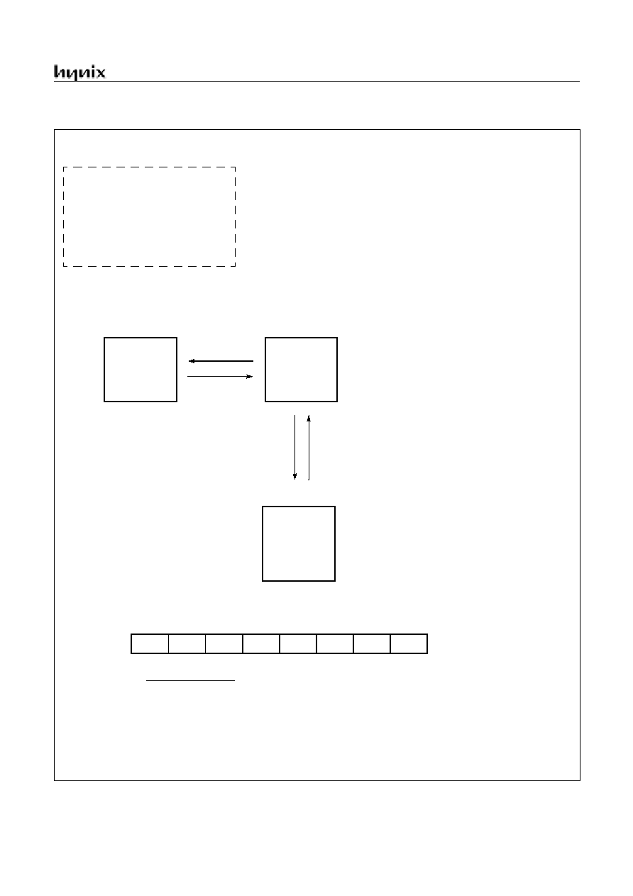
GMS81C2112/GMS81C2120
JUNE. 2001 Ver 1.00
73
17.1 Operating Mode
ACTIVE Mode
f
XI
: oscillation
cpu : f
SYS
tmr : f
SYS
peri : f
SYS
STANDBY Mode
f
XI
: oscillation
cpu : stop
tmr : ps11(f
XI
)
peri : stop
CKCTLR[10]
+
STOP
TIMER0
EXT_INT
RESET
RC_WDT
STOP Mode
f
XI
: stop
cpu : stop
tmr : stop
peri : stop
EXT_INT
RESET
RC_WDT
CKCTLR[00]
+
STOP
System Clock Mode Register
SCMR
ADDRESS : FAH
RESET VALUE : ---00---
-
-
-
CS1
CS0
-
-
-
CS[1:0]
Clock selection enable bits
00 : f
XI
10 : f
XI
÷
8
01 : f
XI
÷
4 11 : f
XI
÷
32
f
SYS
: f
XI
,f
XI
÷4
,f
XI
÷
8,f
XI
÷
32
cpu : system clock
tmr : timer0 clock
peri : peripheral clock
CKCTLR = CKCTLR[6:5]
f
XI
: Main clock frequency
GMS81C2112/GMS81C2120
74
JUNE. 2001 Ver 1.00
17.2 Stop Mode
In the Stop mode, the on-chip oscillator is stopped. With
the clock frozen, all functions are stopped, but the on-chip
RAM and Control registers are held. The port pins out the
values held by their respective port data register, port di-
rection registers. Oscillator stops and the systems internal
operations are all held up.
· The states of the RAM, registers, and latches valid
immediately before the system is put in the STOP
state are all held.
· The program counter stop the address of the
instruction to be executed after the instruction
"STOP" which starts the STOP operating mode.
The Stop mode is activated by execution of STOP in-
struction after clearing the bit WAKEUP of CKCTLR
to "0". (This register should be written by byte opera-
tion. If this register is set by bit manipulation instruc-
tion, for example "set1" or "clr1" instruction, it may
be undesired operation)
In the Stop mode of operation, V
DD
can be reduced to min-
imize power consumption. Care must be taken, however,
to ensure that V
DD
is not reduced before the Stop mode is
invoked, and that V
DD
is restored to its normal operating
level, before the Stop mode is terminated.
The reset should not be activated before V
DD
is restored to
its normal operating level, and must be held active long
enough to allow the oscillator to restart and stabilize.
Note: After STOP instruction, at least two or more NOP in-
struction should be written
Ex)
LDM CKCTLR,#0000_1110B
STOP
NOP
NOP
In the STOP operation, the dissipation of the power asso-
ciated with the oscillator and the internal hardware is low-
ered; however, the power dissipation associated with the
pin interface (depending on the external circuitry and pro-
gram) is not directly determined by the hardware operation
of the STOP feature. This point should be little current
flows when the input level is stable at the power voltage
level (V
DD
/V
SS
); however, when the input level gets high-
er than the power voltage level (by approximately 0.3 to
0.5V), a current begins to flow. Therefore, if cutting off the
output transistor at an I/O port puts the pin signal into the
high-impedance state, a current flow across the ports input
transistor, requiring to fix the level by pull-up or other
means.
Release the STOP mode
The exit from STOP mode is hardware reset or external in-
terrupt. Reset re-defines all the Control registers but does
not change the on-chip RAM. External interrupts allow
both on-chip RAM and Control registers to retain their val-
ues.
If I-flag = 1, the normal interrupt response takes place. If I-
flag = 0, the chip will resume execution starting with the
instruction following the STOP instruction. It will not vec-
tor to interrupt service routine. (refer to Figure 17-1)
When exit from Stop mode by external interrupt, enough
oscillation stabilization time is required to normal opera-
tion. Figure 17-2 shows the timing diagram. When release
the Stop mode, the Basic interval timer is activated on
wake-up. It is increased from 00
H
until FF
H
. The count
overflow is set to start normal operation. Therefore, before
STOP instruction, user must be set its relevant prescaler di-
vide ratio to have long enough time (more than 20msec).
This guarantees that oscillator has started and stabilized.
By reset, exit from Stop mode is shown in Figure .
Figure 17-1 STOP Releasing Flow by Interrupts
IEXX
=0
=1
STOP
INSTRUCTION
STOP Mode
Interrupt Request
STOP Mode Release
I-FLAG
=1
Interrupt Service Routine
Next
INSTRUCTION
=0
Master Interrupt
Enable Bit PSW[2]
Corresponding Interrupt
Enable Bit (IENH, IENL)
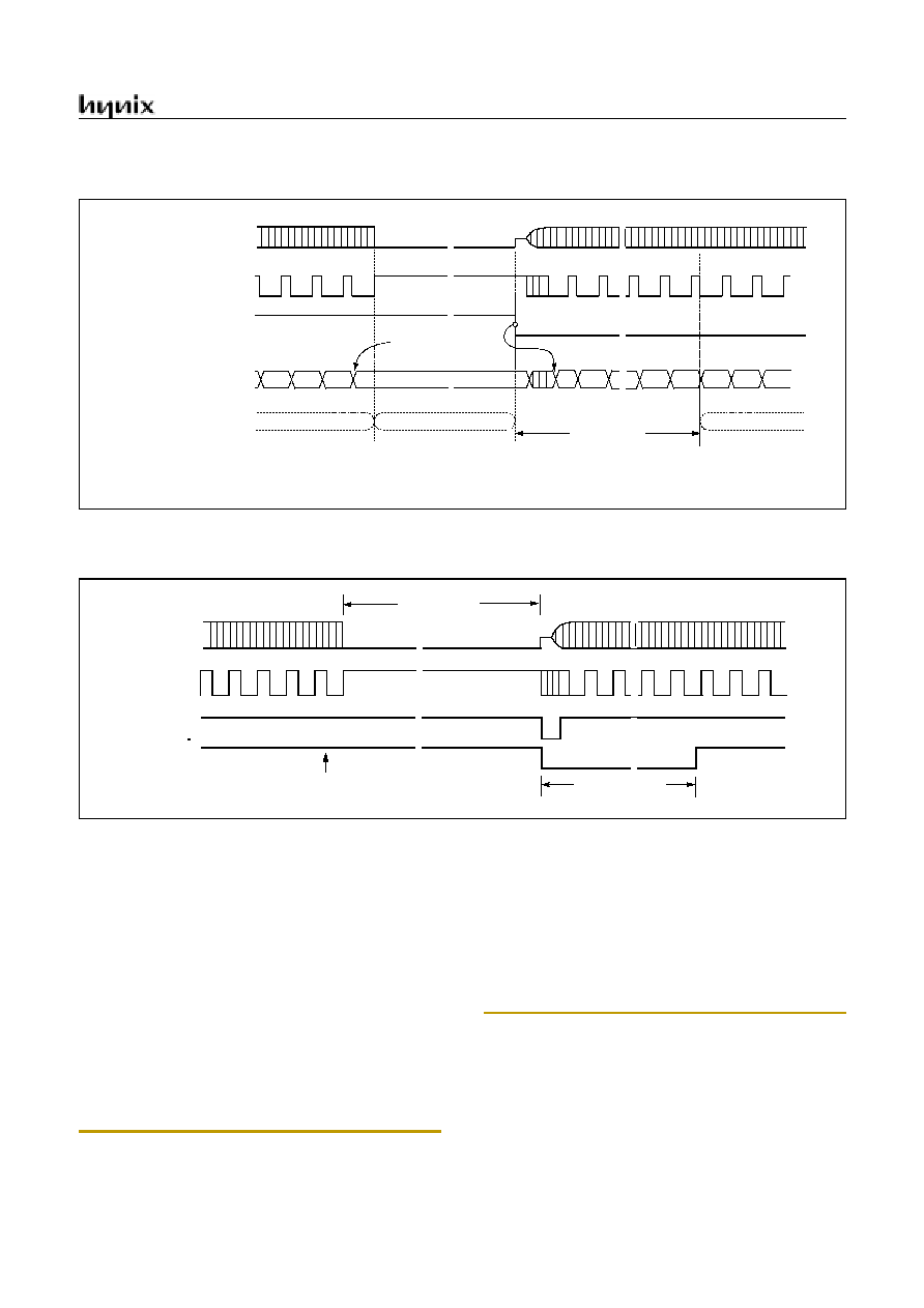
GMS81C2112/GMS81C2120
JUNE. 2001 Ver 1.00
75
.
Figure 17-2 STOP Mode Release Timing by External Interrupt
Figure 17-3 Timing of STOP Mode Release by RESET
17.3 Wake-up Timer Mode
In the Wake-up Timer mode, the on-chip oscillator is not
stopped. Except the Prescaler(only 2048 divided ratio) and
Timer0, all functions are stopped, but the on-chip RAM
and Control registers are held. The port pins out the values
held by their respective port data register, port direction
registers.
The Wake-up Timer mode is activated by execution of
STOP instruction after setting the bit WAKEUP of
CKCTLR to "1". (This register should be written by
byte operation. If this register is set by bit manipulation
instruction, for example "set1" or "clr1" instruction, it
may be undesired operation)
Note: After STOP instruction, at least two or more NOP in-
struction should be written
Ex)
LDM TDR0,#0FFH
LDM TM0,#0001_1011B
LDM CKCTLR,#0100_1110B
STOP
NOP
NOP
In addition, the clock source of timer0 should be selected
to 2048 divided ratio. Otherwise, the wake-up function can
not work. And the timer0 can be operated as 16-bit timer
with timer1. (refer to timer function)The period of wake-
up function is varied by setting the timer data register 0,
TDR0.
Before executing Stop instruction, Basic Interval Timer must be set
Oscillator
(X
IN
pin)
~~
n
0
BIT Counter
n+1
n+2
n+3
~~
Normal Operation
Stop Operation
Normal Operation
1
FE
FF
0
1
2
~~
~~
~~
t
ST
>
20ms
~~
~~
External Interrupt
Internal Clock
Clear
STOP Instruction
Executed
~~
~~
~~
properly by software to get stabilization time which is longer than 20ms.
by software
~~
~~
STOP Mode
Time can not be control by software
Oscillator
(XI pin)
~~
~~
~~
STOP Instruction Execution
Stabilization Time
t
ST
= 64mS @4MHz
Internal
Clock
Internal
~~
~~
~~
~~
~~
RESETB
RESETB
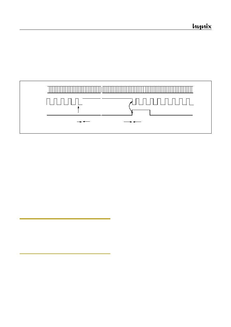
GMS81C2112/GMS81C2120
76
JUNE. 2001 Ver 1.00
Release the Wake-up Timer mode
The exit from Wake-up Timer mode is hardware reset,
Timer0 overflow or external interrupt. Reset re-defines all
the Control registers but does not change the on-chip
RAM. External interrupts and Timer0 overflow allow both
on-chip RAM and Control registers to retain their values.
If I-flag = 1, the normal interrupt response takes place. If I-
flag = 0, the chip will resume execution starting with the
instruction following the STOP instruction. It will not vec-
tor to interrupt service routine.(refer to Figure 17-1)
When exit from Wake-up Timer mode by external inter-
rupt or timer0 overflow, the oscillation stabilization time is
not required to normal operation. Because this mode do not
stop the on-chip oscillator shown as Figure 17-4.
Figure 17-4 Wake-up Timer Mode Releasing by External Interrupt or Timer0 Interrupt
17.4 Internal RC-Oscillated Watchdog Timer Mode
In the Internal RC-Oscillated Watchdog Timer mode, the
on-chip oscillator is stopped. But internal RC oscillation
circuit is oscillated in this mode. The on-chip RAM and
Control registers are held. The port pins out the values held
by their respective port data register, port direction regis-
ters.
The Internal RC-Oscillated Watchdog Timer mode is
activated by execution of STOP instruction after set-
ting the bit WAKEUP and RCWDT of CKCTLR to "
01 ". (This register should be written by byte operation.
If this register is set by bit manipulation instruction, for
example "set1" or "clr1" instruction, it may be unde-
sired operation)
Note: Caution: After STOP instruction, at least two or more
NOP instruction should be written
Ex)
LDM WDTR,#1111_1111B
LDM CKCTLR,#0010_1110B
STOP
NOP
NOP
The exit from Internal RC-Oscillated Watchdog Timer
mode is hardware reset or external interrupt. Reset re-de-
fines all the Control registers but does not change the on-
chip RAM. External interrupts allow both on-chip RAM
and Control registers to retain their values.
If I-flag = 1, the normal interrupt response takes place. In
this case, if the bit WDTON of CKCTLR is set to "0" and
the bit WDTE of IENH is set to "1", the device will execute
the watchdog timer interrupt service routine.(Figure 17-5)
However, if the bit WDTON of CKCTLR is set to "1", the
device will generate the internal RESET signal and exe-
cute the reset processing. (Figure 17-6)
If I-flag = 0, the chip will resume execution starting with
the instruction following the STOP instruction. It will not
vector to interrupt service routine.(refer to Figure 17-1)
When exit from Internal RC-Oscillated Watchdog Timer
mode by external interrupt, the oscillation stabilization
time is required to normal operation. Figure 17-5 shows
the timing diagram. When release the Internal RC-Oscil-
lated Watchdog Timer mode, the basic interval timer is ac-
tivated on wake-up. It is increased from 00
H
until FF
H
. The
count overflow is set to start normal operation. Therefore,
before STOP instruction, user must be set its relevant pres-
caler divide ratio to have long enough time (more than
20msec). This guarantees that oscillator has started and
stabilized.
By reset, exit from internal RC-Oscillated Watchdog Tim-
er mode is shown in Figure 17-6.
Wake-up Timer Mode
Oscillator
(XI pin)
~~
STOP Instruction
Normal Operation
Normal Operation
CPU
Clock
Request
Interrupt
~~
~~
Execution
Do not need Stabilization Time
( stop the CPU clock )
~~
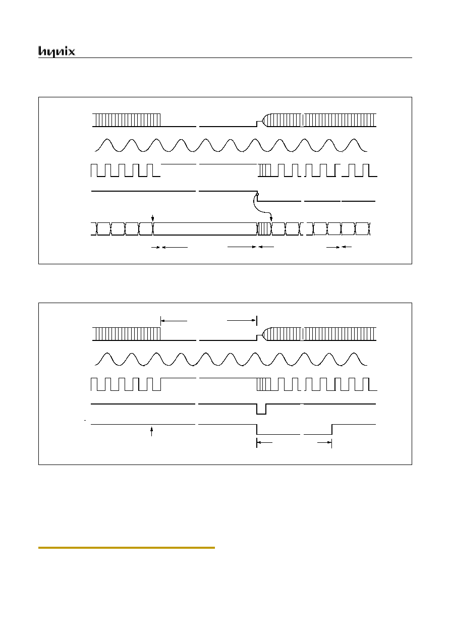
GMS81C2112/GMS81C2120
JUNE. 2001 Ver 1.00
77
Figure 17-5 Internal RCWDT Mode Releasing by External Interrupt or WDT Interrupt
Figure 17-6 Internal RCWDT Mode Releasing by RESET
17.5 Minimizing Current Consumption
The Stop mode is designed to reduce power consumption.
To minimize current drawn during Stop mode, the user
should turn-off output drivers that are sourcing or sinking
current, if it is practical.
Note: In the STOP operation, the power dissipation asso-
ciated with the oscillator and the internal hardware is low-
ered; however, the power dissipation associated with the
pin interface (depending on the external circuitry and pro-
gram) is not directly determined by the hardware operation
of the STOP feature. This point should be little current flows
when the input level is stable at the power voltage level
(V
DD
/V
SS
); however, when the input level becomes higher
~~
RCWDT Mode
Normal Operation
Oscillator
(XI pin)
~~
~~
N+1
N
N+2
00
01
FE
FF
00
00
N-1
N-2
~~
~~
~~
~~
~~
Clear Basic Interval Timer
STOP Instruction Execution
Normal Operation
Stabilization Time
t
ST
> 20mS
Internal
Clock
External
Interrupt
BIT
Counter
~~
Internal
RC Clock
( or WDT Interrupt )
~~
Oscillator
(XI pin)
~~
~~
~~
~~
Internal
Clock
Internal
RC Clock
Time can not be control by software
~~
STOP Instruction Execution
Stabilization Time
t
ST
= 64mS @4MHz
Internal
~~
~~
~~
RESET by WDT
RESET
RESET
RCWDT Mode
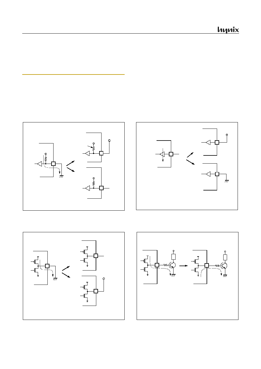
GMS81C2112/GMS81C2120
78
JUNE. 2001 Ver 1.00
than the power voltage level (by approximately 0.3V), a cur-
rent begins to flow. Therefore, if cutting off the output tran-
sistor at an I/O port puts the pin signal into the high-
impedance state, a current flow across the ports input tran-
sistor, requiring it to fix the level by pull-up or other means.
It should be set properly in order that current flow through
port doesn't exist.
First conseider the setting to input mode. Be sure that there
is no current flow after considering its relationship with
external circuit. In input mode, the pin impedance viewing
from external MCU is very high that the current doesn't
flow.
But input voltage level should be V
SS
or V
DD
. Be careful
that if unspecified voltage, i.e. if unfirmed voltage level
(not V
SS
or V
DD
) is applied to input pin, there can be little
current (max. 1mA at around 2V) flow.
If it is not appropriate to set as an input mode, then set to
output mode considering there is no current flow. Setting
to High or Low is decided considering its relationship with
external circuit. For example, if there is external pull-up re-
sistor then it is set to output mode, i.e. to High, and if there
is external pull-down register, it is set to low.
Figure 17-7 Application Example of Unused Input Port
Figure 17-8 Application Example of Unused Output Port
INPUT PIN
V
DD
GND
i
V
DD
X
Weak pull-up current flows
V
DD
internal
pull-up
INPUT PIN
i
V
DD
X
Very weak current flows
V
DD
O
O
OPEN
OPEN
i=0
O
i=0
O
GND
When port is configured as an input, input level should
be closed to 0V or 5V to avoid power consumption.
OUTPUT PIN
GND
i
In the left case, much current flows from port to GND.
X
ON
OFF
OUTPUT PIN
GND
i
In the left case, Tr. base current flows from port to GND.
i=0
X
OFF
ON
V
DD
L
ON
OFF
OPEN
GND
V
DD
L
ON
OFF
To avoid power consumption, there should be low output
ON
OFF
O
O
V
DD
O
to the port .
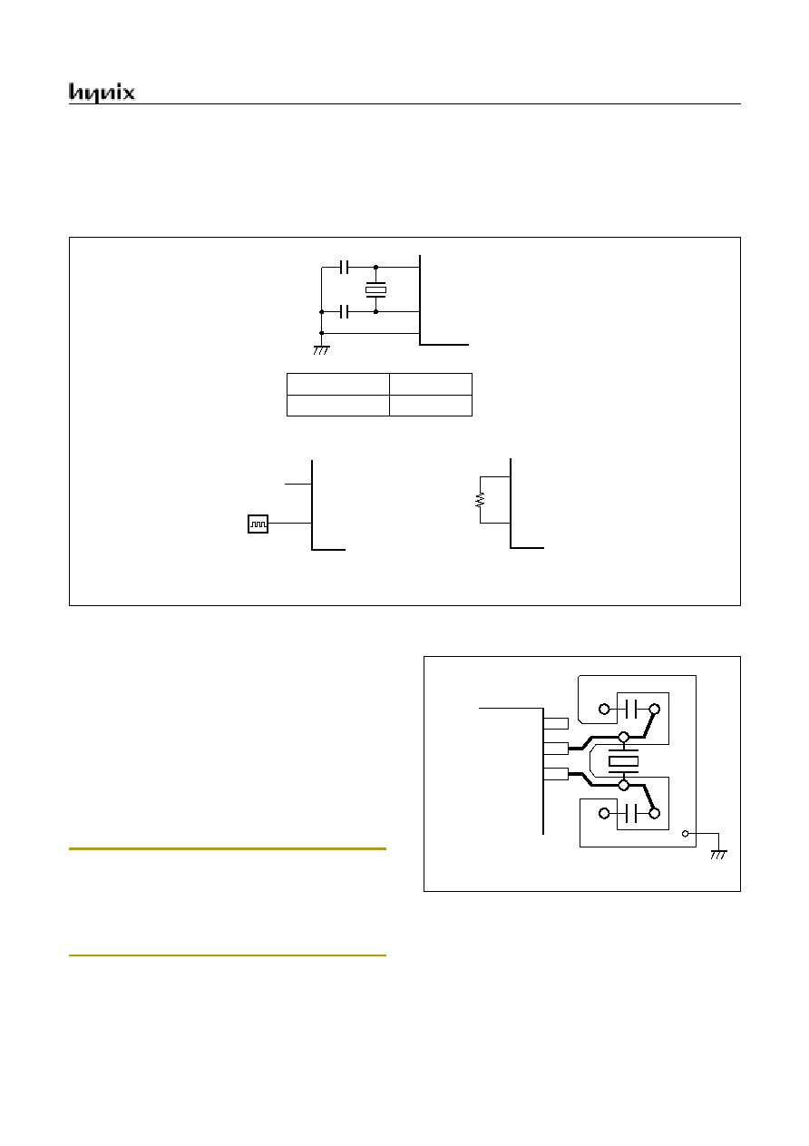
GMS81C2112/GMS81C2120
JUNE. 2001 Ver 1.00
79
18. OSCILLATOR CIRCUIT
The GMS81C21xx has an oscillation circuits internally.
X
IN
and X
OUT
are input and output for main frequency re-
spectively, inverting amplifier which can be configured for
being used as an on-chip oscillator, as shown in Figure 18-
1.
Figure 18-1 Oscillation Circuit
Oscillation circuit is designed to be used either with a ce-
ramic resonator or crystal oscillator. Since each crystal and
ceramic resonator have their own characteristics, the user
should consult the crystal manufacturer for appropriate
values of external components.
Oscillation circuit is designed to be used either with a ce-
ramic resonator or crystal oscillator. Since each crystal and
ceramic resonator have their own characteristics, the user
should consult the crystal manufacturer for appropriate
values of external components.
In addition, see Figure 18-2 for the layout of the crystal.
Note: Minimize the wiring length. Do not allow the wiring to
intersect with other signal conductors. Do not allow the wir-
ing to come near changing high current. Set the potential of
the grounding position of the oscillator capacitor to that of
V
SS
. Do not ground it to any ground pattern where high cur-
rent is present. Do not fetch signals from the oscillator.
Figure 18-2 Layout of Oscillator PCB circuit
X
OUT
X
IN
V
SS
Recommend
C1,C2 = 20pF
C1
C2
X
OUT
X
IN
External Clock
Open
X
OUT
X
IN
External Oscillator
RC Oscillator (mask option)
Crystal or Ceramic Oscillator
4.19MHz
Crystal Oscillator
Ceramic Resonator
C1,C2 = 30pF
Refer to AC Characteristics
For selection R value,
R
EXT
X
OUT
X
IN
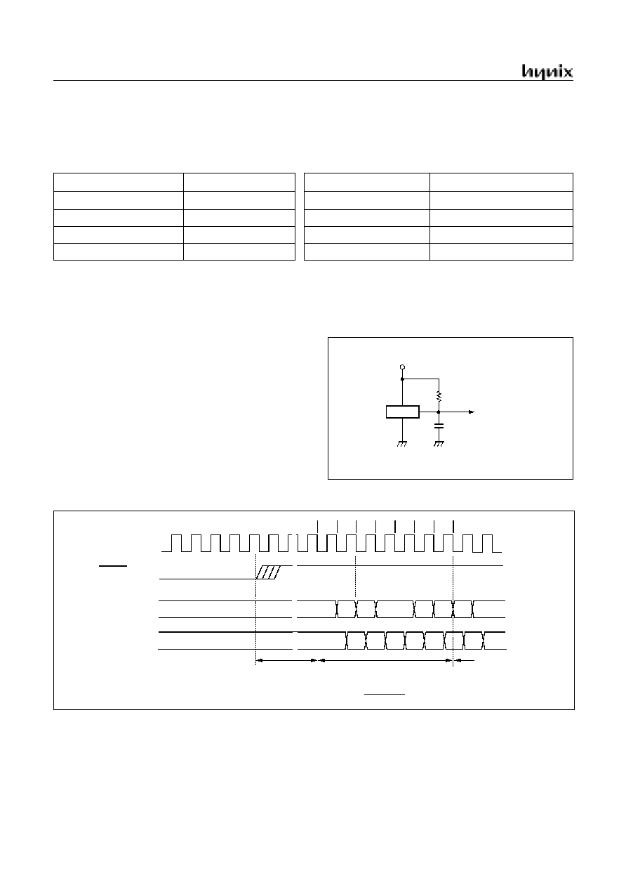
GMS81C2112/GMS81C2120
80
JUNE. 2001 Ver 1.00
19. RESET
The GMS81C21xx have two types of reset generation pro-
cedures; one is an external reset input, the other is a watch-
dog timer reset. Table 19-1 shows on-chip hardware ini-
tialization by reset action.
Table 19-1 Initializing Internal Status by Reset Action
19.1 External Reset Input
The reset input is the RESET pin, which is the input to a
Schmitt Trigger. A reset in accomplished by holding the
RESET pin low for at least 8 oscillator periods, within the
operating voltage range and oscillation stable, it is applied,
and the internal state is initialized. After reset, 64ms (at 4
MHz) add with 7 oscillator periods are required to start ex-
ecution as shown in Figure 19-2.
Internal RAM is not affected by reset. When V
DD
is turned
on, the RAM content is indeterminate. Therefore, this
RAM should be initialized before read or tested it.
When the RESET pin input goes to high, the reset opera-
tion is released and the program execution starts at the vec-
tor address stored at addresses FFFE
H
- FFFF
H
.
A connection for simple power-on-reset is shown in Figure
19-1.
Figure 19-1 Simple Power-on-Reset Circuit
Figure 19-2 Timing Diagram after RESET
19.2 Watchdog Timer Reset
Refer to "11. WATCHDOG TIMER" on page 39.
On-chip Hardware
Initial Value
On-chip Hardware
Initial Value
Program counter
(PC)
(FFFF
H
) - (FFFE
H
)
Peripheral clock
Off
RAM page register
(RPR)
0
Watchdog timer
Disable
G-flag
(G)
0
Control registers
Refer to Table 8-1 on page 27
Operation mode
Main-frequency clock
Power fail detector
Disable
7036P
V
CC
10uF
+
10k
to the RESET pin
MAIN PROGRAM
Oscillator
(X
IN
pin)
?
?
FFFE FFFF
Stabilization Time
t
ST
= 62.5mS at 4.19MHz
RESET
ADDRESS
DATA
1
2
3
4
5
6
7
?
?
Start
?
?
?
FE
?
ADL
ADH
OP
BUS
BUS
RESET Process Step
~~
~~
~~
~~
~~
~~
t
ST
=
x 256
f
MAIN
÷
1024
1
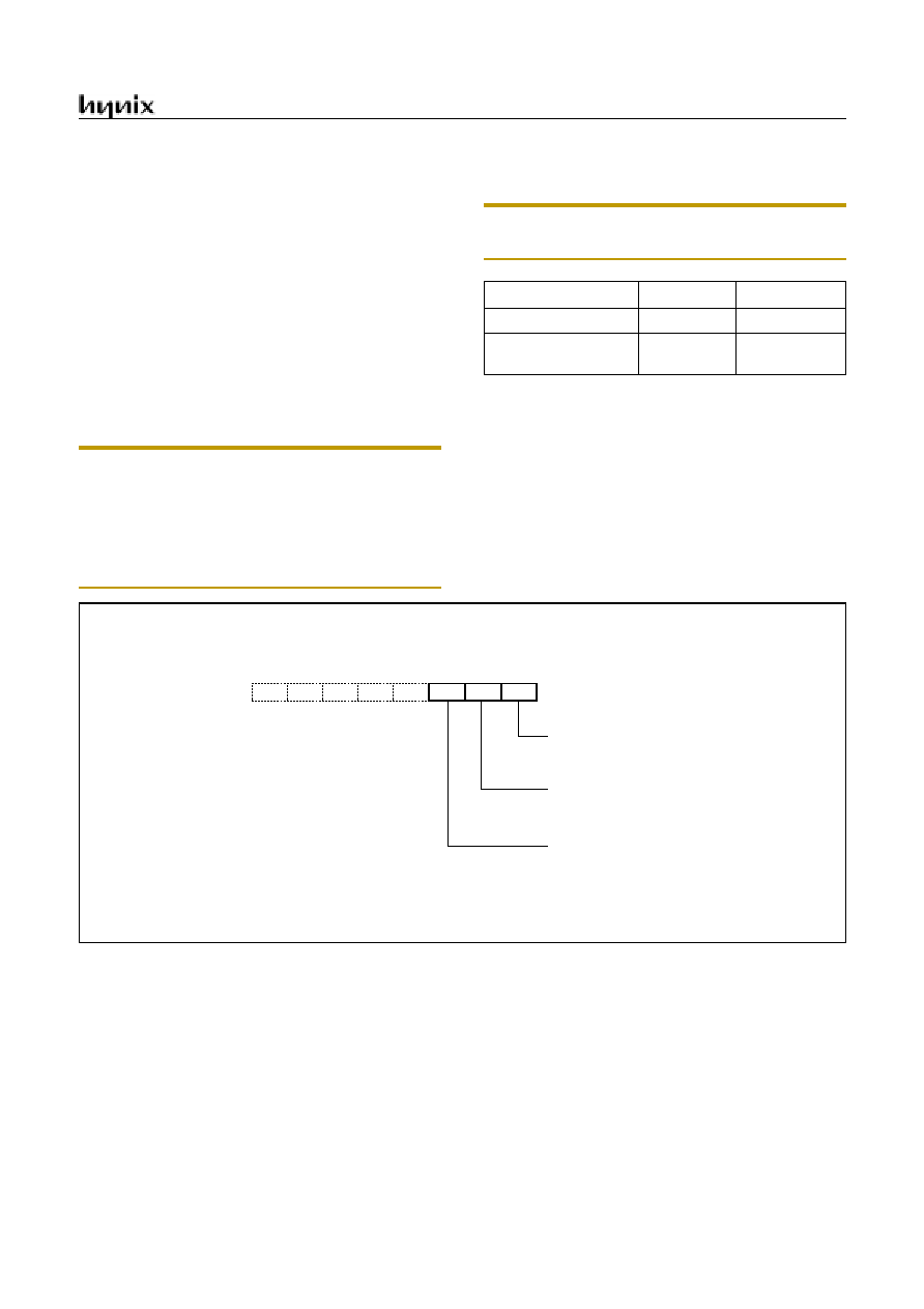
GMS81C2112/GMS81C2120
JUNE. 2001 Ver 1.00
81
20. POWER FAIL PROCESSOR
The GMS81C21xx has an on-chip power fail detection cir-
cuitry to immunize against power noise. A configuration
register, PFDR, can enable or disable the power fail detect
circuitry. Whenever V
DD
falls close to or below power fail
voltage for 100ns, the power fail situation may reset or
freeze MCU according to PFDM bit of PFDR. Refer to
"7.4 DC Electrical Characteristics for Standard Pins(5V)"
on page 14.
In the in-circuit emulator, power fail function is not imple-
mented and user can not experiment with it. Therefore, af-
ter final development of user program, this function may
be experimented or evaluated.
Note: User can select power fail voltage level according to
PFD0, PFD1 bit of CONFIG register(703F
H
) at the OTP
(GMS87C21xx) but must select the power fail voltage level
to define PFD option of "Mask Order & Verification Sheet"
at the mask chip(GMS81C21xx).
Because the power fail voltage level of mask chip
(GMS81C21xx) is determined according to mask option.
Note: If power fail voltage is selected to 3.0V on 3V oper-
ation, MCU is freezed at all the times.
Table 20-1 Power fail processor
.
Figure 20-1 Power Fail Voltage Detector Register
Power FailFunction
OTP
MASK
Enable/Disable
PFDIS flag
PFDIS flag
Level Selection
PFS0 bit
PFS1 bit
Mask option
PFDM
7
6
5
4
3
2
1
0
PFS
INITIAL VALUE: ---- -100
B
ADDRESS: 0EF
H
PFDR
R/W
R/W
R/W
PFDIS
Operation Mode
0 : Normal operation regardless of power fail
1 : MCU will be reset by power fail detection
Disable Flag
0: Power fail detection enable
1: Power fail detection disable
Power Fail Status
0: Normal operate
1: Set to "1" if power fail is detected
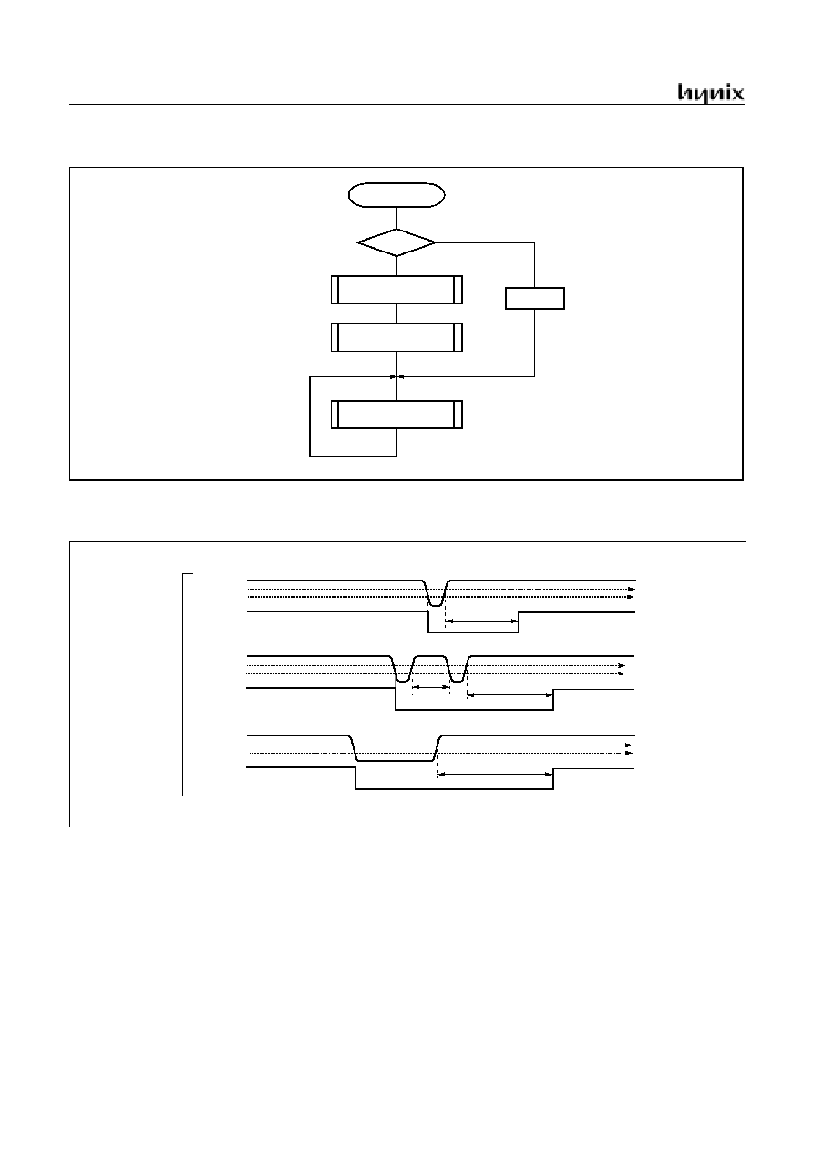
GMS81C2112/GMS81C2120
82
JUNE. 2001 Ver 1.00
Figure 20-2 Example S/W of RESET flow by Power fail
Figure 20-3 Power Fail Processor Situations
FUNTION
EXECUTION
INITIALIZE RAM DATA
PFS =1
NO
RESET VECTOR
INITIALIZE ALL PORTS
INITIALIZE REGISTERS
RAM CLEAR
YES
Skip the
initial routine
PFS = 0
Internal
RESET
Internal
RESET
Internal
RESET
V
DD
V
DD
V
DD
V
PFD
MAX
V
PFD
MIN
V
PFD
MAX
V
PFD
MIN
V
PFD
MAX
V
PFD
MIN
64mS
64mS
t <64mS
64mS
When PFR = 1
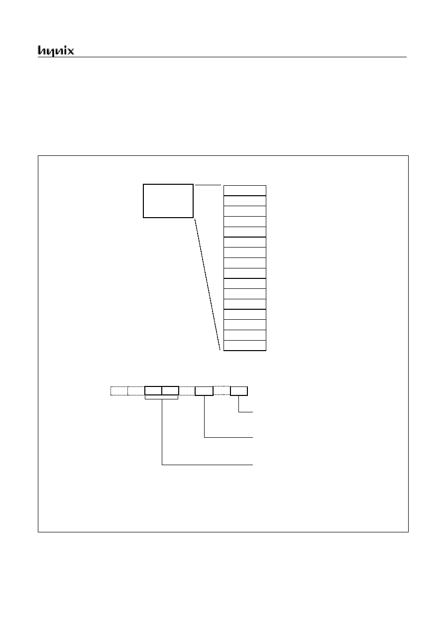
GMS81C2112/GMS81C2120
JUNE. 2001 Ver 1.00
83
21. OTP PROGRAMMING
21.1 DEVICE CONFIGURATION AREA
The Device Configuration Area can be programmed or left
unprogrammed to select device configuration such as secu-
rity bit.
Sixteen memory locations (7030
H
~ 703F
H
) are designated
as Customer ID recording locations where the user can
store check-sum or other customer identification numbers.
This area is not accessible during normal execution but is
readable and writable during program / verify.
Figure 21-1 Device Configuration Area
DEVICE
7030
H
7030
H
703F
H
703F
H
ID
CONFIG
CONFIGURATION
AREA
7031
H
ID
7032
H
ID
7033
H
ID
7034
H
ID
7035
H
ID
7036
H
ID
7037
H
ID
7038
H
ID
7039
H
ID
703A
H
ID
703B
H
ID
703C
H
ID
703D
H
ID
703E
H
ID
7
6
5
4
3
2
1
0
RCO
INITIAL VALUE: --00 -0-0
B
ADDRESS: 703F
H
CONFIG
LOCK
Code Protect
0 : Allow Code Read Out
1 : Lock Code Read Out
PFD Level Selection
00: PFD = 2.7V
01: PFD = 2.7V
External RC OSC Selection
0: Crystal or Resonator Oscillator
1: External RC Oscillator
PFS0
PFS1
10: PFD = 3.0V
11: PFD = 2.4V
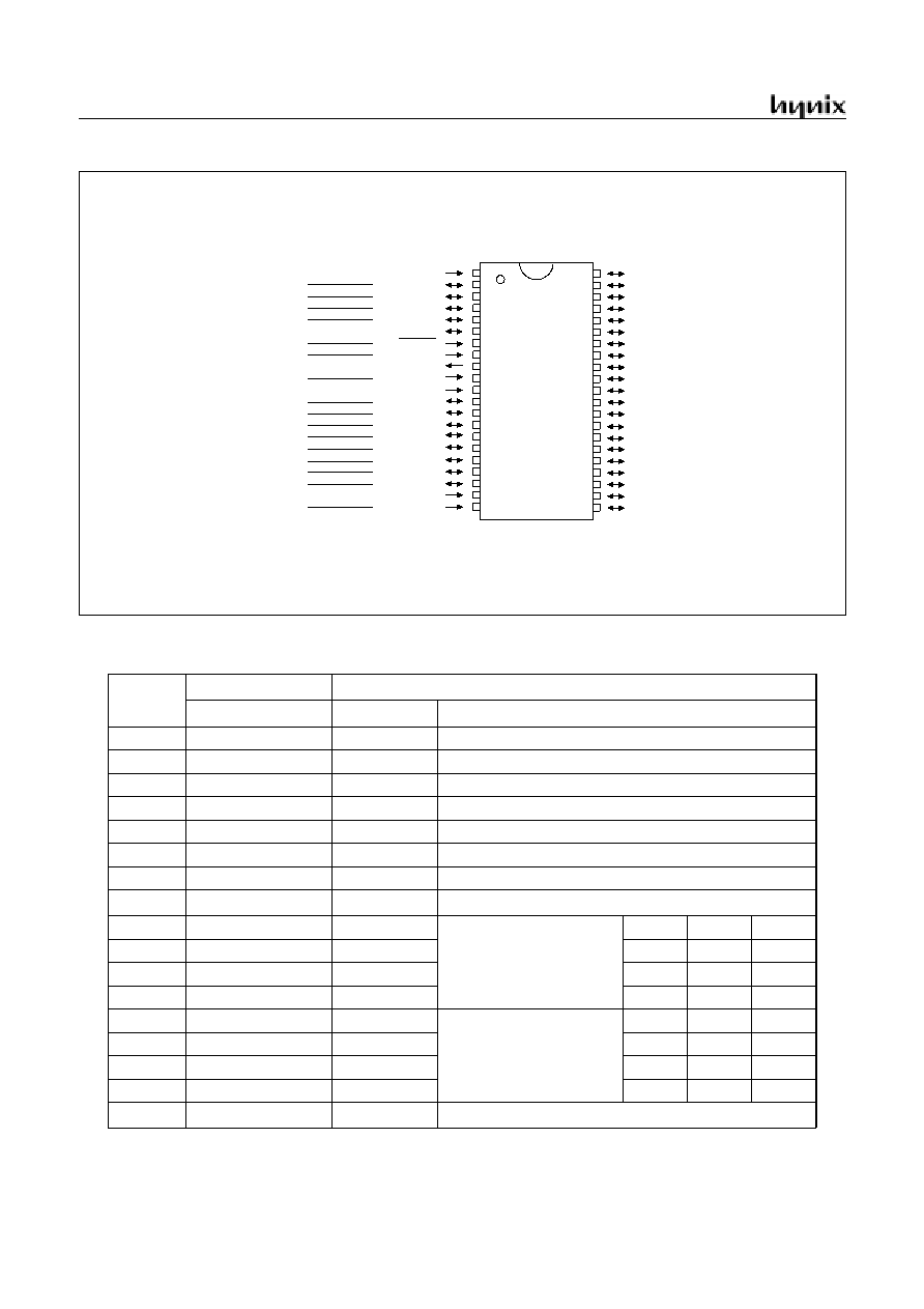
GMS81C2112/GMS81C2120
84
JUNE. 2001 Ver 1.00
Figure 21-2 Pin Assignment t
VPP
A_D0
A_D1
A_D2
A_D3
EPROM Enable
A_D7
A_D6
A_D5
A_D4
CTL2
CTL1
CTL0
V
SS
CTL3
R53
R54
R55
R56
R57
RESET
XI
XO
V
SS
AV
SS
R60
R61
R62
R63
R64
R65
R66
R67
AV
DD
RA
R34
R33
R32
R31
R30
R27
R26
R25
R24
R23
R22
R21
R20
R05
R04
R03
R02
R01
R00
V
DD
42PDIP
1
2
3
4
5
6
7
8
9
10
11
12
13
14
15
16
17
18
19
20
21
42
41
40
39
38
37
36
35
34
33
32
31
30
29
28
27
26
25
24
23
22
R07
R06
V
DD
Pin No.
User Mode
EPROM MODE
Pin Name
Pin Name
Description
2
R53
CTL3
Read/Write Control
3
R54
CTL2
Address/Data Control
4
R55
CTL1
Write Control 1
5
R56
CTL0
Write Control 0
7
RESETB
VPP
Programming Power (0V, 12.75V)
8
XI
EPROM Enable
High Active, Latch Address in falling edge
9
XO
NC
No connection
10
VSS
VSS
Connect to VSS
(0V)
12
R60
A_D0
Address Input
Data Input/Output
A8
A0
D0
13
R61
A_D1
A9
A1
D1
14
R62
A_D2
A10
A2
D2
15
R63
A_D3
A11
A3
D3
16
R64
A_D4
Address Input
Data Input/Output
A12
A4
D4
17
R65
A_D5
A13
A5
D5
18
R66
A_D6
A14
A6
D6
19
R67
A_D7
A15
A7
D7
21
VDD
VDD
Connect to VDD
(6.0V)
Table 21-1 Pin Description in EPROM Mode (GMS81C2120)
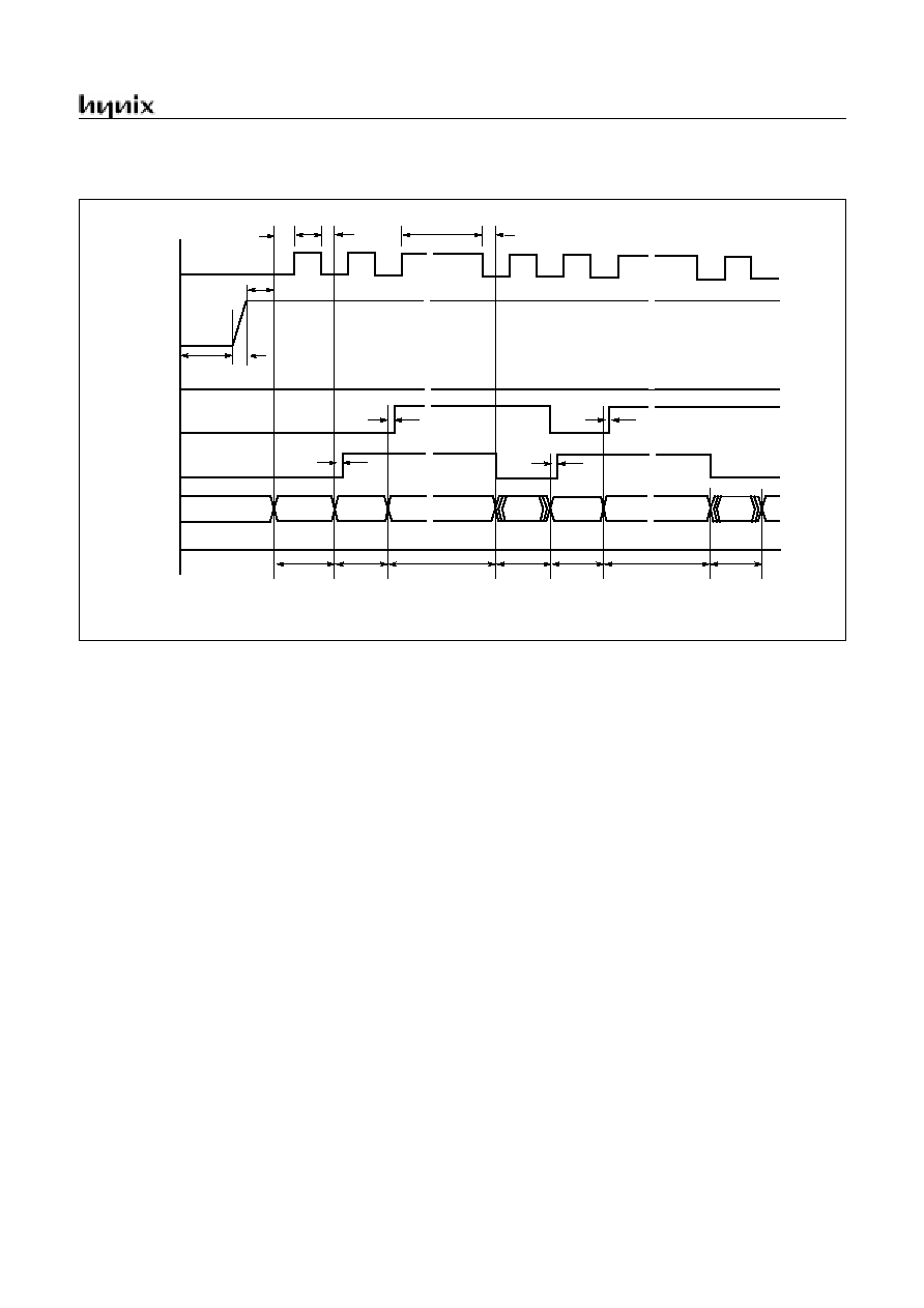
GMS81C2112/GMS81C2120
JUNE. 2001 Ver 1.00
85
Figure 21-3 Timing Diagram in Program (Write & Verify) Mode
VPP
CTL0/1
~~
High 8bit
HA
LA
DATA IN
DATA
~~
~~
~~
~~
OUT
LA
DATA IN
DATA
OUT
EPROM
Enable
CTL2
CTL3
A_D7~
VDD
V
DD1H
0V
0V
0V
Address
Input
Low 8bit
Address
Input
Write Mode
Verify
Low 8bit
Address
Input
Write Mode
Verify
A_D0
T
VDDS
T
VPPR
T
VPPS
~~
V
DD1H
V
DD1H
V
IHP
~~
~~
~~
~~
~~
~~
~~
~~
T
HLD1
T
HLD2
T
SET1
T
DLY1
T
DLY2
T
CD1
T
CD1
T
CD1
T
CD1
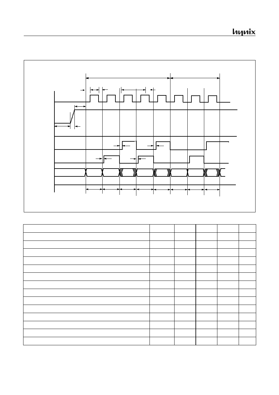
GMS81C2112/GMS81C2120
86
JUNE. 2001 Ver 1.00
Figure 21-4 Timing Diagram in READ Mode
Parameter
Symbol
MIN
TYP
MAX
Unit
Programming Supply Current
I
VPP
-
-
50
mA
Supply Current in EPROM Mode
I
VDDP
-
-
20
mA
VPP Level during Programming
V
IHP
11.5
12.0
12.5
V
VDD Level in Program Mode
V
DD1H
5
6
6.5
V
VDD Level in Read Mode
V
DD2H
-
2.7
-
V
CTL3~0 High Level in EPROM Mode
V
IHC
0.8V
DD
-
-
V
CTL3~0 Low Level in EPROM Mode
V
ILC
-
-
0.2V
DD
V
A_D7~A_D0 High Level in EPROM Mode
V
IHAD
0.9V
DD
-
-
V
A_D7~A_D0 Low Level in EPROM Mode
V
ILAD
-
-
0.1V
DD
V
VDD Saturation Time
T
VDDS
1
-
-
mS
VPP Setup Time
T
VPPR
-
-
1
mS
VPP Saturation Time
T
VPPS
1
-
-
mS
EPROM Enable Setup Time after Data Input
T
SET1
200
nS
EPROM Enable Hold Time after T
SET1
T
HLD1
500
nS
Table 21-2 AC/DC Requirements for Program/Read Mode
VPP
CTL0/1
High 8bit
HA
LA
DATA
LA
DATA
DATA
EPROM
Enable
CTL2
CTL3
A_D7~
VDD
V
DD2H
0V
0V
0V
Address
Input
Low 8bit
Address
Input
DATA
A_D0
T
VDDS
T
VPPR
T
VPPS
V
DD2H
V
DD2H
V
IHP
T
HLD1
T
HLD2
T
SET1
T
DLY1
T
DLY2
T
CD1
T
CD2
T
CD2
T
CD1
HA
LA
Output
Low 8bit
Address
Input
High 8bit
Address
Input
Low 8bit
Address
Input
DATA
Output
DATA
Output
After input a high address,
output data following low address input
Anothe high address step
GMS81C2112/GMS81C2120
JUNE. 2001 Ver 1.00
87
Figure 21-5 Programming Flow Chart
EPROM Enable Delay Time after T
HLD1
T
DLY1
200
nS
EPROM Enable Hold Time in Write Mode
T
HLD2
100
nS
EPROM Enable Delay Time after T
HLD2
T
DLY2
200
nS
CTL2,1 Setup Time after Low Address input and Data input
T
CD1
100
nS
CTL1 Setup Time before Data output in Read and Verify Mode
T
CD2
100
nS
Table 21-2 AC/DC Requirements for Program/Read Mode
START
Set VDD=V
DD1H
Set VPP=V
IHP
Verify blank
First Address Location
EPROM Write
N=1
Verify
Last address
Apply 3x program cycle
100uS program time
Next address location
N
Report
Programming failure
Verify of all address
VDD=6V & 2.7V
Report
Verify failure
Report
Programming OK
VDD=0V
END
FAIL
PASS
PASS
YES
FAIL
NO
FAIL
YES
PASS
VPP=0V
?
Verify
N=N+1
NO

GMS81C2112/GMS81C2120
88
JUNE. 2001 Ver 1.00

APPENDIX
GMS800 Series
JUNE. 2001
i
A. CONTROL REGISTER LIST
Address
Register Name
Symbol
R/W
Initial Value
Page
7 6 5 4 3 2 1 0
00C0
R0 port data register
R0
R/W
Undefined
34
00C1
R0 port I/O direction register
R0IO
W
0 0 0 0 0 0 0 0
34
00C4
R2 port data register
R2
R/W
Undefined
35
00C5
R2 port I/O direction register
R2IO
W
0 0 0 0 0 0 0 0
35
00C6
R3 port data register
R3
R/W
Undefined
35
00C7
R3 port I/O direction register
R3IO
W
- - - 0 0 0 0 0
35
00CA
R5 port data register
R5
R/W
Undefined
35
00CB
R5 port I/O direction register
R5IO
W
0 0 0 0 0 - - -
35
00CC
R6 port data register
R6
R/W
Undefined
35
00CD
R6 port I/O direction register
R6IO
W
0 0 0 0 0 0 0 0
35
00D0
Timer mode register 0
TM0
R/W
- - 0 0 0 0 0 0
44
00D1
Timer 0 register
T0
R
0 0 0 0 0 0 0 0
48
Timer 0 data register
TDR0
W
1 1 1 1 1 1 1 1
44
Capture 0 data register
CDR0
R
0 0 0 0 0 0 0 0
50
00D2
Timer mode register 1
TM1
R/W
0 0 0 0 0 0 0 0
44
00D3
Timer 1 data register
TDR1
W
1 1 1 1 1 1 1 1
44
PWM 1 period register
T1PPR
W
1 1 1 1 1 1 1 1
54
00D4
Timer 1 register
T1
R
0 0 0 0 0 0 0 0
48
PWM 1 duty register
T1PDR
R/W
0 0 0 0 0 0 0 0
54
Capture 1 data register
CDR1
R
0 0 0 0 0 0 0 0
50
00D5
PWM 1 High register
PWM1HR
W
- - - - 0 0 0 0
54
00DE
Buzzer driver register
BUR
W
1 1 1 1 1 1 1 1
63
00E0
Serial I/O mode register
SIOM
R/W
0 0 0 0 0 0 0 1
60
00E1
Serial I/O data register
SIOR
R/W
Undefined
60
00E2
Interrupt enable register high
IENH
R/W
0 0 0 0 - - - -
66
00E3
Interrupt enable register low
IENL
R/W
0 0 0 0 - - - -
66
00E4
Interrupt request flag register high
IRQH
R/W
0 0 0 0 - - - -
65
00E5
Interrupt request flag register low
IRQL
R/W
0 0 0 0 - - - -
65
00E6
External interrupt edge selection register
IEDS
R/W
- - - - 0 0 0 0
71
00EA
A/D converter mode register
ADCM
R/W
- 0 0 0 0 0 0 1
56
00EB
A/D converter data register
ADCR
R
Undefined
56
00EC
Basic interval timer mode register
BITR
R
0 0 0 0 0 0 0 0
38
Clock control register
CKCTLR
W
- 0 0 1 0 1 1 1
38
00ED
Watchdog Timer Register
WDTR
R
0 0 0 0 0 0 0 0
40
Watchdog Timer Register
WDTR
W
0 1 1 1 1 1 1 1
40
00EF
Power fail detection register
PFDR
R/W
- - - - - 1 0 0
81

GMS800 Series
ii
JUNE. 2001
00F4
R0 Function selection register
R0FUNC
W
- - - - 0 0 0 0
34
00F6
R5 Function selection register
R5FUNC
W
- 0 - - - - - -
35
00F7
R6 Function selection register
R6FUNC
W
0 0 0 0 0 0 0 0
35
00F9
R5 N-MOS open drain selection register
R5MPDR
W
0 0 0 0 0 - - -
35
00FA
System clock mode register
SCMR
R/W
- - - 0 0 - - -
73
00FB
RA port data register
RA
R
Undefined
34
Address
Register Name
Symbol
R/W
Initial Value
Page
7 6 5 4 3 2 1 0
GMS800 Series
JUNE. 2001
iii
B. INSTRUCTION
B.1 Terminology List
Terminology
Description
A
Accumulator
X
X - register
Y
Y - register
PSW
Program Status Word
#imm
8-bit Immediate data
dp
Direct Page Offset Address
!abs
Absolute Address
[ ]
Indirect expression
{ }
Register Indirect expression
{ }+
Register Indirect expression, after that, Register auto-increment
.bit
Bit Position
A.bit
Bit Position of Accumulator
dp.bit
Bit Position of Direct Page Memory
M.bit
Bit Position of Memory Data (000
H
~0FFF
H
)
rel
Relative Addressing Data
upage
U-page (0FF00
H
~0FFFF
H
) Offset Address
n
Table CALL Number (0~15)
+
Addition
x
Upper Nibble Expression in Opcode
y
Upper Nibble Expression in Opcode
-
Subtraction
×
Multiplication
/
Division
( )
Contents Expression
AND
OR
Exclusive OR
~
NOT
Assignment / Transfer / Shift Left
Shift Right
Exchange
=
Equal
Not Equal
0
Bit Position
1
Bit Position

GMS800 Series
iv
JUNE. 2001
B.2 Instruction Map
LOW
HIGH
00000
00
00001
01
00010
02
00011
03
00100
04
00101
05
00110
06
00111
07
01000
08
01001
09
01010
0A
01011
0B
01100
0C
01101
0D
01110
0E
01111
0F
000
-
SET1
dp.bit
BBS
A.bit,rel
BBS
dp.bit,rel
ADC
#imm
ADC
dp
ADC
dp+X
ADC
!abs
ASL
A
ASL
dp
TCALL
0
SETA1
.bit
BIT
dp
POP
A
PUSH
A
BRK
001
CLRC
SBC
#imm
SBC
dp
SBC
dp+X
SBC
!abs
ROL
A
ROL
dp
TCALL
2
CLRA1
.bit
COM
dp
POP
X
PUSH
X
BRA
rel
010
CLRG
CMP
#imm
CMP
dp
CMP
dp+X
CMP
!abs
LSR
A
LSR
dp
TCALL
4
NOT1
M.bit
TST
dp
POP
Y
PUSH
Y
PCALL
Upage
011
DI
OR
#imm
OR
dp
OR
dp+X
OR
!abs
ROR
A
ROR
dp
TCALL
6
OR1
OR1B
CMPX
dp
POP
PSW
PUSH
PSW
RET
100
CLRV
AND
#imm
AND
dp
AND
dp+X
AND
!abs
INC
A
INC
dp
TCALL
8
AND1
AND1B
CMPY
dp
CBNE
dp+X
TXSP
INC
X
101
SETC
EOR
#imm
EOR
dp
EOR
dp+X
EOR
!abs
DEC
A
DEC
dp
TCALL
10
EOR1
EOR1B
DBNE
dp
XMA
dp+X
TSPX
DEC
X
110
SETG
LDA
#imm
LDA
dp
LDA
dp+X
LDA
!abs
TXA
LDY
dp
TCALL
12
LDC
LDCB
LDX
dp
LDX
dp+Y
XCN
DAS
111
EI
LDM
dp,#imm
STA
dp
STA
dp+X
STA
!abs
TAX
STY
dp
TCALL
14
STC
M.bit
STX
dp
STX
dp+Y
XAX
STOP
LOW
HIGH
10000
10
10001
11
10010
12
10011
13
10100
14
10101
15
10110
16
10111
17
11000
18
11001
19
11010
1A
11011
1B
11100
1C
11101
1D
11110
1E
11111
1F
000
BPL
rel
CLR1
dp.bit
BBC
A.bit,rel
BBC
dp.bit,rel
ADC
{X}
ADC
!abs+Y
ADC
[dp+X]
ADC
[dp]+Y
ASL
!abs
ASL
dp+X
TCALL
1
JMP
!abs
BIT
!abs
ADDW
dp
LDX
#imm
JMP
[!abs]
001
BVC
rel
SBC
{X}
SBC
!abs+Y
SBC
[dp+X]
SBC
[dp]+Y
ROL
!abs
ROL
dp+X
TCALL
3
CALL
!abs
TEST
!abs
SUBW
dp
LDY
#imm
JMP
[dp]
010
BCC
rel
CMP
{X}
CMP
!abs+Y
CMP
[dp+X]
CMP
[dp]+Y
LSR
!abs
LSR
dp+X
TCALL
5
MUL
TCLR1
!abs
CMPW
dp
CMPX
#imm
CALL
[dp]
011
BNE
rel
OR
{X}
OR
!abs+Y
OR
[dp+X]
OR
[dp]+Y
ROR
!abs
ROR
dp+X
TCALL
7
DBNE
Y
CMPX
!abs
LDYA
dp
CMPY
#imm
RETI
100
BMI
rel
AND
{X}
AND
!abs+Y
AND
[dp+X]
AND
[dp]+Y
INC
!abs
INC
dp+X
TCALL
9
DIV
CMPY
!abs
INCW
dp
INC
Y
TAY
101
BVS
rel
EOR
{X}
EOR
!abs+Y
EOR
[dp+X]
EOR
[dp]+Y
DEC
!abs
DEC
dp+X
TCALL
11
XMA
{X}
XMA
dp
DECW
dp
DEC
Y
TYA
110
BCS
rel
LDA
{X}
LDA
!abs+Y
LDA
[dp+X]
LDA
[dp]+Y
LDY
!abs
LDY
dp+X
TCALL
13
LDA
{X}+
LDX
!abs
STYA
dp
XAY
DAA
111
BEQ
rel
STA
{X}
STA
!abs+Y
STA
[dp+X]
STA
[dp]+Y
STY
!abs
STY
dp+X
TCALL
15
STA
{X}+
STX
!abs
CBNE
dp
XYX
NOP
GMS800 Series
JUNE. 2001
v
B.3 Instruction Set
Arithmetic / Logic Operation
No.
Mnemonic
Op
Code
Byte
No
Cycle
No
Operation
Flag
NVGBHIZC
1
ADC #imm
04
2
2
Add with carry.
2
ADC dp
05
2
3
A
( A ) + ( M ) + C
3
ADC dp + X
06
2
4
4
ADC !abs
07
3
4
NV--H-ZC
5
ADC !abs + Y
15
3
5
6
ADC [ dp + X ]
16
2
6
7
ADC [ dp ] + Y
17
2
6
8
ADC { X }
14
1
3
9
AND #imm
84
2
2
Logical AND
10
AND dp
85
2
3
A
( A )
( M )
11
AND dp + X
86
2
4
12
AND !abs
87
3
4
N-----Z-
13
AND !abs + Y
95
3
5
14
AND [ dp + X ]
96
2
6
15
AND [ dp ] + Y
97
2
6
16
AND { X }
94
1
3
17
ASL A
08
1
2
Arithmetic shift left
18
ASL dp
09
2
4
N-----ZC
19
ASL dp + X
19
2
5
20
ASL !abs
18
3
5
21
CMP #imm
44
2
2
Compare accumulator contents with memory contents
( A ) - ( M )
22
CMP dp
45
2
3
23
CMP dp + X
46
2
4
24
CMP !abs
47
3
4
N-----ZC
25
CMP !abs + Y
55
3
5
26
CMP [ dp + X ]
56
2
6
27
CMP [ dp ] + Y
57
2
6
28
CMP { X }
54
1
3
29
CMPX #imm
5E
2
2
Compare X contents with memory contents
30
CMPX dp
6C
2
3
( X ) - ( M )
N-----ZC
31
CMPX !abs
7C
3
4
32
CMPY #imm
7E
2
2
Compare Y contents with memory contents
33
CMPY dp
8C
2
3
( Y ) - ( M )
N-----ZC
34
CMPY !abs
9C
3
4
35
COM dp
2C
2
4
1'S Complement : ( dp )
~( dp )
N-----Z-
36
DAA
DF
1
3
Decimal adjust for addition
N-----ZC
37
DAS
CF
1
3
Decimal adjust for subtraction
N-----ZC
38
DEC A
A8
1
2
Decrement
N-----Z-
39
DEC dp
A9
2
4
M
( M ) - 1
N-----Z-
40
DEC dp + X
B9
2
5
N-----Z-
41
DEC !abs
B8
3
5
N-----Z-
42
DEC X
AF
1
2
N-----Z-
43
DEC Y
BE
1
2
N-----Z-
7 6 5 4 3 2 1 0
"0"
C
GMS800 Series
vi
JUNE. 2001
44
DIV
9B
1
12
Divide : YA / X Q: A, R: Y
NV--H-Z-
45
EOR #imm
A4
2
2
Exclusive OR
46
EOR dp
A5
2
3
A
( A )
( M )
47
EOR dp + X
A6
2
4
48
EOR !abs
A7
3
4
N-----Z-
49
EOR !abs + Y
B5
3
5
50
EOR [ dp + X ]
B6
2
6
51
EOR [ dp ] + Y
B7
2
6
52
EOR { X }
B4
1
3
53
INC A
88
1
2
Increment
N-----ZC
54
INC dp
89
2
4
M
( M ) + 1
N-----Z-
55
INC dp + X
99
2
5
N-----Z-
56
INC !abs
98
3
5
N-----Z-
57
INC X
8F
1
2
N-----Z-
58
INC Y
9E
1
2
N-----Z-
59
LSR A
48
1
2
Logical shift right
60
LSR dp
49
2
4
N-----ZC
61
LSR dp + X
59
2
5
62
LSR !abs
58
3
5
63
MUL
5B
1
9
Multiply : YA
Y
×
A
N-----Z-
64
OR #imm
64
2
2
Logical OR
65
OR dp
65
2
3
A
( A )
( M )
66
OR dp + X
66
2
4
67
OR !abs
67
3
4
N-----Z-
68
OR !abs + Y
75
3
5
69
OR [ dp + X ]
76
2
6
70
OR [ dp ] + Y
77
2
6
71
OR { X }
74
1
3
72
ROL A
28
1
2
Rotate left through Carry
73
ROL dp
29
2
4
N-----ZC
74
ROL dp + X
39
2
5
75
ROL !abs
38
3
5
76
ROR A
68
1
2
Rotate right through Carry
77
ROR dp
69
2
4
N-----ZC
78
ROR dp + X
79
2
5
79
ROR !abs
78
3
5
80
SBC #imm
24
2
2
Subtract with Carry
81
SBC dp
25
2
3
A
( A ) - ( M ) - ~( C )
82
SBC dp + X
26
2
4
83
SBC !abs
27
3
4
NV--HZC
84
SBC !abs + Y
35
3
5
85
SBC [ dp + X ]
36
2
6
86
SBC [ dp ] + Y
37
2
6
87
SBC { X }
34
1
3
88
TST dp
4C
2
3
Test memory contents for negative or zero, ( dp ) - 00
H
N-----Z-
89
XCN
CE
1
5
Exchange nibbles within the accumulator
A
7
~A
4
A
3
~A
0
N-----Z-
No.
Mnemonic
Op
Code
Byte
No
Cycle
No
Operation
Flag
NVGBHIZC
7 6 5 4 3 2 1 0
"0"
C
7 6 5 4 3 2 1 0
C
7 6 5 4 3 2 1 0
C
GMS800 Series
JUNE. 2001
vii
Register / Memory Operation
No.
Mnemonic
Op
Code
Byte
No
Cycle
No
Operation
Flag
NVGBHIZC
1
LDA #imm
C4
2
2
Load accumulator
2
LDA dp
C5
2
3
A
( M )
3
LDA dp + X
C6
2
4
4
LDA !abs
C7
3
4
5
LDA !abs + Y
D5
3
5
N-----Z-
6
LDA [ dp + X ]
D6
2
6
7
LDA [ dp ] + Y
D7
2
6
8
LDA { X }
D4
1
3
9
LDA { X }+
DB
1
4
X- register auto-increment : A
( M ) , X
X + 1
10
LDM dp,#imm
E4
3
5
Load memory with immediate data : ( M )
imm
--------
11
LDX #imm
1E
2
2
Load X-register
12
LDX dp
CC
2
3
X
( M )
N-----Z-
13
LDX dp + Y
CD
2
4
14
LDX !abs
DC
3
4
15
LDY #imm
3E
2
2
Load Y-register
16
LDY dp
C9
2
3
Y
( M )
N-----Z-
17
LDY dp + X
D9
2
4
18
LDY !abs
D8
3
4
19
STA dp
E5
2
4
Store accumulator contents in memory
20
STA dp + X
E6
2
5
( M )
A
21
STA !abs
E7
3
5
22
STA !abs + Y
F5
3
6
--------
23
STA [ dp + X ]
F6
2
7
24
STA [ dp ] + Y
F7
2
7
25
STA { X }
F4
1
4
26
STA { X }+
FB
1
4
X- register auto-increment : ( M )
A, X
X + 1
27
STX dp
EC
2
4
Store X-register contents in memory
28
STX dp + Y
ED
2
5
( M )
X
--------
29
STX !abs
FC
3
5
30
STY dp
E9
2
4
Store Y-register contents in memory
31
STY dp + X
F9
2
5
( M )
Y
--------
32
STY !abs
F8
3
5
33
TAX
E8
1
2
Transfer accumulator contents to X-register : X
A
N-----Z-
34
TAY
9F
1
2
Transfer accumulator contents to Y-register : Y
A
N-----Z-
35
TSPX
AE
1
2
Transfer stack-pointer contents to X-register : X
sp
N-----Z-
36
TXA
C8
1
2
Transfer X-register contents to accumulator: A
X
N-----Z-
37
TXSP
8E
1
2
Transfer X-register contents to stack-pointer: sp
X
N-----Z-
38
TYA
BF
1
2
Transfer Y-register contents to accumulator: A
Y
N-----Z-
39
XAX
EE
1
4
Exchange X-register contents with accumulator :X
A
--------
40
XAY
DE
1
4
Exchange Y-register contents with accumulator :Y
A
--------
41
XMA dp
BC
2
5
Exchange memory contents with accumulator
42
XMA dp+X
AD
2
6
( M )
A
N-----Z-
43
XMA {X}
BB
1
5
44
XYX
FE
1
4
Exchange X-register contents with Y-register : X
Y
--------
GMS800 Series
viii
JUNE. 2001
16-BIT operation
Bit Manipulation
No.
Mnemonic
Op
Code
Byte
No
Cycle
No
Operation
Flag
NVGBHIZC
1
ADDW dp
1D
2
5
16-Bits add without Carry
YA
( YA ) + ( dp +1 ) ( dp )
NV--H-ZC
2
CMPW dp
5D
2
4
Compare YA contents with memory pair contents :
(YA)
-
(dp+1)(dp)
N-----ZC
3
DECW dp
BD
2
6
Decrement memory pair
( dp+1)( dp)
( dp+1) ( dp) - 1
N-----Z-
4
INCW dp
9D
2
6
Increment memory pair
( dp+1) ( dp)
( dp+1) ( dp ) + 1
N-----Z-
5
LDYA dp
7D
2
5
Load YA
YA
( dp +1 ) ( dp )
N-----Z-
6
STYA dp
DD
2
5
Store YA
( dp +1 ) ( dp )
YA
--------
7
SUBW dp
3D
2
5
16-Bits subtract without carry
YA
( YA ) - ( dp +1) ( dp)
NV--H-ZC
No.
Mnemonic
Op
Code
Byte
No
Cycle
No
Operation
Flag
NVGBHIZC
1
AND1 M.bit
8B
3
4
Bit AND C-flag : C
( C )
( M .bit )
-------C
2
AND1B M.bit
8B
3
4
Bit AND C-flag and NOT : C
( C )
~( M .bit )
-------C
3
BIT dp
0C
2
4
Bit test A with memory :
MM----Z-
4
BIT !abs
1C
3
5
Z
( A )
( M ) , N
( M
7
) , V
( M
6
)
5
CLR1 dp.bit
y1
2
4
Clear bit : ( M.bit )
"0"
--------
6
CLRA1 A.bit
2B
2
2
Clear A bit : ( A.bit )
"0"
--------
7
CLRC
20
1
2
Clear C-flag : C
"0"
-------0
8
CLRG
40
1
2
Clear G-flag : G
"0"
--0-----
9
CLRV
80
1
2
Clear V-flag : V
"0"
-0--0---
10
EOR1 M.bit
AB
3
5
Bit exclusive-OR C-flag : C
( C )
( M .bit )
-------C
11
EOR1B M.bit
AB
3
5
Bit exclusive-OR C-flag and NOT : C
( C )
~(M .bit)
-------C
12
LDC M.bit
CB
3
4
Load C-flag : C
( M .bit )
-------C
13
LDCB M.bit
CB
3
4
Load C-flag with NOT : C
~( M .bit )
-------C
14
NOT1 M.bit
4B
3
5
Bit complement : ( M .bit )
~( M .bit )
--------
15
OR1 M.bit
6B
3
5
Bit OR C-flag : C
( C )
( M .bit )
-------C
16
OR1B M.bit
6B
3
5
Bit OR C-flag and NOT : C
( C )
~( M .bit )
-------C
17
SET1 dp.bit
x1
2
4
Set bit : ( M.bit )
"1"
--------
18
SETA1 A.bit
0B
2
2
Set A bit : ( A.bit )
"1"
--------
19
SETC
A0
1
2
Set C-flag : C
"1"
-------1
20
SETG
C0
1
2
Set G-flag : G
"1"
--1-----
21
STC M.bit
EB
3
6
Store C-flag : ( M .bit )
C
--------
22
TCLR1 !abs
5C
3
6
Test and clear bits with A :
A - ( M ) , ( M )
( M )
~( A )
N-----Z-
23
TSET1 !abs
3C
3
6
Test and set bits with A :
A - ( M ) , ( M )
( M )
( A )
N-----Z-

GMS800 Series
JUNE. 2001
ix
Branch / Jump Operation
No.
Mnemonic
Op
Code
Byte
No
Cycle
No
Operation
Flag
NVGBHIZC
1
BBC A.bit,rel
y2
2
4/6
Branch if bit clear :
--------
2
BBC dp.bit,rel
y3
3
5/7
if ( bit ) = 0 , then pc
( pc ) + rel
3
BBS A.bit,rel
x2
2
4/6
Branch if bit set :
--------
4
BBS dp.bit,rel
x3
3
5/7
if ( bit ) = 1 , then pc
( pc ) + rel
5
BCC rel
50
2
2/4
Branch if carry bit clear
if ( C ) = 0 , then pc
( pc ) + rel
--------
6
BCS rel
D0
2
2/4
Branch if carry bit set
if ( C ) = 1 , then pc
( pc ) + rel
--------
7
BEQ rel
F0
2
2/4
Branch if equal
if ( Z ) = 1 , then pc
( pc ) + rel
--------
8
BMI rel
90
2
2/4
Branch if minus
if ( N ) = 1 , then pc
( pc ) + rel
--------
9
BNE rel
70
2
2/4
Branch if not equal
if ( Z ) = 0 , then pc
( pc ) + rel
--------
10
BPL rel
10
2
2/4
Branch if minus
if ( N ) = 0 , then pc
( pc ) + rel
--------
11
BRA rel
2F
2
4
Branch always
pc
( pc ) + rel
--------
12
BVC rel
30
2
2/4
Branch if overflow bit clear
if (V) = 0 , then pc
( pc) + rel
--------
13
BVS rel
B0
2
2/4
Branch if overflow bit set
if (V) = 1 , then pc
( pc ) + rel
--------
14
CALL !abs
3B
3
8
Subroutine call
15
CALL [dp]
5F
2
8
M( sp)
( pc
H
), sp
sp - 1, M(sp)
(pc
L
), sp
sp - 1,
if !abs, pc
abs ; if [dp], pc
L
( dp ), pc
H
( dp+1 ) .
--------
16
CBNE dp,rel
FD
3
5/7
Compare and branch if not equal :
--------
17
CBNE dp+X,rel
8D
3
6/8
if ( A )
( M ) , then pc
( pc ) + rel.
18
DBNE dp,rel
AC
3
5/7
Decrement and branch if not equal :
--------
19
DBNE Y,rel
7B
2
4/6
if ( M )
0 , then pc
( pc ) + rel.
20
JMP !abs
1B
3
3
Unconditional jump
21
JMP [!abs]
1F
3
5
pc
jump address
--------
22
JMP [dp]
3F
2
4
23
PCALL upage
4F
2
6
U-page call
M(sp)
( pc
H
), sp
sp - 1, M(sp)
( pc
L
),
sp
sp - 1, pc
L
( upage ), pc
H
"0FF
H
" .
--------
24
TCALL n
nA
1
8
Table call : (sp)
( pc
H
), sp
sp - 1,
M(sp)
( pc
L
),sp
sp - 1,
pc
L
(Table vector L), pc
H
(Table vector H)
--------
GMS800 Series
x
JUNE. 2001
Control Operation & Etc.
No.
Mnemonic
Op
Code
Byte
No
Cycle
No
Operation
Flag
NVGBHIZC
1
BRK
0F
1
8
Software interrupt : B
"1", M(sp)
(pc
H
), sp
sp-1,
M(s)
(pc
L
), sp
sp - 1, M(sp)
(PSW), sp
sp -1,
pc
L
( 0FFDE
H
) , pc
H
( 0FFDF
H
) .
---1-0--
2
DI
60
1
3
Disable all interrupts : I
"0"
-----0--
3
EI
E0
1
3
Enable all interrupt : I
"1"
-----1--
4
NOP
FF
1
2
No operation
--------
5
POP A
0D
1
4
sp
sp + 1, A
M( sp )
6
POP X
2D
1
4
sp
sp + 1, X
M( sp )
--------
7
POP Y
4D
1
4
sp
sp + 1, Y
M( sp )
8
POP PSW
6D
1
4
sp
sp + 1, PSW
M( sp )
restored
9
PUSH A
0E
1
4
M( sp )
A , sp
sp - 1
10
PUSH X
2E
1
4
M( sp )
X , sp
sp - 1
--------
11
PUSH Y
4E
1
4
M( sp )
Y , sp
sp - 1
12
PUSH PSW
6E
1
4
M( sp )
PSW , sp
sp - 1
13
RET
6F
1
5
Return from subroutine
sp
sp +1, pc
L
M( sp ), sp
sp +1, pc
H
M( sp )
--------
14
RETI
7F
1
6
Return from interrupt
sp
sp +1, PSW
M( sp ), sp
sp + 1,
pc
L
M( sp ), sp
sp + 1, pc
H
M( sp )
restored
15
STOP
EF
1
3
Stop mode ( halt CPU, stop oscillator )
--------
C. MASK ORDER SHEET
MASK ORDER & VERIFICATION SHEET
GMS81C21XX-HJ
1. Customer Information
Company Name
Application
Order Date
YYYY
Tel:
Fax:
Name &
Signature:
.O T P file
File Name
(Please check mark
into )
Customer should write inside thick line box.
40PDIP
42SDIP
44MQFP
( ) .OTP
YYWW
KOREA
GMS81C21XX-HJ
Customer's logo
Chollian
Internet
Hitel
Package
12K
20K
ROM Size (bytes)
Ma
sk
D
a
t
a
Check Sum ( )
2. Device Information
MM
DD
3000
H
(20K )
5000
H
(12K )
7 F F F
H
3. Marking Specification
Customer logo is not required.
YYWW
KOREA
GMS81C21XX-HJ
Customer's part number
If the customer logo must be used in the special mark, please submit a clean original of the logo.
4. Delivery Schedule
Date
Quantity
HYNIX Confirmation
YYYY
MM
DD
YYYY
MM
DD
Customer sample
Risk order
pcs
pcs
E-mail address:
5. ROM Code Verification
YYYY
MM
DD
Verification date:
Please confirm out verification data.
Check sum:
Tel:
Fax:
Name &
Signature:
E-mail address:
YYYY
MM
DD
Approval date:
I agree with your verification data and confirm you to
make mask set.
Tel:
Fax:
Name &
Signature:
E-mail address:
12 or 20
S et "00
H
" in blanked area
GMS81C21XX MASK OPTION LIST
2. CONFIG OPTION Check
Customer should write inside thick line box.
3. H/V Port OPTION Check (Pull-down Option Check )
4. Normal Port OPTION Check ( Pull-up Option Check )
RA without pull-down resistor
1. RA/Vdisp
Vdisp
7
6
5
4
3
2
1
0
RCO
INITIAL VALUE: --00 -0-0
B
ADDRESS: 703F
H
CONFIG
LOCK
Code Protect
0 : Allow Code Read Out
1 : Lock Code Read Out
PFD Level Selection
00: PFD = 2.7V
01: PFD = 2.7V
External RC OSC Selection
0: Crystal or Resonator Oscillator
1: External RC Oscillator
PFS0
PFS1
10: PFD = 3.0V
11: PFD = 2.4V
Port
Option
ON OFF
R60/AN0
R61/AN1
R62/AN2
R63/AN3
R64/AN4
R65/AN5
R66/AN6
R67/AN7
X
X
X
CONFIG Default Value : XX00X0X0
P o rt
O p tio n
O N O F F
R 5 3 /S C L K
R 54 /S IN
R 5 5/S O U T
R 5 6/P W M
R 57
Port
Option
ON OFF
R00/INT0
R01/INT1
R02/EC0
R03/BUZO
R04
R05
R06
R07
Port
Option
ON OFF
R20
R21
R22
R23
R24
R25
R26
R27
Port
Option
ON OFF
R30
R31
R32
R33
R34
ON : with pull-down resistor
OFF : without pull-down resistor
ON : with pull-up resistor
OFF : without pull-up resistor
(Please check mark
into )
X
Document Outline