8-Bit CMOS Microcontorller
GMS97C2051/L2051
HYUNDAI MicroElectonics
1
Features
Compatible with MCS-51
TM
Products
2 Kbytes of programmable EPROM
4.25V to 5.5V Operating Range (GMS97C2051)
2.70V to 3.6V Operating Range (GMS97L2051)
Version for 12MHz / 24 MHz Operating frequency (GMS97C2051)
Only 12MHz Operating frequency (GMS97L2051)
Two-Level Program Memory Lock with encryption array
128 bytes SRAM
15 Programmable I/O Lines
Two 16-Bit Timer/Counters
Programmable serial USART
Five Interrupt Sources
Direct LED Drive Outputs
On-Chip Analog Comparator
Low Power Idle and Power Down Modes
Description
The GMS97C2051/L2051 is a high-performance CMOS 8-bit microcontroller with 2Kbytes of programmable
EPROM. The device is compatible with the industry standard MCS-51
TM
instruction set and pinout. The HYUN-
DAI MicroElectronics GMS97C2051/L2051 is a powerful microcontroller which provides a highly flexible and
cost effective solution to many embedded control applications. The GMS97C2051/L2051 provides the following
standard features: 2Kbytes of EPROM, 128 bytes of RAM, 15 I/O lines, two 16-bit timer/counters, a five vector
two-level interrupt architecture, a full duplex serial port, a precision analog comparator, on-chip oscillator and
clock circuitry. In addition, the GMS97C2051/L2051 supports two software selectable power saving modes. The
Idle Mode stops the CPU while allowing the RAM, timer/counters, serial port and interrupt system to continue
functioning. The Power Down Mode saves the RAM contents but freezes the oscillator disabling all other chip
functions until the next hardware reset.
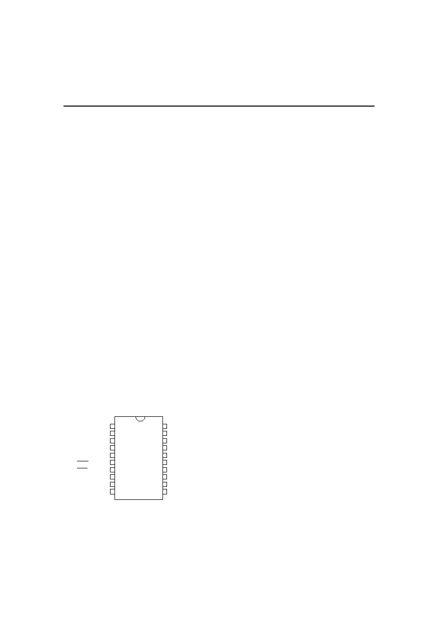
Pin Configuration
PDIP/SOP
(T0) P3.4
VCC
P1.7
P1.6
P1.5
P1.4
P1.3
P1.2
P1.1 (AIN1)
P1.0 (AIN0)
P3.7
RST
(RXD) P3.0
(TXD) P3.1
XTAL2
XTAL1
(
INT1
) P3.3
(T1) P3.5
GND
20
19
18
17
16
15
14
13
12
11
1
2
3
4
5
6
7
8
9
10
(
INT0
)P3.2
GMS97C2051/L2051
8-Bit CMOS Microcontroller
HYUNDAI MicroElectronics
2
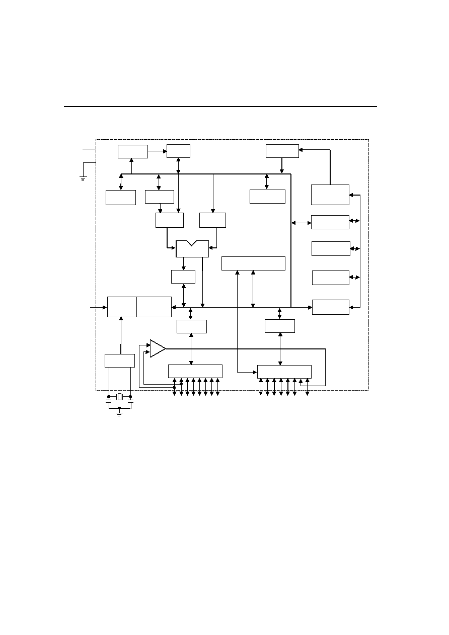
Block Diagram
VCC
GND
P1.0-P1.7
RAM
ADDR
RAM
STACK
POINTER
PC
INCREMENTER
PROGRAM
COUNTER
ACC
EPROM
PROGRAM
ADDRESS
REGISTER
BUFFER
DPTR
TMP1
TMP2
PSW
B
REGISTER
INTERRUPT, SERIAL PORT
AND TIMER BLOCKS
OSC
PORT 3
LATCH
PORT 1
LATCH
TIMING
AND
CONTROL
INSTRUCTION
REGISTER
+
_
PORT 1 DRIVERS
PORT 3 DRIVERS
RST
P3.0-P3.5 P3.7
ANALOG
COMPARATOR
ALU

8-Bit CMOS Microcontorller
GMS97C2051/L2051
HYUNDAI MicroElectonics
3
Pin Description
Vcc
Supply voltage.
GND
Ground.
Port 1
Port 1 is an 8-bit bidirectional I/O port. Port pins P1.2
to P1.7 provide internal pullups. P1.0 and P1.1 re-
quire external pullups. P1.0 and P1.1 also serve as the
positive input (AIN0) and the negative input (AIN1),
respectively, of the on-chip precision analog compara-
tor. The Port 1 output buffers can sink 10mA and can
drive LED displays directly. When 1s are written to
Port1 pins, they can be used as inputs. When pins
P1.2 to P1.7 are used as inputs and are externally pulled
low, they will source current (I
IL
) because of the inter-
nal pullups.
Port 1 also receives code data during EPROM pro-
gramming and program verification.
Port3
Port 3 pins P3.0 to P3.5, P3.7 are seven bidirectional
I/O pins with internal pullups. P3.6 is hard-wired as
an input to the output of the on-chip comparator and is
not accessible as a general purpose I/O pin. The Port
3 output buffers can sink 10mA. When 1s are written
to Port 3 pins they are pulled high by the internal pul-
lups and can be used as inputs. As inputs, Port 3 pins
that are externally being pulled low will source current
(I
IL
) because of the pullups.
Port 3 also serves the functions of various special fea-
ture of the GMS97C2051 as listed below:
Port Pin
Alternate Functions
P3.0
P3.1
P3.2
P3.3
P3.4
P3.5
RXD ( serial input port )
TXD ( serial output port )
INT0 ( external interrupt 0 )
INT1( external interrupt 1 )
T0 ( timer 0 external input )
T1 ( timer 0 external input )
Port 3 also receives some control signals for EPROM
programming and programming verification.
RST
Reset input. All I/O pins are reset to 1s as soon as
RST goes high. Holding the RST pin high for two
machine cycles while the oscillator is running resets the
device.
This pin is also receives the 12.75V programming
supply voltage ( Vpp ) during EPROM programming.
XTAL1
Input to the inverting oscillator amplifier and input to
the internal clock operating circuit.
XTAL2
Output from the inverting oscillator amplifier.
Recommended Oscillator Circuit
XTAL1 and XTAL2 are the input and output, respec-
tively, of an inverting amplifier which can be config-
ured for use as an on-chip oscillator, as shown in Fig-
ure 1. To drive the device from an external clock
source, XTAL2 should be left unconnected while
XTAL1 is driven as shown in Figure 2.
Figure 1. Oscillator Connections
C 2
C 1
X T A L 2
X T A L 1
G N D
Notes: C1, C2 = 30pF
10pF for Crystals
( include stray capacitance )
Figure 2. External Clock Drive Configuration
XTAL2
XTAL1
GND
EXTERNAL
OSCILLATOR
SIGNAL
NC

GMS97C2051/L2051
8-Bit CMOS Microcontroller
HYUNDAI MicroElectronics
4
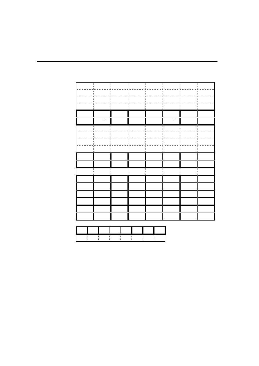
Special Function Registers
A map of the on-chip memory area called the Special
Function Register (SFR) space is shown in the Table1,
Table 2 and Table 3.
Note that not all of the addresses are occupied, and
unoccupied addresses may not be implemented on the
chip. Read accesses to these addresses will in general
return random data, and write accesses will have an
indeterminate effect.
User software should not write 1s to these unlisted
locations, since they may be used in future products to
invoke new features. In that case, the reset or inactive
values of the new bits will always be 0.
Table 1. GMS97C2051/L2051 SFR Map and Reset Values
0F8H
0FFH
0F0H
B
00000000
0F7H
0E8H
0EFH
0E0H
ACC
00000000
0E7H
0D8H
0DFH
0D0H
PSW
00000000
0D7H
0C8H
0CFH
0C0H
0C7H
0B8H
IP
XXX00000
0BFH
0B0H
P3
11111111
0B7H
0A8H
IE
0XX00000
0AFH
0A0H
0A7H
98H
SCON
00000000
SBUF
XXXXXXXX
9FH
90H
P1
11111111
97H
88H
TCON
00000000
TMOD
00000000
TL0
00000000
TL1
00000000
TH0
00000000
TH1
00000000
8FH
80H
SP
00000111
DPL
00000000
DPH
00000000
PCON
0XXX0000
87H
8-Bit CMOS Microcontorller
GMS97C2051/L2051
HYUNDAI MicroElectonics
5
Table 2. Bit Assignment of SFRs
Address Register
Bit7
Bit6
Bit5
Bit4
Bit3
Bit2
Bit1
Bit0
81
H
SP
82
H
DPL
83
H
DPH
87
H
PCON
SMOD
-
-
-
GF1
GF0
PD
IDLE
88
H
TCON
TF1
TR1
TF0
TR0
IE1
IT1
IE0
IT0
89
H
TMOD
GATE
C /
T
M1
M0
GATE
C /
T
M1
M0
8A
H
TL0
8B
H
TL1
8C
H
TH0
8D
H
TH1
90
H
P1
98
H
SCON
SM0
SM1
SM2
REN
TB8
RB8
TI
RI
99
H
SBUF
A8
H
IE
EA
-
-
ES
ET1
EX1
ET0
EX0
B0
H
P3
B8
H
IP
-
-
-
PS
PT1
PX1
PT0
PX0
D0
H
PSW
CY
AC
F0
RS1
RS0
OV
F1
P
E0
H
ACC
F0
H
B
- : This Bit Location is reserved
Bit manipulation is available
Bit manipulation is not available