18-BIT UNIVERSAL BUS DRIVER
HG74ALVC16835C
WITH 3-STATE OUTPUTS
Jan 1999
Copyright ©1999, Hyundai Electronics Industries Co., Ltd.
ELECTRONICS
1
Features
l
Ideal for Use in PC100 Registered DIMM
l
0.5
µ
m CMOS Technology
l
2.3 ~ 3.6 V
CC
Operation
l
Balanced Output Drive(
±
24mA)
l
Package Options Include Plastic Thin
Shrink Small-Outline Packages, Shrink
Small-Outline Packages
(TSSOP 56 Pins, SSOP 56 Pins, TVSOP56 Pins)
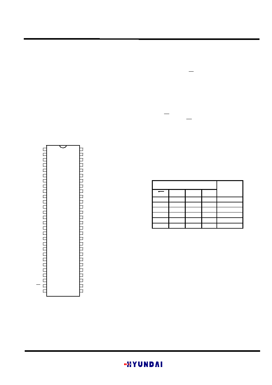
Pin Configuration
1
2
3
4
5
6
7
8
9
10
11
12
13
14
15
16
17
18
19
20
21
22
23
24
25
26
27
28
56
55
54
53
52
51
50
49
48
47
46
45
44
43
42
41
40
39
38
37
36
35
34
30
32
31
33
29
NC
NC
Y1
Y2
Y3
Vcc
Y4
Y5
Y6
GND
Y7
Y8
Y9
Y10
Y11
Y12
Y13
Y14
GND
Y15
Vcc
Y16
Y17
GND
Y18
OE
LE
GND
GND
NC
A1
GND
A2
A3
Vcc
A4
A5
A6
GND
A7
A8
A9
A10
A11
A12
GND
A13
A14
A15
Vcc
A16
A17
GND
A18
CLK
GND
NC- No ineternal connection
(TOP VIEW)
General Description
The HG74ALVC16835C is an 18-bit universal bus
driver designed for 2.3V to 3.6 V V
CC
Operation.
The Output-Enable(
OE
) controls data flow from A to Y.
The device operates in transparent mode when the
latch-enable(LE) input is high. When LE is low, the A
data is latched if the clock input is held at a high or low
logic level.
If LE is low, the A data is stored in the latch/flip-flop on
the low-to-high transition of CLK.
When
OE
is high, the Outputs are in the high
impedance state.
OE
should be tied to V
CC
through a
pull up resistor to ensure the high impedance state
during power up or power down.
The HG74ALVC16835C is characterized for operation
from -40
∞
C to 85
∞
C.
Function Table
INPUTS
LE
CLK
A
OUTPUT
Y
H
X
X
X
Z
L
H
X
L
L
L
H
X
H
H
L
L
L
L
L
L
H
H
L
L
L or H
X
Y
O
=
=
Output level before the indicated steady-state input
conditions were established, provided that CLK is high
before LE goes low.
OE
18-BIT UNIVERSAL BUS DRIVER
HG74ALVC16835C
WITH 3-STATE OUTPUTS
Jan 1999
Copyright ©1999, Hyundai Electronics Industries Co., Ltd.
ELECTRONICS
2
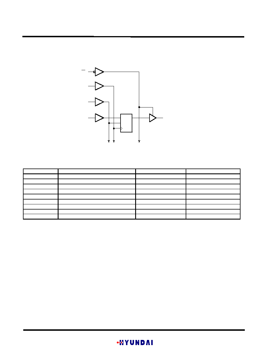
Logic Diagram (positive logic)
Absolute Maximum Ratings Over Operating Free-air Temperature Range
=
Symbols
Parameter
Value
Conditions
V
CC
Supply Voltage Range
-0.5 V to 4.6 V
V
I
Input Voltage Range (see note 1)
-0.5V to V
CC
+
0.5V
V
O
Output Voltage Range (see note 1 and 2)
-0.5V to V
CC
+
0.5V
I
IK
Input Clamp Current
±
50 mA
V
I
< 0
I
OK
Output Clamp Current
±
50 mA
V
O
<0 or V
O
>V
CC
I
O
Continuous Output Current
±
50 mA
V
O
=0 to V
CC
I
CC
Continuous Current through each V
CC
+
100 mA
I
GND
Continuous Current through each GND
-100 mA
T
stg
Storage Temperature Range
-65
∞
C to 150
∞
C
=
Stresses beyond those listed under " absolute maximum rating" may cause permanent damage to the device. These are stress ratings only, and
functional operation of the device at these or any other conditions beyond those indicated under "recommended operating condition" is not
implied. Exposure to absolute maximum-rated conditions for extended periods may affect device reliability.
Note 1) The input and output voltage ratings may be exceeded if the input and output clamp current are observed.
Note 2) This value is limited to 4.6 V maximum.
OE
CLK
LE
A1
Y1
27
30
28
54
3
1D
C1
CLK
TO 17 Other Channels
18-BIT UNIVERSAL BUS DRIVER
HG74ALVC16835C
WITH 3-STATE OUTPUTS
Jan 1999
Copyright ©1999, Hyundai Electronics Industries Co., Ltd.
ELECTRONICS
3
Recommended Operating Conditions (see Note 3)
Value
Symbols
Parameter
MIN
MAX
Units
Conditions
V
CC
Supply Voltage
2.3
3.6
V
1.7
V
V
CC
=2.3V to 2.7V
V
IH
High -level input Voltage
2
V
V
CC
=2.7V to 3.6V
0.7
V
V
CC
=2.3V to 2.7V
V
IL
Low-level input Voltage
0.8
V
V
CC
=2.7V to 3.6V
V
I
Input Voltage
0
V
CC
V
V
O
Output Voltage
0
V
CC
V
-12
mA
V
CC
=2.3V
-12
mA
V
CC
=2.7V
I
OH
High-level output current
-24
mA
V
CC
=3V
12
mA
V
CC
=2.3V
12
mA
V
CC
=2.7V
I
OL
Low-level output current
24
mA
V
CC
=3V
t/
v
Input transition rise or fall rate
0
10
ns/V
T
A
Operating free-air temperature
-40
85
∞
C
Note 3) All unused inputs of the device must be held at V
CC
or GND to ensure proper device operation.
Electrical Characteristics Over Recommended Operating Free-air Temperature Range
Value
Parameter
Test Conditions
Min
Typ
=
Max
Units
V
CC
I
OH
= -100
µ
A
V
CC
-
0.2
2.3V to 3.6V
I
OH
= - 6mA
V
IH
=1.7V
2
2.3V
V
IH
=1.7V
1.7
2.3V
2.2
2.7V
I
OH
= -12mA
V
IH
= 2V
2.4
3V
V
OH
I
OH
= -24 mA
V
IH
= 2V
2
V
3V
I
OL
= 100
µ
A
0.2
2.3V to 3.6V
I
OL
= 6mA
V
IL
= 0.7V
0.4
2.3V
V
IL
= 0.7V
0.7
2.3V
I
OL
= 12mA
V
IL
= 0.8V
0.4
2.7V
V
OL
I
OL
=24mA
V
IL
= 0.8V
0.55
V
3V
I
L
V
I
= V
CC
or GND
±
5
3.6V
I
OZ
V
O
= V
CC
or GND
±
10
3.6V
I
CC
V
I
= V
CC
or GND
I
O
= 0
40
3.6V
I
CC
One input at V
CC
- 0.6V,
Other inputs at V
CC
or GND
750
µ
A
3V to 3.6V
Control Inputs
3.5
C
I
Data Inputs
V
I
= V
CC
or GND
5
F
3.3V
C
o
Outputs
V
O
= V
CC
or GND
7
F
3.3V
=
All typical Values are at V
CC
=3.3V, T
A
= 25
∞
C.
18-BIT UNIVERSAL BUS DRIVER
HG74ALVC16835C
WITH 3-STATE OUTPUTS
Jan 1999
Copyright ©1999, Hyundai Electronics Industries Co., Ltd.
ELECTRONICS
4
Timing Requirements Over Recommended Operating Free-air Temperature Range(see figure1~10 )
Vcc=2.5V
±
0.2V
Vcc=2.7V
Vcc=3.3V
±
0.3V
Symbol
Parameter
Condition
Min
Max
Min
Max
Min
Max
Unit
f
clock
Clock
frequency
150
150
150
MHz
LE high
3.3
3.3
3.3
ns
t
W
Pulse
Duration
CLK high or low
3.3
3.3
3.3
ns
Data before CLK
0.9
0.9
0.7
ns
CLK high
1.9
1.6
1.5
ns
t
su
Setup time
Data before LE
CLK low
1.3
1.1
1
ns
Data after CLK
1.0
1.0
1.1
ns
t
h
Hold time
Data after LE
CLK high
or low
1.4
1.7
1.4
ns
Switching Characteristics Over Recommended Operating Free-air Temperature Range
V
CC
=2.5V
±
0.2V
V
CC
=2.7V
V
CC
=3.3V
±
0.3V
Parameter
Input
(From)
Output
(to)
Min
Max
Min
Max
Min
Max
Unit
f
max
150
150
150
MHz
A
1
4.2
4.2
1
3.6
ns
LE
1.3
5
4.9
1.3
4.2
ns
t
pd
CLK
Y
1.4
5.5
5.2
1.4
4.5
ns
t
en
Y
1.4
5.5
5.6
1.1
4.6
ns
I
dis
Y
1
4.5
4.3
1.3
3.9
ns
Switching Characteristics From 0
∞
C to 65
∞
C, C
L
=50
F
V
CC
=3.3V
±
0.15V
Parameter
Input
(From)
Output
(To)
Min
Max
Unit
t
pd
CLK
Y
1.7
4.5
ns
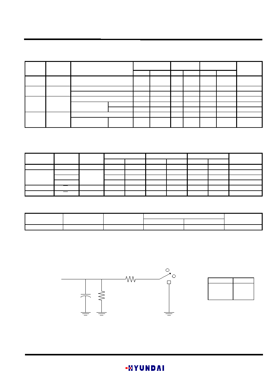
Parameter Measurement (V
CC
=2.5V
±
0.2V)
Note) C
L
includes probe and jig capacitance
Test
S1
t
pd
Open
t
PLZ
/ t
PZL
2 x V
CC
t
PHZ
/t
PZH
GND
Figure 1. Load Circuit
OE
OE
From Output
Under Test
C
L
= 30pF
(
see Note)
500
500
S1
2 x Vcc
Open
GND
18-BIT UNIVERSAL BUS DRIVER
HG74ALVC16835C
WITH 3-STATE OUTPUTS
Jan 1999
Copyright ©1999, Hyundai Electronics Industries Co., Ltd.
ELECTRONICS
5
Voltage Waveforms
Note 1 )Waveform1 is for an output with internal conditions such that the output is low except when disabled by the output control.
Waveform2 is for an output with internal conditions such that the output is high except when disabled by the output control
Note 2) All input pulses are supplied by generators having the following characteristics:
PRR
10Mhz, Z
o
= 50
, t
r
2ns, t
f
2ns.
Note 3) The output are measured one at a time with one transition per measurement.
Note 4) t
PLZ
and t
PHZ
are the same as t
dis
.
Note 5) t
PZL
and t
PZH
are the same as t
en
.
Note 6) t
PLH
and t
PHL
are the same as t
pd
.
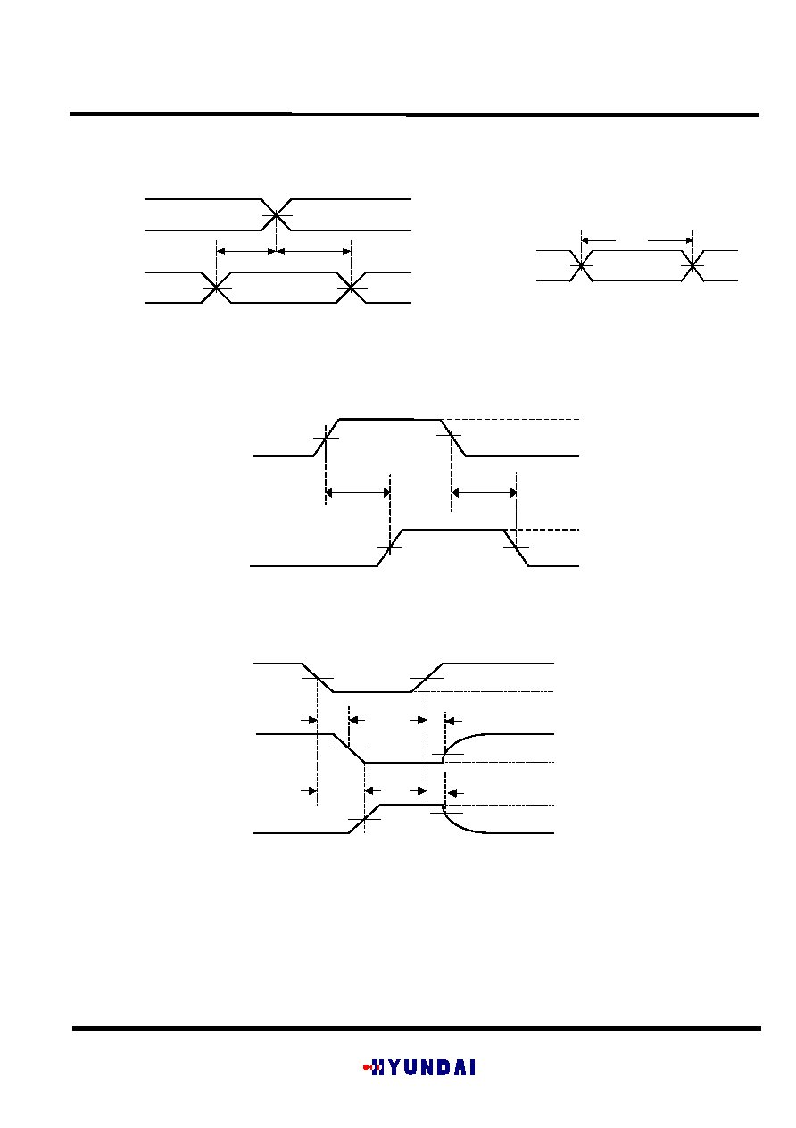
Timing
Input
Data
Input
V
CC
/2
t
su
t
h
Figure 2. Set up and Hold Times
V
CC
0V
V
CC
/2
V
CC
/2
Figure 3. Pulse Duration
Input
Output
t
PLH
t
PHL
V
CC
/2
V
CC
/2
V
CC
/2
V
CC
/2
V
OH
V
OL
Output Control
(Low-level enabling)
Output Waveform 1
S1 at 2 x V
CC
(See Note 1 )
Output Waveform 2
S1 at GND
(See Note 1 )
V
CC
/2
V
CC
/2
t
PZL
V
CC
/2
V
OL
+
0.15V
V
OH
-
0.15V
V
CC
0V
V
OL
V
OH
0V
Figure 5. Enable and Disable Times
V
CC
/2
t
PZH
t
PLZ
t
PHZ
V
CC
0V
t
w
V
CC
/2
V
CC
/2
V
CC
0V
V
CC
0V
Figure 4. Propagation Delay times
V
CC
Input