 | –≠–ª–µ–∫—Ç—Ä–æ–Ω–Ω—ã–π –∫–æ–º–ø–æ–Ω–µ–Ω—Ç: HM10S604 | –°–∫–∞—á–∞—Ç—å:  PDF PDF  ZIP ZIP |

∑
∑
CONFIDENTIAL & PROPRIETARY
CONFIDENTIAL & PROPRIETARY
HM10S604 PRELIMINARY SPEC
HM10S604
420/402CH
TFT-LCD
TFT-LCD SOURCE DRIVER
CMOS TFT-LCD SOURCE DRIVER
Electronics Industries
SPECIFICATION
PRELIMINARY
PRELIMINARY

∑
∑
CONFIDENTIAL & PROPRIETARY
CONFIDENTIAL & PROPRIETARY
HM10S604 PRELIMINARY SPEC
∑
Description
HM10S604 is a source driver LSI that drives an active-matrix LCD panels, as well as a 64
gradation driver that implements multi-pin configuration and reduced power consumption.
HM10S604 has 420/402 panel drive outputs. Because it is expandable, the HM10S604 can easily
be used in multiple application, its screen can be enlarged, and its L/R(shift-direction switching)
terminals can be used to simplify LCD panel interconnection.
The device has a large output dynamic range that makes the reverse driving of opposing
electrodes in the LCD panel unnecessary; this reduces system power consumption and produces
a high quality pictures. The device is also compatible with single sided mounting and dot reverse
driving.
The HM10S604's 420/402 outputs ensure SXGA+ compatibility, making it useful in a wider
range of applications.
The maximum operating clock frequency of the HM10S604 is 70MHz when the power supply
voltage for the logic section is between 2.7V and 3.6V and the single-side driving of an LCD panel
has been implemented.
∑
Features
Source Driver LSI for Active Matrix LCD
Compatible With Dot inversion, n-line inversion, column-line inversion
No Precharging
Liquid Crystal Outputs : 420/402
L/R(shift-direction switching) terminals can be used to simplify LCD panel interconnection.
Fine Pitch/TCP
Driver With Internal 6-Bit Digital Input DAC
Maximum Operating Clock Frequencies : 70MHz (Logic Section Power Supply : 2.7V - 3.6V)
Dual Port Input
Gamma Correction
No Need For an External Reference Voltage Generation Circuit(or for Ramp Voltage or a Multi-
Value Power Supply
Low System Power Consumption Can be Accomplished Using the Low Power Mode.
Can Handle Heavy Loads Using the LCD Capacity Switching Mode.
Allows for Input Data Reversing
Logic Section Power Supply Voltage : 2.7V - 3.6V
Liquid Crystal Drive Section Power Supply Voltage : 6V - 10V
CMOS TFT-LCD SOURCE DRIVER
Electronics Industries
∑
∑
CONFIDENTIAL & PROPRIETARY
CONFIDENTIAL & PROPRIETARY
HM10S604 PRELIMINARY SPEC
∑
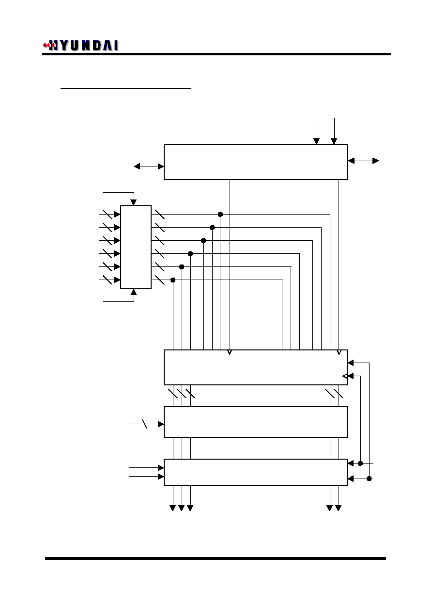
Functional Block Diagram
Output Buffer
Digital to Analog Converter
420/402 x 6 Bit x 2Line Latch
70 Bit Shift Register
Buffer
DF0 ~ DF5
DE0 ~ DE5
DD0 ~ DD5
DC0 ~ DC5
DB0 ~ DB5
DA0 ~ DA5
RVRS2
RVRS1
DEIO1
DEIO2
L/R DCLK
Voltage Reference
For Gamma Correction
(GH63/GH47/GH31/GH15/GH0
GL63/GL47/GL31/GL15/GL0)
LP
BC
LOAD
OUT1
OUT420
......................
......................
.....................
6
6
6
6
6
6
6
6
6
6
6
6
6 6 6
6 6
POLC
.......
10
∑
∑
CONFIDENTIAL & PROPRIETARY
CONFIDENTIAL & PROPRIETARY
HM10S604 PRELIMINARY SPEC
∑
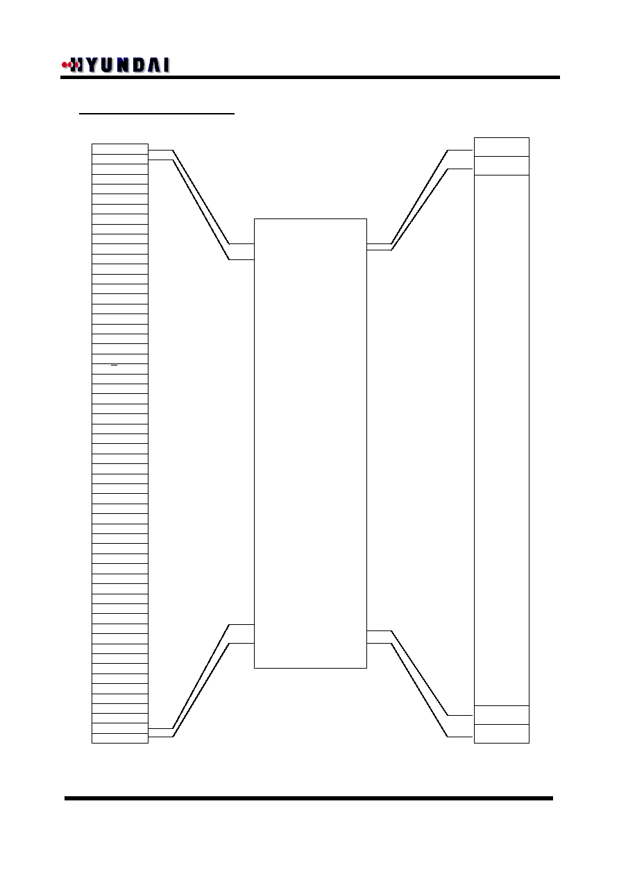
TCP Pin Configuration
HM10S604
OUT420
DEIO2
DF5
DF4
DF3
DF2
DF1
DF0
DE5
DE4
DE3
DE2
DE1
DE0
DD5
DD4
DD3
DD2
DD1
DD0
BC
LP
VDD1
L/R
GL63
GL47
GL31
GL15
GL0
VDD2
VSS
GH0
GH15
GH31
GH47
GH63
VSS
DCLK
LOAD
POLC
RVRS2
RVRS1
DC5
DC4
DC3
DC2
DC1
DC0
DB5
DB4
DB3
DB2
DB1
DB0
DA5
DA4
DA3
DA2
DA1
DA0
DEIO1
OUT1
OUT419
OUT2
∑
∑
CONFIDENTIAL & PROPRIETARY
CONFIDENTIAL & PROPRIETARY
HM10S604 PRELIMINARY SPEC
∑
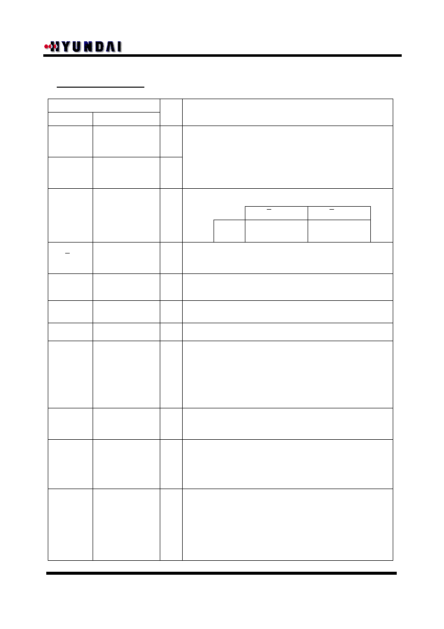
Terminal function
NAME
I/O
DESCRIPTION
DD0 - DD5
DE0 - DE5
DF0 - DF5
I
I
Image signal input terminal
Inputs image signals with a 36-bit width
: 6bit gradation data X 6 dots(for 2 pixels)
Data inputs which select between one of 64 voltages
Dx0 : LSB, Dx5 : MSB
Start pulse I/O
terminal
I/O
Internal shift register's start pulse
Right shift input
Right shift output
Left shift output
Left shift input
L/R=H
L/R=L
DEIO1
DEIO2
Shift direction selection signal
Right shift (OUT1 ---> OUT420) : H
Left shift (OUT420 ---> OUT1) : L
Shift direction
selection signal
input terminal
I
Shift register clock input terminal
Writes the display data to the data register at the leading edge
Shift clock Input
terminal
I
VDD1 Power supply for digital circuits.
VDD2 Power supply for analog circuits.
P
Potential input terminal for gamma correction
GH63 : The highest voltage in high voltage range.(necessary)
GH0 : The lowest voltage in high voltage range .(necessary)
GL0 : The highest voltage in low voltage range .(necessary)
GL63 : The lowest voltage in low voltage range .(necessary)
GH47/GL47, GH31/GL31, GH15/GL15
: Intermediate D/A voltage references (optional)
Gamma correction
reference potential
input terminal
I
Latches the data register contents with leading edge, transfers
it to the D/A converter, and outputs the gradation voltage with
trailing edge.
I
POLC= L : odd numbered outputs : GH63 ~ GH0
even numbered outputs : GL0 ~ GL63
POLC= H : odd numbered outputs : GL0 ~ GL63
even numbered outputs : GH63 ~ GH0
Polarity control
terminal
I
Selects reversal/non-reversal of input data
RVRS1 : controls reversal/non-reversal of port1.
RVRS2 : controls reversal/non-reversal of port2.
RVRS1,2 = H : reversal
RVRS1,2 = L : non-reversal
This terminal can be processed within TCP. H & L are
identified at the leading edge of each DCLK, like the data.
Input data reverse
terminal
I
TERMINAL
DA0 - DA5
DB0 - DB5
DC0 - DC5
Port1
Image signal input
terminal
Port2
Image signal input
terminal
DEIO1
DEIO2
L/R
DCLK
VDD1
VDD2
GHxx /
GLxx
LOAD
Latch input terminal
POLC
RVRS1
RVRS2
FUNCTION
VSS
Power supply
Ground
G
Ground for digital and analog
∑
∑
CONFIDENTIAL & PROPRIETARY
CONFIDENTIAL & PROPRIETARY
HM10S604 PRELIMINARY SPEC
I/O
DESCRIPTION
Sub-pixel output, provides 64 gray signals to the LCD panel.
O
Switched LCD drive capacity : BC = H : heavy load mode
BC = L : spec-load mode
I
Reduces charge and discharge current to a load
LP = H : normal mode
LP = L : low power mode
I
∑
Detailed description
Image signal capture
DEIOn=H(n=1 or n=2) is captured internally at the leading edge of DCLK. After the decay of DEIOn, the image signal
data are captured in the internal latch with the rise of the next DCLK.
If DEIOn receives an input in the meantime, new image signal data is captured at the rise of the next DCLK after
DEIOn decays.
It is possible to reverse the input data for each port by means of the RVRS1 and RVRS2.
Output expansion
The number of image signal output terminals can be expanded by cascading these devices,thereby enabling
compatibility with large screens. Expansion is controlled by using the L/R terminal:
L/R=L : the previous stage DEIO1 terminals is connected to the next stage DEIO2, and input terminals other
than DEIO1 and DEIO2 are connected together on each device.
L/R=H : the previous stage DEIO2 terminals is connected to the next stage DEIO1, and input terminals other
than DEIO1 and DEIO2 are connected together on each device
Relationship between input data values and output voltage
The output voltage is determined by the input data value and the 10 gamma correction potentials, Also, since
the output voltage is compatible with dot reverse driving, it is possible to output gradation voltages for the
opposing electrode voltages with polarities that differ for even and odd numbered outputs.
Input potentials with the same polarities relative to the opposing electrode voltages should be applied for
GH63/GL63,GH47/GL47,GH31/GL31,GH15/GL15,GH0/GL0 of the gamma correction reference power
supply.
Reference potential input for correction ( i.e. GH63/GL63,GH47/GL47,GH31/GL31,GH15/GL15,GH0/GL0 )
should be applied externally as desired. Reference potential should be maintained during gradation voltage
output. Refer to the operating conditions for the relative magnitude of each potential.
NAME
TERMINAL
LP
Low power mode
selection terminal
BC
LCD drive capacity
switching terminal
OUT1 ~
OUT420
LCD control
output terminal
FUNCTION
∑
∑
CONFIDENTIAL & PROPRIETARY
CONFIDENTIAL & PROPRIETARY
HM10S604 PRELIMINARY SPEC
∑
Detailed description (continued)
Details of pixel signal data
Data format : 6bit X 2 RGB
Input width : 36bits (2-pixel data)
Dx5
Dx4
Dx3
Dx2
Dx1
Dx0
MSB
LSB
Relationship between shift direction and output data:
Output
L/R = H (right shift)
Data
Out1
DA0-DA5
Out2
DB0-DB5
Out3
DC0-DC5
Out4
DD0-DD5
Out5
DE0-DE5
Out6
DF0-DF5
Out7
DA0-DA5
.......
.......
Out420
DF0-DF5
L/R = L (left shift)
Output
Data
Out1
DA0-DA5
Out2
DB0-DB5
Out3
DC0-DC5
Out4
DD0-DD5
Out5
DE0-DE5
Out6
DF0-DF5
Out7
DA0-DA5
.......
.......
Out420
DF0-DF5
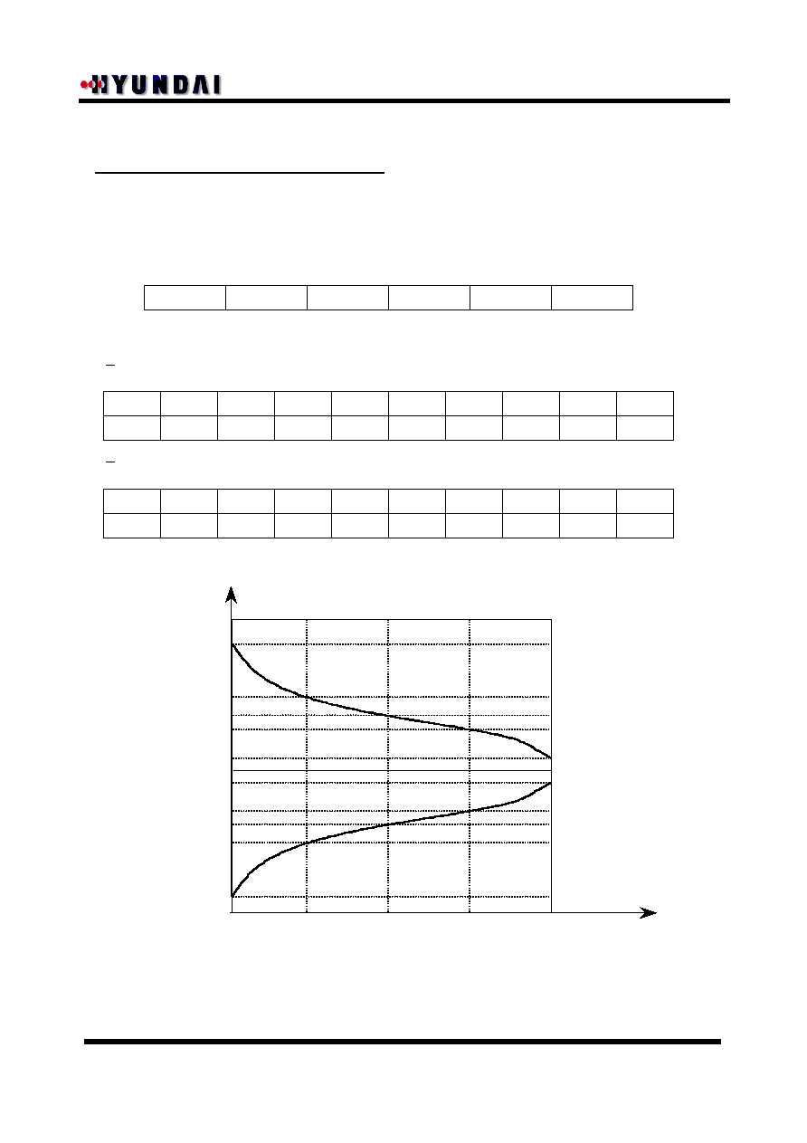
GH63
Voltage
Input Data (HEX)
GH47
GH31
GH15
GH0
VCOM
GL0
GL15
GL31
GL47
GL63
VDD1
VSS
Fig 1. Conceptional Drawing of Gamma Correction
∑
∑
CONFIDENTIAL & PROPRIETARY
CONFIDENTIAL & PROPRIETARY
HM10S604 PRELIMINARY SPEC
∑
Detailed description (continued)
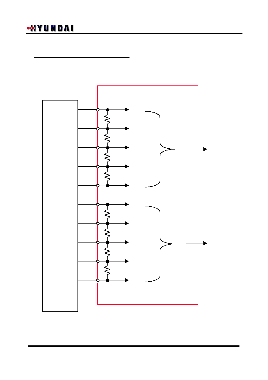
Resistance Between Reference Potential Input Terminals for Gamma Correction
External
Power
Supply
for
Reference
Power
RT1
RT2
RT5
RT8
GL63
GL0
GH0
GH63
Positive
Polarity
Negative
Polarity
RT3
RT4
RT6
RT7
GH47
GH31
GH15
GL15
GL31
GL47
HM10S604
∑
∑
CONFIDENTIAL & PROPRIETARY
CONFIDENTIAL & PROPRIETARY
HM10S604 PRELIMINARY SPEC
Resistance Between Reference Potential Input Terminals for Gamma Correction
Reference Potential
Name Resistance Ratio Reference Potential
Name Resistance Ratio
GH63 ,GL63
-
-
GH31,GL31
-
-
-
R0
R1
R2
R3
R4
R5
R6
R7
R8
R9
R10
R11
R12
R13
R14
R15
840
560
504
448
392
392
392
392
336
336
336
280
280
280
280
168
-
R32
R33
R34
R35
R36
R37
R38
R39
R40
R41
R42
R43
R44
R45
R46
R47
112
112
112
112
112
112
112
112
112
112
112
112
112
112
112
112
GH47,GL47
-
-
GH15,GL15
-
-
-
R16
R17
R18
R19
R20
R21
R22
R23
R24
R25
R26
R27
R28
R29
R30
R31
168
168
168
168
168
168
168
168
168
168
168
112
112
112
112
112
-
R48
R49
R50
R51
R52
R53
R54
R55
R56
R57
R58
R59
R60
R61
R62
112
112
112
112
112
168
168
168
168
168
224
280
280
616
1176
GH31,GL31
-
-
GH0,GL0
-
-
∑
Detailed description (continued)
∑
∑
CONFIDENTIAL & PROPRIETARY
CONFIDENTIAL & PROPRIETARY
HM10S604 PRELIMINARY SPEC
Relationship between Input data and output voltages at positive polarity
DATA
(Hex)
Dx[5:0]
00
000000
Output Voltage
GH63
Output Voltage
GH31
01
000001
GH47+(GH63 -GH47)X5376/6216
GH15+(GH31-GH15)X1680/1792
02
000010
GH47+(GH63 -GH47)X4816/6216
03
000011
GH47+(GH63 -GH47)X4312/6216
04
000100
GH47+(GH63 -GH47)X3864/6216
05
000101
GH47+(GH63 -GH47)X3472/6216
06
000110
GH47+(GH63 -GH47)X3080/6216
07
000111
GH47+(GH63 -GH47)X2688/6216
08
001000
GH47+(GH63 -GH47)X2296/6216
09
001001
GH47+(GH63 -GH47)X1960/6216
0A
001010
GH47+(GH63 -GH47)X1624/6216
0B
001011
GH47+(GH63 -GH47)X1288/6216
0C
001100
GH47+(GH63 -GH47)X1008/6216
0D
001101
GH47+(GH63 -GH47)X728/6216
0E
001110
GH47+(GH63 -GH47)X448/6216
0F
001111
GH47+(GH63 -GH47)X168/6216
10
010000
GH47
GH15
11
010001
GH31+(GH47-GH31)X2240/2408
GH0+(GH15-GH0)X3864/3976
12
010010
13
010011
14
010100
15
010101
16
010110
17
010111
18
011000
19
011001
1A
011010
1B
011011
1C
011100
1D
011101
1E
011110
1F
011111
DATA
(Hex)
20
21
22
23
24
25
26
27
28
29
2A
2B
2C
2D
2E
2F
30
31
32
33
34
35
36
37
38
39
3A
3B
3C
3D
3E
3F
Dx[5:0]
100000
100001
100010
100011
100100
100101
100110
100111
101000
101001
101010
101011
101100
101101
101110
101111
110000
110001
110010
110011
110100
110101
110110
110111
111000
111001
111010
111011
111100
111101
111110
111111
GH31+(GH47-GH31)X2072/2408
GH31+(GH47-GH31)X1904/2408
GH31+(GH47-GH31)X1736/2408
GH31+(GH47-GH31)X1568/2408
GH31+(GH47-GH31)X1400/2408
GH31+(GH47-GH31)X1232/2408
GH31+(GH47-GH31)X1064/2408
GH31+(GH47-GH31)X896/2408
GH31+(GH47-GH31)X728/2408
GH31+(GH47-GH31)X560/2408
GH31+(GH47-GH31)X448/2408
GH31+(GH47-GH31)X336/2408
GH31+(GH47-GH31)X224/2408
GH31+(GH47-GH31)X112/2408
GH15+(GH31-GH15)X1568/1792
GH15+(GH31-GH15)X1456/1792
GH15+(GH31-GH15)X1344/1792
GH15+(GH31-GH15)X1232/1792
GH15+(GH31-GH15)X1120/1792
GH15+(GH31-GH15)X1008/1792
GH15+(GH31-GH15)X896/1792
GH15+(GH31-GH15)X784/1792
GH15+(GH31-GH15)X672/1792
GH15+(GH31-GH15)X560/1792
GH15+(GH31-GH15)X448/1792
GH15+(GH31-GH15)X336/1792
GH15+(GH31-GH15)X224/1792
GH15+(GH31-GH15)X112/1792
GH0+(GH15-GH0)X3752/3976
GH0+(GH15-GH0)X3640/3976
GH0+(GH15-GH0)X3528/3976
GH0+(GH15-GH0)X3416/3976
GH0+(GH15-GH0)X3248/3976
GH0+(GH15-GH0)X3080/3976
GH0+(GH15-GH0)X2912/3976
GH0+(GH15-GH0)X2744/3976
GH0+(GH15-GH0)X2576/3976
GH0+(GH15-GH0)X2352/3976
GH0+(GH15-GH0)X2072/3976
GH0+(GH15-GH0)X1792/3976
GH0+(GH15-GH0)X1176/3976
GH0
∑
∑
CONFIDENTIAL & PROPRIETARY
CONFIDENTIAL & PROPRIETARY
HM10S604 PRELIMINARY SPEC
Relationship between Input data and output voltages at negative polarity
DATA
(Hex)
Dx[5:0]
00
000000
Output Voltage
GL63
Output Voltage
GL31
01
000001
GL63+(GL47-GL63)X840/6216
GL31+(GL15-GL31)X112/1792
02
000010
03
000011
04
000100
05
000101
06
000110
07
000111
08
001000
09
001001
0A
001010
0B
001011
0C
001100
0D
001101
0E
001110
0F
001111
10
010000
GL47
GL15
11
010001
GL47+(GL31-GL47)X168/2408
GL15+(GL0-GL15)X112/3976
12
010010
13
010011
14
010100
15
010101
16
010110
17
010111
18
011000
19
011001
1A
011010
1B
011011
1C
011100
1D
011101
1E
011110
1F
011111
DATA
(Hex)
20
21
22
23
24
25
26
27
28
29
2A
2B
2C
2D
2E
2F
30
31
32
33
34
35
36
37
38
39
3A
3B
3C
3D
3E
3F
Dx[5:0]
100000
100001
100010
100011
100100
100101
100110
100111
101000
101001
101010
101011
101100
101101
101110
101111
110000
110001
110010
110011
110100
110101
110110
110111
111000
111001
111010
111011
111100
111101
111110
111111
GL0
GL63+(GL47-GL63)X1400/6216
GL63+(GL47-GL63)X1904/6216
GL63+(GL47-GL63)X2352/6216
GL63+(GL47-GL63)X2744/6216
GL63+(GL47-GL63)X3136/6216
GL63+(GL47-GL63)X3528/6216
GL63+(GL47-GL63)X3920/6216
GL63+(GL47-GL63)X4256/6216
GL63+(GL47-GL63)X4592/6216
GL63+(GL47-GL63)X4928/6216
GL63+(GL47-GL63)X5208/6216
GL63+(GL47-GL63)X5488/6216
GL63+(GL47-GL63)X5768/6216
GL63+(GL47-GL63)X6048/6216
GL47+(GL31-GL47)X336/2408
GL47+(GL31-GL47)X504/2408
GL47+(GL31-GL47)X672/2408
GL47+(GL31-GL47)X840/2408
GL47+(GL31-GL47)X1008/2408
GL47+(GL31-GL47)X1176/2408
GL47+(GL31-GL47)X1344/2408
GL47+(GL31-GL47)X1512/2408
GL47+(GL31-GL47)X1680/2408
GL47+(GL31-GL47)X1848/2408
GL47+(GL31-GL47)X1960/2408
GL47+(GL31-GL47)X2072/2408
GL47+(GL31-GL47)X2184/2408
GL47+(GL31-GL47)X2296/2408
GL31+(GL15-GL31)X224/1792
GL31+(GL15-GL31)X336/1792
GL31+(GL15-GL31)X448/1792
GL31+(GL15-GL31)X560/1792
GL31+(GL15-GL31)X672/1792
GL31+(GL15-GL31)X784/1792
GL31+(GL15-GL31)X896/1792
GL31+(GL15-GL31)X1008/1792
GL31+(GL15-GL31)X1120/1792
GL31+(GL15-GL31)X1232/1792
GL31+(GL15-GL31)X1344/1792
GL31+(GL15-GL31)X1456/1792
GL31+(GL15-GL31)X1568/1792
GL31+(GL15-GL31)X1680/1792
GL15+(GL0-GL15)X224/3976
GL15+(GL0-GL15)X336/3976
GL15+(GL0-GL15)X448/3976
GL15+(GL0-GL15)X560/3976
GL15+(GL0-GL15)X728/3976
GL15+(GL0-GL15)X896/3976
GL15+(GL0-GL15)X1064/3976
GL15+(GL0-GL15)X1232/3976
GL15+(GL0-GL15)X1400/3976
GL15+(GL0-GL15)X1624/3976
GL15+(GL0-GL15)X1904/3976
GL15+(GL0-GL15)X2184/3976
GL15+(GL0-GL15)X2800/3976
∑
∑
CONFIDENTIAL & PROPRIETARY
CONFIDENTIAL & PROPRIETARY
HM10S604 PRELIMINARY SPEC
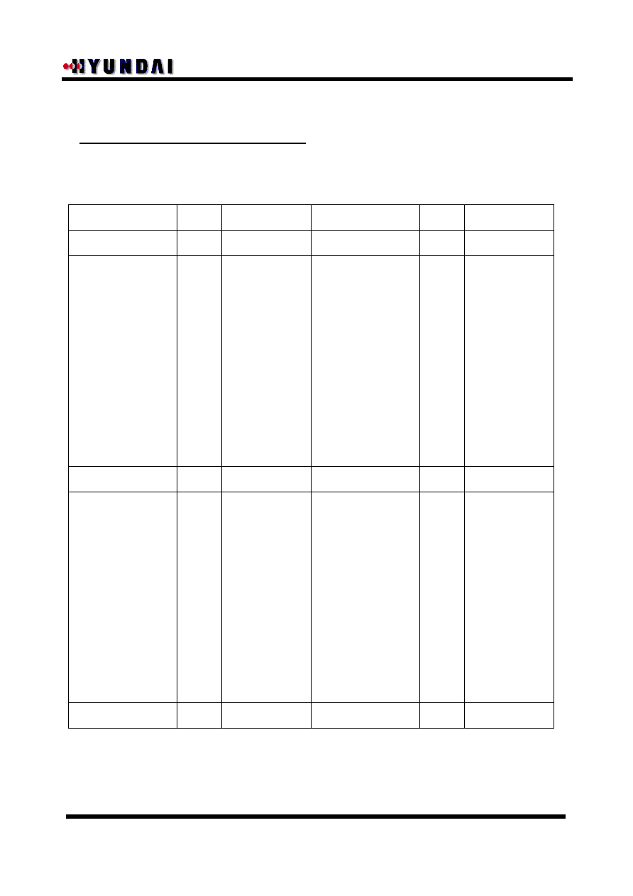
Absolute maximum ratings over operating free air temperature range(unless otherwise noted)
Parameter
Supply Voltage
Input Voltage
Output Voltage
VDD1(Note1&2)
VDD2
V
GMA
(Note3)
V
I
(Inputs)
V
O
(DEIO1,2)
V
O
(OUT1 ~ 420)
-0.5 ~ 5.5
-0.5 ~ 15.0
-0.5 ~ VDD2 + 0.5
-0.5 ~ VDD1 + 0.5
-0.5 ~ VDD1 + 0.5
-0.5 ~ VDD2 + 0.5
Absolute Maximum Ratings
Storage Temperature Range , T
STR
-55 ~ 125
V
V
V
V
V
V
Unit
Stresses beyond those listed under " absolute maximum ratings" may cause permanent damage to the
device. These are stress ratings only, and functional operation of the device at these or any other
conditions beyond those indicated under " recommended operating conditions" is not implied.
Exposure to absolute-maximum-rated conditions for extended periods may affect device reliability.
Notes : 1. All voltage values are with respect to VSS = 0V.
2. Power up in the following order : VDD1 , control inputs, VDD2, V
GMA
.
Power down by reversing the sequence.
3. V
GMA
= GH63/GL63,GH47/GL47,GH31/GL31,GH15/GL15,GH0/GL0
The relative magnitudes of the reference potentials are as follows:
VDD2 > GH63 > GH0 > GL0 > GL63>VSS
Parameter
Supply Voltage
Gamma correction potential
Clock frequency, f
clk
VDD1
VDD2
V
GMA
(GH63 ~ GH0)
V
GMA
(GL0 ~ GL63)
2.7 - 3.6
6.0 10.0
0.5*VDD2 VDD2-0.2
VSS+0.2 0.5*VDD2
75
MIN TYP MAX
Load capacitance for outputs, C
L
-10 75
V
V
V
V
pF
Unit
Output Voltage
V
O
(OUT1 ~OUT420)
VSS+0.2 VDD2-0.2
V
Operating free air temperature, T
A
2.7V
VDD1
3.6V
70
MHz
Recommended operating conditions
∑
∑
CONFIDENTIAL & PROPRIETARY
CONFIDENTIAL & PROPRIETARY
HM10S604 PRELIMINARY SPEC
Electrical characteristics over recommended operating conditions
Parameter
High level
input voltage
-
Test Conditions
V
Unit
Dx0~ Dx5,DCLK,
LOAD,RVRS1,RVRS2
DEIO1,DEIO2,
L/R,POLC,LP,BC
0.7VDD1 VDD1
MIN TYP MAX
Low level
input voltage
-
V
Dx0~ Dx5,DCLK,
LOAD,RVRS1,RVRS2
DEIO1,DEIO2,L/R,
POLC,LP,BC
0 0.3VDD1
Input leakage
current
-
uA
Dx0~ Dx5,DCLK,
LOAD,RVRS1,RVRS2
DEIO1,DEIO2,L/R,
POLC,LP,BC
10
Output
current
(Note 4)
Vx = VDD2 - 0.2 V
VO = Vx - 1.0 V
uA
OUT1 ~ OUT420
-110
I
CHG
I
DIS
Vx = VSS2+ 0.2 V
VO = Vx + 1.0 V
110
Deviation between
output voltage pins
(Note 5)
VSS + 0.2 ~
VDD2 - 0.2
mV
OUT1 ~ OUT420
10
Average output
variation (Note 6)
-
mV
OUT1 ~ OUT420
10
Resistance
between reference
power supplies
-
GH63 ~ GH0
GL0 ~ GL63
14,392
Supply current
(during operation)
LOAD interval = 20us
fclk = 36 MHz, No load
VDD2=8.0V
Black raster pattern
GH63 =7.8 V
GL63 = 0.2 V
uA
Analog section
TBD
Supply current
(during standby)
No load, VDD2=8V
Black raster pattern
GH63 =7.8 V
GL63 = 0.2 V
Clock and input signal
are in the stop state
uA
TBD
Supply current
(during operation)
LOAD interval = 20us
fclk = 36 MHz,
Checked dot test
pattern
uA
Digital section
TBD
SI
DD1
Clock and input signal
are in the stop state
uA
TBD
Notes : 4. Vx is the output voltage of OUT1 ~ OUT420. Vo is the voltage impressed at OUT1 ~ OUT420.
5.This is the deviation between terminals with differences in positive and negative amplitude,
when all chip outputs display the same data.
6. This is the inter-chip deviation in the average of the output voltage inter-pin deviation
R
GMA
DI
DD2
SI
DD2
DI
DD1
Supply current
(during standby)
V
AV
Vo
VIH
VIL
I
lk
∑
∑
CONFIDENTIAL & PROPRIETARY
CONFIDENTIAL & PROPRIETARY
HM10S604 PRELIMINARY SPEC
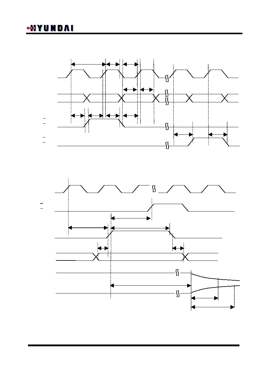
Timing requirements over recommended operating free air temperature range.
VDD1 = 2.7V to 3.6V
Parameter
DCLK cycle time
- See Fig 3.
Test Conditions
ns
Unit
14
MIN TYP MAX
High level DCLK pulse width duration
ns
2.0
Low level DCLK pulse width duration
ns
2.0
Data/REV setup time
ns
2.0
Data/REV hold time
ns
0
Start pulse setup time
ns
2.0
Start pulse hold time
ns
0
Start pulse signal delay time ( Load = 25pF)
ns
10
td2
5
td3
8
LCD drive signal delay time
LOAD signal EIO(input) setup time
DCLK cycle
2
LOAD low hold time from final data DCLK
DCLK cycle
1
High level LOAD signal pulse width duration
2
POLC signal LOAD setup time
ns
-5
POLC signal LOAD hold time
ns
6.0
- See Fig 3.
- See Fig 3.
- See Fig 3.
- See Fig 3.
- See Fig 3.
- See Fig 3.
- See Fig 3
- See Fig 4.note7,9
- See Fig 4.note8,9
- See Fig 4.
- See Fig 4.
- See Fig 4.
- See Fig 4.
- See Fig 4.
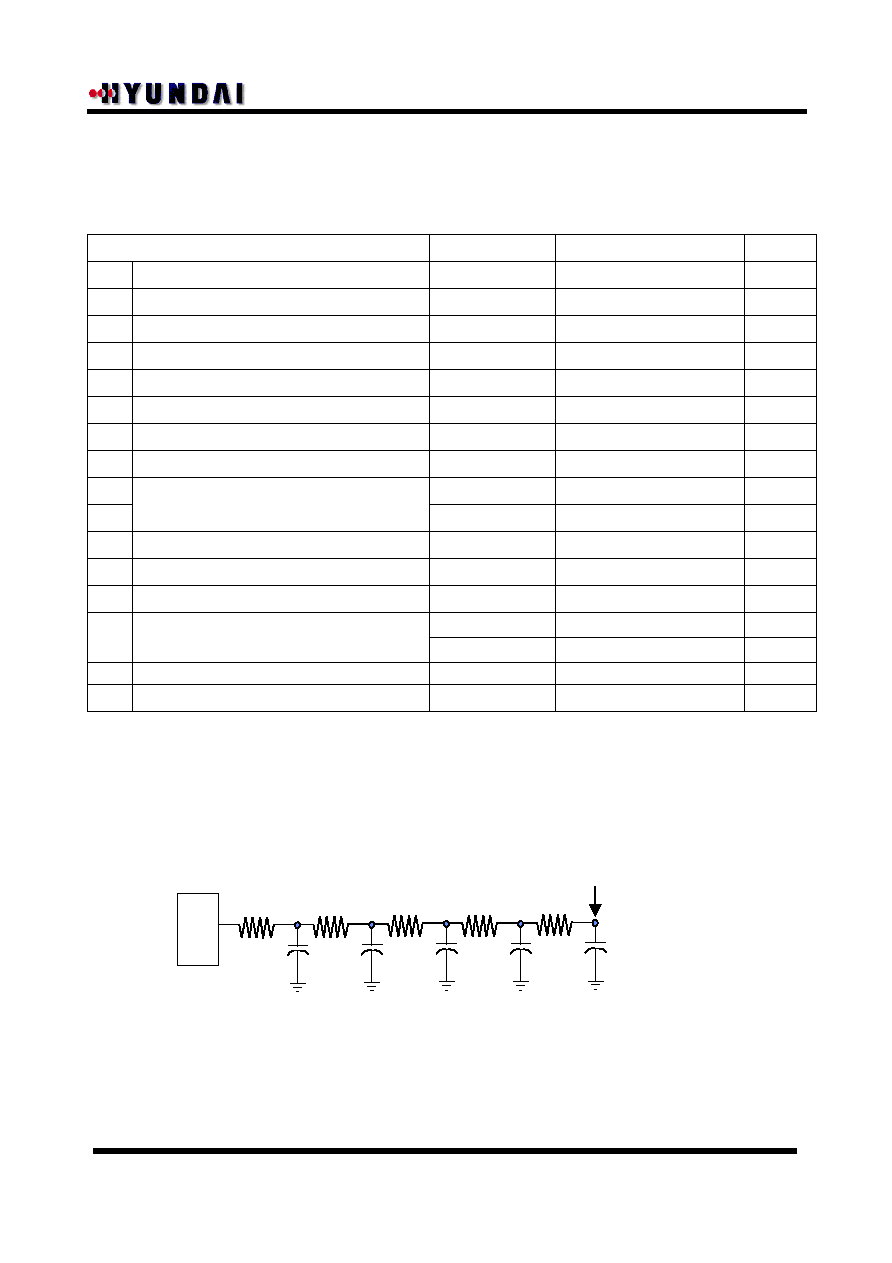
Fig 2. Load conditions of analog output pin.
The values of R and C could be changed according to the situation.
R = 1k
C = 15pF
Measured Point
OUTP
UT
R
C
R
C
R
C
R
C
R
C
tc1
tw1
tw2
tsu1
th1
tsu2
th2
td1
tsu3
th3
tw3
tsu4
th4
DCLK cycle
Output high impedance duration
66
- See Fig 4.note 10
thiz
DCLK cycle
tw3+3 DCLK cycle
- See Fig 5.note 11
-
Notes : 7. Specified as the value at which the driver's output voltage reaches the target output voltage
(VDD2X0.1).
8. Specified as the value at which ther driver's output voltage reaches the target output voltage(6-bit precision)
9. The load of the analog output terminal is the value shown in Fig 2.
10. When LOAD high level pulse width duration is shorter than 63 DCLK cycle, high-Z duration is 66 DCLK cycle.
11. When LOAD high level pulse width duration is longer than 63 DCLK cycle, high-Z duration is tw3+3DCLK cycle.
∑
∑
CONFIDENTIAL & PROPRIETARY
CONFIDENTIAL & PROPRIETARY
HM10S604 PRELIMINARY SPEC
tc1
tw1
tw2
th2
tsu2
th2
tsu2
tsu1
th1
1
2
69
70
LAST
(70)
LAST-1
(69)
td1
td1
DCLK
Dxx
RVRS1
RVRS2
DEIO1(L/R=H)
DEIO2(L/R=L)
INPUT
DEIO2(L/R=H)
DEIO1(L/R=L)
OUTPUT
Fig 3. Timing Waveform
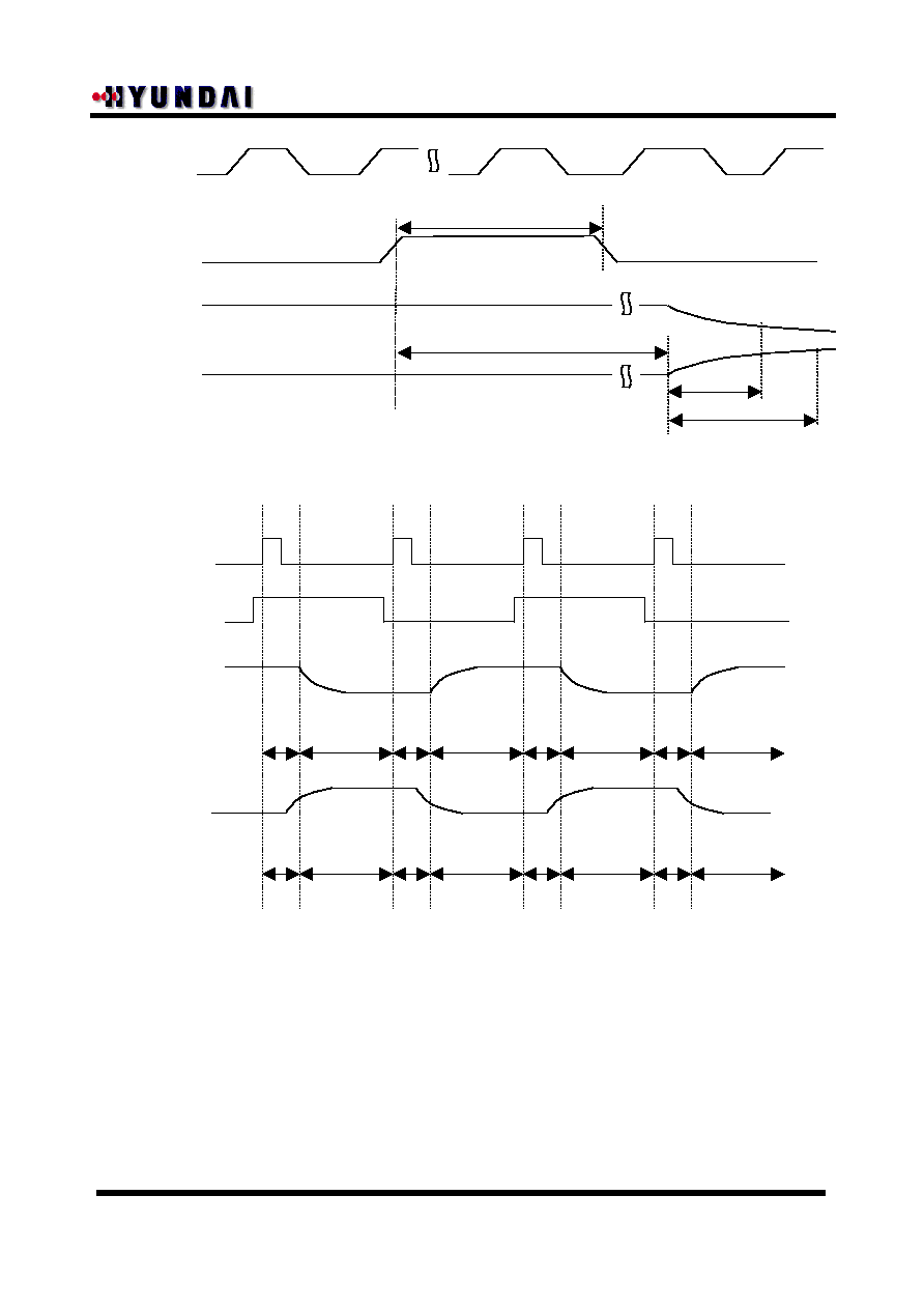
tsu3
th3
LAST
(70)
tsu4
DCLK
LOAD
DEIO1(L/R=H)
DEIO2(L/R=L)
INPUT
th4
POLC
High - Z
td2
td3
OUT ( H--> L)
OUT ( L--> H)
Fig 4. Timing Waveform
thiz
tw3 < 63 DCLK cycle
∑
∑
CONFIDENTIAL & PROPRIETARY
CONFIDENTIAL & PROPRIETARY
HM10S604 PRELIMINARY SPEC
POLC
Odd Outputs
Fig 6. Relationship between LOAD, POLC, and outputs
LOAD
High-Z
High-Z
High-Z
High-Z
GL63 ~GL0
GL63 ~GL0
GH63 ~GH0
GH63 ~GH0
Even Outputs
High-Z
High-Z
High-Z
High-Z
GH63 ~GH0
GH63 ~GH0
GL63 ~GL0
GL63 ~GL0
DCLK
LOAD
High - Z
td2
td3
OUT ( H--> L)
OUT ( L--> H)
Fig 5. Timing Waveform
thiz
Tw3 > 63 DCLK cycle