- 1 -
HM17CM256
128XRGBX82 OUTPUT LCD DRIVER IC
with built-in RAM
s
INSTRUCTION
HM17CM256 is a dot-Matrix LCD drive IC with 82
commons (80 + 2 icons) and 384 segments (128 X
RGB) drive ports for 256 colors driving.
This IC stores the serial or parallel BIT data
transferred by the microcomputer on the built-in
RAM (81,920 bits for graphic + 2048 bits for icons)
and generates the signals to drive LCD panel.
Color graphic display is achieved by selecting 8
gray (256 color) levels out of 32 gray palettes
independently.
This IC is suitable for battery-operated system,
hand-carrying information equipment by ensuring
low power consumption, low power supply (1.7V ~ )
and a wide range of operating voltage.
And 164 x 128 display (maximum) is possible with
master and slave application.
s
FEATURES
256 color bitmap LCD driver
�
LCD drive outputs 128
�
RGB segments, 80 commons for graphic and 2 commons for icons
�
Display RAM capacity 81,920bits (for graphic usage)
2,048bits (for icon usage)
�
Gradation display 8 gradations can be selected from 32 gradations by PWM control
�
Black/White display 82
�
(128
�
3) bits display is possible
�
8 bit BUS interface directly connectable with 68 / 80 series CPU
�
RAM data length 8 BIT / 16 BIT selectable
�
Serial interface available
�
Programmable duty / bias ratio with command
�
Various instruction set
display data read/write, display ON/OFF, positive/negative display, page address set
display start line address set, partial display, bias select,
column address set, all display ON/OFF, boosting selection, n line inversion mode
read modified write, power save ...
�
Built-in voltage booster (programmable) : 7
�
boosting
�
Built-in voltage regulator
�
Controllable contrast with built-in electric volume (128 steps)
�
Low current consumption
�
Logic supply 1.7V ~ 3.3V
�
LCD drive supply 5.0V ~ 18.0V
�
C-MOS silicon process
�
Package bumped chip / bare chip
Preliminary Specification(0.3)
HM17CM256
�
EXTERNAL SHAPE
01/02/09

HM17CM256
- 2 -
PAD LAYOUT
note 1) The (L) (R) (C) mark after port name is internally shorted.
note 2) DMYport is opened electrically.
chip center : X= 0
�
�
m, Y= 0
�
�
m
chip size : with scribe lane : 19.84mm x 2.48mm ,
main chip : 19.74mm x 2.38mm
chip thickness : 625
�
�
m
�
�
25
�
�
m
bump size : 100
�
�
m x 32
�
�
m, 100
�
�
m x 80
�
�
m
bump pitch : 50
�
�
m(Min)
bump height : 18
�
�
3
�
�
m
bump material : Au
align mark appearance and size
a : 30
�
�
m
b : 6
�
�
m
c : 120
�
�
m
d : 27
�
�
m
coordinates of align marks
(X= - 9732
�
�
m, Y= -1052
�
�
m)
(X= 9732
�
�
m, Y= -1052
�
�
m)
a
a c
c
b
b
d
d
1
D
M
Y
5
(
R
)
SE
G
A
125
D
M
Y
5
(
L
)
SE
G
B
125
SE
G
C
125
SE
G
A
126
SE
G
B
126
SE
G
C
126
SE
G
A
127
SE
G
B
127
SE
G
C
127
COM
40
SEGSC
3
SEGSA
2
DMY
6
(R)
DMY
6
(L)
DMY
7
(R)
DMY
7
(L)
COM
66
D
M
Y
0
(
R
)
D
M
Y
0
(
L
)
C
O
M
67
R
ES
C
O
M
79
C
L
K
F
R
F
L
M
C
L
V
SS
(
R
)
V
SS
(
C
)
V
SS
(
L
)
D
15
D
13
D
12
D
14
D
1
1
D
10
D
9
D
8
D
7
D
6
D
5
D
4
/
SP
O
L
D
3
/
S
M
O
D
E
D
2
/
EX
C
S
D
1
/
S
D
A
D
0
/
S
C
L
V
DD
(
R
)
V
DD
(
C
)
V
DD
(
L
)
RD
W
R
V
SSA
(
R
)
V
SSA
(
C
)
SE
L68
V
SSA
(
L
)
P
/
S
V
DD
A
M
/
S
V
SS
(
R
)
V
SS
(
C
)
R
S
V
SS
(
L
)
C
SB
V
DD
(
R
)
V
DD
(
C
)
V
DD
(
L
)
T
ES
T
V
SSA
(
R
)
V
SSA
(
C
)
C
O
M
I
1
V
SSA
(
L
)

HM17CM256
- 3 -
All sorts of PAD open
1. open size (e, f)=(66, 86)
17~118
2. open size (e, f)=(18, 86)
1~16, 119~596
Original point mark of left picture is presented
at the table of pad coordinates.
unit
�
�
�
�
m
�
�
�
�
�
�
DMY
2
(L)
DMY
2
(R)
COM
25
COM
0
COMI
0
SEGSA
0
SEGSC
1
DMY
3
(L)
DMY
3
(R)
D
M
Y
4
(
R
)
SE
G
A
0
D
M
Y
4
(
L
)
SE
G
B
0
SE
G
C
0
SE
G
A
1
SE
G
B
1
SE
G
C
1
SE
G
A
2
SE
G
B
2
SE
G
C
2
X
Y
C
O
M
39
V
EE
(
R
)
V
EE
(
C
)
V
EE
(
L
)
V
R
E
F
V
BA
(
R
)
V
BA
(
L
)
V
R
E
G
(
R
)
V
R
E
G
(
L
)
C
1
+
(
R
)
C
1
+
(
L
)
V
SS
H
(
R
)
V
SS
H
(
C
)
O
S
C
2
V
SS
H
(
L
)
O
S
C
1
V
L
CD
(
L
)
V
L
CD
(
R
)
V
1
(
L
)
V
1
(
R
)
V
2
(
L
)
V
2
(
R
)
V
3
(
L
)
V
3
(
R
)
V
4
(
L
)
V
4
(
R
)
V
SS
H
(
R
)
V
SS
H
(
C
)
V
SS
H
(
L
)
C
1
-
(
R
)
C
1
-
(
L
)
C
2
+
(
R
)
C
2
+
(
L
)
C
2
-
(
R
)
C
2
-
(
L
)
C
3
+
(
R
)
C
3
+
(
L
)
C
3
-
(
R
)
C
3
-
(
L
)
C
4
+
(
R
)
C
4
+
(
L
)
C
4
-
(
R
)
C
4
-
(
L
)
C
5
+
(
R
)
C
5
+
(
L
)
C
5
-
(
R
)
C
5
-
(
L
)
C
6
+
(
R
)
C
6
+
(
L
)
C
6
-
(
R
)
C
6
-
(
L
)
V
O
U
T
(
R
)
V
O
U
T
(
L
)
V
L
CD
(
L
)
V
L
CD
(
R
)
D
M
Y
1
(
L
)
C
O
M
26
D
M
Y
1
(
R
)
HM17CM256
- 4 -
s
PAD coordinates 1
chip size 19840
�
m x 2480
�
m ( chip center : 0
�
m x 0
�
m )
PAD
No.
Pin name X(
�
m) Y(
�
m)
PAD
No.
Pin name X (
�
m) Y (
�
m)
PAD
No.
Pin name X (
�
m) Y (
�
m)
1
DMY
0
(L)
-9625 -1068 52
D
10
-2550 -1068 103
C
4
+(L)
6120 -1068
2
DMY
0
(R)
-9575 -1068 53
D
11
-2380 -1068 104
C
4
+(R)
6290 -1068
3
COM
67
-9525 -1068 54
D
12
-2210 -1068 105
C
4
-(L)
6460 -1068
4
COM
68
-9475 -1068 55
D
13
-2040 -1068 106
C
4
-(R)
6630 -1068
5
COM
69
-9425 -1068 56
D
14
-1870 -1068 107
C
5
+(L)
6800 -1068
6
COM
70
-9375 -1068 57
D
15
-1700 -1068 108
C
5
+(R)
6970 -1068
7
COM
71
-9325 -1068 58
V
SS
(L)
-1472 -1068 109
C
5
-(L)
7140 -1068
8
COM
72
-9275 -1068 59
V
SS
(C)
-1340 -1068 110
C
5
-(R)
7310 -1068
9
COM
73
-9225 -1068 60
V
SS
(R)
-1190 -1068 111
C
6
+(L)
7480 -1068
10
COM
74
-9175 -1068 61
CL
-1020 -1068 112
C
6
+(R)
7650 -1068
11
COM
75
-9125 -1068 62
FLM
-850 -1068 113
C
6
-(L)
7820 -1068
12
COM
76
-9075 -1068 63
FR
-680 -1068 114
C
6
-(R)
7990 -1068
13
COM
77
-9025 -1068 64
CLK
-510 -1068 115
V
LCD
(L)
8160 -1068
14
COM
78
-8975 -1068 65
OSC
1
-340 -1068 116
V
LCD
(R)
8330 -1068
15
COM
79
-8925 -1068 66
OSC
2
-107 -1068 117
V
OUT
(L)
8500 -1068
16
COMI
1
-8875 -1068 67
V
SSH
(L)
74 -1068 118
V
OUT
(R)
8670 -1068
17
V
SSA
(L)
-8670 -1068 68
V
SSH
(C)
196 -1068 119
COM
39
8875 -1068
18
V
SSA
(C)
-8500 -1068 69
V
SSH
(R)
318 -1068 120
COM
38
8925 -1068
19
V
SSA
(R)
-8330 -1068 70
V
LCD
(L)
510 -1068 121
COM
37
8975 -1068
20
TEST
-8171 -1068 71
V
LCD
(R)
680 -1068 122
COM
36
9025 -1068
21
V
DD
(L)
-7990 -1068 72
V
1
(L)
850 -1068 123
COM
35
9075 -1068
22
V
DD
(C)
-7820 -1068 73
V
1
(R)
1020 -1068 124
COM
34
9125 -1068
23
V
DD
(R)
-7650 -1068 74
V
2
(L)
1190 -1068 125
COM
33
9175 -1068
24
RES
-7480 -1068 75
V
2
(R)
1360 -1068 126
COM
32
9225 -1068
25
CS
-7310 -1068 76
V
3
(L)
1530 -1068 127
COM
31
9275 -1068
26
RS
-7140 -1068 77
V
3
(R)
1700 -1068 128
COM
30
9325 -1068
27
V
SS
(L)
-6970 -1068 78
V
4
(L)
1870 -1068 129
COM
29
9375 -1068
28
V
SS
(C)
-6800 -1068 79
V
4
(R)
2040 -1068 130
COM
28
9425 -1068
29
V
SS
(R)
-6630 -1068 80
V
REG
(L)
2210 -1068 131
COM
27
9475 -1068
30
M/S
-6448 -1068 81
V
REG
(R)
2380 -1068 132
COM
26
9525 -1068
31
V
DDA
-6290 -1068 82
V
BA
(L)
2550 -1068 133 DMY
1
(L)
9575 -1068
32
P/S
-6120 -1068 83
V
BA
(R)
2693 -1068 134 DMY
1
(R)
9625 -1068
33
SEL68
-5950 -1068 84
V
REF
2879 -1068 135 DMY
2
(L)
9726 -900
34
V
SSA
(L)
-5780 -1068 85
V
EE
(L)
3060 -1068 136 DMY
2
(R)
9726 -850
35
V
SSA
(C)
-5610 -1068 86
V
EE
(C)
3230 -1068 137
COM
25
9726 -800
36
V
SSA
(R)
-5440 -1068 87
V
EE
(R)
3400 -1068 138
COM
24
9726 -750
37
WR
-5270 -1068 88
V
SSH
(L)
3570 -1068 139
COM
23
9726 -700
38
RD
-5111 -1068 89
V
SSH
(C)
3740 -1068 140
COM
22
9726 -650
39
V
DD
(L)
-4930 -1068 90
V
SSH
(R)
3910 -1068 141
COM
21
9726 -600
40
V
DD
(C)
-4760 -1068 91
C
1
+(L)
4102 -1068 142
COM
20
9726 -550
41
V
DD
(R)
-4590 -1068 92
C
1
+(R)
4250 -1068 143
COM
19
9726 -500
42
D
0
/SCL
-4420 -1068 93
C
1
-(L)
4420 -1068 144
COM
18
9726 -450
43
D
1
/SDA
-4250 -1068 94
C
1
-(R)
4590 -1068 145
COM
17
9726 -400
44
D
2
/EXCS
-3995 -1068 95
C
2
+(L)
4760 -1068 146
COM
16
9726 -350
45 D
3
/SMODE -3740 -1068 96
C
2
+(R)
4930 -1068 147
COM
15
9726 -300
46
D
4
/SPOL
-3570 -1068 97
C
2
-(L)
5100 -1068 148
COM
14
9726 -250
47
D
5
-3400 -1068 98
C
2
-(R)
5270 -1068 149
COM
13
9726 -200
48
D
6
-3230 -1068 99
C
3
+(L)
5440 -1068 150
COM
12
9726 -150
49
D
7
-3060 -1068 100
C
3
+(R)
5610 -1068 151
COM
11
9726 -100
50
D
8
-2890 -1068 101
C
3
-(L)
5780 -1068 152
COM
10
9726
-50
51
D
9
-2720 -1068 102
C
3
-(R)
5950 -1068 153
COM
9
9726
0

HM17CM256
- 5 -
s
PAD coordiantes 2
chip size 19840
�
m x 2480
�
m ( chip center : 0
�
m x 0
�
m )
PAD
No.
Pin name X(
�
m) Y(
�
m)
PAD
No.
Pin name X (
�
m) Y (
�
m)
PAD
No.
Pin name X (
�
m) Y (
�
m)
154
COM
8
9726
50 205
SEGB
10
8025 1068 256
SEGB
27
5475 1068
155
COM
7
9726 100 206
SEGC
10
7975 1068 257
SEGC
27
5425 1068
156
COM
6
9726 150 207
SEGA
11
7925 1068 258
SEGA
28
5375 1068
157
COM
5
9726 200 208
SEGB
11
7875 1068 259
SEGB
28
5325 1068
158
COM
4
9726 250 209
SEGC
11
7825 1068 260
SEGC
28
5275 1068
159
COM
3
9726 300 210
SEGA
12
7775 1068 261
SEGA
29
5225 1068
160
COM
2
9726 350 211
SEGB
12
7725 1068 262
SEGB
29
5175 1068
161
COM
1
9726 400 212
SEGC
12
7675 1068 263
SEGC
29
5125 1068
162
COM
0
9726 450 213
SEGA
13
7625 1068 264
SEGA
30
5075 1068
163
COMI
0
9726 500 214
SEGB
13
7575 1068 265
SEGB
30
5025 1068
164 SEGSA
0
9726 550 215
SEGC
13
7525 1068 266
SEGC
30
4975 1068
165 SEGSB
0
9726 600 216
SEGA
14
7475 1068 267
SEGA
31
4925 1068
166 SEGSC
0
9726 650 217
SEGB
14
7425 1068 268
SEGB
31
4875 1068
167 SEGSA
1
9726 700 218
SEGC
14
7375 1068 269
SEGC
31
4825 1068
168 SEGSB
1
9726 750 219
SEGA
15
7325 1068 270
SEGA
32
4775 1068
169 SEGSC
1
9726 800 220
SEGB
15
7275 1068 271
SEGB
32
4725 1068
170 DMY
3
(L)
9726 850 221
SEGC
15
7225 1068 272
SEGC
32
4675 1068
171 DMY
3
(R)
9726 900 222
SEGA
16
7175 1068 273
SEGA
33
4625 1068
172 DMY
4
(L)
9675 1068 223
SEGB
16
7125 1068 274
SEGB
33
4575 1068
173 DMY
4
(R)
9625 1068 224
SEGC
16
7075 1068 275
SEGC
33
4525 1068
174
SEGA
0
9575 1068 225
SEGA
17
7025 1068 276
SEGA
34
4475 1068
175
SEGB
0
9525 1068 226
SEGB
17
6975 1068 277
SEGB
34
4425 1068
176
SEGC
0
9475 1068 227
SEGC
17
6925 1068 278
SEGC
34
4375 1068
177
SEGA
1
9425 1068 228
SEGA
18
6875 1068 279
SEGA
35
4325 1068
178
SEGB
1
9375 1068 229
SEGB
18
6825 1068 280
SEGB
35
4275 1068
179
SEGC
1
9325 1068 230
SEGC
18
6775 1068 281
SEGC
35
4225 1068
180
SEGA
2
9275 1068 231
SEGA
19
6725 1068 282
SEGA
36
4175 1068
181
SEGB
2
9225 1068 232
SEGB
19
6675 1068 283 SEGB
36
4125 1068
182
SEGC
2
9175 1068 233
SEGC
19
6625 1068 284 SEGC
36
4075 1068
183
SEGA
3
9125 1068 234
SEGA
20
6575 1068 285 SEGA
37
4025 1068
184
SEGB
3
9075 1068 235
SEGB
20
6525 1068 286 SEGB
37
3975 1068
185
SEGC
3
9025 1068 236
SEGC
20
6475 1068 287 SEGC
37
3925 1068
186
SEGA
4
8975 1068 237
SEGA
21
6425 1068 288 SEGA
38
3875 1068
187
SEGB
4
8925 1068 238
SEGB
21
6375 1068 289 SEGB
38
3825 1068
188
SEGC
4
8875 1068 239
SEGC
21
6325 1068 290 SEGC
38
3775 1068
189
SEGA
5
8825 1068 240
SEGA
22
6275 1068 291 SEGA
39
3725 1068
190
SEGB
5
8775 1068 241
SEGB
22
6225 1068 292 SEGB
39
3675 1068
191
SEGC
5
8725 1068 242
SEGC
22
6175 1068 293 SEGC
39
3625 1068
192
SEGA
6
8675 1068 243
SEGA
23
6125 1068 294 SEGA
40
3575 1068
193
SEGB
6
8625 1068 244
SEGB
23
6075 1068 295 SEGB
40
3525 1068
194
SEGC
6
8575 1068 245
SEGC
23
6025 1068 296 SEGC
40
3475 1068
195
SEGA
7
8525 1068 246
SEGA
24
5975 1068 297 SEGA
41
3425 1068
196
SEGB
7
8475 1068 247
SEGB
24
5925 1068 298 SEGB
41
3375 1068
197
SEGC
7
8425 1068 248
SEGC
24
5875 1068 299 SEGC
41
3325 1068
198
SEGA
8
8375 1068 249
SEGA
25
5825 1068 300 SEGA
42
3275 1068
199
SEGB
8
8325 1068 250
SEGB
25
5775 1068 301 SEGB
42
3225 1068
200
SEGC
8
8275 1068 251
SEGC
25
5725 1068 302 SEGC
42
3175 1068
201
SEGA
9
8225 1068 252
SEGA
26
5675 1068 303 SEGA
43
3125 1068
202
SEGB
9
8175 1068 253
SEGB
26
5625 1068 304 SEGB
43
3075 1068
203
SEGC
9
8125 1068 254
SEGC
26
5575 1068 305 SEGC
43
3025 1068
204
SEGA
10
8075 1068 255
SEGA
27
5525 1068 306 SEGA
44
2975 1068
HM17CM256
- 6 -
PAD coordinates 3
chip size 19840
�
m x 2480
�
m (chip center : 0
�
m x 0
�
m )
PAD
No.
Pin name X(
�
m) Y(
�
m)
PAD
No.
Pin name X (
�
m) Y (
�
m)
PAD
No.
Pin name X (
�
m) Y (
�
m)
307
SEGB
44
2925 1068 358
SEGB
61
375 1068 409
SEGB
78
-2175 1068
308
SEGC
44
2875 1068 359
SEGC
61
325 1068 410
SEGC
78
-2225 1068
309
SEGA
45
2825 1068 360
SEGA
62
275 1068 411
SEGA
79
-2275 1068
310
SEGB
45
2775 1068 361
SEGB
62
225 1068 412
SEGB
79
-2325 1068
311
SEGC
45
2725 1068 362
SEGC
62
175 1068 413
SEGC
79
-2375 1068
312
SEGA
46
2675 1068 363
SEGA
63
125 1068 414
SEGA
80
-2425 1068
313
SEGB
46
2625 1068 364
SEGB
63
75 1068 415
SEGB
80
-2475 1068
314
SEGC
46
2575 1068 365
SEGC
63
25 1068 416
SEGC
80
-2525 1068
315
SEGA
47
2525 1068 366
SEGA
64
-25 1068 417
SEGA
81
-2575 1068
316
SEGB
47
2475 1068 367
SEGB
64
-75 1068 418
SEGB
81
-2625 1068
317
SEGC
47
2425 1068 368
SEGC
64
-125 1068 419
SEGC
81
-2675 1068
318
SEGA
48
2375 1068 369
SEGA
65
-175 1068 420
SEGA
82
-2725 1068
319
SEGB
48
2325 1068 370
SEGB
65
-225 1068 421
SEGB
82
-2775 1068
320 SEGC
48
2275 1068 371
SEGC
65
-275 1068 422
SEGC
82
-2825 1068
321
SEGA
49
2225 1068 372
SEGA
66
-325 1068 423
SEGA
83
-2875 1068
322
SEGB
49
2175 1068 373
SEGB
66
-375 1068 424
SEGB
83
-2925 1068
323
SEGC
49
2125 1068 374
SEGC
66
-425 1068 425
SEGC
83
-2975 1068
324
SEGA
50
2075 1068 375
SEGA
67
-475 1068 426
SEGA
84
-3025 1068
325
SEGB
50
2025 1068 376
SEGB
67
-525 1068 427
SEGB
84
-3075 1068
326
SEGC
50
1975 1068 377
SEGC
67
-575 1068 428
SEGC
84
-3125 1068
327
SEGA
51
1925 1068 378
SEGA
68
-625 1068 429
SEGA
85
-3175 1068
328
SEGB
51
1875 1068 379
SEGB
68
-675 1068 430
SEGB
85
-3225 1068
329
SEGC
51
1825 1068 380
SEGC
68
-725 1068 431
SEGC
85
-3275 1068
330
SEGA
52
1775 1068 381
SEGA
69
-775 1068 432
SEGA
86
-3325 1068
331
SEGB
52
1725 1068 382
SEGB
69
-825 1068 433
SEGB
86
-3375 1068
332
SEGC
52
1675 1068 383
SEGC
69
-875 1068 434
SEGC
86
-3425 1068
333
SEGA
53
1625 1068 384
SEGA
70
-925 1068 435
SEGA
87
-3475 1068
334
SEGB
53
1575 1068 385
SEGB
70
-975 1068 436 SEGB
87
-3525 1068
335
SEGC
53
1525 1068 386
SEGC
70
-1025 1068 437 SEGC
87
-3575 1068
336
SEGA
54
1475 1068 387
SEGA
71
-1075 1068 438 SEGA
88
-3625 1068
337
SEGB
54
1425 1068 388
SEGB
71
-1125 1068 439 SEGB
88
-3675 1068
338
SEGC
54
1375 1068 389
SEGC
71
-1175 1068 440 SEGC
88
-3725 1068
339
SEGA
55
1325 1068 390
SEGA
72
-1225 1068 441 SEGA
89
-3775 1068
340
SEGB
55
1275 1068 391
SEGB
72
-1275 1068 442 SEGB
89
-3825 1068
341
SEGC
55
1225 1068 392
SEGC
72
-1325 1068 443 SEGC
89
-3875 1068
342
SEGA
56
1175 1068 393
SEGA
73
-1375 1068 444 SEGA
90
-3925 1068
343
SEGB
56
1125 1068 394
SEGB
73
-1425 1068 445 SEGB
90
-3975 1068
344
SEGC
56
1075 1068 395
SEGC
73
-1475 1068 446 SEGC
90
-4025 1068
345
SEGA
57
1025 1068 396
SEGA
74
-1525 1068 447 SEGA
91
-4075 1068
346
SEGB
57
975 1068 397
SEGB
74
-1575 1068 448 SEGB
91
-4125 1068
347
SEGC
57
925 1068 398
SEGC
74
-1625 1068 449 SEGC
91
-4175 1068
348
SEGA
58
875 1068 399
SEGA
75
-1675 1068 450 SEGA
92
-4225 1068
349
SEGB
58
825 1068 400
SEGB
75
-1725 1068 451 SEGB
92
-4275 1068
350
SEGC
58
775 1068 401
SEGC
75
-1775 1068 452 SEGC
92
-4325 1068
351
SEGA
59
725 1068 402
SEGA
76
-1825 1068 453 SEGA
93
-4375 1068
352
SEGB
59
675 1068 403
SEGB
76
-1875 1068 454 SEGB
93
-4425 1068
353
SEGC
59
625 1068 404
SEGC
76
-1925 1068 455 SEGC
93
-4475 1068
354
SEGA
60
575 1068 405
SEGA
77
-1975 1068 456 SEGA
94
-4525 1068
355
SEGB
60
525 1068 406
SEGB
77
-2025 1068 457 SEGB
94
-4575 1068
356
SEGC
60
475 1068 407
SEGC
77
-2075 1068 458 SEGC
94
-4625 1068
357
SEGA
61
425 1068 408
SEGA
78
-2125 1068 459 SEGA
95
-4675 1068
HM17CM256
- 7 -
s
PAD coordinates 4
chip size 19840
�
m x 2480
�
m (chip center : 0
�
m x 0
�
m )
PAD
No.
Pin name X(
�
m) Y(
�
m)
PAD
No.
Pin name X (
�
m) Y (
�
m)
PAD
No.
Pin name X (
�
m) Y (
�
m)
460
SEGB
95
-4725 1068 511
SEGB
112
-7275 1068 562 SEGSA
2
-9726 800
461
SEGC
95
-4775 1068 512 SEGC
112
-7325 1068 563 SEGSB
2
-9726 750
462
SEGA
96
-4825 1068 513 SEGA
113
-7375 1068 564 SEGSC
2
-9726 700
463
SEGB
96
-4875 1068 514 SEGB
113
-7425 1068 565 SEGSA
3
-9726 650
464
SEGC
96
-4925 1068 515 SEGC
113
-7475 1068 566 SEGSB
3
-9726 600
465
SEGA
97
-4975 1068 516 SEGA
114
-7525 1068 567 SEGSC
3
-9726 550
466
SEGB
97
-5025 1068 517 SEGB
114
-7575 1068 568
COM
40
-9726 500
467
SEGC
97
-5075 1068 518 SEGC
114
-7625 1068 569
COM
41
-9726 450
468
SEGA
98
-5125 1068 519 SEGA
115
-7675 1068 570
COM
42
-9726 400
469
SEGB
98
-5175 1068 520 SEGB
115
-7725 1068 571
COM
43
-9726 350
470
SEGC
98
-5225 1068 521 SEGC
115
-7775 1068 572
COM
44
-9726 300
471
SEGA
99
-5275 1068 522 SEGA
116
-7825 1068 573
COM
45
-9726 250
472
SEGB
99
-5325 1068 523 SEGB
116
-7875 1068 574
COM
46
-9726 200
473
SEGC
99
-5375 1068 524 SEGC
116
-7925 1068 575
COM
47
-9726 150
474 SEGA
100
-5425 1068 525 SEGA
117
-7975 1068 576
COM
48
-9726 100
475 SEGB
100
-5475 1068 526 SEGB
117
-8025 1068 577
COM
49
-9726
50
476 SEGC
100
-5525 1068 527 SEGC
117
-8075 1068 578
COM
50
-9726
0
477 SEGA
101
-5575 1068 528 SEGA
118
-8125 1068 579
COM
51
-9726
-50
478 SEGB
101
-5625 1068 529 SEGB
118
-8175 1068 580
COM
52
-9726 -100
479 SEGC
101
-5675 1068 530 SEGC
118
-8225 1068 581
COM
53
-9726 -150
480 SEGA
102
-5725 1068 531 SEGA
119
-8275 1068 582
COM
54
-9726 -200
481 SEGB
102
-5775 1068 532 SEGB
119
-8325 1068 583
COM
55
-9726 -250
482 SEGC
102
-5825 1068 533 SEGC
119
-8375 1068 584
COM
56
-9726 -300
483 SEGA
103
-5875 1068 534 SEGA
120
-8425 1068 585
COM
57
-9726 -350
484 SEGB
103
-5925 1068 535 SEGB
120
-8475 1068 586
COM
58
-9726 -400
485 SEGC
103
-5975 1068 536 SEGC
120
-8525 1068 587
COM
59
-9726 -450
486 SEGA
104
-6025 1068 537 SEGA
121
-8575 1068 588
COM
60
-9726 -500
487
SEGB
104
-6075 1068 538
SEGB
121
-8625 1068 589
COM
61
-9726 -550
488
SEGC
104
-6125 1068 539 SEGC
121
-8675 1068 590
COM
62
-9726 -600
489
SEGA
105
-6175 1068 540
SEGA
122
-8725 1068 591
COM
63
-9726 -650
490
SEGB
105
-6225 1068 541
SEGB
122
-8775 1068 592
COM
64
-9726 -700
491
SEGC
105
-6275 1068 542 SEGC
122
-8825 1068 593
COM
65
-9726 -750
492
SEGA
106
-6325 1068 543
SEGA
123
-8875 1068 594
COM
66
-9726 -800
493
SEGB
106
-6375 1068 544
SEGB
123
-8925 1068 595 DMY
7
(L)
-9726 -850
494
SEGC
106
-6425 1068 545 SEGC
123
-8975 1068 596 DMY
7
(R)
-9726 -900
495
SEGA
107
-6475 1068 546
SEGA
124
-9025 1068
496
SEGB
107
-6525 1068 547
SEGB
124
-9075 1068
497
SEGC
107
-6575 1068 548 SEGC
124
-9125 1068
498
SEGA
108
-6625 1068 549
SEGA
125
-9175 1068
499
SEGB
108
-6675 1068 550
SEGB
125
-9225 1068
500
SEGC
108
-6725 1068 551 SEGC
125
-9275 1068
501
SEGA
109
-6775 1068 552
SEGA
126
-9325 1068
502
SEGB
109
-6825 1068 553
SEGB
126
-9375 1068
503
SEGC
109
-6875 1068 554 SEGC
126
-9425 1068
504
SEGA
110
-6925 1068 555
SEGA
127
-9475 1068
505
SEGB
110
-6975 1068 556
SEGB
127
-9525 1068
506
SEGC
110
-7025 1068 557 SEGC
127
-9575 1068
507
SEGA
111
-7075 1068 558
DMY
5
(L)
-9625 1068
508
SEGB
111
-7125 1068 559 DMY
5
(R)
-9675 1068
509
SEGC
111
-7175 1068 560
DMY
6
(L)
-9726 900
510
SEGA
112
-7225 1068 561 DMY
6
(R)
-9726 850

HM17CM256
- 8 -
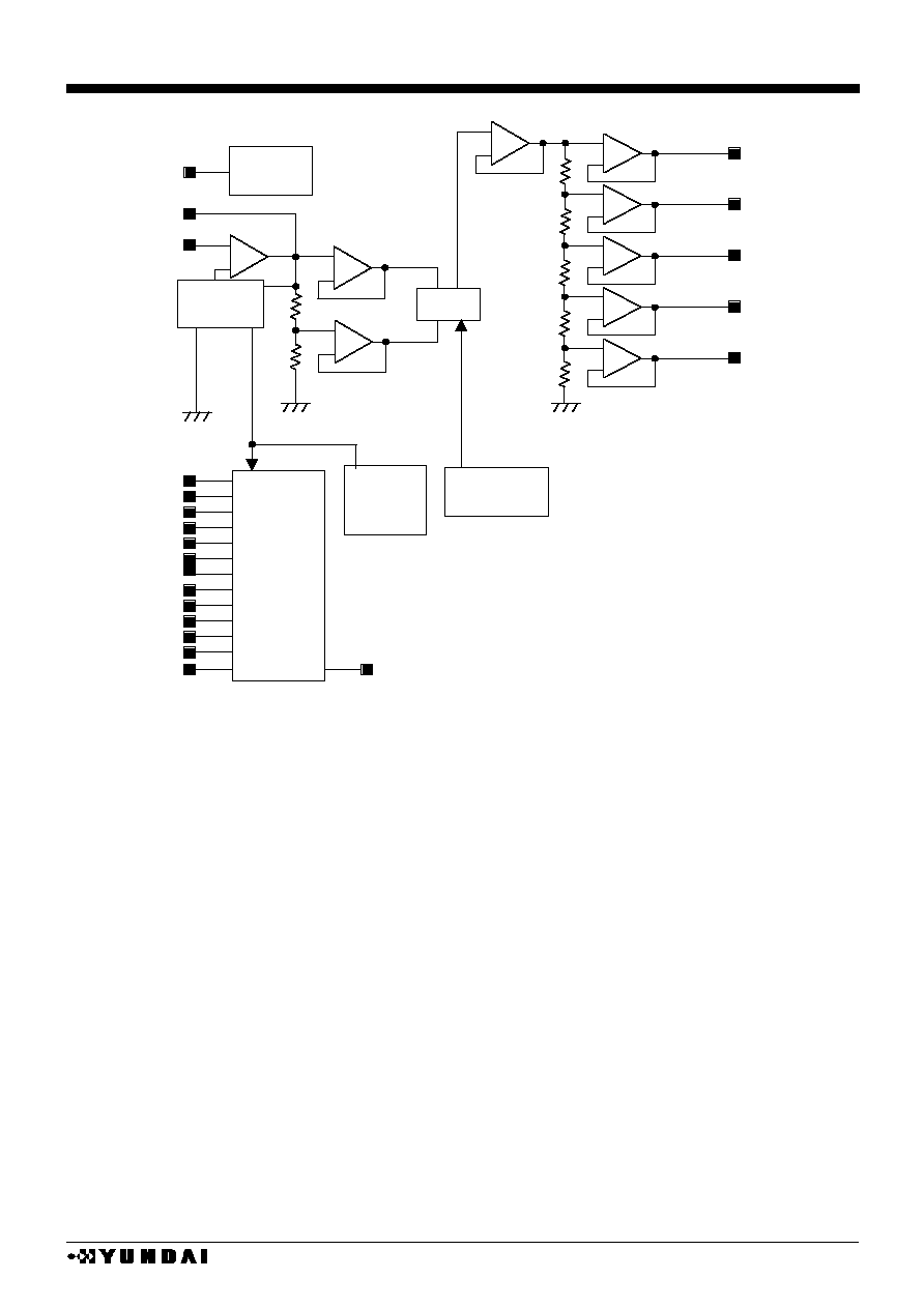
BLOCK DIAGRAM
V
SS
V
DD
V
LCD
, V
1
~V
4
V
OUT
V
BA
V
EE
INTERNAL BUS
!
"
#
$
%
"
&
'
$
(
(
$
)
0
0
)
"
'
1
2
3
4
5
6
7
3
8
4
9
1
2
3
4
@
A
A
9
4
B
B
A
4
5
6
A
4
9
C
@
A
A
9
4
B
B
A
4
5
6
A
4
9
D
E
F
G
H
I
P
D
I
Q
I
R
I
S
T
D
D
R
I
S
U
V
W
X
Y
X
`
Y
T
a
b
a
b
W
U
c
E
Q
E
d
e
f
D
I
Q
I
R
I
S
T
G
g
R
I
S
U
V
W
X
Y
W
Y
T
a
b
a
b
W
U
c
E
Q
0
$
h
#
)
h
'
CLK
'
FR
FLM
CL
#
(
$
h
A
2
B
i
1
@
p
B
8
@
9
8
1
2
3
4
9
4
q
2
B
8
4
9
5
RS
P/S SEL68
CS
WR
RD
TEST
RES
M/S
r
s
t
u
v
w
x
y
r
x
C
1
-
C
1
+
C
2
+
C
2
-
V
REF
C
3
+
C
3
-
C
4
+
C
4
-
SE
G
S
A
0
SE
G
S
B
0
SE
G
S
C
0
SE
G
A
0
SE
G
B
0
SE
G
C
0
SE
G
A
127
SE
G
B
127
SE
G
C
127
SE
G
S
A
2
SE
G
S
B
2
SE
G
S
C
2
C
O
M
I
0
C
O
M
0
C
O
M
79
C
O
M
I
1
0
"
"
'
$
)
#
$
#
$
'
"
'
"
"
'
#
$
'
0
$
'
C
@
A
A
9
4
B
B
9
4
q
2
B
8
4
9
C
@
A
A
9
4
B
B
5
6
7
3
8
4
9
!
"
#
)
'
!
"
0
$
'
"
(
$
)
'
"
#
%
#
)
'
$
)
'
#
'
$
)
#
OSC
1
SE
G
S
A
3
SE
G
S
B
3
SE
G
S
C
3
SE
G
S
A
1
SE
G
S
B
1
SE
G
S
C
1
C
5
+
C
5
-
C
6
+
C
6
-
0
$
'
"
#
)
'
#
$
"
'
D
7
D
4
/SPOL
D
6
D
15
D
14
D
13
D
12
D
5
D
11
D
10
D
9
D
8
D
3
/SMODE
D
0
/SCL
D
2
/EXCS
D
1
/SDA
2
6
7
4
9
V
SSH
OSC
2
V
REG
V
DDA
V
SSA
HM17CM256
- 9 -
s
POWER CIRCUIT BLOCK DIAGRAM
V
BA
V
REF
V
OUT
V
EE
'
C
1
+
C
1
-
C
2
+
C
2
-
C
3
+
C
3
-
C
4
+
C
4
-
C
5
+
C
5
-
C
6
+
C
6
-
E.V.R.
V
REG
)
#
h
'
"
0
0
)
"
'
h
'
"
0
#
)
h
$
)
'
%
'
'
$
)
0
0
$
'
#
'
$
#
h
(
'
'
$
)
0
0
$
'
V
1
V
2
V
3
V
4
V
LCD
0
"
$
)
#
)
'

HM17CM256
- 10 -
s
PIN DESCRIPTION 1
No.
NAME
I/O
FUNCTION
21,22,23,
39,40,41
V
DD
supply
Power pin for logic
27,28,29,
58,59,60
V
SS
supply
GND pin for logic
67,68,69,
88,89,90
V
SSH
supply
High voltage GND pin
31
V
DDA
supply
This pin is internally connected to V
DD
pin.
This pin is used when the voltage of each input pin is fixed to
V
DD
level.
caution) Do not use to main power pin.
17,18,19,
34,35,36
V
SSA
supply
This pin is internally connected to V
SS
pin.
This pin is used when the voltage of each input pin is fixed to
V
SS
level.
caution) Do not use to main power pin.
70,71,115,116
72,73
74,75
76,77
78,79
V
LCD
V
1
V
2
V
3
V
4
supply/O LCD driver supply voltage
�
LCD driver power supply port when external power supply
is used. When external power is used, voltages should
have following relations.
V
SS
<V
4
<V
3
<V
2
<V
1
<V
LCD
�
V
LCD
, V
1
~V
4
voltages are generated by voltage booster at
master mode operation under power circuit ON.
�
When internal power supply is used, capacitors must be
connected between V
LCD
, V
1
~V
4
and V
SS
.
91,92
93,94
C
1
+
C
1
-
O
Capacitor connection pin for voltage converter
95,96
97,98
C
2
+
C
2
-
O
Capacitor connection pin for voltage converter
99,100
101,102
C
3
+
C
3
-
O
Capacitor connection pin for voltage converter
103,104
105,106
C
4
+
C
4
-
O
Capacitor connection pin for voltage converter
107,108
109,110
C
5
+
C
5
-
O
Capacitor connection pin for voltage converter
111,112
113,114
C
6
+
C
6
-
O
Capacitor connection pin for voltage converter
82,83
V
BA
O
Reference voltage output pin for voltage regulating.
84
V
REF
I
Reference voltage input pin for voltage regulating.
85,86,87
V
EE
supply Voltage supply pin for boosted voltage generation.
V
DD
level at normal status.
117,118
V
OUT
supply/O Internal DC/DC converter output pin.
80,81
V
REG
O
Voltage regulator output pin.
24
RES
I
Reset pin
Reset when RES= "L"

HM17CM256
- 11 -
s
PIN DESCRIPTION 2
No.
NAME
I/O
FUNCTION
42
D
0
/SCL
I/O
43
D
1
/SDA
I/O
44
D
2
/EXCS
I/O
45
D
3
/SMODE
I/O
46
D
4
/SPOL
I/O
47,48,49
D
5
,D
6
,D
7
I/O
�
When parallel interface is selected (P/S="H"), data line is
connected to MPU data bus with 8bit bi-directional bus
�
When serial interface is selected (P/S="L"),
D
0
and D
1
(SCL, SDA) are used as serial interface pins
and various sets are taken by serial interface use mode of
D
2
, D
3
, D
4
.
SDA : serial data input pin
SCL : data transfer clock
EXCS : extension chip selection I/O pin
SMODE : serial transfer mode setting input pin
SPOL : RS polarity selection pin when 3 line serial interface is
selected.
SDA data is shifted at the rising edge of SCL
Internal serial/parallel conversion into 8-bit data occurs at the
rising edge of 8
th
clock of SCL.
Set to "L" after data transfer or during non-access time
50,51,52,53
54,55,56,57
D
8
,D
9
,D
10
,D
11
,
D
12
,D
13
,D
14
,D
15
I/O
Connect to data bus to MPU with 8bit bi-directional bus.
Used as MSB 8bit data bus in the 16bit data RAM transfer
mode
Set to "L" or "H" when not used.
25
CS
I
Chip selection pin.
Data in-out is possible when CS = "L".
Input data selection pin.
Distinguish bus data from CPU whether instruction or display
data.
RS
H
L
class
instruction
display data
26
RS
I
38
RD (E)
I
<80 series CPU interface (P/S="H",SEL68="L")>
RD signal connection port of 80 series CPU.
Data bus goes to output state at RD = "L".
<68 series CPU interface (P/S="H",SEL68="H")>
Enable signal connection port of 68 series CPU.
Active status when this signal is at "H".
<80 series CPU interface (P/S="H",SEL68="L")>
WR signal connection port of 80 series CPU.
Active at "L" and data bus signal is taken at the rising edge
of WR.
<68 series CPU interface (P/S="H",SEL68="H")>
Read write control signal , R/W connection port of 68-
series MPU.
R/W
H
L
status
read
write
37
WR (R/W)
I
HM17CM256
- 12 -
s
PIN DESCRIPTION 3
No.
NAME
I/O
FUNCTION
CPU interface selection port
SEL68
H
L
status
68 series
80 series
33
SEL68
I
Serial / parallel interface selection port
P/S
chip
select
data/
command
data
read/
write
serial clock
H
CS
RS
D
0
~D
7
RD, WR
-
L
CS
RS
SDA(D
1
)
write only
SCL (D
0
)
32
P/S
I
P/S = "L" :serial interface selection ,D15~D5 goes to Hi-Z
state. Fix RD, WR to "H" or "L".
20
TEST
I
Test port.
Fix to "L".
Latching signal pin of display data.
Display line counter is counted up at the rising edge and LCD
driving signal is generated at the falling edge
M/S
status
CL
H
master
output
L
slave
input
61
CL
I/O
LCD synchronous signal (first line marker) I/O pin.
Display start address is loaded in the display line counter at
FLM = "H".
M/S
status
FLM
H
master
output
L
slave
input
62
FLM
I/O
Alternated display signal of LCD driver output I/O pin.
M/S
status
FR
H
master
output
L
slave
input
63
FR
I/O
Master / slave mode selection pin
M/S
mode
oscillator Power supply
H
master
enable
enable
L
slave
disable
disable
30
M/S
I
Fix to "H" or "L" according to operating mode.
HM17CM256
- 13 -
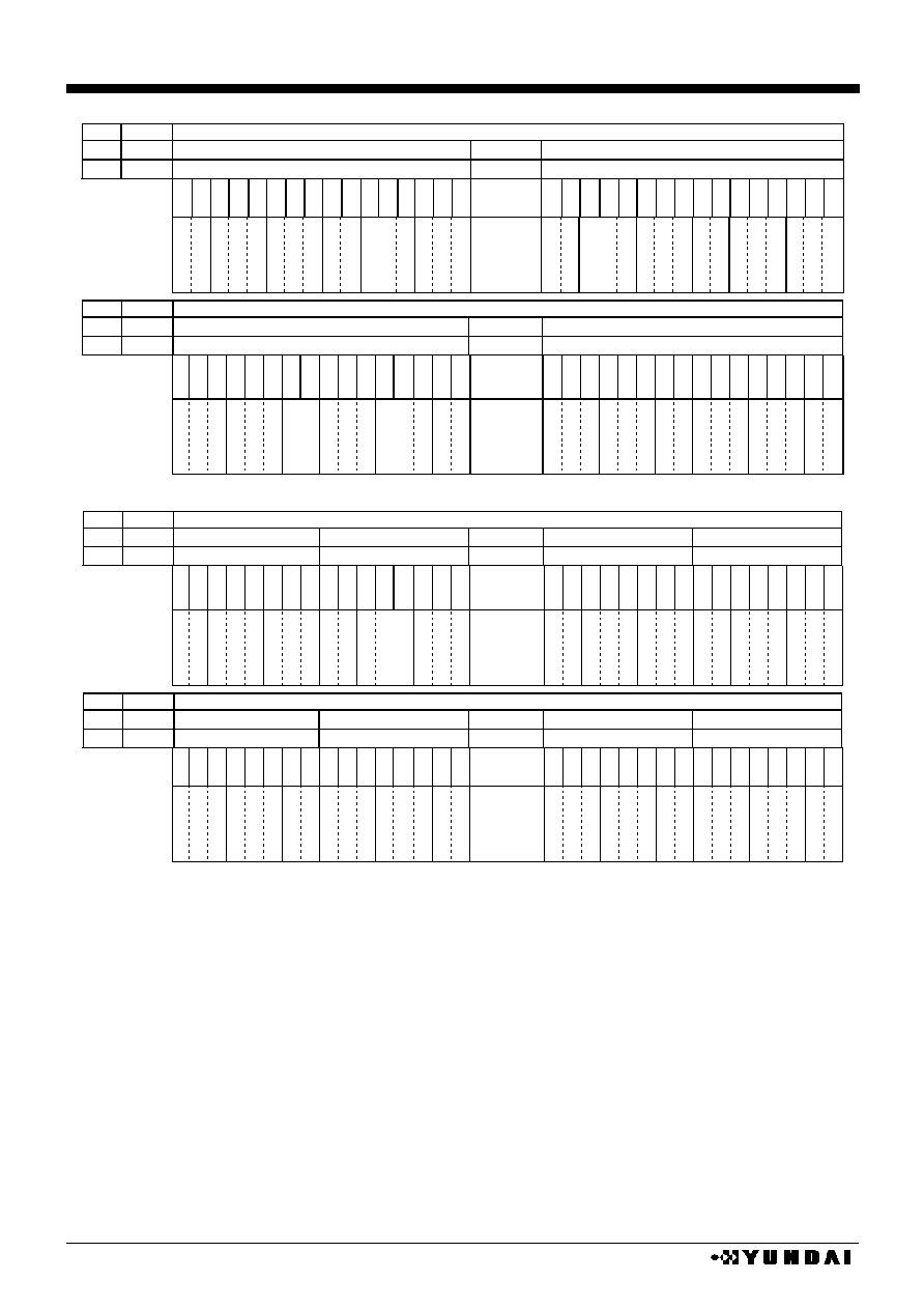
PIN DESCRIPTION 4
No.
NAME
I/O
FUNCTION
Segment drive port
Segment output from display RAM data
mode
Non-lighted
lighted
Normal
0
1
Reverse
1
0
The output level is selected among V
LCD
, V
2
, V
3
, V
SS
by the
combination of FR signal and RAM data
(B/W mode)
FR signal
display RAM data
Normal mode
V
2
V
LCD
V
3
V
SS
Reverse mode
V
LCD
V
2
V
SS
V
3
174~557
SEGA
0
~SEGA
127
,
SEGB
0
~SEGB
127
,
SEGC
0
~SEGC
127
O
164~169,
562~567
SEGSA
0
~SEGSA
3
,
SEGSB
0
~SEGSB
3
,
SEGSC
0
~SEGSC
3
O
Dummy segment driver output
Located at both side of segment drivers, used for edge
display.
Common driver output
The output level is selected among V
LCD
, V
1
, V
4
and V
SS
by
the combination of FR and scan data.
data
FR
Output level
H
H
V
SS
L
H
V
1
H
L
V
LCD
L
L
V
4
162~137,
132~119,
568~594,
3~15
COM
0
~COM
79
O
163
COMI
0
O
Common drive output for icon display
16
COMI
1
O
Common drive output for icon display
65,
66
OSC
1
,
OSC
2
I
O
External reference clock input pin
Open when using internal oscillator clock or used as slave
device.
In this case, OSC
1
goes to V
SS
level.
Connect external oscillating source to OSC
1
port or connect
resistor between OSC
1
and OSC
2
when using external
oscillator.
Input / output pin for display timing clock
Output clock from master device is applied to slave chip
through CLK pin when used as master / slave mode.
M/S
mode
CLK
H
master
output
L
slave
input*
64
CLK
I/O
*input from master chip's CLK output
(port No. 1,2,133,134,135,136,170,171,172,173,558,559,560,561,595,596 is dummy port.)
HM17CM256
- 14 -
s
FUNCTION DESCRIPTION
(1) CPU interface
(1-1) Selection of interface type
HM17CM256 receives data through 8 bit parallel I/O(D
0
~D
7
)
16 bit parallel I/O(D
0
~D
15
) or
divided into serial data input (SDA, SCL). Parallel or serial selection is decided by P/S pin setting.
Parallel or serial selection is possible as following table.
Reading out from internal register or RAM is not possible at serial interface mode.
TABLE
P/S
Type
CS
RS
RD
WR
SEL68
SDA
SCL
data
H
Parallel input
CS
RS
RD
WR
SEL68
D
0
~D
7
(D
0
~D
15
)
L
Serial input
CS
RS
-
-
-
SDA
SCL
-
caution 1) "-" mark item : Fix to "H" or "L"
(1-2) Parallel input
In the parallel interface mode selected by P/S port, parallel data is transferred from the
8bit/16bit MPU through data bus. SEL68 port setting makes 80-series or 68-series interface
selection
TABLE
SEL68
CPU type
CS
RS
RD
WR
data
H
68 series CPU
CS
RS
E
R/W
D
0
~D
7
(D
0
~D
15
)
L
80 series CPU
CS
RS
RD
WR
D
0
~D
7
(D
0
~D
15
)
(1-3) Data identification
Combinations of RS, RD, and WR signals identify contents of 8bit data bus.
TABLE
68 series
80 series
RS
R/W
RD
WR
FUNCTION
1
1
0
1
Read out from internal register
1
0
1
0
Write in to internal register
0
1
0
1
Read display data
0
0
1
0
Write display data
(1-4) Serial interface
2 types of serial interface (3 line type mode, 4 line type mode) are available by selecting
SMODE pin.
TABEL
SMODE
Serial interface mode
H
3 line type
L
4 line type
HM17CM256
- 15 -
(1-5) 4 line type serial interface
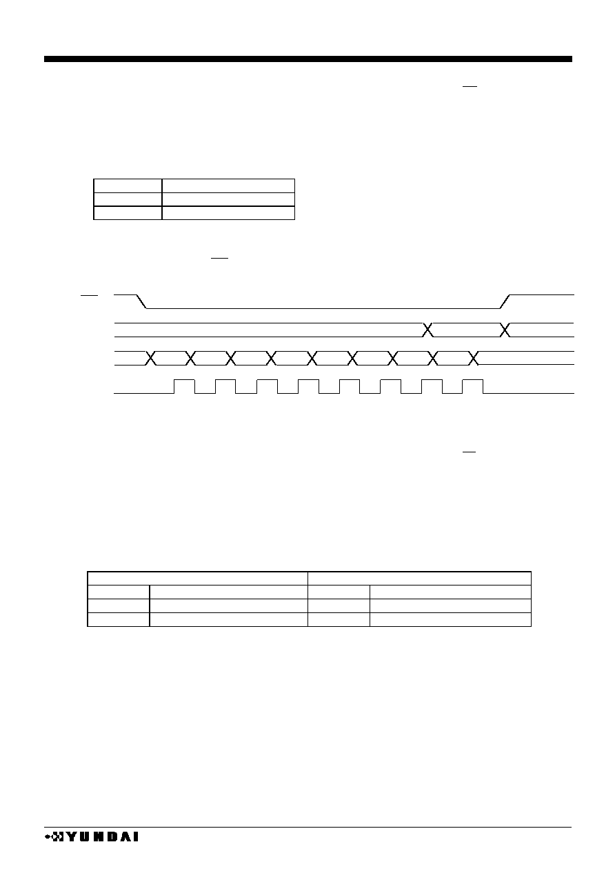
4 line serial interface by SDA and SCL is possible at chip selection state (CS="L")
When chip is not selected, internal shift register and counter are reset to initial value.
Serial input data from SDA are latched at the rising edge of serial clock (SCL) in the sequence
of D
7
,
, D
1
, D
0
and converted into 8-bit parallel data at the rising edge of 8th serial clock.
Serial data (SDA) are identified to display data or command by RS input.
TABLE
RS
Data contents
H
command
L
Display data
Make serial clock (SCL) "L" at the non-access period and after 8bit data transfer.
SDA and SCL signals are sensitive to external noise. To prevent mal-function, chip selector
state should be released (CS = "H") after 8bit data transfer as shown in the following figure.
4 line serial interface
(1-6) 3 line type serial interface
3-line serial interface by SDA and SCL is possible at chip selection state (CS="L")
When chip is not selected, internal shift register and counter are reset to initial value.
Input data from SDA are latched at the rising edge of serial clock (SCL) in the sequence of RS,
D
7
, ,D
1
, D
0
, and converted to 8bit parallel data and handled at the rising edge of 9th serial
clock.
Serial data (SDA) are identified to display data or command by RS bit data at the rising of first
serial clock (SCL) and state of command data bit polarity shift pin (SPOL).
TABLE
SPOL=L
SPOL=H
RS
Data identify
RS
Data identify
L
Display data
L
command
H
command
H
Display data
D
7
D
6
D
5
D
4
D
3
D
2
D
1
D
0
VALID
1
2
3
4
5
6
7
8
CS
RS
SDA
SCL

HM17CM256
- 16 -
Serial clock (SCL) should go to "L" at the non-access period and after 9bit data transfer.
SDA and SCL signals are sensitive to external noise. To prevent miss operation chip
selector state should be released (CS = "H") after 9bit data transfer as shown in the following
figure.
3line serial interface
(1-7) One systematization of CS when serial interface is selected
In the multi-chip operation (master/slave) mode with serial I/F connection, one CS signal
controls two chips to reduce control signal.
Connect extended chip selection port (EXCS) of master chip to EXCS port ( input at slave
device and output at master device mode ) of slave chip.
When EXCS is "L", master chip cannot accept command except for EXCS control; at this
point, only slave chip can be controlled.
Slave device control is possible when CS = "L" period within EXCS = "L" state.
RS
D
7
D
6
D
5
D
4
D
3
D
2
D
1
1
2
3
4
5
6
7
8
CS
SDA
SCL
D
0
9
SDA
CS
SCL
RS
M/S
P/S
SMODE
SPOL
EXCS
(MASTER)
SDA
CS
SCL
RS
M/S
P/S
SMODE
SPOL
EXCS
(SLAVE)
CS
SDA
SCL
RS
EXCS: expand CS signal ( input port )
Master device : output port
Slave device : input port
(input port)
P/S=0: serial I/F
P/S=1: parallel I/F
P/S: parallel . serial selection port
(input port)
M/S=0: slave operation
M/S=1: master operation
M/S: master . slave selection port
(input port)
SMODE=0: 4 line serial I/F
SMODE=1: 3 line serial I/F
SMODE: serial I/Fmode selection port
(input port)
Access display RAM at SPOL=0:RS=0
Access display RAM at SPOL=1:RS=1
SPOL:command data bit polarity selection port
At 3 line serial I/F mode

HM17CM256
- 17 -
(2) DDRAM and internal register access
DDRAM and internal register are accessed by data bus D
0
~D
7
(D
0
~D
15
), chip select pin (CS),
DDRAM / register select pin (RS), read / write control pin (RD) or WR pin.
When CS="H", it is in non-selective state and DDRAM and internal register access is impossible.
During access, Set CS="L".
Access selection to DDRAM or internal register is controlled by RS input.
TABLE
RS
Data contents
L
Display RAM data
H
Internal command register
Write process starts after address setting and then the data on the 8bit data bus D
0
~D
7
or 16bit
data bus D
0
~D
15
will be written in by CPU. The data is written at the rising edge of WR (80 series) or
falling edge of E (68 series).
Internally, bus holder data is processed to data bus and data are written to bus holder from CPU
until next cycle.
After address setting, data of assigned address are read at the 1st and 3rd clock, which means it
needs dummy read at the 2nd clock.
There are rules at reading data out of display RAM, after address setting, the data of assigned
address is shown directly after the end of the read command, so pay attention that assigned data is
available at 2nd timing step.
In other words, 1 cycle dummy read is needed after address setting and write cycle.
DATA WRITE IN OPERATION
DATA READ OUT OPERATION
caution) When 16 bit mode, do write in and read out by 16 bit not only RAM access but also command
setting.
n
n+2
D
0
~D
15
WR
BUS HOLDER
WR
n
n+1
n+2
n+3
n+4
n+1
n+3
n+4
D
0
~D
7
(D
0
~D
15
)
RD
n
n
n+1
n+2
WR
address set
n
dummy
read
data read
n address
data read
n+1 address
data read
n+2 address

HM17CM256
- 18 -
(3) Read out of internal register
Read out is possible not only from DDRAM, but also from the internal register. Addresses for
read (0~F
H
) are allocated in each register.
Read out is executed after writing read-out register address to internal register.
Internal register read out sequence
When register is read out, upper 4 bit data are "1111".
Non-used bits of active registers are "0".
When non-used registers are read out, upper 4 bits are "1111" and lower 4 bits are "0000".
(4) 16 bit data access to DDRAM
It is possible to write in DDRAM by 16-bits access with the data of 16 bits data bus D
0
~D
15
.
16 bits data access mode is possible by setting the value of WLS register to "1".
TABEL
WLS
Acess mode
L
8 bit
H
16 bit
Each command should be set to 8-bits(D
0
~D
7
) as well as to 16-bit access mode.
16-bit access is available at display RAM access.
(5) Display start line register
When displaying the DDRAM data, it is the contents of Y address register that is corresponding to
display start line.
The data of Y address is displayed on the display start line depending on the value of the shift
command register and the display start line register.
The data of this register are preset to the display line counter per FLM signal transition.
Line counter is counted up in synchronization with CL input and generates line address that read
out 384bit data from DDRAM to LCD driver circuit.
D
0
~D
7
M
N
WR
Address set
for
register read
Internal
register read
Address set
for
register read
Internal
register read
m
n
RD
RE register set:100
Internal register read address set
set RE of register to be read out
Internal register read

HM17CM256
- 19 -
(6) DDRAM addressing
This IC includes display memory Bit mapped that is composed of 1024 bit of X direction
(8bit
�
128) and 82bit of Y direction.
In gray mode, neighboring 3-bit data or 2-bit data are displayed by segment driver with 8 grays or
4 grays, respectively.
3 outputs of segment driver compose 1 pixel of RGB and 128
�
82 pixels are displayed with 256
color (8gray
�
8gray
�
4gray).
Address area of X direction is varied according to accessed data length. The area of X direction
is 0
H
~7F
H
at 8bit access mode and 0
H
~3F
H
at 16bit access mode.
�
8BIT access
X-address
0
H
1
H
7E
H
7F
H
0
H
8bit 8bit
8bit 8bit
Y-address
51
H
8bit 8bit
8bit 8bit
�
16 BIT access
X-address
0
H
3F
H
0
H
16bit
16bit
Y-address
51
H
16bit
16bit
In the Black & white mode, the MSBs of 3 bit and 2 bit corresponding with RGB are used to
display data. And so, 128x82 dot gray display or 384 x 82 B/W mode display is possible.
Display RAM is accessed with X address and Y address from CPU by 8 bit or 16 bit unit.
X address and Y address can be increased automatically by setting status of control register.
The address is increased per every read and write of display RAM by CPU. ( Please see detail
description at command function.)
X direction is selected by X address and Y direction is selected by Y address. Please do not set
the address on non-effective area and it is forbidden to set address on outside area in each case.
384bit display data of Y direction are read out to display latch at rising edge of CL signal per 1 line
cycle and this data comes out from display latch at falling edge of CL signal.
Display start line address register is preset to line counter at "H" state of FLM signal which changes
per one frame cycle and the address is counted up with synchronized CL input.
Display line address counter is synchronized by timing signals of LCD driver, and it operates
independently with X, Y address counters.

HM17CM256
- 20 -
(7) Window address assign of display RAM
This IC can be accessed to display RAM by window area designation in addition to access to
display RAM designated by X and Y address.
Through address space of all display address, specific area of RAM can be accessed by
designated two points.
The start point of two point addresses is assigned by normal X address and Y address register and
the end point of them is done by X end address and Y end address register value. Designated
inner addresses depend on WLS bit.
Read modified write action can be taken by AIM="1".
In case of using window area accessing mode, you must set start point X address, Y address in
sequence and end point X address, Y address in sequence after executing Win command (WIN="1",
auto increase mode AXI="1", AYI="1") and then access to Display RAM.
And set start point and end point not to be designated to access the outside of available address
area. Address set value should be taken to set AX
EX ( end point of X address ) and AY
EY
( end point of Y address ).
X direction
(X, Y)
address designation
end address designation
Window display area
(X, Y)
All display RAM area
(8) display RAM data and LCD
Display RAM data related with one dot of LCD is dependent on REV register. Normal display and
reverse display by REV register are set up as follows.
TABLE
REV
Display
RAM data
0
L
normal
1
0
H
reverse
1
(9) Segment display output order/reverse set up
The order of display outputs, SEGA
0
, SEGB
0
, SEGC
0
to SEGA
127
, SEGB
127
, and can be reversed
by reversing access to display RAM from MPU by using REF register, lessen the limitation in placing
IC when assembling an LCD panel module.
Y
d
i
r
ec
t
i
on

HM17CM256
- 21 -
(10) Relation between Display RAM and address
�
RAM address and bitmap
COLOR / 16 BIT MODE
REF SWAP
X address / bit / segment assign
0
0
X=00
H
X=3F
H
1
1
X=3F
H
X=00
H
D
0
D
1
D
2
D
3
D
4
D
5
D
6
D
7
D
8
D
9
D
10
D
1
1
D
12
D
13
D
14
D
15
d
d
D
0
D
1
D
2
D
3
D
4
D
5
D
6
D
7
D
8
D
9
D
10
D
1
1
D
12
D
13
D
14
D
15
pa
l
e
tt
e
A
pa
l
e
tt
e
B
pa
l
e
tt
e
C
pa
l
e
tt
e
A
pa
l
e
tt
e
B
pa
l
e
tt
e
C
d
d
pa
l
e
tt
e
A
pa
l
e
tt
e
B
pa
l
e
tt
e
C
pa
l
e
tt
e
A
pa
l
e
tt
e
B
pa
l
e
tt
e
C
SE
G
A
0
SE
G
B
0
SE
G
C
0
SE
G
A
1
SE
G
B
1
SE
G
C
1
d
d
SE
G
A
126
SE
G
B
126
SE
G
C
126
SE
G
A
127
SE
G
B
127
SE
G
C
127
REF SWAP
X address / bit / segment assign
0
1
X=00
H
e
e
X=3F
H
1
0
X=3F
H
e
e
X=00
H
D
15
D
14
D
13
D
12
D
1
1
D
10
D
9
D
8
D
7
D
6
D
5
D
4
D
3
D
2
D
1
D
0
d
d
D
15
D
14
D
13
D
12
D
1
1
D
10
D
9
D
8
D
7
D
6
D
5
D
4
D
3
D
2
D
1
D
0
pa
l
e
tt
e
C
pa
l
e
tt
e
B
pa
l
e
tt
e
A
pa
l
e
tt
e
C
pa
l
e
tt
e
B
pa
l
e
tt
e
A
d
d
pa
l
e
tt
e
C
pa
l
e
tt
e
B
pa
l
e
tt
e
A
pa
l
e
tt
e
C
pa
l
e
tt
e
B
pa
l
e
tt
e
A
SE
G
A
0
SE
G
B
0
SE
G
C
0
SE
G
A
1
SE
G
B
1
SE
G
C
1
d
d
SE
G
A
126
SE
G
B
126
SE
G
C
126
SE
G
A
127
SE
G
B
127
SE
G
C
127
COLOR / 8 BIT MODE
REF SWAP
X address / bit / segment assign
0
0
X=00
H
X=01
H
e
e
X=7E
H
X=7F
H
1
1
X=7F
H
X=7E
H
e
e
X=01
H
X=00
H
D
0
D
1
D
2
D
3
D
4
D
5
D
6
D
7
D
0
D
1
D
2
D
3
D
4
D
5
D
6
D
7
d
d
D
0
D
1
D
2
D
3
D
4
D
5
D
6
D
7
D
0
D
1
D
2
D
3
D
4
D
5
D
6
D
7
pa
l
e
tt
e
A
pa
l
e
tt
e
B
pa
l
e
tt
e
C
pa
l
e
tt
e
A
pa
l
e
tt
e
B
pa
l
e
tt
e
C
d
d
pa
l
e
tt
e
A
pa
l
e
tt
e
B
pa
l
e
tt
e
C
pa
l
e
tt
e
A
pa
l
e
tt
e
B
pa
l
e
tt
e
C
SE
G
A
0
SE
G
B
0
SE
G
C
0
SE
G
A
1
SE
G
B
1
SE
G
C
1
d
d
SE
G
A
126
SE
G
B
126
SE
G
C
126
SE
G
A
127
SE
G
B
127
SE
G
C
127
REF SWAP
X address / bit / segment assign
0
1
X=00
H
X=01
H
e
e
X=7E
H
X=7F
H
1
0
X=7F
H
X=7E
H
e
e
X=01
H
X=00
H
D
7
D
6
D
5
D
4
D
3
D
2
D
1
D
0
D
7
D
6
D
5
D
4
D
3
D
2
D
1
D
0
d
d
D
7
D
6
D
5
D
4
D
3
D
2
D
1
D
0
D
7
D
6
D
5
D
4
D
3
D
2
D
1
D
0
pa
l
e
tt
e
C
pa
l
e
tt
e
B
pa
l
e
tt
e
A
pa
l
e
tt
e
C
pa
l
e
tt
e
B
pa
l
e
tt
e
A
d
d
pa
l
e
tt
e
C
pa
l
e
tt
e
B
pa
l
e
tt
e
A
pa
l
e
tt
e
C
pa
l
e
tt
e
B
pa
l
e
tt
e
A
SE
G
A
0
SE
G
B
0
SE
G
C
0
SE
G
A
1
SE
G
B
1
SE
G
C
1
d
d
SE
G
A
126
SE
G
B
126
SE
G
C
126
SE
G
A
127
SE
G
B
127
SE
G
C
127
HM17CM256
- 22 -
BLACK & WHITE / 16 BIT MODE
REF SWAP
X address / bit / segment assign
0
0
X=00
H
f
f
X=3F
H
1
1
X=3F
H
f
f
X=00
H
D
0
D
1
D
2
D
3
D
4
D
5
D
6
D
7
D
8
D
9
D
10
D
1
1
D
12
D
13
D
14
D
15
g
g
D
0
D
1
D
2
D
3
D
4
D
5
D
6
D
7
D
8
D
9
D
10
D
1
1
D
12
D
13
D
14
D
15
SE
G
A
0
SE
G
B
0
SE
G
C
0
SE
G
A
1
SE
G
B
1
SE
G
C
1
g
g
SE
G
A
126
SE
G
B
126
SE
G
C
126
SE
G
A
127
SE
G
B
127
SE
G
C
127
REF SWAP
X address / bit / segment assign
0
1
X=00
H
f
f
X=3F
H
1
0
X=3F
H
f
f
X=00
H
D
15
D
14
D
13
D
12
D
1
1
D
10
D
9
D
8
D
7
D
6
D
5
D
4
D
3
D
2
D
1
D
0
g
g
D
15
D
14
D
13
D
12
D
1
1
D
10
D
9
D
8
D
7
D
6
D
5
D
4
D
3
D
2
D
1
D
0
SE
G
A
0
SE
G
B
0
SE
G
C
0
SE
G
A
1
SE
G
B
1
SE
G
C
1
g
g
SE
G
A
126
SE
G
B
126
SE
G
C
126
SE
G
A
127
SE
G
B
127
SE
G
C
127
BLACK & WHITE / 8 BIT MODE
REF SWAP
X address / bit / segment assign
0
0
X=00
H
X=01
H
f
f
X=7E
H
X=7F
H
1
1
X=7F
H
X=7E
H
f
f
X=01
H
X=00
H
D
0
D
1
D
2
D
3
D
4
D
5
D
6
D
7
D
0
D
1
D
2
D
3
D
4
D
5
D
6
D
7
g
g
D
0
D
1
D
2
D
3
D
4
D
5
D
6
D
7
D
0
D
1
D
2
D
3
D
4
D
5
D
6
D
7
SE
G
A
0
SE
G
B
0
SE
G
C
0
SE
G
A
1
SE
G
B
1
SE
G
C
1
g
g
SE
G
A
126
SE
G
B
126
S
E
G
C
126
SE
G
A
127
SE
G
B
127
SE
G
C
127
REF SWAP
X address / bit / segment assign
0
1
X=00
H
X=01
H
f
f
X=7E
H
X=7F
H
1
0
X=7F
H
X=7E
H
f
f
X=01
H
X=00
H
D
7
D
6
D
5
D
4
D
3
D
2
D
1
D
0
D
7
D
6
D
5
D
4
D
3
D
2
D
1
D
0
g
g
D
7
D
6
D
5
D
4
D
3
D
2
D
1
D
0
D
7
D
6
D
5
D
4
D
3
D
2
D
1
D
0
SE
G
A
0
SE
G
B
0
SE
G
C
0
SE
G
A
1
SE
G
B
1
SE
G
C
1
g
g
SE
G
A
126
SE
G
B
126
SE
G
C
126
SE
G
A
127
SE
G
B
127
SE
G
C
127
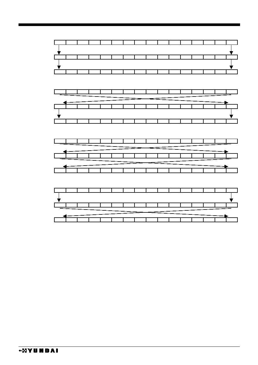
HM17CM256
- 23 -
�
WRITE IN / READ IN BITMAP ( 16 BIT MODE )
REF=0, SWAP=0
WRITE IN DATA D
0
D
1
D
2
D
3
D
4
D
5
D
6
D
7
D
8
D
9
D
10
D
11
D
12
D
13
D
14
D
15
SEGMENT DATA SEG
0
SEG
1
SEG
2
SEG
3
SEG
4
SEG
5
SEG
6
SEG
7
SEG
8
SEG
9
SEG
10
SEG
11
SEG
12
SEG
13
SEG
14
SEG
15
READ IN DATA D
0
D
1
D
2
D
3
D
4
D
5
D
6
D
7
D
8
D
9
D
10
D
11
D
12
D
13
D
14
D
15
REF=0, SWAP=1
WRITE IN DATA D
0
D
1
D
2
D
3
D
4
D
5
D
6
D
7
D
8
D
9
D
10
D
11
D
12
D
13
D
14
D
15
SEGMENT DATA SEG
0
SEG
1
SEG
2
SEG
3
SEG
4
SEG
5
SEG
6
SEG
7
SEG
8
SEG
9
SEG
10
SEG
11
SEG
12
SEG
13
SEG
14
SEG
15
READ IN DATA D
0
D
1
D
2
D
3
D
4
D
5
D
6
D
7
D
8
D
9
D
10
D
11
D
12
D
13
D
14
D
15
REF=1, SWAP=0
WRITE IN DATA D
0
D
1
D
2
D
3
D
4
D
5
D
6
D
7
D
8
D
9
D
10
D
11
D
12
D
13
D
14
D
15
SEGMENT DATA SEG
0
SEG
1
SEG
2
SEG
3
SEG
4
SEG
5
SEG
6
SEG
7
SEG
8
SEG
9
SEG
10
SEG
11
SEG
12
SEG
13
SEG
14
SEG
15
READ IN DATA D
0
D
1
D
2
D
3
D
4
D
5
D
6
D
7
D
8
D
9
D
10
D
11
D
12
D
13
D
14
D
15
REF=1, SWAP=1
WRITE IN DATA D
0
D
1
D
2
D
3
D
4
D
5
D
6
D
7
D
8
D
9
D
10
D
11
D
12
D
13
D
14
D
15
SEGMENT DATA SEG
0
SEG
1
SEG
2
SEG
3
SEG
4
SEG
5
SEG
6
SEG
7
SEG
8
SEG
9
SEG
10
SEG
11
SEG
12
SEG
13
SEG
14
SEG
15
READ IN DATA D
0
D
1
D
2
D
3
D
4
D
5
D
6
D
7
D
8
D
9
D
10
D
11
D
12
D
13
D
14
D
15

HM17CM256
- 24 -
�
READ OUT AFTER WROTE IN DATA ( 16 BIT MODE )
REF=0, SWAP=0
D
15
D
0
WRITE IN DATA 1
1
1
0
0
1
0
0
1
1
1
1
0
0
1
0 (E4F2
H
)
D
15
D
0
READ IN DATA 1
1
1
0
0
1
0
0
1
1
1
1
0
0
1
0 (E4F2
H
)
REF=0, SWAP=1
D
15
D
0
WRITE IN DATA 1
1
1
0
0
1
0
0
1
1
1
1
0
0
1
0 (E4F2
H
)
D
15
D
0
READ IN DATA 0
1
0
0
1
1
1
1
0
0
1
0
0
1
1
1 (4F27
H
)
REF=1, SWAP=0
D
15
D
0
WRITE IN DATA 1
1
1
0
0
1
0
0
1
1
1
1
0
0
1
0 (E4F2
H
)
D
15
D
0
READ IN DATA 1
1
1
0
0
1
0
0
1
1
1
1
0
0
1
0 (E4F2
H
)
REF=1, SWAP=1
D
15
D
0
WRITE IN DATA 1
1
1
0
0
1
0
0
1
1
1
1
0
0
1
0 (E4F2
H
)
D
15
D
0
READ IN DATA 0
1
0
0
1
1
1
1
0
0
1
0
0
1
1
1 (4F27
H
)

HM17CM256
- 25 -
�
WRITE IN / READ IN BITMAP ( 8 BIT MODE )
REF=0, SWAP=0
WRITE IN DATA D
0
D
1
D
2
D
3
D
4
D
5
D
6
D
7
SEGMENT DATA SEG
0
SEG
1
SEG
2
SEG
3
SEG
4
SEG
5
SEG
6
SEG
7
READ IN DATA D
0
D
1
D
2
D
3
D
4
D
5
D
6
D
7
REF=0, SWAP=1
WRITE IN DATA D
0
D
1
D
2
D
3
D
4
D
5
D
6
D
7
SEGMENT DATA SEG
0
SEG
1
SEG
2
SEG
3
SEG
4
SEG
5
SEG
6
SEG
7
READ IN DATA D
0
D
1
D
2
D
3
D
4
D
5
D
6
D
7
REF=1, SWAP=0
WRITE IN DATA D
0
D
1
D
2
D
3
D
4
D
5
D
6
D
7
SEGMENT DATA SEG
0
SEG
1
SEG
2
SEG
3
SEG
4
SEG
5
SEG
6
SEG
7
READ IN DATA D
0
D
1
D
2
D
3
D
4
D
5
D
6
D
7
REF=1, SWAP=1
WRITE IN DATA D
0
D
1
D
2
D
3
D
4
D
5
D
6
D
7
SEGMENT DATA SEG
0
SEG
1
SEG
2
SEG
3
SEG
4
SEG
5
SEG
6
SEG
7
READ IN DATA D
0
D
1
D
2
D
3
D
4
D
5
D
6
D
7

HM17CM256
- 26 -
�
READ OUT AFTER WROTE IN DATA ( 8 BIT MODE )
REF=0, SWAP=0
D
15
D
0
WRITE IN DATA 1
1
1
0
0
1
0
0
(E4
H
)
D
15
D
0
READ IN DATA 1
1
1
0
0
1
0
0
(E4
H
)
REF=0, SWAP=1
D
15
D
0
WRITE IN DATA 1
1
1
0
0
1
0
0
(E4
H
)
D
15
D
0
READ IN DATA 0
0
1
0
0
1
1
1
(27
H
)
REF=1, SWAP=0
D
15
D
0
WRITE IN DATA 1
1
1
0
0
1
0
0
(E4
H
)
D
15
D
0
READ IN DATA 1
1
1
0
0
1
0
0
(E4
H
)
REF=1, SWAP=1
D
15
D
0
WRITE IN DATA 1
1
1
0
0
1
0
0
(E4
H
)
D
15
D
0
READ IN DATA 0
0
1
0
0
1
1
1
(27
H
)
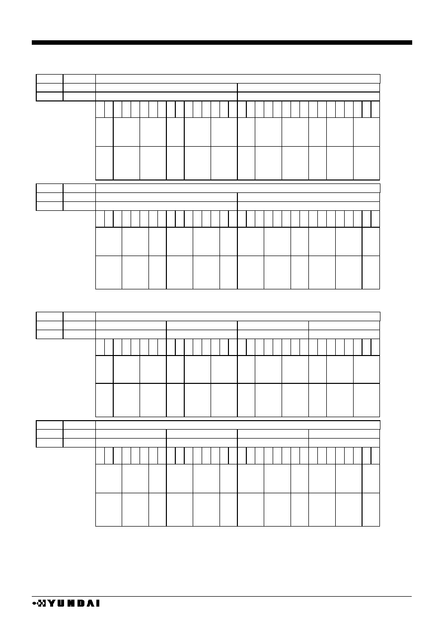
HM17CM256
- 27 -
�
DUMMY SEGMENT REGISTER ADDRESS AND BITMAP
COLOR / 16 BIT MODE
REF SWAP
X address / bit segment assign
0
0
X=00
H
X=01
H
1
1
X=01
H
X=00
H
D
0
D
1
D
2
D
3
D
4
D
5
D
6
D
7
D
8
D
9
D
10
D
1
1
D
12
D
13
D
14
D
15
D
0
D
1
D
2
D
3
D
4
D
5
D
6
D
7
D
8
D
9
D
10
D
1
1
D
12
D
13
D
14
D
15
P
a
l
e
tt
e
A
P
a
l
e
tt
e
B
P
a
l
e
tt
e
C
P
a
l
e
tt
e
A
P
a
l
e
tt
e
B
P
a
l
e
tt
e
C
P
a
l
e
tt
e
A
P
a
l
e
tt
e
B
P
a
l
e
tt
e
C
P
a
l
e
tt
e
A
P
a
l
e
tt
e
B
P
a
l
e
tt
e
C
SE
G
SA
0
SE
G
SB
0
SE
G
S
C
0
SE
G
SA
1
SE
G
SB
1
SE
G
S
C
1
SE
G
SA
2
SE
G
SB
2
SE
G
S
C
2
SE
G
SA
3
SE
G
SB
3
SE
G
S
C
3
REF SWAP
X address / bit segment assign
0
1
X=00
H
X=01
H
1
0
X=01
H
X=00
H
D
15
D
14
D
13
D
12
D
1
1
D
10
D
9
D
8
D
7
D
6
D
5
D
4
D
3
D
2
D
1
D
0
D
15
D
14
D
13
D
12
D
1
1
D
10
D
9
D
8
D
7
D
6
D
5
D
4
D
3
D
2
D
1
D
0
P
a
l
e
tt
e
C
P
a
l
e
tt
e
B
P
a
l
e
tt
e
A
P
a
l
e
tt
e
C
P
a
l
e
tt
e
B
P
a
l
e
tt
e
A
P
a
l
e
tt
e
C
P
a
l
e
tt
e
B
P
a
l
e
tt
e
A
P
a
l
e
tt
e
C
P
a
l
e
tt
e
B
P
a
l
e
tt
e
A
SE
G
SA
0
SE
G
SB
0
SE
G
S
C
0
SE
G
SA
1
SE
G
SB
1
SE
G
S
C
1
SE
G
SA
2
SE
G
SB
2
SE
G
S
C
2
SE
G
SA
3
SE
G
SB
3
SE
G
S
C
3
COLOR / 8 BIT MODE
REF SWAP
X address / bit segment assign
0
0
X=00
H
X=01
H
X=02
H
X=03
H
1
1
X=03
H
X=02
H
X=01
H
X=00
H
D
0
D
1
D
2
D
3
D
4
D
5
D
6
D
7
D
0
D
1
D
2
D
3
D
4
D
5
D
6
D
7
D
0
D
1
D
2
D
3
D
4
D
5
D
6
D
7
D
0
D
1
D
2
D
3
D
4
D
5
D
6
D
7
P
a
l
e
tt
e
A
P
a
l
e
tt
e
B
P
a
l
e
tt
e
C
P
a
l
e
tt
e
A
P
a
l
e
tt
e
B
P
a
l
e
tt
e
C
P
a
l
e
tt
e
A
P
a
l
e
tt
e
B
P
a
l
e
tt
e
C
P
a
l
e
tt
e
A
P
a
l
e
tt
e
B
P
a
l
e
tt
e
C
SE
G
SA
0
SE
G
SB
0
SE
G
S
C
0
SE
G
SA
1
SE
G
SB
1
SE
G
S
C
1
SE
G
SA
2
SE
G
SB
2
SE
G
S
C
2
SE
G
SA
3
SE
G
SB
3
SE
G
S
C
3
REF SWAP
X address / bit segment assign
0
1
X=00
H
X=01
H
X=02
H
X=03
H
1
0
X=03
H
X=02
H
X=01
H
X=00
H
D
7
D
6
D
5
D
4
D
3
D
2
D
1
D
0
D
7
D
6
D
5
D
4
D
3
D
2
D
1
D
0
D
7
D
6
D
5
D
4
D
3
D
2
D
1
D
0
D
7
D
6
D
5
D
4
D
3
D
2
D
1
D
0
P
a
l
e
tt
e
C
P
a
l
e
tt
e
B
P
a
l
e
tt
e
A
P
a
l
e
tt
e
C
P
a
l
e
tt
e
B
P
a
l
e
tt
e
A
P
a
l
e
tt
e
C
P
a
l
e
tt
e
B
P
a
l
e
tt
e
A
P
a
l
e
tt
e
C
P
a
l
e
tt
e
B
P
a
l
e
tt
e
A
SE
G
SA
0
SE
G
SB
0
SE
G
S
C
0
SE
G
SA
1
SE
G
SB
1
SE
G
S
C
1
SE
G
SA
2
SE
G
SB
2
SE
G
S
C
2
SE
G
SA
3
SE
G
SB
3
SE
G
S
C
3

HM17CM256
- 28 -
�
BLACK 7 WHITE / 16 BIT MODE
REF SWAP
X address / bit segment assign
0
0
X=00
H
X=01
H
1
1
X=01
H
X=00
H
D
0
D
1
D
2
D
3
D
4
D
5
D
6
D
7
D
8
D
9
D
10
D
1
1
D
12
D
13
D
14
D
15
D
0
D
1
D
2
D
3
D
4
D
5
D
6
D
7
D
8
D
9
D
10
D
1
1
D
12
D
13
D
14
D
15
SE
G
SA
0
SE
G
SB
0
SE
G
S
C
0
SE
G
SA
1
SE
G
SB
1
SE
G
S
C
1
SE
G
SA
2
SE
G
SB
2
SE
G
S
C
2
SE
G
SA
3
SE
G
SB
3
SE
G
S
C
3
REF SWAP
X address / bit segment assign
0
1
X=00
H
X=01
H
1
0
X=01
H
X=00
H
D
15
D
14
D
13
D
12
D
1
1
D
10
D
9
D
8
D
7
D
6
D
5
D
4
D
3
D
2
D
1
D
0
D
15
D
14
D
13
D
12
D
1
1
D
10
D
9
D
8
D
7
D
6
D
5
D
4
D
3
D
2
D
1
D
0
SE
G
SA
0
SE
G
SB
0
SE
G
S
C
0
SE
G
SA
1
SE
G
SB
1
SE
G
S
C
1
SE
G
SA
2
SE
G
SB
2
SE
G
S
C
2
SE
G
SA
3
SE
G
SB
3
SE
G
S
C
3
�
BLACK & WHITE / 8 BIT MODE
REF SWAP
X address / bit segment assign
0
0
X=00
H
X=01
H
X=02
H
X=03
H
1
1
X=03
H
X=02
H
X=01
H
X=00
H
D
0
D
1
D
2
D
3
D
4
D
5
D
6
D
7
D
0
D
1
D
2
D
3
D
4
D
5
D
6
D
7
D
0
D
1
D
2
D
3
D
4
D
5
D
6
D
7
D
0
D
1
D
2
D
3
D
4
D
5
D
6
D
7
SE
G
SA
0
SE
G
SB
0
SE
G
S
C
0
SE
G
SA
1
SE
G
SB
1
SE
G
S
C
1
SE
G
SA
2
SE
G
SB
2
SE
G
S
C
2
SE
G
SA
3
SE
G
SB
3
SE
G
S
C
3
REF SWAP
X address / bit segment assign
0
1
X=00
H
X=01
H
X=02
H
X=03
H
1
0
X=03
H
X=02
H
X=01
H
X=00
H
D
7
D
6
D
5
D
4
D
3
D
2
D
1
D
0
D
7
D
6
D
5
D
4
D
3
D
2
D
1
D
0
D
7
D
6
D
5
D
4
D
3
D
2
D
1
D
0
D
7
D
6
D
5
D
4
D
3
D
2
D
1
D
0
SE
G
SA
0
SE
G
SB
0
SE
G
S
C
0
SE
G
SA
1
SE
G
SB
1
SE
G
S
C
1
SE
G
SA
2
SE
G
SB
2
SE
G
S
C
2
SE
G
SA
3
SE
G
SB
3
SE
G
S
C
3

HM17CM256
- 29 -
(11) display data structure and gradation control
For the purpose of gradation control, information per pixel requires multiple bits. This IC has 3 bit
or 2 bit data per output to achieve the gradation display.
This IC is connected to an STN color LCD panel by three segment port units and one pixel consists
of three outputs of segment driver, and so 256 color ( 3 bits x 3 bits x 2 bits ) display on 128 x 82
pixels is realized.
Since one pixel data can be processed by one time access to memory, the data can be rewritten
fast and naturally.
The weight of each data bit is dependent on the status of SWAP register bit and REF register
when data is written to the display RAM.
�
ACCESS when (REF, SWAP)=(0, 0) or (1, 1)
notice) internal access X address :n
H
~7F
H
(access when REF="0")
:7F
H
~n
H
(access when REF="1")
�
ACCESS when (REF, SWAP)=(0, 1) or (1, 0)
notice) internal access X address :n
H
~7F
H
(access when REF="0")
:7F
H
~n
H
(access when REF="1")
SEGAi
SEGBi
h
i
j
k
Aj
Palette Bj
0
0
Palette Aj
1
0
0
SEGCi
Palette Cj
1
1
1
MSB LSB
MSB LSB
MSB
0
0
1
0
0
1
1
1
D
0
D
1
D
2
D
3
D
4
D
5
D
6
D
7
0
GLSB circuit
Gradation palette
i=0~127
j=0~7
CPU access data
X address :n
H
Gradation
control circuit.
Display RAM data
SEGAi
SEGBi
1
1
1
0
0
SEGCi
Palette Aj
Palette Bj
Palette Cj
1
0
0
MSB
LSB MSB
LSB MSB
0
0
1
0
0
1
1
1
D
0
D
1
D
2
D
3
D
4
D
5
D
6
D
7
Gradation palette
i=0~127
j=0~7
CPU access data
X address :n
H
Gradation
control circuit
Display RAM data
0
GLSB circuit
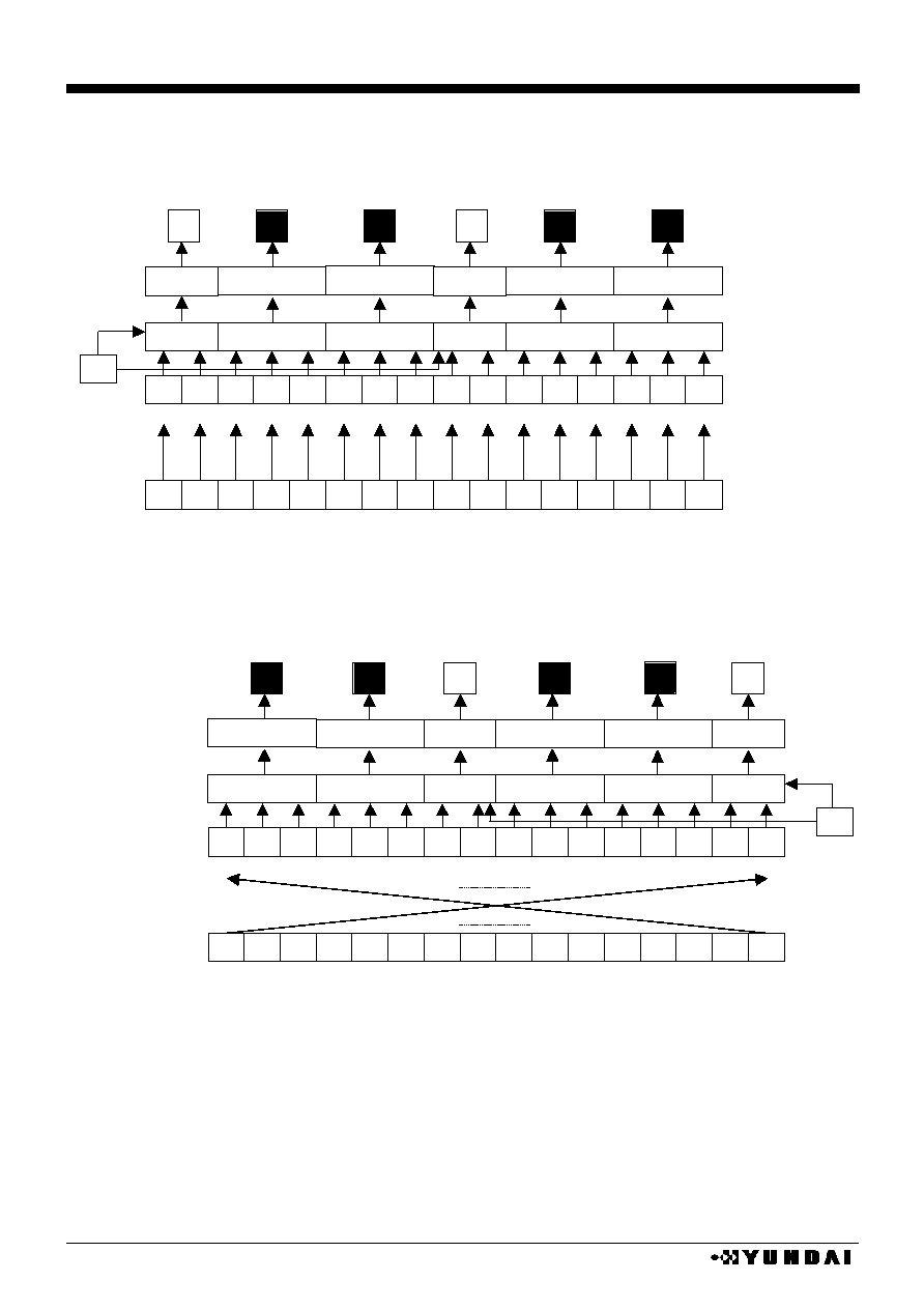
HM17CM256
- 30 -
When display RAM is accessed by 16 bit data width, the weight of each data bit is dependent on
the status of SWAP register and REF register, the same method as 8 bit access
�
ACCESS when (REF, SWAP)=(0, 0) or (1, 1)
notice) internal access X address :n
H
~3F
H
(access when REF="0")
:3F
H
~n
H
(access when REF="1")
�
ACCESS when (REF, SWAP)=(0, 1) or (1, 0)
notice) internal access X address :n
H
~3F
H
(access when REF="0")
:3F
H
~n
H
(access when REF="1")
MSB
LSB
MSB
LSB
MSB
GLSB circuit
CPU access data
X address :n
H
1
LSB
MSB
LSB
MSB
MSB
1
0
0
0 0
0
1
1 1
1
0 1
1 1
1
0
0
D
0
D
1
D
2
D
3
D
4
D
5
D
6
D
7
D
8
D
9
D
10
D
11
D
12
D
13
D
14
D
15
SEGAi
SEGBi
0
Palette Aj
SEGCi
Palette Cj
Gradation palette
i=0~126
j=0~7
Gradation
control ciruit
Display RAM data
0
0 0
0
1
1 1
1
0
0
SEGBi+1
Palette Bj
Palette Cj
Palette Bj
Palette Aj
SEGAi+1
SEGCi+1
1 1
0
0
SEGAi
SEGBi
1
Palette Aj
SEGCi
Palette Cj
MSB
LSB
MSB
LSB
MSB
GLSB circuit
Gradation palette
i=0~126
j=0~7
CPU access data
X address :n
H
Graydation
control ciruit
Display RAM data
1
0 0
1
1
1 0
0
1 1
0
LSB
MSB
LSB
MSB
MSB
SEGBi+1
Palette Bj
Palette Cj
Palette Bj
Palette Aj
SEGAi+1
SEGCi+1
1 0
0
0
0
0
0 0
0
1
1 1
1
0 1
1 1
1
0
0
0
D
0
D
1
D
2
D
3
D
4
D
5
D
6
D
7
D
8
D
9
D
10
D
11
D
12
D
13
D
14
D
15
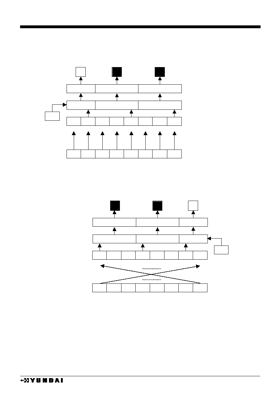
HM17CM256
- 31 -
l
DISPLAY RAM BITMAP AT BLACK & WHITE MODE (MON="1")
The MSBs of display RAM data ( 3 bit, 2 bit ) is used as display data at black and white mode.
example) 8 bit width access ( the same method as 16 bit width access)
�
ACCESS when (REF, SWAP)=(0, 0) or (1, 1)
notice) internal access X address :n
H
(access when REF="0")
:7Fn
H
~n
H
(access when REF="1")
�
ACCESS when (REF, SWAP)=(0, 1) or (1, 0)
notice) internal access X address :n
H
(access when REF="0")
:7Fn
H
~n
H
(access when REF="1")
SEGAi
SEGBi
m
n
o
p
Aj
Palette Bj
0
0
Palette Aj
1
0
0
SEGCi
Palette Cj
1
1
1
MSB LSB
MSB LSB
MSB
0
0
1
0
0
1
1
1
D
0
D
1
D
2
D
3
D
4
D
5
D
6
D
7
0
GLSB circuit
Gradation palette
i=0~127
j=0~7
CPU access data
X address :n
H
Gradation control circuit.
Display RAM data
SEGCi
SEGBi
1
1
1
0
0
SEGAi
Palette Cj
Palette Bj
Palette Aj
1
0
0
MSB
LSB MSB
LSB MSB
0
0
1
0
0
1
1
1
D
0
D
1
D
2
D
3
D
4
D
5
D
6
D
7
Gradation palette
i=0~127
j=0~7
CPU access data
X address :n
H
Gradation control circuit
Display RAM data
0
GLSB circuit

HM17CM256
- 32 -
gradation level table (MON="1", Black & white mode)
(MSB)RAM data (LSB)
Gradation level
RAM data
GLSB
Gradation level
0
0
0
0
0
0
*
0
0
0
1
0
0
1
*
0
0
1
0
0
1
0
*
1
0
1
1
0
1
1
*
1
1
0
0
1
* : Don't Care
1
0
1
1
1
1
0
1
1
1
1
1
(12) GRADATION LSB CONTROL
At 256 colors input mode, this IC provides segment driver output for 8-gradation display using
successive 3 bits of data and that for 4-gradation display using successive 2 bits of data.
The segment driver output for the 4-gradation display uses 2 bits written to the corresponding RAM
area and 1 bit supplemented by the gradation LSB circuit, and then selects 4 gradations from 8-
gradations.
At fixed gradation mode, the segment driver output for the 4-gradation display result in a gradation
level of 0 regardless of gradation LSB register, when 2 bits of data on the display RAM are "00".
When 2 bits of data on the display RAM is "11", a gradation level of 7/7 is selected regardless of
gradation LSB register. The other gradation levels are selected depending on 2 bits of data on the
display RAM and the gradation LSB register.
One bit of data is supplemented by setting the gradation LSB register (GLSB).
For this register, the bit information specified for only one time setting is used as the LSB of the
RAM for all the 4-gradation segment drivers.
Gradation LSB = "0": Set 0 as the LSB of the RAM for 4-gradation segment drivers.
Gradation LSB = "1": Set 1 as the LSB of the RAM for 4-gradation segment drivers.
(13) GRADATION PALETTE
This IC has two gradation display modes, the fixed gradation display mode and the variable
gradation display mode.
Select mode by setting the gradation display mode register (PWM command) to the purpose.
PWM="0" : variable gradation mode among 32-level gradations.
PWM="1" : fixed 8 gradation mode
To select the best gradation level suited to LCD panel at variable gradation display mode, use the
gradation palette register among 32-level gradation palettes. Segment driver outputs are set by
selected 8-level gradation palette.
The gradation palette register provides three registers ( palette Aj, Bj, and Cj : j=0
7 ) for the
segment driver outputs, SEGAi(0
127), SEGBi(0
127), and SEGCi(0
127) . Each register
consists of a 5-bit register, selecting 8 gradations from the 32 gradation pattern.
Segment driver selects 4 gradations among 8 gradation by 2 bits wrote-in RAM and 1bit calibrated
by GLSB.

HM17CM256
- 33 -
GRADATION PALETTE INITIAL VALUE
( palette Aj, palette Bj, palette Cj (j=0~7) )
(MSB)RAM data (LSB)
Register name
Initial value
0
0
0
Gradation palette 0
0 0 0 0 0
0
0
1
Gradation palette 1
0 0 1 0 1
0
1
0
Gradation palette 2
0 1 0 1 0
0
1
1
Gradation palette 3
0 1 1 1 0
1
0
0
Gradation palette 4
1 0 0 0 1
1
0
1
Gradation palette 5
1 0 1 0 1
1
1
0
Gradation palette 6
1 1 0 1 0
1
1
1
Gradation palette 7
1 1 1 1 1
GRADATION PALETTE TABLE (PWM="0", variable mode)
( palette Aj, palette Bj, palette Cj (j=0~7) )
Palette
Gradation
remark
Palette
gradation
remark
0 0 0 0 0
0
Palette 0 initial value
1 0 0 0 0
16/31
0 0 0 0 1
1/31
1 0 0 0 1
17/31
Palette 4 initial value
0 0 0 1 0
2/31
1 0 0 1 0
18/31
0 0 0 1 1
3/31
1 0 0 1 1
19/31
0 0 1 0 0
4/31
1 0 1 0 0
20/31
0 0 1 0 1
5/31
Palette 1 initial value
1 0 1 0 1
21/31
Palette 5 initial value
0 0 1 1 0
6/31
1 0 1 1 0
22/31
0 0 1 1 1
7/31
1 0 1 1 1
23/31
0 1 0 0 0
8/31
1 1 0 0 0
24/31
0 1 0 0 1
9/31
1 1 0 0 1
25/31
0 1 0 1 0
10/31
Palette 2 initial value
1 1 0 1 0
26/31
Palette 6 initial value
0 1 0 1 1
11/31
1 1 0 1 1
27/31
0 1 1 0 0
12/31
1 1 1 0 0
28/31
0 1 1 0 1
13/31
1 1 1 0 1
29/31
0 1 1 1 0
14/31
Palette 3 initial value
1 1 1 1 0
30/31
0 1 1 1 1
15/31
1 1 1 1 1
31/31
Palette 7 initial value
GRADATION PALETTE TABLE (PWM="1", fixed mode)
(MSB)RAM data(LSB)
gradation
RAM data
GLSB
gradation
0
0
0
0
0
0
0
0
0
1
1/7
0
0
1
0
0
1
0
2/7
0
1
0
2/7
0
1
1
3/7
0
1
1
3/7
1
0
0
4/7
1
0
0
4/7
1
0
1
5/7
1
0
1
5/7
1
1
0
6/7
1
1
0
1
1
1
7/7
1
1
1
7/7

HM17CM256
- 34 -
(14) DISPLAY TIMMING GENERATOR
The display-timing generator makes a timing clock and timing pulses (CL, FLM, FR and CLK) for
internal operation by inputting the original oscillating clock CK or by the oscillating circuit.
By setting up Master / Slave mode (M/S), the state of timing pulse pins and the timing generator
changes.
Display timing pulse pins and generator status
M/S port mode
CL port FR port FLM port CLK port
Timing generator status
L
Slave
Input
Input
Input
Input
CL, FLM, FR signal generator stop
H
Master Output Output Output
Output
Operating status
(15) SIGNAL GENERATION OF DISPLAY LINE COUNTER, DISPLAY DATA LATCH CIRCUIT.
The latch signal from line counter clock to display data latch circuit is generated from display clock
(CL). Synchronized with the display clock, the line addresses of Display RAM are generated and
384-bit display data are latched to display-data latching circuit and then output to the LCD drive
circuit (SEG output port).
Read-out of the display data to the LCD drive circuit is completely independent of MPU side and so
MPU can access it with no relationship with the read-out operation of the display data.
(16) GENERATION OF THE ALTERNATED SIGNAL(FR), SYNCHRONOUS SIGNAL(FLM).
The alternated signal (FR) and synchronous signal (FLM) are generated from the display clock
(CL). The FLM generates alternated drive waveform to the LCD drive circuit per frame at normal
state ( inverse FR signal level per 1 frame ). But by setting up data (n-1) on n-line inversion
register and "1" on n-line alternated command (NLIN), n-line inverse waveform can be generated.
When this HM17CM256 is used in multi-chip application, the signals of CL, FLM, FR and CLK
must be sent from master side to slave side.
(17) DISPLAY DATA LATCH CIRCUIT
This circuit latches the display data from display RAM to LCD driver circuit temporarily per every
common period. Normal / reverse display, display ON/OFF, and display all on command are done
by controlling data in this latch. And no data within display RAM changes.

HM17CM256
- 35 -
(18) EXAMPLE OF LCD DRIVING (NORMAL MODE, 1/82 DUTY, BLACK & WHITE DISPLAY MODE)
COM
1
COM
0
SE
G
1
SE
G
0
SE
G
2
COM
1
SEG
1
SEG
0
V
LCD
V
1
V
2
V
3
V
4
V
SS
V
LCD
V
1
V
2
V
3
V
4
V
SS
V
LCD
V
1
V
2
V
3
V
4
V
SS
COM
0
V
LCD
V
1
V
2
V
3
V
4
V
SS
FR
FLM
CL
82
1 2
4
3
5
82
1 2
4
3
5
82
1

HM17CM256
- 36 -
(19) LCD DRIVER CIRCUIT
This drive circuit generates four levels of LCD drive voltage. The circuit has 384 segment outputs
and 82 common outputs and outputs combined display data and FR signal.
Two of common outputs(COMI
0
,COMI
1
) are for pictograph marker display only. The common
drive circuit that has shift register and outputs common scan signals sequentially.
(20) DUMMY SEGMENT DRIVER CIRCUIT
Segment driver circuit has 6 dummy output ( SEGSA
0
~ SEGSA
3
, SEGSB
0
~ SEGSB
3
, SEGSC
0
~
SEGSC
3
) at each edge side. Normally, the segment driver output is generated by memorized
RAM data but there are no RAMs but registers for dummy segment driver. There are 8 bit registers
correspond to SEGSA
0
, SEGSB
0
, SEGSC
0
and drive LCD with same level to Y direction. ( SEGSA
1
~ SEGSA
3
, SEGSB
1
~ SEGSB
3
, SEGSC
1
~ SEGSC
3
are the same function. )
SEGSA
0
~ SEGSA
3
port is used same gradation palette with SEGA
0
~ SEGA
127
,
SEGSB
0
~
SEGSB
3
with SEGB
0
~ SEGB
127
, and SEGSC
0
~ SEGSC
3
with SEGC
0
~ SEGC
127
This circuit is effective at display of boundary or background display. The dummy segment
drivers do not depend on LREV polarity but ALLON and REV command for display
There are 4-byte registers for dummy segment driver, SEGSA
0
~ SEGSA
3
, SEGSB
0
~ SEGSB
3
,
SEGSC
0
~ SEGSC
3
, If you want to access this register, please use DMY ="1" command.
68 series
80 series
RS DMY
R/W
RD
WR
Function
0
0
1
0
1
Read out display data
0
0
0
1
0
Write in display data
0
1
1
0
1
Read out dummy segment register
0
1
0
1
0
Write in dummy segment register
There are the same rules at read out of dummy segment register as display RAM data read out
sequence. After address setting, the data of assigned address is shown directly after the end of
the read command, so pay attention that assigned data is available at 2nd timing step. In other
words, there needs 1 cycle dummy read after address set and write cycle.
1 cycle dummy read is necessary for after address setting and write cycle.
When access with DMY="1", X address is an effective value at address setting. There are 4-byte
and so 00
H
, 01
H
, 02
H
, 03
H
are effective at 8-bit mode and 00
H
, 01
H
are effective at 16-bit mode.
The access bears no relation to Y address setting.
When access with DMY="1", it is possible that the data is written into register by increment
operation.
notice) more detail information at
q
DUMMY SEGMENT REGISTER ADDRESS AND BITMAP
r
in
s
(10) Relation
between Display RAM and address
t
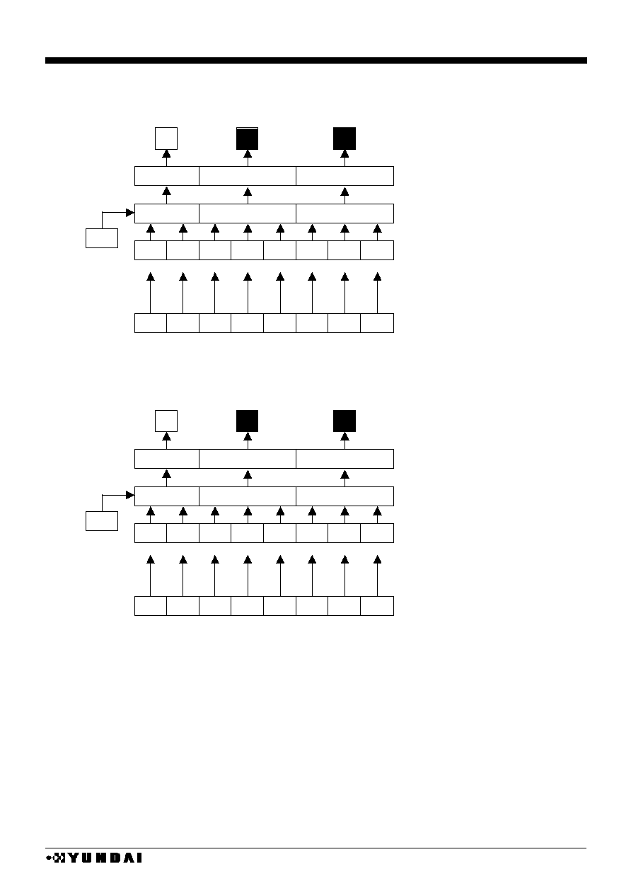
HM17CM256
- 37 -
ACCESS WITH 8 BIT BUS EXAMPLE : GRAY MODE , ACCESS UNDER (REF, SWAP)=(0, 0)
(21) OSCILLATOR CIRCUIT
HM17CM256 has the CR oscillator. The output of oscillator is used as the timing signal source of
display and boosting clock to the booster. This is valid only in the master operation mode.
When in the master operation mode and if external clock is used, feed the clock to OSC
1
pin or
connect resistor between OSC
1
and OSC
2
.
And feedback resistance with command can set the inner oscillator circuit of HM17CM256.
The frame frequency can be altered by changed oscillator frequency according to feedback
resistance length set value. To get optimum frame frequency, please check LCD and then set the
frequency of oscillator.
(22) POWER SUPPLY CIRCUIT
Gradation
palette
GLSB circuit
Gradation control circuit
Latched data
SEGSA
0
SEGSB
0
Palette Aj
Palette Bj
0
0
1
0
0
SEGSC
0
Palette Cj
1
1
1
MSB LSB
MSB LSB
MSB
0
0
1
0
0
1
1
1
D
0
D
1
D
2
D
3
D
4
D
5
D
6
D
7
0
j=0~7
CPU access data
X address :00
H
Gradation palette
Gradation control circuit
SEGSA
3
SEGSB
3
Palette Aj
Palette Bj
0
0
1
0
0
SEGSC
3
Palette Cj
1
1
1
MSB LSB
MSB LSB
MSB
0
0
1
0
0
1
1
1
D
0
D
1
D
2
D
3
D
4
D
5
D
6
D
7
0
GLSB circuit
j=0~7
CPU access data
Latched data
X address :03
H

HM17CM256
- 38 -
This block generates the voltages necessary for driving LCD panel. The power supply circuit
consists of voltage boosting circuit and voltage converting circuit and generates the voltages (V
LCD
,
V
1
, V
2
, V
3
, V
4
. ) for LCD driving.
For large panel driving, it's preferable to use external voltage source rather than to use built-in
power supply circuit for good image quality.
When using external voltage source, disable the built-in power supply circuit(AMPON, DCON=`00'),
supply the V
LCD
, V
1
, V
2
, V
3
, V
4
and V
OUT
externally and open the C
1
+, C
1
-, C
2
+, C
2
-, C
3
+, C
3
-, C
4
+, C
4
-,
C
5
+, C
5
-, C
6
+, C
6
-, V
REF
, V
REG
, V
EE
terminals.
According to power supply circuit control command input, the power supply circuit can be enabled
partially. External power supply and partial inner power circuit can be used together. Refer to the
next table.
DCON AMPON
Boosting circuit Converting circuit
External voltage input
remark
0
0
Disable
disable
V
OUT
, V
LCD
, V
1
, V
2
, V
3
, V
4
common
u
1,3
0
1
Disable
enable
V
OUT
common
u
2,3
1
1
Enable
enable
-
-
v
1. All the built-in boosting circuit, converting circuit is not used. Open the ,C
1
+, C
1
-, C
2
+, C
2
-, C
3
+, C
3
-, C
4
+,
C
4
-, C
5
+, C
5
-, C
6
+, C
6
-, V
REF
, V
REG
, V
EE
terminals, LCD driving voltage should be applied externally.
v
2.Only the Boosting circuit is not used. Open the C
1
+,C
1
-,C
2
+,C
2
-,C
3
+,C
3
-,C
4
+,C
4
-,C
5
+,C
5
-,C
6
+,C
6
-, V
OUT
terminals, The power for converting circuit must be supplied through V
OUT
terminal and the reference
voltage must be supplied by V
REF
terminal.
v
3.The conditions between V
OUT
, V
LCD
, V
1
, V
2
, V
3
, and V
4
are V
OUT
V
LCD
V
1
V
2
V
3
V
4
V
SS
.
(23) VOLTAGE BOOSTING CIRCUIT
By connecting capacitor CA
1
between C
1
+ and C
1
-, C
2
+ and C
2
-, C
3
+ and C
3
-, C
4
+ and C
4
-, C
5
+
and C
5
- , C
6
+ and C
6
-, V
OUT
and V
SS
, n-time boosted voltage of V
EE
- V
SS
can be generated through
V
OUT
port. The boosting coefficient can be set by command and 2-times/ 3-times / 4-times/ 5-
times/ 6-times/ 7-times boosted voltage is output through V
OUT
port.
At application, specific boosting coefficient is used, refer to the following description.
w
At 2-times boosting is designed, connect boosting capacitor CA
1
between C
1
+ and C
1
- , and
open C
2
+, C
2
-, C
3
+, C
3
-, C
4
+, C
4
-, C
5
+, C
5
-, C
6
+, C
6
- terminals.
x
At 3-times boosting is designed, connect boosting capacitor CA
1
between C
1
+ and C
1
- , C
2
+
and C
2
- , and open C
3
+,C
3
-, C
4
+, C
4
-, C
5
+, C
5
-, C
6
+, C
6
- terminals.
y
At 4-times boosting is designed, connect boosting capacitor CA
1
between C
1
+ and C
1
- , C
2
+
and C
2
- , C
3
+ and C
3
- , and open C
4
+, C
4
-, C
5
+, C
5
-, C
6
+, C
6
- terminals
z
At 5-times/ 6-times/ 7-times boosting are same structures with upper case.
Special care should be taken so that the voltage of VOUT would not exceed 18V MAX.
VOUT voltage exceeding 18V can cause malfunction and reliability problem.
3-times boosting
7-times boosting
V
SS
=0V
V
EE
=3V
V
OUT
=9V
V
OUT
=17.5V
V
SS
=0V
V
EE
=2.5V

HM17CM256
- 39 -
(24) ELECTRIC VOLUME
The electric volume is within voltage converting circuit and the brightness of LCD can be controlled
by adjusting V
LCD
level with command.
The LCD driving voltage V
LCD
is generated by selecting 1 level within 128 step electric volume
controlled levels by setting 7 bit electric volume register.
(25) VOLTAGE REGULATOR CIRCUIT
The voltage regulator circuit is within voltage converting circuit and generates regulated voltage
using V
REF
input with magnification by adjusting internal resistor. The generated voltage by voltage
regulator is output at V
REG
terminal. Even though boosted voltage variation, generated regulator
voltage is stable because boosting voltage level is higher than the amplified regulator voltage V
REG
.
And so, stable voltage level can be generated even if there is load variation.
V
REG
is used as input voltage of electric volume circuit to generate LCD driving voltage.
(26) REFERENCE VOLTAGE GENERATION CIRCUIT
The reference voltage generation circuit is within voltage converting circuit.
This circuit generates reference voltage V
BA
terminal for using at regulator circuit through. The
output voltage level from V
BA
terminal is as following description.
V
BA
= V
EE
x 0.9
The LCD driving voltages can be made by applying reference voltage to reference voltage input
terminal V
REF
.
(27) LCD DRIVING VOLTAGE GENERATION CIRCUIT
The generation circuit of LCD driving voltage is within voltage converting circuit and generates
voltages V
LCD
, V
1
, V
2
, V
3
, V
4
by resistively dividing V
LCD
into 4 levels.
The bias ratio of LCD driving voltages can be one of 1/5, 1/6, 1/7, 1/8, 1/9, 1/10.
When using built-in power supply circuit, you should connect voltage stabilization capacitor CA
2
at
each of LCD power terminals. There is need for selecting the coefficient of capacitor CA
2
after
display the LCD.
When using external voltage supply, disable the built-in power supply circuit(AMPON, DCON=`00'),
supply the V
OUT
, V
LCD
, V
1
, V
2
, V
3
, V
4
voltages externally and open the C
1
+ , C
1
- , C
2
+ , C
2
- , C
3
+ , C
3
- ,
C
4
+ , C
4
- , C
5
+ , C
5
- , C
6
+ , C
6
- , V
EE
, V
REF
, V
REG
terminals.
When using external voltage source and parts of built-in voltage converting circuit, the terminals of
C
1
+ , C
1
- , C
2
+ , C
2
- , C
3
+ , C
3
- , C
4
+ , C
4
- , C
5
+ , C
5
- , C
6
+ , C
6
- should be open because boosting
circuit is not activated, you should supply reference voltage through V
REF
terminal and the voltage for
voltage converting circuit at V
OUT
.
Connecting stabilization capacitor CA
3
at V
REG
terminal is recommended.
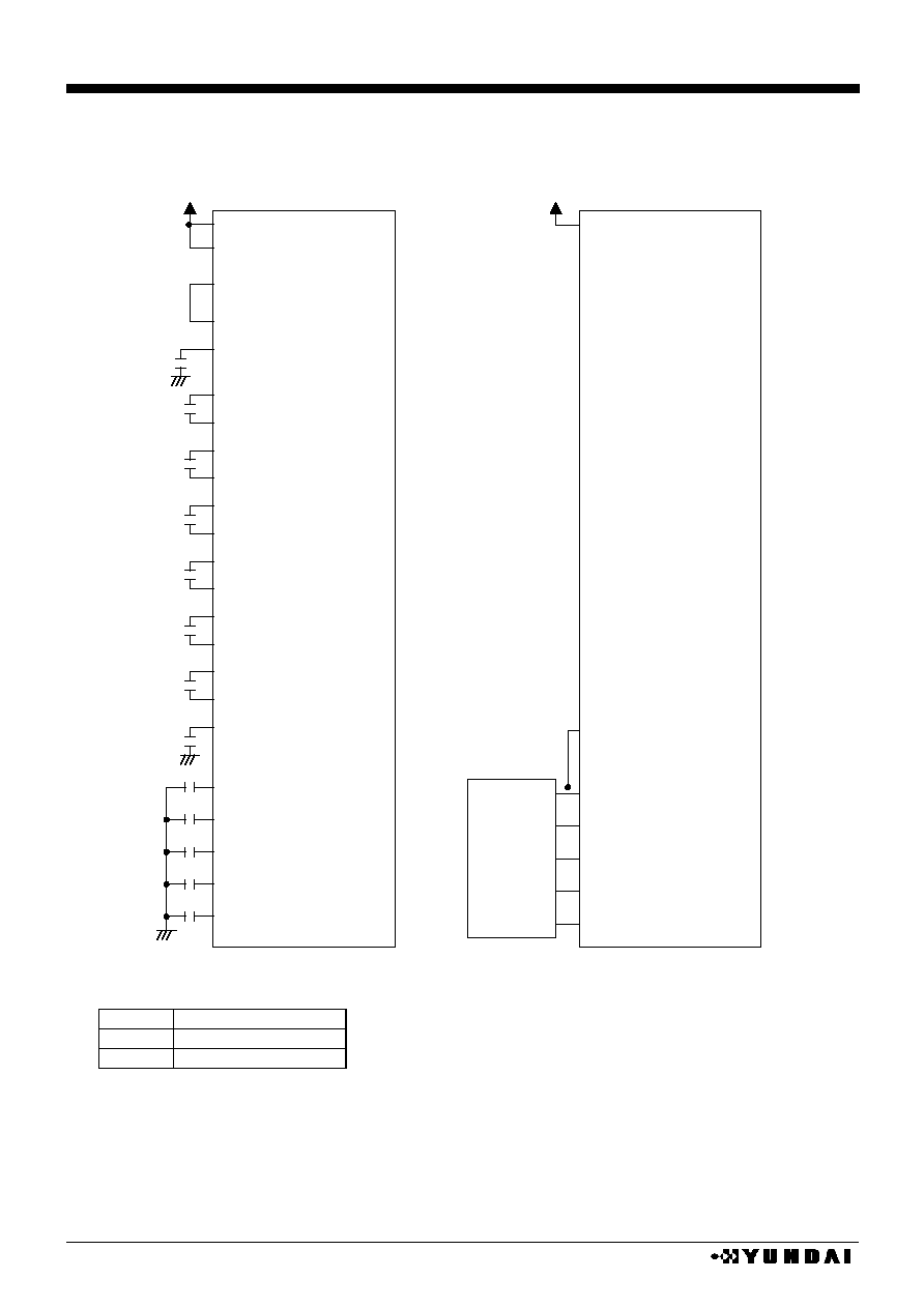
HM17CM256
- 40 -
value
CA
1
1.0 ~ 4.7
�
F
CA
2
1.0 ~ 2.2
�
F
CA
3
0.1
�
F
caution
{
Please use B grade capacitor.
internal power circuit is not used case
internal power circuit / internal reference voltage
generating circuit are activated case.(7 times boosting)
V
DD
V
EE
V
BA
V
REF
V
REG
C
1
-
C
1
+
C
2
-
C
2
+
C
3
-
C
3
+
C
4
-
C
4
+
V
OUT
V
LCD
V
1
V
2
V
3
V
4
V
DD
CA
3
V
SS
CA
1
CA
1
CA
1
CA
1
CA
1
V
SS
V
SS
CA
2
CA
2
CA
2
CA
2
CA
2
C
5
-
C
5
+
C
6
-
C
6
+
CA
1
CA
1
Extnal
power
circuit
V
DD
V
EE
V
BA
V
REF
V
REG
C
1
-
C
1
+
C
2
-
C
2
+
C
3
-
C
3
+
C
4
-
C
4
+
V
OUT
V
LCD
V
1
V
2
V
3
V
4
V
DD
V
LCD
V
1
V
2
V
3
V
4
C
5
-
C
5
+
C
6
-
C
6
+
HM17CM256
HM17CM256

HM17CM256
- 41 -
value
CA
1
1.0 ~ 4.7
�
F
CA
2
1.0 ~ 2.2
�
F
CA
3
0.1
�
F
caution
|
Please use B grade capacitor.
Internal power circuit is used case. Reference
voltage input from outside . (7 times boosting)
Internal power circuit is used case.
Temperature compensation by external
thermistor . (7 times boosting )
V
DD
V
EE
V
BA
V
REF
V
REG
C
1
-
C
1
+
C
2
-
C
2
+
C
3
-
C
3
+
C
4
-
C
4
+
V
OUT
V
LCD
V
1
V
2
V
3
V
4
V
DD
CA
3
V
SS
CA
1
CA
1
CA
1
CA
1
CA
1
V
SS
V
SS
CA
2
CA
2
CA
2
CA
2
CA
2
C
5
-
C
5
+
C
6
-
C
6
+
CA
1
CA
1
V
DD
V
EE
V
BA
V
REF
V
REG
C
1
-
C
1
+
C
2
-
C
2
+
C
3
-
C
3
+
C
4
-
C
4
+
V
OUT
V
LCD
V
1
V
2
V
3
V
4
V
DD
CA
3
V
SS
CA
1
CA
1
CA
1
CA
1
CA
1
V
SS
V
SS
CA
2
CA
2
CA
2
CA
2
CA
2
C
5
-
C
5
+
C
6
-
C
6
+
CA
1
CA
1
HM17CM256
HM17CM256
t
he
r
m
i
s
t
o
r

HM17CM256
- 42 -
value
CA
1
1.0 ~ 4.7
�
F
CA
2
1.0 ~ 2.2
�
F
CA
3
0.1
�
F
caution
}
Please use B grade capacitor.
Internal power circuit is used case. (boosting circuit is
not used, V
OUT
is supplied from outside)
HM17CM256
V
DD
V
EE
V
BA
V
REF
V
REG
C
1
-
C
1
+
C
2
-
C
2
+
C
3
-
C
3
+
C
4
-
C
4
+
V
OUT
V
LCD
V
1
V
2
V
3
V
4
V
DD
CA
3
V
SS
V
SS
CA
2
CA
2
CA
2
CA
2
CA
2
C
5
-
C
5
+
C
6
-
C
6
+
External
power
circuit

HM17CM256
- 43 -
(28) PARTIAL DISPLAY FUNCTION
HM17CM256 can realize the partial display at graphic display area on LCD panel.
Partial display is used with lower duty than normal state at driving.
And so, HM17CM256 can drive the LCD panel with lower bias ratio, lower boosting times and
lower LCD driving voltages, and that can drive the LCD panel with lower power consumption.
This function is suitable for calendar or clock display at mobile information apparatus.
PARTIAL DISPLAY IMAGE
Normal display partial display
The next sequence should be followed carefully to realize partial display function.
~
boosting coefficient
~
electric volume
~
bias ratio
~
duty ratio
~
display start line setting
~
display start command
and so on.
HYUNDAI
LCD DRIVER
Low Power and
Low Voltage
LCD DRIVER
Any display states
DISPLAY OFF(ON/OFF="0")
built-in power source OFF(DCON="0", AMPON="0")
WAIT
Setting the power supply circuit
Setting the display-related function
Built-in power source ON(DCON="1", AMPON="1")
WAIT
Display ON(ON/OFF="1")
Partial display state

HM17CM256
- 44 -
When using partial display function, the display duty can be selected among 1/17, 1/26, 1/32, 1/38,
1/47, 1/66, 1/77 by setting the LCD duty set command.
The display states such as LCD driving bias ratio, LCD Driving voltage, electric volume setting
value, boosting coefficient should be optimized to the selected LCD and display duty.
(29) DISCHARGE CIRCUIT
The discharge circuit of voltage(V
LCD
, V
1
~V
4
) stabilization capacitor is built in the HM17CM256.
To discharge the capacitors, set the DIS register to "1" or set the RES terminal to "0". When built-
in power supply circuit is used, built-in power supply circuit should be disabled before discharging of
the capacitor is executed. When external power supply(V
LCD
, V
1
~V
4
, V
OUT
) is used, external power
supply should be turned off before discharging of the capacitor is executed. Do not turn on the
internal power supply and external power supply (V
LCD
, V
1
~V
4
, V
OUT
) during discharging is executed.
(30) RESET CIRCUIT
HM17CM256 is initialized as following description when RES terminal is set to "L".
INITIAL SETTING CONDITION (default setting)
1. display RAM :unknown
2. X address :00
H
set
3. Y address :00
H
set
4. display start line :1 line value 0
H
5. display ON/OFF :display OFF
6. positive/negative :positive
7. display duty ratio :1/82
8. n line inversion :n inversion disable
9. COM shift direction :COM
0
COM
79
, COMI
0
, COMI
1
10. increment mode :increment OFF
11. REF mode :positive
12. data SWAP mode :OFF
13. electric volume :(0, 0, 0, 0, 0, 0, 0)
14. power circuit :OFF
15. display mode :gradation display mode
16. bias ratio :1/10 bias
17. gradation palette 0 :(0, 0, 0, 0, 0)
18. gradation palette 1 :(0, 0, 1, 0, 1)
19. gradation palette 2 :(0, 1, 0, 1, 0)
20. gradation palette 3 :(0, 1, 1, 1, 0)
21. gradation palette 4 :(1, 0, 0, 0, 1)
22. gradation palette 5 :(1, 0, 1, 0, 1)
23. gradation palette 6 :(1, 1, 0, 1, 0)
24. gradation palette 7 :(1, 1, 1, 1, 1)
25. gradation mode :variable mode
26. GLSB :"0"
27. RAM data length :8 bit mode
28. discharge register :"0"
Usually RES terminal is connected reset terminal of CPU, so that the chip can be initialized
simultaneously with CPU. HM17CM256 should be initialized when the power is on.

HM17CM256
- 45 -
(31) SUPPLYING POWER AND ON/OFF SEQUENCE
Special care should be taken to the next notice. Supplying the power at LCD driving voltage
terminal when the logic VDD is floating can cause over-current and damage the IC
(31-1) WHEN USING EXTERNAL POWER SUPPLY
power ON sequence
Reset the IC after supplying the logic power at V
DD
terminal, and then turn on the LCD driving
voltage at the terminals (V
LCD
, V
1
, V
2
, V
3
, V
4
).
And when internal voltage converter is used, reset the IC after supplying the logic power at
V
DD
terminal, and then supply power to V
LCD
terminal.
power OFF sequence
Execute HALT command or reset the IC to turn off the outputs of LCD driving output port, and
then turn off the LCD driving voltage after logic power OFF.
Inserting series resistor of 50 ~100
or fuse at V
LCD
or V
OUT
terminal (when only internal
voltage converting circuit is used) is recommended to prevent over-current.
This series resistor should be selected carefully because image quality can be dependent on.
(31-2) WHEN USING BUILT-IN POWER SUPPLY CIRCUIT
power ON sequence
Reset the IC after supplying the logic power at V
DD
terminal or after supplying power through
voltage common port (V
EE
) of boosting voltage generation and then operate internal power
circuit by command.
And when internal voltage converter is used, reset the IC after supplying the logic power at
V
DD
terminal, and then supply power to V
LCD
terminal.
You should turn on the display after the output level of internal power module is set.
If you do not keep this sequence, LCD can display wrong data.
power OFF sequence
To make off state of LCD driving output, cut the source to voltage common port (V
EE
) of
boosting voltage generation, the logic power at V
DD
terminal after reset the IC by HALT
command.
If V
EE
, and V
DD
are supplied from different power source, V
EE
terminal should be turned on/off
during V
DD
terminal voltage maintain voltage level specified in specification sheet.
Specially, when turn off the power, after cut the source to voltage common port (V
EE
), and then
turn off the logic power at V
DD
terminal after the voltage levels of V
EE
, V
OUT
, V
LCD
, V
1
~V
4
become
under LCD on voltage(LCD threshold voltage)level.
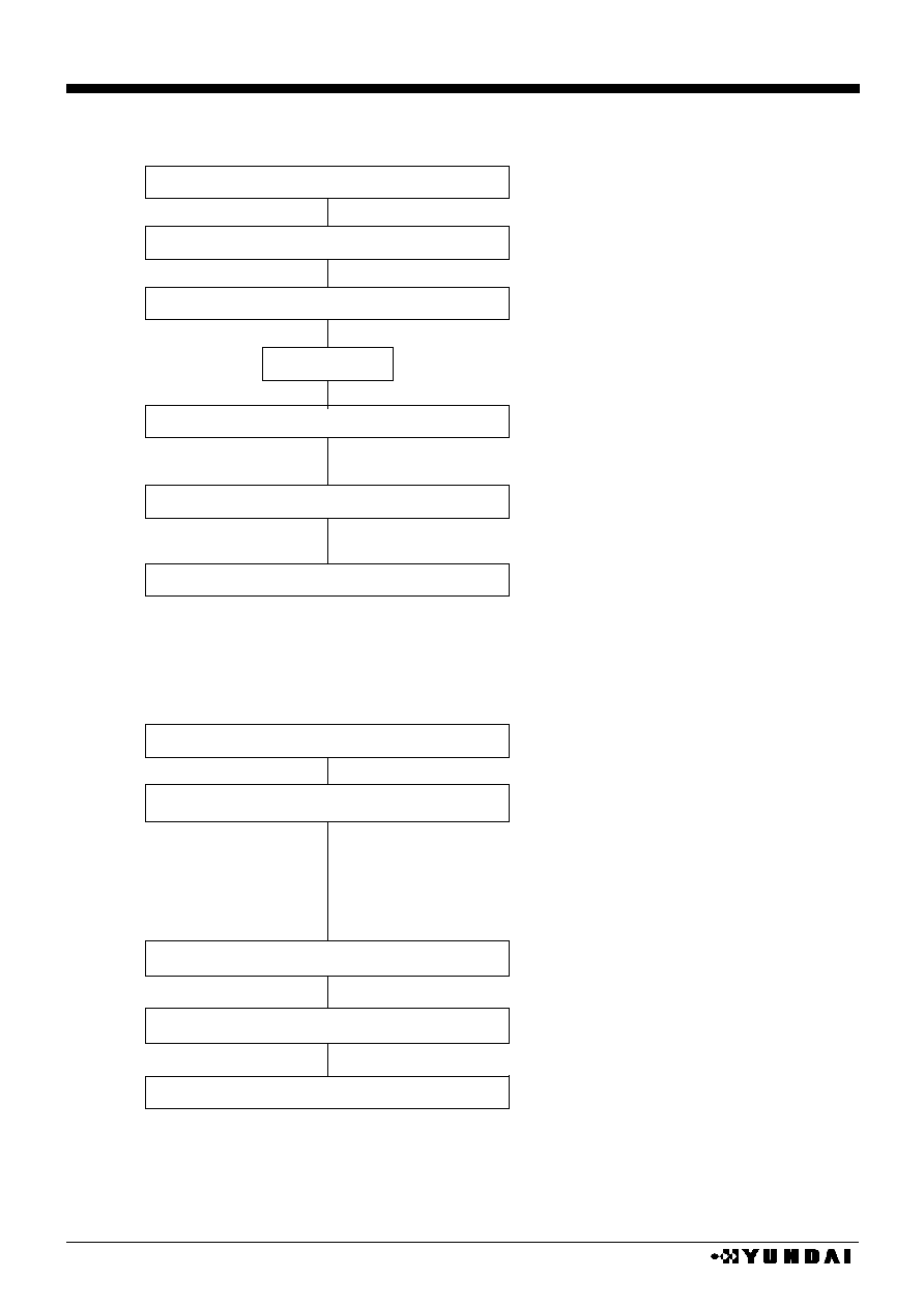
HM17CM256
- 46 -
(32) COMMAND SETTING EXAMPLE
(32-1) initial setting
electric volume code set
bias ratio set
power control set
(DCON="1", AMPON="1")
(notice) If the voltage level of VEE and VDD are different, VDD should be inputted first.
(32-2) DATA DISPLAY
display start line set
increment mode set
X address set
Y address set
display data write
display ON/OFF command set(ON/OFF="1")
V
DD
, V
EE
-V
SS
power ON
Power stable
RESET input
WAIT
Function setting by command (user setting
End of initial setting
Function setting by command (user setting
End of initialization
Function setting by command (user setting)
Data display
Function setting by command (user setting)
Function setting by command (user setting

HM17CM256
- 47 -
(32-3) POWER OFF
HALT command set or reset operation
(all LCD driver output is V
SS
level)
Discharge command set
(discharge of V
LCD
, V
1
~V
4
capacitor)
Before turning off the power, be sure to execute HALT or RESET command to make LCD
driver output OFF state.
And if V
DD
and V
EE
have different potential (V
DD
and V
EE
are not common), be sure to turn off
V
EE
first during V
DD
is supplied.
Any operation states
Function setting by command (user setting
V
EE
, V
DD
-V
SS
power OFF
WAIT

HM17CM256
- 48 -
(33) INSTRUCTION
INSTRUCTION TABLE (1)
CODE (80 series I/F)
CODE
INSTRUCTION
CS RS RD WR
RE
2
RE
1
RE
0
D
7
D
6
D
5
D
4
D
3
D
2
D
1
D
0
FUNCTION
display data write in
0 0 1 0 0/1 0/1 0/1
Write Data
Write in to display RAM
display data read out.
0 0 0 1 0/1 0/1 0/1
Read Data
Read out from display RAM
X address
(lower)
[0
H
]
0 1 1 0 0 0 0 0 0 0 0
AX
3
AX
2
AX
1
AX
0
Display RAM X direction set
X address
(upper)
[1
H
]
0 1 1 0 0 0 0 0 0 0 1 *
AX
6
AX
5
AX
4
Display RAM X direction set
Y address
(lower)
[2
H
]
0 1 1 0 0 0 0 0 0 1 0
AY
3
AY
2
AY
1
AY
0
Display RAM Y direction set
Y address
(upper)
[3
H
]
0 1 1 0 0 0 0 0 0 1 1 *
AY
6
AY
5
AY
4
Display RAM Y direction set
display start line set
(lower)
[4
H
]
0 1 1 0 0 0 0 0 1 0 0
LA
3
LA
2
LA
1
LA
0
RAM Y address setting
corresponds to scan start line of
common driver.
display start line set
(upper)
[5
H
]
0 1 1 0 0 0 0 0 1 0 1 *
LA
6
LA
5
LA
4
RAM Y address setting
corresponds to scan start line of
common driver.
N line inversion set
(lower)
[6
H
]
0 1 1 0 0 0 0 0 1 1 0 N
3
N
2
N
1
N
0
quantity setting of line inversion
N line inversion set
(upper)
[7
H
]
0 1 1 0 0 0 0 0 1 1 1 * N
6
N
5
N
4
quantity setting of line inversion
display control (1)
[8
H
]
0 1 1 0 0 0 0 1 0 0 0
SHI
FT
MO
N
ALL
ON
ON/
OFF
SHIFT: common shift direction set,
MON: BW/gradation display,
ALLON: all on ,
ON/OFF: display ON/OFF control
display control (2)
[9
H
]
0 1 1 0 0 0 0 1 0 0 1
RE
V
NL
IN
SW
AP
RE
F
REV: display positive / negative,
NLIN: n line inversion ON/OFF,
SWAP: display data swap,
REF: segment positive / negative
increment control
[A
H
]
0 1 1 0 0 0 0 1 0 1 0
WIN
AIM AYI AXI
WIN: window selection,
AIM: increment timing selection,
AYI:Y increment,
AXI:X increment
power control
[B
H
]
0 1 1 0 0 0 0 1 0 1 1
AMP
ON
HA
LT
DC
ON
AC
L
AMPON: internal OP Amp. ON,
HALT: power save
DCON: boosting circuit ON, ACL: reset
LCD duty set
[C
H
]
0 1 1 0 0 0 0 1 1 0 0 *
DS
2
DS
1
DS
0
LCD driver duty ratio set
boosting coefficient
set [D
H
]
0 1 1 0 0 0 0 1 1 0 1 *
VU
2
VU
1
VU
0
Boosting times set
bias ratio set
[E
H
]
0 1 1 0 0 0 0 1 1 1 0 * B
2
B
1
B
0
LCD drive bias set
RE register set
[F
H
]
0 1 1 0 0/1 0/1 0/1 1 1 1 1
TST
0
RE
2
RE
1
RE
0
RE flag set
Notice 1) * mark is Don't Care
Notice 2) [ ] The inner side number is an address for internal register read.
Notice 3) The commands that upper/lower register settings are demanded are effective at the point of commands input.
But electric volume is effective after upper and lower register setting.

HM17CM256
- 49 -
INSTRUCTION TABLE (2)
CODE (80 series I/F)
CODE
INSTRUCTION
CS RS RD WR
RE
2
RE
1
RE
0
D
7
D
6
D
5
D
4
D
3
D
2
D
1
D
0
FUNCTION
Gradation palette A
0
set
(lower)
[0
H
]
0 1 1 0 0 0 1 0 0 0 0
PA
03
PA
02
PA
01
PA
00
Set value to gradation palette
A
0
Gradation palette A
0
set
(upper)
[1
H
]
0 1 1 0 0 0 1 0 0 0 1 * * *
PA
04
Set value to gradation palette
A
0
Gradation palette A
1
set
(lower)
[2
H
]
0 1 1 0 0 0 1 0 0 1 0
PA
13
PA
12
PA
11
PA
10
Set value to gradation palette
A
1
Gradation palette A
1
set
(upper)
[3
H
]
0 1 1 0 0 0 1 0 0 1 1 * * *
PA
14
Set value to gradation palette
A
1
Gradation palette A
2
set
(lower)
[4
H
]
0 1 1 0 0 0 1 0 1 0 0
PA
23
PA
22
PA
21
PA
20
Set value to gradation palette
A
2
Gradation palette A
2
set
(upper)
[5
H
]
0 1 1 0 0 0 1 0 1 0 1 * * *
PA
24
Set value to gradation palette
A
2
Gradation palette A
3
set
(lower)
[6
H
]
0 1 1 0 0 0 1 0 1 1 0
PA
33
PA
32
PA
31
PA
30
Set value to gradation palette
A
3
Gradation palette A
3
set
(upper)
[7
H
]
0 1 1 0 0 0 1 0 1 1 1 * * *
PA
34
Set value to gradation palette
A
3
Gradation palette A
4
set
(lower)
[8
H
]
0 1 1 0 0 0 1 1 0 0 0
PA
43
PA
42
PA
41
PA
40
Set value to gradation palette
A
4
Gradation palette A
4
set
(upper)
[9
H
]
0 1 1 0 0 0 1 1 0 0 1 * * *
PA
44
Set value to gradation palette
A
4
Gradation palette A
5
set
(lower)
[A
H
]
0 1 1 0 0 0 1 1 0 1 0
PA
53
PA
52
PA
51
PA
50
Set value to gradation palette
A
5
Gradation palette A
5
set
(upper)
[B
H
]
0 1 1 0 0 0 1 1 0 1 1 * * *
PA
54
Set value to gradation palette
A
5
Gradation palette A
6
set
(lower)
[C
H
]
0 1 1 0 0 0 1 1 1 0 0
PA
63
PA
62
PA
61
PA
60
Set value to gradation palette
A
6
Gradation palette A
6
set
(upper)
[D
H
]
0 1 1 0 0 0 1 1 1 0 1 * * *
PA
64
Set value to gradation palette
A
6
RE register set
[F
H
]
0 1 1 0 0/1 0/1 0/1 1 1 1 1
TST
0
RE
2
RE
1
RE
0
RE flag set
Notice 1) * mark is Don't Care
Notice 2) [ ] The inner side number is an address for internal register read.
Notice 3) The commands that upper/lower register settings are demanded are effective at the point of commands input.
But electric volume is effective after upper and lower register setting.
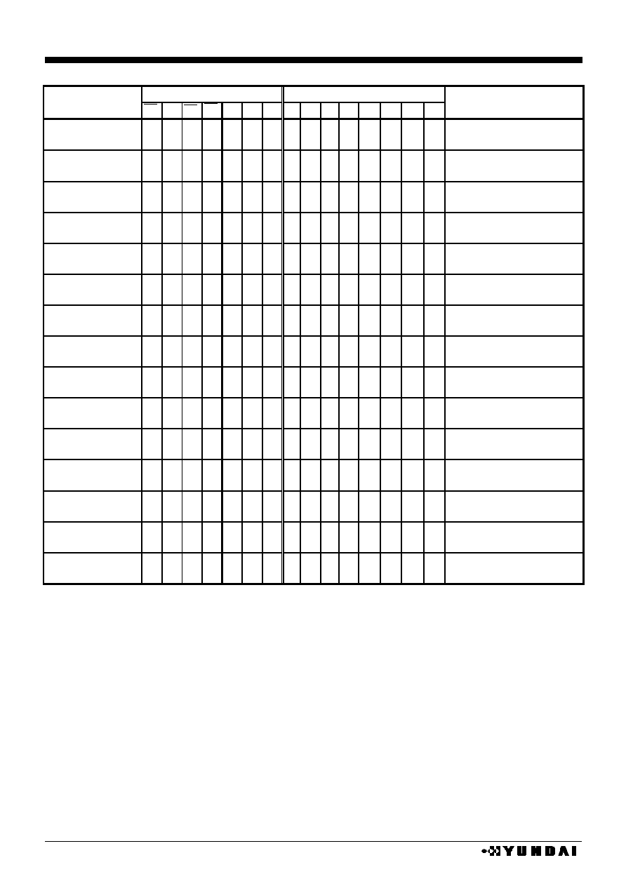
HM17CM256
- 50 -
INSTRUCTION TABLE (3)
CODE (80 series I/F)
CODE
INSTRUCTION
CS RS RD WR
RE
2
RE
1
RE
0
D
7
D
6
D
5
D
4
D
3
D
2
D
1
D
0
FUNCTION
Gradation palette A
7
set
(lower)
[0
H
]
0 1 1 0 0 1 0 0 0 0 0
PA
73
PA
72
PA
71
PA
70
Set value to gradation palette
A
7
Gradation palette A
7
set
(upper)
[1
H
]
0 1 1 0 0 1 0 0 0 0 1 * * *
PA
74
Set value to gradation palette
A
7
Gradation palette B
0
set
(lower)
[2
H
]
0 1 1 0 0 1 0 0 0 1 0
PB
03
PB
02
PB
01
PB
00
Set value to gradation palette
B
0
Gradation palette B
0
set
(upper)
[3
H
]
0 1 1 0 0 1 0 0 0 1 1 * * *
PB
04
Set value to gradation palette
B
0
Gradation palette B
1
set
(lower)
[4
H
]
0 1 1 0 0 1 0 0 1 0 0
PB
13
PB
12
PB
11
PB
10
Set value to gradation palette
B
1
Gradation palette B
1
set
(upper)
[5
H
]
0 1 1 0 0 1 0 0 1 0 1 * * *
PB
14
Set value to gradation palette
B
1
Gradation palette B
2
set
(lower)
[6
H
]
0 1 1 0 0 1 0 0 1 1 0
PB
23
PB
22
PB
21
PB
20
Set value to gradation palette
B
2
Gradation palette B
2
set
(upper)
[7
H
]
0 1 1 0 0 1 0 0 1 1 1 * * *
PB
24
Set value to gradation palette
B
2
Gradation palette B
3
set
(lower)
[8
H
]
0 1 1 0 0 1 0 1 0 0 0
PB
33
PB
32
PB
31
PB
30
Set value to gradation palette
B
3
Gradation palette B
3
set
(upper)
[9
H
]
0 1 1 0 0 1 0 1 0 0 1 * * *
PB
34
Set value to gradation palette
B
3
Gradation palette B
4
set
(lower)
[A
H
]
0 1 1 0 0 1 0 1 0 1 0
PB
43
PB
42
PB
41
PB
40
Set value to gradation palette
B
4
Gradation palette B
4
set
(upper)
[B
H
]
0 1 1 0 0 1 0 1 0 1 1 * * *
PB
44
Set value to gradation palette
B
4
Gradation palette B
5
set
(lower)
[C
H
]
0 1 1 0 0 1 0 1 1 0 0
PB
53
PB
52
PB
51
PB
50
Set value to gradation palette
B
5
Gradation palette B
5
set
(upper)
[D
H
]
0 1 1 0 0 1 0 1 1 0 1 * * *
PB
54
Set value to gradation palette
B
5
RE register set
[F
H
]
0 1 1 0 0/1 0/1 0/1 1 1 1 1
TST
0
RE
2
RE
1
RE
0
RE flag set
Notice 1) * mark is Don't Care
Notice 2) [ ] The inner side number is an address for internal register read.
Notice 3) The commands that upper/lower register settings are demanded are effective at the point of commands input.
But electric volume is effective after upper and lower register setting.
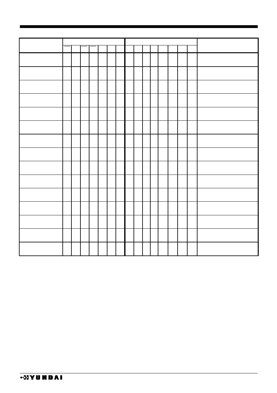
HM17CM256
- 51 -
INSTRUCTION TABLE (4)
CODE (80 series I/F)
CODE
INSTRUCTION
CS RS RD WR
RE
2
RE
1
RE
0
D
7
D
6
D
5
D
4
D
3
D
2
D
1
D
0
FUNCTION
Gradation palette B
6
set
(lower)
[0
H
]
0 1 1 0 0 1 1 0 0 0 0
PB
63
PB
62
PB
61
PB
60
Set value to gradation palette
B
6
Gradation palette B
6
set
(upper)
[1
H
]
0 1 1 0 0 1 1 0 0 0 1 * * *
PB
64
Set value to gradation palette
B
6
Gradation palette B
7
set
(lower)
[2
H
]
0 1 1 0 0 1 1 0 0 1 0
PB
73
PB
72
PB
71
PB
70
Set value to gradation palette
B
7
Gradation palette B
7
set
(upper)
[3
H
]
0 1 1 0 0 1 1 0 0 1 1 * * *
PB
74
Set value to gradation palette
B
7
Gradation palette C
0
set
(lower)
[4
H
]
0 1 1 0 0 1 1 0 1 0 0
PC
03
PC
02
PC
01
PC
00
Set value to gradation palette
C
0
Gradation palette C
0
set
(upper)
[5
H
]
0 1 1 0 0 1 1 0 1 0 1 * * *
PC
04
Set value to gradation palette
C
0
Gradation palette C
1
set
(lower)
[6
H
]
0 1 1 0 0 1 1 0 1 1 0
PC
13
PC
12
PC
11
PC
10
Set value to gradation palette
C
1
Gradation palette C
1
set
(upper)
[7
H
]
0 1 1 0 0 1 1 0 1 1 1 * * *
PC
14
Set value to gradation palette
C
1
Gradation palette C
2
set
(lower)
[8
H
]
0 1 1 0 0 1 1 1 0 0 0
PC
23
PC
22
PC
21
PC
20
Set value to gradation palette
C
2
Gradation palette C
2
set
(upper)
[9
H
]
0 1 1 0 0 1 1 1 0 0 1 * * *
PC
24
Set value to gradation palette
C
2
Gradation palette C
3
set
(lower)
[A
H
]
0 1 1 0 0 1 1 1 0 1 0
PC
33
PC
32
PC
31
PC
30
Set value to gradation palette
C
3
Gradation palette C
3
set
(upper)
[B
H
]
0 1 1 0 0 1 1 1 0 1 1 * * *
PC
34
Set value to gradation palette
C
3
Gradation palette C
4
set
(lower)
[C
H
]
0 1 1 0 0 1 1 1 1 0 0
PC
43
PC
42
PC
41
PC
40
Set value to gradation palette
C
4
Gradation palette C
4
set
(upper)
[D
H
]
0 1 1 0 0 1 1 1 1 0 1 * * *
PC
44
Set value to gradation palette
C
4
RE register set
[F
H
]
0 1 1 0 0/1 0/1 0/1 1 1 1 1
TST
0
RE
2
RE
1
RE
0
RE flag set
Notice 1) * mark is Don't Care
Notice 2) [ ] The inner side number is an address for internal register read.
Notice 3) The commands that upper/lower register settings are demanded are effective at the point of commands input.
But electric volume is effective after upper and lower register setting.

HM17CM256
- 52 -
INSTRUCTION TABLE (5)
CODE (80 series I/F)
CODE
INSTRUCTION
CS RS RD WR
RE
2
RE
1
RE
0
D
7
D
6
D
5
D
4
D
3
D
2
D
1
D
0
FUNCTION
Gradation palette C
5
set
(lower)
[0
H
]
0 1 1 0 1 0 0 0 0 0 0
PC
53
PC
52
PC
51
PC
50
Set value to gradation palette
C
5
Gradation palette C
5
set
(upper)
[1
H
]
0 1 1 0 1 0 0 0 0 0 1 * * *
PC
54
Set value to gradation palette
C
5
Gradation palette C
6
set
(lower)
[2
H
]
0 1 1 0 1 0 0 0 0 1 0
PC
63
PC
62
PC
61
PC
60
Set value to gradation palette
C
6
Gradation palette C
6
set
(upper)
[3
H
]
0 1 1 0 1 0 0 0 0 1 1 * * *
PC
64
Set value to gradation palette
C
6
Gradation palette C
7
set
(lower)
[4
H
]
0 1 1 0 1 0 0 0 1 0 0
PC
73
PC
72
PC
71
PC
70
Set value to gradation palette
C
7
Gradation palette C
7
set
(upper)
[5
H
]
0 1 1 0 1 0 0 0 1 0 1 * * *
PC
74
Set value to gradation palette
C
7
Display start command
set
[6
H
]
0 1 1 0 1 0 0 0 1 1 0 *
SC
2
SC
1
SC
0
Common drive scan start line
set
Serial extension CS
control
[7
H
]
0 1 1 0 1 0 0 0 1 1 1 * * *
EX
CS
Serial I/F, extension CS port
(EXCS) control
Display selection
control
[8
H
]
0 1 1 0 1 0 0 1 0 0 0
PW
M
GL
SB
* *
Gradation display set
RAM data length set
[9
H
]
0 1 1 0 1 0 0 1 0 0 1 * *
CKS
WL
S
RAM access data length set
8 bit/16 bit selection
Electric volume
control
(lower)
[A
H
]
0 1 1 0 1 0 0 1 0 1 0
DV
3
DV
2
DV
1
DV
0
Electric volume level set
(lower bit)
Electric volume
control
(upper) [B
H
]
0 1 1 0 1 0 0 1 0 1 1 *
DV
6
DV
5
DV
4
Electric volume level set
(upper bit)
Oscillator Rf control
[D
H
]
0 1 1 0 1 0 0 1 1 0 1
FFL
RF
2
RF
1
RF
0
RF: oscillator feed back resistor set
FFL: oscillator frequency control
discharge
[E
H
]
0 1 1 0 1 0 0 1 1 1 0 * * *
DIS
V
LCD
, V
1
~V
4
capacitor
discharge
RE register set
[F
H
]
0 1 1 0 0/1 0/1 0/1 1 1 1 1
TST
0
RE
2
RE
1
RE
0
RE flag set
Internal register read
address set
[C
H
]
0 1 1 0 1 0 0 1 1 0 0
Register read
address
Internal register read out
address set
Internal register read
0 1 0 1 0/1 0/1 0/1 * * * *
Read Data
Internal register read out
Notice 1) * mark is Don't Care
Notice 2) [ ] The inner side number is an address for internal register read.
Notice 3) The commands that upper/lower register settings are demanded are effective at the point of commands input.
But electric volume is effective after upper and lower register setting.
Notice 4) CKS=0: internal oscillation mode
CKS=1: external oscillation mode
Default CSK=0

HM17CM256
- 53 -
INSTRUCTION TABLE (6)
CODE (80 series I/F)
CODE
INSTRUCTION
CS RS RD WR
RE
2
RE
1
RE
0
D
7
D
6
D
5
D
4
D
3
D
2
D
1
D
0
FUNCTION
Window end
X
address
(lower)
[0
H
]
0 1 1 0 1 0 1 0 0 0 0
EX
3
EX
2
EX
1
EX
0
Window mode X direction end
address set
Window end
X
address
(upper
) [1
H
]
0 1 1 0 1 0 1 0 0 0 1 *
EX
6
EX
5
EX
4
Window mode X direction end
address set
Window end
Y
address
(lower
) [2
H
]
0 1 1 0 1 0 1 0 0 1 0
EY
3
EY
2
EY
1
EY
0
Window mode Y direction end
address set
Window end
Y
address
(upper)
[3
H
]
0 1 1 0 1 0 1 0 0 1 1 *
EY
6
EY
5
EY
4
Window mode Y direction end
address set
Line inversion start
Address (lower)
[4
H
]
0 1 1 0 1 0 1 0 1 0 0
LS
3
LS
2
LS
1
LS
0
Line inversion start address set
Line inversion start
address (upper)
[5
H
]
0 1 1 0 1 0 1 0 1 0 1 *
LS
6
LS
5
LS
4
Line inversion start address set
Line inversion end
Address (lower)
[6
H
]
0 1 1 0 1 0 1 0 1 1 0
LE
3
LE
2
LE
1
LE
0
Line inversion end address set
Line inversion end
Address (upper)
[7
H
]
0 1 1 0 1 0 1 0 1 1 1 *
LE
6
LE
5
LE
4
Line inversion end address set
Line inversion
control [8
H
]
0 1 1 0 1 0 1 1 0 0 0 * *
BT
LR
EV
LREV,BT: line inversion display set
Dummy segment
driver address set
[9
H
]
0 1 1 0 1 0 1 1 0 0 1 * * *
DM
Y
Dummy segment driver
address selection
PWM mode control
[A
H
]
0 1 1 0 1 0 1 1 0 1 0
PW
MS
PW
MA
PW
MB
PW
MC
PWM mode selection
RE register set
[F
H
]
0 1 1 0 0/1 0/1 0/1 1 1 1 1
TST
0
RE
2
RE
1
RE
0
RE flag set
Notice 1) * mark is Don't Care
Notice 2) [ ] The inner side number is an address for internal register read.
Notice 3) The commands that upper/lower register settings are demanded are effective at the point of commands input.
But electric volume is effective after upper and lower register setting.

HM17CM256
- 54 -
(34) INSTRUCTION DESCRIPTION
As shown in instruction table, HM17CM256 has abundant command set
.
All the data code and command code are valid only when the chip select signal CS is at "0" state.
The left side of the following command code and data table are the setting of 80 series CPU`
interface. Do not use undefined command code.
(34-1) Write display data on RAM
CS RS RD WR RE
2
RE
1
RE
0
D
7
D
6
D
5
D
4
D
3
D
2
D
1
D
0
0
0
1
0
0/1 0/1 0/1
Display RAM write data
Writing the 8-bit display RAM data at specified X, Y address.
(34-2) Read display data from RAM
CS RS RD WR RE
2
RE
1
RE
0
D
7
D
6
D
5
D
4
D
3
D
2
D
1
D
0
0
0
0
1
0/1 0/1 0/1
Display RAM read data
Reading out the 8-bit display RAM data from specified X, Y address.
One Dummy read cycle is needed after X, Y address is set.
(34-3) X address register set
CS RS RD WR RE
2
RE
1
RE
0
D
7
D
6
D
5
D
4
D
3
D
2
D
1
D
0
0
1
1
0
0
0
0
0
0
0
0
AX
3
AX
2
AX
1
AX
0
( reset :AX
3
~AX
4
=0
H
, read address :0
H
)
CS RS RD WR RE
2
RE
1
RE
0
D
7
D
6
D
5
D
4
D
3
D
2
D
1
D
0
0
1
1
0
0
0
0
0
0
0
1
*
AX
6
AX
5
AX
4
( reset :AX
6
~AX
4
=0
H
, read address :1
H
)
* : "Don't care"
Setting the X direction address address set. The lower 4-bits are set first, and then upper 3-bits are set later.
Please set from lower bit.
(34-4) Y address register set
CS RS RD WR RE
2
RE
1
RE
0
D
7
D
6
D
5
D
4
D
3
D
2
D
1
D
0
0
1
1
0
0
0
0
0
0
1
0
AY
3
AY
2
AY
1
AY
0
( reset :AY
3
~AY
0
=0
H
, read address :2
H
)
CS RS RD WR RE
2
RE
1
RE
0
D
7
D
6
D
5
D
4
D
3
D
2
D
1
D
0
0
1
1
0
0
0
0
0
0
1
1
*
AY
6
AY
5
AY
4
( reset :AY
6
~AY
4
=0
H
, read address :3
H
)
* : "Don't care"
Setting the Y address of display RAM. The lower 4-bits are set first, and then upper 3-bits are set later.
Please set from lower bit.
00
H
~51
H
is valid range at Y address(AY
6
~AY
0
). Do not use 52
H
~FF
H
range. The Y address(AY
6
~AY
0
) of
50
H
,51
H
is used for ICON display data address.

HM17CM256
- 55 -
(34-5) Display start line register set
CS RS RD WR RE
2
RE
1
RE
0
D
7
D
6
D
5
D
4
D
3
D
2
D
1
D
0
0
1
1
0
0
0
0
0
1
0
0
LA
3
LA
2
LA
1
LA
0
(reset:LA
3
~LA
0
=0
H
, read address:4
H
)
CS RS RD WR RE
2
RE
1
RE
0
D
7
D
6
D
5
D
4
D
3
D
2
D
1
D
0
0
1
1
0
0
0
0
0
1
0
1
*
LA
6
LA
5
LA
4
(reset:LA
6
~LA
4
=0
H
, read address:5
H
)
* : "Don't care"
Setting the line address of COM
0
. The address stored at the start line register becomes display line at
COM
0
line of LCD panel.
The display of LCD panel is done from line address value to the direction of increase.
LA
6
LA
5
LA
4
LA
3
LA
2
LA
1
LA
0
Line address
0
0
0
0
0
0
0
0
0
0
0
0
0
0
1
1
:
:
:
:
1
0
0
1
1
1
1
79
(34-6) n line inversion register set
CS RS RD WR RE
2
RE
1
RE
0
D
7
D
6
D
5
D
4
D
3
D
2
D
1
D
0
0
1
1
0
0
0
0
0
1
1
0
N
3
N
2
N
1
N
0
( reset :N
3
~N
0
=0
H
, read address :6
H
)
CS RS RD WR RE
2
RE
1
RE
0
D
7
D
6
D
5
D
4
D
3
D
2
D
1
D
0
0
1
1
0
0
0
0
0
1
1
1
*
N
6
N
5
N
4
( reset :N
6
~N
4
=0
H
, read address :7
H
)
* : "Don't care"
Setting line number to be inversed to register. Setting range is from 2 to 80. N line inversion register
can be effective only when N line inversion command NLIN=`1
".
If NLIN="0", the polarity of LCD driving voltage is inverted by every other frame.
N
6
N
5
N
4
N
3
N
2
N
1
N
0
Inversion line number
0
0
0
0
0
0
0
Forbidden *
0
0
0
0
0
0
1
2
:
:
:
:
1
0
0
1
1
1
1
80
n=N-1
* : N
0
~N
6
="0" is forbidden.

HM17CM256
- 56 -
�
Inversion timing
a) when n-line inversion function is OFF(1/82 duty display)
b) when n-line inversion function is ON
(34-7) display control (1) register set
CS RS RD WR RE
2
RE
1
RE
0
D
7
D
6
D
5
D
4
D
3
D
2
D
1
D
0
0
1
1
0
0
0
0
1
0
0
0
SHIFT MON
ALLON
ON/OFF
( reset :{SHIFT, MON, ALLON, ON/OFF}=0
H
, read address : 8
H
)
various control setting of display
a) ON/OFF command
Display ON/OFF control
ON/OFF="0": display OFF (all ports are V
SS
level)
ON/OFF="1": display ON
b) ALLON command
Setting display data to "1" with independence of RAM data. This command has higher priority than
positive display/negative display command. RAM data is not changed.
ALLON="0": normal display state
ALLON="1": turn on all the pixel
c) MON command
BW display / gradation display selection
MON="0": gradation display mode
MON="1": BW display mode
d) SHIFT command
Selection of the shift direction of scan data of common driver output
SHIFT="0":COM
0
COM
79
shift
SHIFT="1":COM
79
COM
0
shift
LP
FLM
FR
LP
FR
2 line
82 line
N line control
1 line
3 line
1 line
81 line
2 line
1 line
3 line
1 line
N line
2 line

HM17CM256
- 57 -
(34-8) Display control (2) register set
CS RS RD WR RE
2
RE
1
RE
0
D
7
D
6
D
5
D
4
D
3
D
2
D
1
D
0
0
1
1
0
0
0
0
1
0
0
1
REV
NLIN
SWAP
REF
( reset :{REV, NLIN, SWAP, REF}=0
H
, read address :9
H
)
various control setting of display
a) REF command
When CPU tries to access display RAM, the relation between X address and write data is changed by
command, normal or headfirst.
The output sequence of display data to segment driver can be controlled by register setting. The IC can
be placed in panel with less constraint at application.
b) SWAP command
When CPU tries to access display RAM, the display data can be swapped.
SWAP="0": Normal state, D
7
~D
0
or D
15
~D
0
are written to the RAM.
SWAP="1": SWAP mode on : The swapped data of D
7
~D
0
or D
15
~D
0
are written to the RAM.
SWAP="0"
SWAP="1"
Write data
D
7
D
6
D
5
D
4
D
3
D
2
D
1
D
0
D
7
D
6
D
5
D
4
D
3
D
2
D
1
D
0
Internal data
d
7
d
6
d
5
d
4
d
3
d
2
d
1
d
0
d
0
d
1
d
2
d
3
d
4
d
5
d
6
d
7
Read data
D
7
D
6
D
5
D
4
D
3
D
2
D
1
D
0
D
7
D
6
D
5
D
4
D
3
D
2
D
1
D
0
c) NLIN command
n line inversion ON/OFF control.
NLIN="0": n line inversion OFF. Polarity signal, FR is inverted every other frame.
NLIN="1": n line inversion ON. The n lines are inverted according to the contents of n line inversion
register
d) REV command
The relation between RAM data and display data is defined by this command.
REV="0": The display data are reflected the RAM data until that time.
REV="1": The display data are reflected the opposite data from RAM data.

HM17CM256
- 58 -
(34-9) Increment control register set
CS RS RD WR RE
2
RE
1
RE
0
D
7
D
6
D
5
D
4
D
3
D
2
D
1
D
0
0
1
1
0
0
0
0
1
0
1
0 WIN AIM AYI AXI
(reset :{WIN, AIM, AYI, AXI}=0
H
, read address :A
H
)
* : "Don't care"
Sets the display RAM address to increment mode when RAM data is accessed.
Per RAM write or read access, the increment or non-increment settings of X and Y address counter are
possible by AIM, AYI, AXI register setting. When accessing consecutive RAM areas by read or write,
the address increment operation is possible without setting the read or write address by this register setting.
After setting the auto increment register, the X, Y address should be set lower bits first.
Please revise X, Y address register after increment register setting.
When WIN register is set to "1", the CPU accesses specified area of display RAM. In this case X, Y
address should be used with auto increment mode set (AXI="1", AYI="1"). Do not revise X, Y address
register when it is not auto increment mode.
WIN="0": normal display RAM access
WIN="1": window area access at display RAM
The window to be accessed is defined by setting the start X, Y address and end X, Y address.
When accessing display with window area mode, please set X, Y start address and then X, Y window
end address.
When accessing consecutive RAM area, it is possible to access next location without setting the address
by using this command. X, Y address is unknown after auto increment setting. When WIN register is set
to "1", the RAM should be accessed after setting start point address and end point address.
And address setting should be done in sequence of start point of X address and Y address, and then
end point of X address and Y address after WIN command setting ( WIN="1").
The relationship between AIM, AYI, AXI register and X, Y address increment mode is as follow.
AIM
Increment timing selection
Remark
0
Both case of writing in and read out display RAM
1
Only when writing in display RAM( read modify)
notice
This mode is valid when read or write is performed on consecutive RAM location.
notice
This mode is valid when read out consecutive data and modifying the data and then write them in again or
read
write per access.
AYI
AXI
Increment timing selection
Remark
0
0
No increment
0
1
X address auto increment
1
0
Y address auto increment
1
1
X, Y address auto increment
notice
Regardless of AIM setting, no auto increment for X and Y address
notice
According to AIM setting, auto increment only for X address.
And X address is increased as followed loop according to REF register( SEG output direction setting
register ) value.
) Please refer to
RAM address bitmap
in
(10) relation between display RAM and address
notice
According to AIM setting, auto increment only for Y address
Y address is increased as followed loop regardless of REF register.
00
H
Max
H

HM17CM256
- 59 -
notice
According to AIM setting, auto increment for X and Y address
X address is increased to Max
H
first and then Y address is increased later.
You should set X address, Y address in sequence, anything else is forbidden.
)
Please refer to
RAM address bitmap
in
(10) relation between display RAM and address
And when X, Y auto increment mode operating, window access is possible. When window mode is
selected ( WIN ="1" ), address is increased as following loop.
a) 8 bit access mode
The increment operating is as above description.
b) 16 bit access mode
Two-byte access is done by single RAM access.
Address is increased after access.
X address is increased as (00
H
, 01
H
,
3E
H
, 3F
H
) sequence.
51
H
00
H
Max
H
00
H
51
H
00
H
X address
Y address
START
Address
X address
Y address
END
Address
START
Address
END
Address

HM17CM256
- 60 -
(34-10) Power control register set
CS RS RD WR RE
2
RE
1
RE
0
D
7
D
6
D
5
D
4
D
3
D
2
D
1
D
0
0
1
1
0
0
0
0
1
0
1
1
AMPON HALT DCON ACL
( reset :{AMPON, HALT, DCON, ACL}=0
H
�
read address :B
H
)
a) ACL command
This command initializes internal circuit and it is valid only at master operating.
ACL="0": normal state
ACL="1": initialization ON
Just after the execution of ACL command (ACL="1"), D
0
bit is set to 1. But as the initialization process
goes on internally, D
0
is reset to "0".
When ACL command is executed, internal reset signal is produced by using local display clock ( clock
from internal oscillator or from external resistor oscillation mode ).
So, after ACL command is executed, it needs to WAIT at least 2 period of the clock for next process
beginning.
ACL command is effective only at master mode operation because it uses original oscillator clock.
It is prohibited for slave mode operation to use the internal oscillator or external oscillator.
So, ACL command is impossible at slave mode. Please reset the slave device at RES terminal, when
needed.
b) DCON command
ON/OFF the internal voltage boosting circuit.
DCON="0": boosting circuit OFF
DCON="1": boosting circuit ON
c) HALT command
Power save mode ON/OFF control
HALT="0": normal state
HALT="1": power save state
The power consumption is decreased near static current at power save mode.
States of each sub-block in power save mode are as follow.
�
Oscillator, built-in power supply block stop.
�
Stop driving LCD panel, segment drive, the outputs of common driver are all set to V
SS
level.
�
Clock input from OSC
1
port is disabled.
�
Display RAM data are conserved.
�
Operational modes are preserved as those before power save command was executed.
�
V
LCD
, V
1
~ V
4
become high impedance state.
Make display OFF state before power save mode by HALT command.
And when returning from power save mode, you should display ON after oscillator, power circuit is
activated stably.
After display OFF and HALT command, if the display is turned ON before oscillator and power circuit is
not activated stably, wrong display can be appeared.
d) AMPON command
ON/OFF the internal OP. amplifier circuit of power block (voltage regulator block, electric volume,
voltage converting circuit ).
AMPON="0": internal power circuit OP. Amplifier OFF
AMPON="1": internal power circuit OP. Amplifier ON
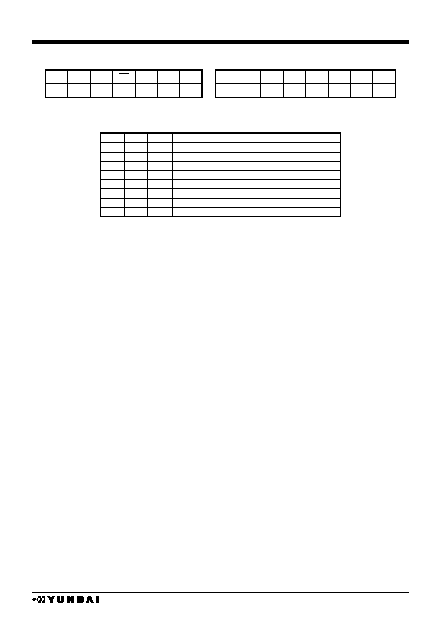
HM17CM256
- 61 -
(34-11) LCD duty set
CS RS RD WR RE
2
RE
1
RE
0
D
7
D
6
D
5
D
4
D
3
D
2
D
1
D
0
0
1
1
0
0
0
0
1
1
0
0
*
DS
2
DS
1
DS
0
( reset :{DS
2
, DS
1
, DS
0
}=0
H
�
read address :C
H
)
*:"Don't care"
LCD display duty setting
DS
2
DS
1
DS
0
duty
0
0
0
Y direction 80 dot width display, 1/82 duty
0
0
1
Y direction 75 dot width display, 1/77 duty
0
1
0
Y direction 64 dot width display, 1/66 duty
0
1
1
Y direction 45 dot width display, 1/47 duty
1
0
0
Y direction 30 dot width display, 1/32 duty
1
0
1
Y direction 15 dot width display, 1/17 duty
1
1
0
Y direction 36 dot width display, 1/38 duty
1
1
1
Y direction 24 dot width display, 1/26 duty
Partial display is possible by setting duty operation.

HM17CM256
- 62 -
(34-12) Boosting coefficient setting
CS RS RD WR RE
2
RE
1
RE
0
D
7
D
6
D
5
D
4
D
3
D
2
D
1
D
0
0
1
1
0
0
0
0
1
1
0
1
*
VU
2
VU
1
VU
0
( reset :{VU
2
~VU
0
}=0
H
�
read address :D
H
)
* : "Don't care"
coefficient setting of boosting circuit
VU
2
VU
1
VU
0
Boosting multiple
0
0
0
No boosting *
0
0
1
2 times boosting operation
0
1
0
3 times boosting operation
0
1
1
4 times boosting operation
1
0
0
5 times boosting operation
1
0
1
6 times boosting operation
1
1
0
7 times boosting operation
1
1
1
forbidden
*V
REG
amplifier gain is 1.
(34-13) Bias setting register
CS RS RD WR RE
2
RE
1
RE
0
D
7
D
6
D
5
D
4
D
3
D
2
D
1
D
0
0
1
1
0
0
0
0
1
1
1
0
*
B
2
B
1
B
0
( reset :{B
2
~B
0
}=0
H
�
read address : E
H
)
* : "Don't care"
The bias ratio is selected by this register. 1/10, 1/9, 1/8, 1/7, 1/6, 1/5 biases can be selected by B
2
, B
1
and B
0
register.
B
2
B
1
B
0
bias
0
0
0
Operating under 1/9 bias
0
0
1
Operating under 1/8 bias
0
1
0
Operating under 1/7 bias
0
1
1
Operating under 1/6 bias
1
0
0
Operating under 1/5 bias
1
0
1
Operating under 1/10 bias
1
1
0
forbidden
1
1
1
forbidden
(34-14) RE flag state register setting.
CS RS RD WR RE
2
RE
1
RE
0
D
7
D
6
D
5
D
4
D
3
D
2
D
1
D
0
0
1
1
0
0/1 0/1 0/1
1
1
1
1 TST
0
RE
2
RE
1
RE
0
( reset :{TST
0
, RE
2
, RE
1
, RE
0
}=0
H
�
read address :F
H
)
Setting the register of command extension register(RE
2
, RE
1
, RE
0
). When accessing command
register, the extension register corresponding flag should be set first, and then access it. The TST
0
register is that for test, and so please set to "0".

HM17CM256
- 63 -
(34-15) Gradation palette register setting
CS RS RD WR RE
2
RE
1
RE
0
D
7
D
6
D
5
D
4
D
3
D
2
D
1
D
0
0
1
1
0
0
0
1
0
0
0
0 PA
03
PA
02
PA
01
PA
00
(read address :0
H
)
CS RS RD WR RE
2
RE
1
RE
0
D
7
D
6
D
5
D
4
D
3
D
2
D
1
D
0
0
1
1
0
0
0
1
0
0
0
1
*
*
*
PA
04
( read address :1
H
)
*:"Don't care"
(reset :PA
04
~PA
00
="00000")
CS RS RD WR RE
2
RE
1
RE
0
D
7
D
6
D
5
D
4
D
3
D
2
D
1
D
0
0
1
1
0
0
0
1
0
0
1
0 PA
13
PA
12
PA
11
PA
10
( read address :2
H
)
CS RS RD WR RE
2
RE
1
RE
0
D
7
D
6
D
5
D
4
D
3
D
2
D
1
D
0
0
1
1
0
0
0
1
0
0
1
1
*
*
*
PA
14
( read address :3
H
)
* : "Don't care"
( reset :PA
14
~PA
10
="00101")
CS RS RD WR RE
2
RE
1
RE
0
D
7
D
6
D
5
D
4
D
3
D
2
D
1
D
0
0
1
1
0
0
0
1
0
1
0
0 PA
23
PA
22
PA
21
PA
20
( read address :4
H
)
CS RS RD WR RE
2
RE
1
RE
0
D
7
D
6
D
5
D
4
D
3
D
2
D
1
D
0
0
1
1
0
0
0
1
0
1
0
1
*
*
*
PA
24
( read address:5
H
)
* : "Don't care"
( reset :PA
24
~PA
20
="01010")
CS RS RD WR RE
2
RE
1
RE
0
D
7
D
6
D
5
D
4
D
3
D
2
D
1
D
0
0
1
1
0
0
0
1
0
1
1
0 PA
33
PA
32
PA
31
PA
30
( read address : 6
H
)
CS RS RD WR RE
2
RE
1
RE
0
D
7
D
6
D
5
D
4
D
3
D
2
D
1
D
0
0
1
1
0
0
0
1
0
1
1
1
*
*
*
PA
34
( read address : 7
H
)
* : "Don't care"
( reset : PA
34
~PA
30
="01110")
CS RS RD WR RE
2
RE
1
RE
0
D
7
D
6
D
5
D
4
D
3
D
2
D
1
D
0
0
1
1
0
0
0
1
1
0
0
0 PA
43
PA
42
PA
41
PA
40
( read address :8
H
)

HM17CM256
- 64 -
CS RS RD WR RE
2
RE
1
RE
0
D
7
D
6
D
5
D
4
D
3
D
2
D
1
D
0
0
1
1
0
0
0
1
1
0
0
1
*
*
*
PA
44
( read address :9
H
)
* : "Don't care"
( reset :PA
44
~PA
40
="10001")
CS RS RD WR RE
2
RE
1
RE
0
D
7
D
6
D
5
D
4
D
3
D
2
D
1
D
0
0
1
1
0
0
0
1
1
0
1
0 PA
53
PA
52
PA
51
PA
50
( read address :A
H
)
CS RS RD WR RE
2
RE
1
RE
0
D
7
D
6
D
5
D
4
D
3
D
2
D
1
D
0
0
1
1
0
0
0
1
1
0
1
1
*
*
*
PA
54
( read address :B
H
)
* : "Don't care"
( reset :PA
54
~PA
50
="10101")
CS RS RD WR RE
2
RE
1
RE
0
D
7
D
6
D
5
D
4
D
3
D
2
D
1
D
0
0
1
1
0
0
0
1
1
1
0
0 PA
63
PA
62
PA
61
PA
60
( read address :C
H
)
CS RS RD WR RE
2
RE
1
RE
0
D
7
D
6
D
5
D
4
D
3
D
2
D
1
D
0
0
1
1
0
0
0
1
1
1
0
1
*
*
*
PA
64
( read address :D
H
)
* : "Don't care"
( reset :PA
64
~PA
60
="11010")
CS RS RD WR RE
2
RE
1
RE
0
D
7
D
6
D
5
D
4
D
3
D
2
D
1
D
0
0
1
1
0
0
1
0
0
0
0
0 PA
73
PA
72
PA
71
PA
70
( read address :0
H
)
CS RS RD WR RE
2
RE
1
RE
0
D
7
D
6
D
5
D
4
D
3
D
2
D
1
D
0
0
1
1
0
0
1
0
0
0
0
1
*
*
*
PA
74
( read address :1
H
)
* : "Don't care"
( reset :PA
74
~PA
70
="11111")
CS RS RD WR RE
2
RE
1
RE
0
D
7
D
6
D
5
D
4
D
3
D
2
D
1
D
0
0
1
1
0
0
1
0
0
0
1
0 PB
03
PB
02
PB
01
PB
00
( read address :2
H
)
CS RS RD WR RE
2
RE
1
RE
0
D
7
D
6
D
5
D
4
D
3
D
2
D
1
D
0
0
1
1
0
0
1
0
0
0
1
1
*
*
*
PB
04
( read address :3
H
)
* : "Don't care"
( reset :PB
04
~PB
00
="00000")

HM17CM256
- 65 -
CS RS RD WR RE
2
RE
1
RE
0
D
7
D
6
D
5
D
4
D
3
D
2
D
1
D
0
0
1
1
0
0
1
0
0
1
0
0 PB
13
PB
12
PB
11
PB
10
( read address :4
H
)
CS RS RD WR RE
2
RE
1
RE
0
D
7
D
6
D
5
D
4
D
3
D
2
D
1
D
0
0
1
1
0
0
1
0
0
1
0
1
*
*
*
PB
14
( read address :5
H
)
* : "Don't care"
( reset :PB
14
~PB
10
="00101")
CS RS RD WR RE
2
RE
1
RE
0
D
7
D
6
D
5
D
4
D
3
D
2
D
1
D
0
0
1
1
0
0
1
0
0
1
1
0 PB
23
PB
22
PB
21
PB
20
( read address :6
H
)
CS RS RD WR RE
2
RE
1
RE
0
D
7
D
6
D
5
D
4
D
3
D
2
D
1
D
0
0
1
1
0
0
1
0
0
1
1
1
*
*
*
PB
24
( read address :7
H
)
* : "Don't care"
( reset :PB
24
~PB
20
="01010")
CS RS RD WR RE
2
RE
1
RE
0
D
7
D
6
D
5
D
4
D
3
D
2
D
1
D
0
0
1
1
0
0
1
0
1
0
0
0 PB
33
PB
32
PB
31
PB
30
( read address :8
H
)
CS RS RD WR RE
2
RE
1
RE
0
D
7
D
6
D
5
D
4
D
3
D
2
D
1
D
0
0
1
1
0
0
1
0
1
0
0
1
*
*
*
PB
34
( read address :9
H
)
* : "Don't care"
( reset :PB
34
~PB
30
="01110")
CS RS RD WR RE
2
RE
1
RE
0
D
7
D
6
D
5
D
4
D
3
D
2
D
1
D
0
0
1
1
0
0
1
0
1
0
1
0 PB
43
PB
42
PB
41
PB
40
( read address :A
H
)
CS RS RD WR RE
2
RE
1
RE
0
D
7
D
6
D
5
D
4
D
3
D
2
D
1
D
0
0
1
1
0
0
1
0
1
0
1
1
*
*
*
PB
44
( read address :B
H
)
* : "Don't care"
( reset :PB
44
~PB
40
="10001")
CS RS RD WR RE
2
RE
1
RE
0
D
7
D
6
D
5
D
4
D
3
D
2
D
1
D
0
0
1
1
0
0
1
0
1
1
0
0 PB
53
PB
52
PB
51
PB
50
( read address :C
H
)

HM17CM256
- 66 -
CS RS RD WR RE
2
RE
1
RE
0
D
7
D
6
D
5
D
4
D
3
D
2
D
1
D
0
0
1
1
0
0
1
0
1
1
0
1
*
*
*
PB
54
( read address :D
H
)
* : "Don't care"
( reset :PB
54
~PB
50
="10101")
CS RS RD WR RE
2
RE
1
RE
0
D
7
D
6
D
5
D
4
D
3
D
2
D
1
D
0
0
1
1
0
0
1
1
0
0
0
0 PB
63
PB
62
PB
61
PB
60
( read address :0
H
)
CS RS RD WR RE
2
RE
1
RE
0
D
7
D
6
D
5
D
4
D
3
D
2
D
1
D
0
0
1
1
0
0
1
1
0
0
0
1
*
*
*
PB
64
( read address :1
H
)
* : "Don't care"
( reset :PB
64
~PB
60
="11010")
CS RS RD WR RE
2
RE
1
RE
0
D
7
D
6
D
5
D
4
D
3
D
2
D
1
D
0
0
1
1
0
0
1
1
0
0
1
0 PB
73
PB
72
PB
71
PB
70
( read address :2
H
)
CS RS RD WR RE
2
RE
1
RE
0
D
7
D
6
D
5
D
4
D
3
D
2
D
1
D
0
0
1
1
0
0
1
1
0
0
1
1
*
*
*
PB
74
( read address :3
H
)
* : "Don't care"
( reset :PB
74
~PB
70
="11111")
CS RS RD WR RE
2
RE
1
RE
0
D
7
D
6
D
5
D
4
D
3
D
2
D
1
D
0
0
1
1
0
0
1
1
0
1
0
0 PC
03
PC
02
PC
01
PC
00
( read address :4
H
)
CS RS RD WR RE
2
RE
1
RE
0
D
7
D
6
D
5
D
4
D
3
D
2
D
1
D
0
0
1
1
0
0
1
1
0
1
0
1
*
*
* PC
04
( read address :5
H
)
* : "Don't care"
( reset :PC
04
~PC
00
="00000")
CS RS RD WR RE
2
RE
1
RE
0
D
7
D
6
D
5
D
4
D
3
D
2
D
1
D
0
0
1
1
0
0
1
1
0
1
1
0 PC
13
PC
12
PC
11
PC
10
( read address :6
H
)
CS RS RD WR RE
2
RE
1
RE
0
D
7
D
6
D
5
D
4
D
3
D
2
D
1
D
0
0
1
1
0
0
1
1
0
1
1
1
*
*
* PC
14
( read address :7
H
)
* : "Don't care"
( reset :PC
14
~PC
10
="00101")
HM17CM256
- 67 -
CS RS RD WR RE
2
RE
1
RE
0
D
7
D
6
D
5
D
4
D
3
D
2
D
1
D
0
0
1
1
0
0
1
1
1
0
0
0 PC
23
PC
22
PC
21
PC
20
( read address :8
H
)
CS RS RD WR RE
2
RE
1
RE
0
D
7
D
6
D
5
D
4
D
3
D
2
D
1
D
0
0
1
1
0
0
1
1
1
0
0
1
*
*
* PC
24
( read address :9
H
)
* : "Don't care"
( reset :PC
24
~PC
20
="01010")
CS RS RD WR RE
2
RE
1
RE
0
D
7
D
6
D
5
D
4
D
3
D
2
D
1
D
0
0
1
1
0
0
1
1
1
0
1
0 PC
33
PC
32
PC
31
PC
30
( read address :A
H
)
CS RS RD WR RE
2
RE
1
RE
0
D
7
D
6
D
5
D
4
D
3
D
2
D
1
D
0
0
1
1
0
0
1
1
1
0
1
1
*
*
* PC
34
( read address :B
H
)
* : "Don't care"
( reset :PC
34
~PC
30
="01110")
CS RS RD WR RE
2
RE
1
RE
0
D
7
D
6
D
5
D
4
D
3
D
2
D
1
D
0
0
1
1
0
0
1
1
1
1
0
0 PC
43
PC
42
PC
41
PC
40
( read address :C
H
)
CS RS RD WR RE
2
RE
1
RE
0
D
7
D
6
D
5
D
4
D
3
D
2
D
1
D
0
0
1
1
0
0
1
1
1
1
0
1
*
*
* PC
44
( read address :D
H
)
* : "Don't care"
( reset :PC
44
~PC
40
="10001")
CS RS RD WR RE
2
RE
1
RE
0
D
7
D
6
D
5
D
4
D
3
D
2
D
1
D
0
0
1
1
0
1
0
0
0
0
0
0 PC
53
PC
52
PC
51
PC
50
( read address :0
H
)
CS RS RD WR RE
2
RE
1
RE
0
D
7
D
6
D
5
D
4
D
3
D
2
D
1
D
0
0
1
1
0
1
0
0
0
0
0
1
*
*
* PC
54
( read address :1
H
)
* : "Don't care"
( reset :PC
54
~PC
50
="10101")
CS RS RD WR RE
2
RE
1
RE
0
D
7
D
6
D
5
D
4
D
3
D
2
D
1
D
0
0
1
1
0
1
0
0
0
0
1
0 PC
63
PC
62
PC
61
PC
60
( read address :2
H
)
HM17CM256
- 68 -
CS RS RD WR RE
2
RE
1
RE
0
D
7
D
6
D
5
D
4
D
3
D
2
D
1
D
0
0
1
1
0
1
0
0
0
0
1
1
*
*
* PC
64
( read address :3
H
)
* : "Don't care"
( reset :PC
64
~PC
60
="11010")
CS RS RD WR RE
2
RE
1
RE
0
D
7
D
6
D
5
D
4
D
3
D
2
D
1
D
0
0
1
1
0
1
0
0
0
1
0
0 PC
73
PC
72
PC
71
PC
70
( read address :4
H
)
CS RS RD WR RE
2
RE
1
RE
0
D
7
D
6
D
5
D
4
D
3
D
2
D
1
D
0
0
1
1
0
1
0
0
0
1
0
1
*
*
* PC
74
( read address :5
H
)
* : "Don't care"
( reset :PC
74
~PC
70
="11111")
Setting each gradation palette. The gradation level is selected among 32 level.
GRADATION LEVEL TABLE
( palette Aj, palette Bj, palette Cj (j=0~7) 3 kinds )
Palette value
Gradation
level
Remarks
Palette value
Gradation
level
remarks
0 0 0 0 0
0
Initial value of palette 0 1 0 0 0 0
16/31
0 0 0 0 1
1/31
1 0 0 0 1
17/31
Initial value of palette 4
0 0 0 1 0
2/31
1 0 0 1 0
18/31
0 0 0 1 1
3/31
1 0 0 1 1
19/31
0 0 1 0 0
4/31
1 0 1 0 0
20/31
0 0 1 0 1
5/31
Initial value of palette 1 1 0 1 0 1
21/31
Initial value of palette 5
0 0 1 1 0
6/31
1 0 1 1 0
22/31
0 0 1 1 1
7/31
1 0 1 1 1
23/31
0 1 0 0 0
8/31
1 1 0 0 0
24/31
0 1 0 0 1
9/31
1 1 0 0 1
25/31
0 1 0 1 0
10/31
Initial value of palette 2 1 1 0 1 0
26/31
Initial value of palette 6
0 1 0 1 1
11/31
1 1 0 1 1
27/31
0 1 1 0 0
12/31
1 1 1 0 0
28/31
0 1 1 0 1
13/31
1 1 1 0 1
29/31
0 1 1 1 0
14/31
Initial value of palette 3 1 1 1 1 0
30/31
0 1 1 1 1
15/31
1 1 1 1 1
31/31
Initial value of palette 7
HM17CM256
- 69 -
(34-16) Display start command set
CS RS RD WR RE
2
RE
1
RE
0
D
7
D
6
D
5
D
4
D
3
D
2
D
1
D
0
0
1
1
0
1
0
0
0
1
1
0
*
SC
2
SC
1
SC
0
( reset :{SC
2
, SC
1
, SC
0
}=0
H
, read address :6
H
)
* : "Don't care"
Setting the scan start output of common driver.
SC
2
SC
1
SC
0
SHIFT=0 starting point of COM. SHIFT=1 starting point of COM.
0
0
0
COM
0
~
COM
79
~
0
0
1
COM
15
~
COM
64
~
0
1
0
COM
30
~
COM
49
~
0
1
1
COM
45
~
COM
34
~
1
0
0
COM
60
~
COM
19
~
1
0
1
COM
75
~
COM
4
~
1
1
0
forbidden
forbidden
1
1
1
forbidden
forbidden
SHIFT=0:COM increasing direction scanning
SHIFT=1:COM decreasing direction scanning
(34-17) Serial extension CS control
CS RS RD WR RE
2
RE
1
RE
0
D
7
D
6
D
5
D
4
D
3
D
2
D
1
D
0
0
1
1
0
1
0
0
0
1
1
1
*
*
*
EXCS
( reset :{EXCS}=1
H
, read address :7
H
)
* : "Don't care"
Controlling the output of extension CS at serial interface application.
EXCS pin is I/O pin and used as output at master mode device thus can be controlled.
EXCS="0":EXCS pin output is set to "L".
EXCS="1":EXCS pin output is set to "H".
(34-18) display selection control
CS RS RD WR RE
2
RE
1
RE
0
D
7
D
6
D
5
D
4
D
3
D
2
D
1
D
0
0
1
1
0
1
0
0
1
0
0
0
PWM GLSB
*
*
( reset :{PWM, GLSB}=0
H
, read address :8
H
)
* : "Don't care"
a) GLSB command
The segment driver outputs corresponding to 4 gradation display actually uses 3 bit data to select 4
gradation levels out of 8 gradation levels, 2 bit data out of RAM area and 1 bit out of Gradation LBS.
This command sets the supplement 1 bit Gradation LSB ( GLSB ) register.
GLSB="0": Set the LSB of segment driver corresponding to 4-gradataion display to "0".
GLSB="1": Set the LSB of segment driver corresponding to 4 gradataion display to "1".
b) PWM command
Selection gradation display mode.
PWM="0": Gradation mode is selected variable 8 gradation among 32 levels.
PWM="1": Fixed 8 gradation display mode.
HM17CM256
- 70 -
(34-19) RAM data length setting
CS RS RD WR RE
2
RE
1
RE
0
D
7
D
6
D
5
D
4
D
3
D
2
D
1
D
0
0
1
1
0
1
0
0
1
0
0
1
*
*
CKS
WLS
( reset :{WLS}=0
H
, read address :9
H
)
* : "Don't care"
WLS: Selection 8 bit access or 16 bit access at RAM access. Access with 16 bits data length is effective
only at RAM access. The other accesses are 8 bits access ( command access ).
WLS="0": RAM access is done by 8 bits data length.
WLS="1": RAM access is done by 16 bits data length
CKS: Selection the oscillator.
CKS="0": internal oscillation mode ( default ).
Internal oscillation mode should be used under condition of OSC
1
and OSC
2
open.
CKS="1": external oscillation mode.
External oscillation mode should be used under the condition of clock input by OSC
1
port or resistor
connection between OSC
1
and OSC
2
port.
(34-20) Electric volume registers setting.
CS RS RD WR RE
2
RE
1
RE
0
D
7
D
6
D
5
D
4
D
3
D
2
D
1
D
0
0
1
1
0
1
0
0
1
0
1
0
DV
3
DV
2
DV
1
DV
0
( read address :A
H
)
CS RS RD WR RE
2
RE
1
RE
0
D
7
D
6
D
5
D
4
D
3
D
2
D
1
D
0
0
1
1
0
1
0
0
1
0
1
1
*
DV
6
DV
5
DV
4
( read address :B
H
)
* : "Don't care"
( reset :DV
6
~DV
0
=00
H
)
Setting the electric volume code. The voltage range is divided into 127 levels by this register
DV
6
DV
5
DV
4
DV
3
DV
2
DV
1
DV
0
Output voltage
0
0
0
0
0
0
0
low
0
0
0
0
0
0
1
:
:
:
:
:
1
1
1
1
1
1
0
:
1
1
1
1
1
1
1
high
The output voltage of V
REG
is determined by Eq.
�
.
V
REG
= V
REF
x N
�
�
�
�
�
(N: booster coefficient)
N=1 under the condition of boosting operation is not valid (booster coefficient register, VU=0
H
).
The LCD driving voltage V
LCD
is decided by V
REG
level or electric volume value (Eq.
�
).
V
LCD
= 0.5 x V
REG
+ M x (V
REG
- 0.5V
REG
) / 127
�
�
�
�
�
( M : DV
6
~DV
0
register value )
To prevent over voltage from being generated by electric volume setting, when the register value is set
to upper side of electric volume, voltage level is not changed immediately.
When the register value is set to lower side of electric volume, the voltage level is changed instantly.
HM17CM256
- 71 -
(34-21) Oscillator circuit Rf control
CS RS RD WR RE
2
RE
1
RE
0
D
7
D
6
D
5
D
4
D
3
D
2
D
1
D
0
0
1
1
0
0
0
0
1
1
0
1
FFL Rf
2
Rf
1
Rf
0
( reset
�
{FFL, Rf
2
, Rf
1
, Rf
0
}=0
H
, read address : D
H
)
The feedback resistance of oscillator circuit can be changed by setting this register.
The frame frequency is changed according to the frequency of oscillator, and the oscillation frequency is
determined by the resistor value.
When you set the frame rate, please check the state of LCD display.
Rf
2
Rf
1
Rf
0
Feedback resistance size
0
0
0
Reference value
0
0
1
0.8 x reference value
0
1
0
0.9 x reference value
0
1
1
1.1 x reference value
1
0
0
1.2 x reference value
1
0
1
forbidden
1
1
0
forbidden
1
1
1
forbidden
FFL command
�
Setting oscillator frequency ( frame frequency f
FLM
). ( refer to DC characteristic )
FFL=0
�
normal oscillator frequency ( set frame frequency, f
FLM
to 73Hz(Typ))
FFL=1
�
high speed oscillator frequency ( set frame frequency, f
FLM
to 150Hz(Typ))
* The value of typical frame frequency f
FLM
Typ is under following condition.
�
Display mode : variable gradation display
�
1/82 Duty
�
{Rf
2
, Rf
1
, Rf
0
}=0
H
(34-22) Discharge control
CS RS RD WR RE
2
RE
1
RE
0
D
7
D
6
D
5
D
4
D
3
D
2
D
1
D
0
0
1
1
0
1
0
0
1
1
1
0
*
*
*
DIS
( reset
�
{DIS}=0
H
, read address
�
E
H
)
* : "Don't care"
The capacitors connected between V
LCD
~V
4
and V
SS
can be discharged by this control. Please refer
to capacitor setting example.
DIS="0"
discharge stop
DIS="1"
start discharge
HM17CM256
- 72 -
(34-23) Set read address of internal register
CS RS RD WR RE
2
RE
1
RE
0
D
7
D
6
D
5
D
4
D
3
D
2
D
1
D
0
0
1
1
0
1
0
0
1
1
0
0
RA
3
RA
2
RA
1
RA
0
( reset :{RA
3
, RA
2
, RA
1
, RA
0
}=B
H
)
Before executing the internal register data read command the address of register should be specified
first. For example, when display control (1) is being read out, { RA
3
, RA
2
, RA
1
, RA
0
} = 8
H
should be
specified first.
Because selected register is corresponded with RE flag, please set RE flag first and then read out the
register.
Refer to the command function description and the lists of commands for the address of each register.
(34-24) Internal register data read
CS RS RD WR RE
2
RE
1
RE
0
D
7
D
6
D
5
D
4
D
3
D
2
D
1
D
0
0
1
1
0
0/1 0/1 0/1
*
*
*
*
Internal register data read
* : "Don't care"
This command is used to read out internal register data. Before executing this command, RE flag and
the address for internal register to read should be set first.
(34-25) Window end X address set
CS RS RD WR RE
2
RE
1
RE
0
D
7
D
6
D
5
D
4
D
3
D
2
D
1
D
0
0
1
1
0
1
0
1
0
0
0
0
EX
3
EX
2
EX
1
EX
0
( reset :{EX
3
~EX
0
}=0
H
, read address :0
H
)
CS RS RD WR RE
2
RE
1
RE
0
D
7
D
6
D
5
D
4
D
3
D
2
D
1
D
0
0
1
1
0
1
0
1
0
0
0
1
*
EX
6
EX
5
EX
4
( reset :{EX
6
~EX
4
}=0
H
, read address :1
H
)
* : "Don't care"
When the window area of RAM is specified(WIN="1") to access, the end X address of the window is set
by this command. The lower 4 bits of address should be set first and then upper 3 bits are set later
(34-26) Window end Y address set
CS RS RD WR RE
2
RE
1
RE
0
D
7
D
6
D
5
D
4
D
3
D
2
D
1
D
0
0
1
1
0
1
0
1
0
0
1
0
EY
3
EY
2
EY
1
EY
0
( reset :{EY
3
~EY
0
}=0
H
, read address :2
H
)
CS RS RD WR RE
2
RE
1
RE
0
D
7
D
6
D
5
D
4
D
3
D
2
D
1
D
0
0
1
1
0
1
0
1
0
0
1
1
*
EY
6
EY
5
EY
4
( reset :{EY
6
~EY
4
}=0
H
, read address :3
H
)
* : "Don't care"
When window area of RAM is specified(WIN="1") to access , the end Y address of the window is set by
this command. The lower 4 bits of address should be set first and then upper 3 bits are set later.

HM17CM256
- 73 -
(34-27) Line inversion start address set
CS RS RD WR RE
2
RE
1
RE
0
D
7
D
6
D
5
D
4
D
3
D
2
D
1
D
0
0
1
1
0
1
0
1
0
1
0
0
LS
3
LS
2
LS
1
LS
0
( reset :{LS
3
~LS
0
}=0
H
, read address :4
H
)
CS RS RD WR RE
2
RE
1
RE
0
D
7
D
6
D
5
D
4
D
3
D
2
D
1
D
0
0
1
1
0
1
0
1
0
1
0
1
*
LS
6
LS
5
LS
4
( reset :{LS
6
~LS
4
}=0
H
, read address :5
H
)
* : "Don't care"
When the start address of negative display is set on, it is set by this command. The lower 4 bits of
address should be set first and then upper 3 bits are set later. The possible range is LS=00
H
~4F
H
.
The other values are forbidden. Please set the value under the condition, LS
LE.
(34-28) Line inversion end address set
CS RS RD WR RE
2
RE
1
RE
0
D
7
D
6
D
5
D
4
D
3
D
2
D
1
D
0
0
1
1
0
1
0
1
0
1
1
0
LE
3
LE
2
LE
1
LE
0
( reset :{LE
3
~LE
0
}=0
H
, read address :6
H
)
CS RS RD WR RE
2
RE
1
RE
0
D
7
D
6
D
5
D
4
D
3
D
2
D
1
D
0
0
1
1
0
1
0
1
0
1
1
1
*
LE
6
LE
5
LE
4
( reset :{LE
6
~LE
4
}=0
H
, read address :7
H
) * : "Don't care"
When the end address of negative display is set on, it is set by this command. The lower 4 bits of
address should be set first and then upper 3 bits are set later.
The possible range is LS=00
H
~4F
H
. The other values are forbidden. Please set the value under the
condition, LS
LE.
(34-29) Line inversion control
CS RS RD WR RE
2
RE
1
RE
0
D
7
D
6
D
5
D
4
D
3
D
2
D
1
D
0
0
1
1
0
1
0
1
1
0
0
0
*
*
BT LREV
( reset :{PSC, BT, LREV}=0
H
, read address :8
H
) * : "Don't care"
Setting the status of line inversion display tone.
LREV command : line inversion display ON/OFF setting.
LREV="0": normal display
LREV="1": line inversion display ON. The area specified by line inversion start/stop address is
blinked.
The blink type display is controlled by BT command.
When line inversion display is ON(LREV="1"), line inversion start address(LSi) and line inversion stop
address(LEi) should be set as following condition.
LSi
LEi - (1)
And following condition is forbidden.
LEi < LSi - (2)
HM17CM256
- 74 -
BT command : inversion timing selection at line inversion display
BT="0": Negative tone display in specified area
BT="1": The image of specified area is blinked by every 32 frame.
�
�
�
�
�
�
�
�
�
�
�
�
�
�
�
�
�
�
�
�
�
�
�
�
�
�
�
�
�
�
�
�
�
�
�
�
�
�
�
�
�
�
�
�
�
�
�
�
�
�
�
�
�
�
�
�
�
�
�
�
�
�
�
�
�
�
�
�
�
�
�
�
�
�
�
�
�
�
�
�
Display example (BT="1")
And be cautious that LREV and BT commands have no influence on dummy segment driver circuit.
And the image selected by COMI
0
, COMI
1
is excluded.
HYUNDAI
LCD DRIVER
Low Power and
Low Voltage
HYUNDAI
LCD DRIVER
Low Power and
Low Voltage
Line inversion display example (LREV="1",BT="1")
(34-30) Dummy segment driver address selection ( Refer to dummy segment drive related description. )
CS RS RD WR RE
2
RE
1
RE
0
D
7
D
6
D
5
D
4
D
3
D
2
D
1
D
0
0
1
1
0
1
0
1
1
0
0
1
*
*
* DMY
( reset :{DMY}=0
H
, read address :8
H
)
* : "Don't care"
When data is to be written to dummy segment driver, this register is active (DMY="1").
DMY="0": normal display RAM access
DMY="1": display data access to dummy segment driver
Normal segment drivers acquire display data from display RAM, but dummy segment drivers acquire
display data from corresponding register not from display RAM. The capacity of register is 4 bytes.
That is correspond to SEGSA
0
~SEGSA
3
�
SEGSB
0
~SEGSB
3
�
SEGSC
0
~SEGSC
3
output.
When accessing with DMY = "1", address setting is valid by only X address. There is 4 byte capacity,
and so 00
H
, 01
H
, 02
H
, 03
H
is valid at 8 bits mode and 00
H
, 01
H
is valid at 16 bits mode. There is no
Changes per
every 32 frame.
�
line inversioin start address
�
line inversioin end address
Changes per
every 32 frame.
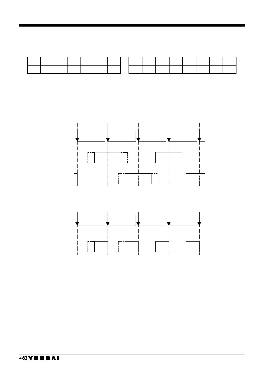
HM17CM256
- 75 -
relation with Y address setting value.
To access with DMY = "1", register data write-in is possible with increment mode.
(34-31) PWM mode control
CS RS RD WR RE
2
RE
1
RE
0
D
7
D
6
D
5
D
4
D
3
D
2
D
1
D
0
0
1
1
0
1
0
1
1
0
1
0
PWMS
PWMA
PWMB
PWMC
( reset :{PWMS, PWMA, PWMB, PWMC}=0
H
, read address :8
H
)
* : "Don't care"
PWM mode selection. ( Refer to following wave diagram. )
PWMS="0": Selection PWM type1.
PWMA, PWMB, PWMC="0" : PWM type1-O is selectable for each A, B, C data.
PWMA, PWMB, PWMC="1" : PWM type1-E is selectable for each A, B, C data.
PWMS="1": Selection PWM type2.
a) PWM type1 (PWMS="0")
b) PWM type2 (PWMS="1")
odd line
even line
�
�
�
�
"H"
"L"
V
LCD
V
2
V
2
Type-O
Type-E
CL
SEG
V
LCD
�
"H"
"L"
CL
SEG
�
V
2
V
LCD

HM17CM256
- 76 -
(35) Relation between each setting and COM / display RAM
The COM port number corresponds to Y address of display RAM by SHIFT command, LCD duty
command, common display start position command and display start line setting command.
�
When display start address was set to "0".
According to LCD duty and display start common line address, the port of COM line and
display RAM address ( MY ) is changed by 15 line unit.
When SHIFT register is set to "0" common line shift to upward direction, and when the value is
"1", common line shift to downward direction. When display start address (LA
6
~LA
0
) is set to
"0", the "MY" corresponds to starting position is "0". The MY shift upward direction as display
goes on.
In any case, COMI
0
=MY80, COMI
1
=MY81 .
�
When display start line was set except for "0"
According to LCD duty and display start common line address, the port of COM line and
display RAM address, MY is changed by 15 line unit.
When SHIFT register is set to "0" common line shift to upward direction, and when the value is
"1", common line shift to downward direction. When display start address (LA
6
~LA
0
) is set to
except for "0", the "MY" corresponds to starting position is shift by the amount of set value.
The MY shift upward direction as display goes on but MY is set to "0" after MY=79.
In any case, COMI
0
=MY80, COMI
1
=MY81 .
HM17CM256
- 77 -
�
display start line set to "0" , 1/82 duty by DS
2
~DS
0
register
SHIFT set value
SHIFT="0" (common forward scan)
SHIFT="1" (common backward scan)
DS
2
DS
1
DS
0
"000" (1/82 duty)
"000" (1/82 duty)
SC
2
SC
1
SC
0
"000"
"001"
"010"
"011"
"100"
"101"
"000"
"001"
"010"
"011"
"100"
"101"
LA
6
�
�
�
�
�
�
�
�
LA
0
"0000000" (display start point 0)
"0000000" (display start point 0)
COMI
0
80
80
80
80
80
80
80
80
80
80
80
80
COM
0
0
65
50
35
20
5
79
64
49
34
19
4
COM
1
COM
2
COM
3
COM
4
0
COM
5
79
COM
6
COM
7
COM
8
COM
9
COM
10
COM
11
COM
12
COM
13
COM
14
79
COM
15
0
COM
16
COM
17
COM
18
COM
19
0
COM
20
79
COM
21
COM
22
COM
23
COM
24
COM
25
COM
26
COM
27
COM
28
COM
29
79
COM
30
0
COM
31
COM
32
COM
33
COM
34
0
COM
35
79
COM
36
COM
37
COM
38
COM
39
COM
40
COM
41
COM
42
COM
43
COM
44
79
COM
45
0
COM
46
COM
47
COM
48
COM
49
0
COM
50
79
COM
51
COM
52
COM
53
COM
54
COM
55
COM
56
COM
57
COM
58
COM
59
79
COM
60
0
COM
61
COM
62
COM
63
COM
64
0
COM
65
79
COM
66
COM
67
COM
68
COM
69
COM
70
COM
71
COM
72
COM
73
COM
74
79
COM
75
0
COM
76
COM
77
COM
78
COM
79
79
64
49
34
19
4
0
65
50
35
20
5
COMI
1
81
81
81
81
81
81
81
81
81
81
81
81
The number on the table means MY ( Y direction shift address ).
The COM electrodes without MY number are driving with non-selection level signal.
The Marked line is display start line.

HM17CM256
- 78 -
�
display start line set to "0" , 1/77 duty by DS
2
~DS
0
register
SHIFT set value
SHIFT="0" (common forward scan)
SHIFT="1" (common backward scan)
DS
2
DS
1
DS
0
"001" (1/77 duty)
"001" (1/77 duty)
SC
2
SC
1
SC
0
"000"
"001"
"010"
"011"
"100"
"101"
"000"
"001"
"010"
"011"
"100"
"101"
LA
6
�
�
�
�
�
�
�
�
LA
0
"0000000" (display start point 0)
"0000000" (display start point 0)
COMI
0
80
80
80
80
80
80
80
80
80
80
80
80
COM
0
0
65
50
35
20
5
64
49
34
19
4
COM
1
COM
2
COM
3
COM
4
0
COM
5
74
COM
6
COM
7
COM
8
COM
9
74
COM
10
74
COM
11
COM
12
COM
13
COM
14
COM
15
0
COM
16
COM
17
COM
18
COM
19
0
COM
20
COM
21
COM
22
COM
23
COM
24
74
COM
25
74
COM
26
COM
27
COM
28
COM
29
COM
30
0
COM
31
COM
32
COM
33
COM
34
0
COM
35
COM
36
COM
37
COM
38
COM
39
74
COM
40
74
COM
41
COM
42
COM
43
COM
44
COM
45
0
COM
46
COM
47
COM
48
COM
49
0
COM
50
COM
51
COM
52
COM
53
COM
54
74
COM
55
74
COM
56
COM
57
COM
58
COM
59
COM
60
0
COM
61
COM
62
COM
63
COM
64
0
COM
65
COM
66
COM
67
COM
68
COM
69
74
COM
70
74
COM
71
COM
72
COM
73
COM
74
74
COM
75
0
COM
76
COM
77
COM
78
COM
79
64
49
34
19
4
0
65
50
35
20
5
COMI
1
81
81
81
81
81
81
81
81
81
81
81
81
The number on the table means MY ( Y direction shift address ).
The COM electrodes without MY number are driving with non-selection level signal.
The Marked line is display start line.

HM17CM256
- 79 -
�
display start line set to "0" , 1/66 duty by DS
2
~DS
0
register
SHIFT set value
SHIFT="0" (common forward scan)
SHIFT="1" (common backward scan)
DS
2
DS
1
DS
0
"010" (1/66 duty)
"010" (1/66 duty)
SC
2
SC
1
SC
0
"000"
"001"
"010"
"011"
"100"
"101"
"000"
"001"
"010"
"011"
"100"
"101"
LA
6
�
�
�
�
�
�
�
�
LA
0
"0000000" (display start point 0)
"0000000" (display start point 0)
COMI
0
80
80
80
80
80
80
80
80
80
80
80
80
COM
0
0
50
35
20
5
49
34
19
4
COM
1
63
COM
2
COM
3
COM
4
0
COM
5
COM
6
COM
7
COM
8
COM
9
COM
10
COM
11
COM
12
COM
13
63
COM
14
COM
15
0
COM
16
63
COM
17
COM
18
COM
19
0
COM
20
COM
21
63
COM
22
COM
23
COM
24
COM
25
COM
26
COM
27
COM
28
63
COM
29
COM
30
0
COM
31
COM
32
COM
33
COM
34
0
COM
35
COM
36
63
COM
37
COM
38
COM
39
COM
40
COM
41
COM
42
COM
43
63
COM
44
COM
45
0
COM
46
COM
47
COM
48
COM
49
0
COM
50
COM
51
63
COM
52
COM
53
COM
54
COM
55
COM
56
COM
57
COM
58
63
COM
59
COM
60
0
COM
61
COM
62
COM
63
63
COM
64
0
COM
65
COM
66
63
COM
67
COM
68
COM
69
COM
70
COM
71
COM
72
COM
73
COM
74
COM
75
0
COM
76
COM
77
COM
78
63
COM
79
49
34
19
4
0
50
35
20
5
COMI
1
81
81
81
81
81
81
81
81
81
81
81
81
The number on the table means MY ( Y direction shift address ).
The COM electrodes without MY number are driving with non-selection level signal.
The Marked line is display start line.

HM17CM256
- 80 -
�
display start line set to "0" , 1/47 duty by DS
2
~DS
0
register
SHIFT set value
SHIFT="0" (common forward scan)
SHIFT="1" (common backward scan)
DS
2
DS
1
DS
0
"011" (1/47 duty)
"011" (1/47 duty)
SC
2
SC
1
SC
0
"000"
"001"
"010"
"011"
"100"
"101"
"000"
"001"
"010"
"011"
"100"
"101"
LA
6
�
�
�
�
�
�
�
�
LA
0
"0000000" (display start point 0)
"0000000" (display start point 0)
COMI
0
80
80
80
80
80
80
80
80
80
80
80
80
COM
0
0
35
20
5
34
19
4
COM
1
COM
2
COM
3
COM
4
0
COM
5
44
COM
6
COM
7
COM
8
COM
9
44
COM
10
COM
11
COM
12
COM
13
COM
14
COM
15
0
COM
16
COM
17
COM
18
COM
19
0
COM
20
44
COM
21
COM
22
COM
23
COM
24
44
COM
25
COM
26
COM
27
COM
28
COM
29
COM
30
0
COM
31
COM
32
COM
33
COM
34
0
COM
35
44
COM
36
COM
37
COM
38
COM
39
44
COM
40
44
COM
41
COM
42
COM
43
COM
44
44
COM
45
0
COM
46
COM
47
COM
48
COM
49
0
COM
50
COM
51
COM
52
COM
53
COM
54
COM
55
44
COM
56
COM
57
COM
58
COM
59
44
COM
60
0
COM
61
COM
62
COM
63
COM
64
0
COM
65
COM
66
COM
67
COM
68
COM
69
COM
70
44
COM
71
COM
72
COM
73
COM
74
44
COM
75
0
COM
76
COM
77
COM
78
COM
79
34
19
4
0
35
20
5
COMI
1
81
81
81
81
81
81
81
81
81
81
81
81
The number on the table means MY ( Y direction shift address ).
The COM electrodes without MY number are driving with non-selection level signal.
The Marked line is display start line.
HM17CM256
- 81 -
�
display start line set to "0" , 1/32 duty by DS
2
~DS
0
register
SHIFT set value
SHIFT="0" (common forward scan)
SHIFT="1" (common back scan)
DS
2
DS
1
DS
0
"100" (1/32 duty)
"100" (1/32 duty)
SC
2
SC
1
SC
0
"000"
"001"
"010"
"011"
"100"
"101"
"000"
"001"
"010"
"011"
"100"
"101"
LA
6
�
�
�
�
�
�
�
�
LA
0
"0000000" (display start point 0)
"0000000" (display start point 0)
COMI
0
80
80
80
80
80
80
80
80
80
80
80
80
COM
0
0
20
5
19
4
COM
1
COM
2
COM
3
COM
4
0
COM
5
29
COM
6
COM
7
COM
8
COM
9
29
COM
10
COM
11
COM
12
COM
13
COM
14
COM
15
0
COM
16
COM
17
COM
18
COM
19
0
COM
20
29
COM
21
COM
22
COM
23
COM
24
29
COM
25
COM
26
COM
27
COM
28
COM
29
29
COM
30
0
COM
31
COM
32
COM
33
COM
34
0
COM
35
29
COM
36
COM
37
COM
38
COM
39
COM
40
COM
41
COM
42
COM
43
COM
44
29
COM
45
0
COM
46
COM
47
COM
48
COM
49
0
COM
50
29
COM
51
COM
52
COM
53
COM
54
COM
55
29
COM
56
COM
57
COM
58
COM
59
29
COM
60
0
COM
61
COM
62
COM
63
COM
64
0
COM
65
COM
66
COM
67
COM
68
COM
69
COM
70
29
COM
71
COM
72
COM
73
COM
74
29
COM
75
0
COM
76
COM
77
COM
78
COM
79
19
4
0
20
5
COMI
1
81
81
81
81
81
81
81
81
81
81
81
81
The number on the table means MY ( Y direction shift address ).
The COM electrodes without MY number are driving with non-selection level signal.
The Marked line is display start line.

HM17CM256
- 82 -
�
display start line set to "0" , 1/17 duty by DS
2
~DS
0
register
SHIFT set value
SHIFT="0" (common forward scan)
SHIFT="1" (common backward scan)
DS
2
DS
1
DS
0
"101" (1/17 duty)
"101" (1/17 duty)
SC
2
SC
1
SC
0
"000"
"001"
"010"
"011"
"100"
"101"
"000"
"001"
"010"
"011"
"100"
"101"
LA
6
�
�
�
�
�
�
�
�
LA
0
"0000000" (display start point 0)
"0000000" (display start point 0)
COMI
0
80
80
80
80
80
80
80
80
80
80
80
80
COM
0
0
5
4
COM
1
COM
2
COM
3
COM
4
0
COM
5
14
COM
6
COM
7
COM
8
COM
9
14
COM
10
COM
11
COM
12
COM
13
COM
14
14
COM
15
0
COM
16
COM
17
COM
18
COM
19
0
COM
20
14
COM
21
COM
22
COM
23
COM
24
COM
25
COM
26
COM
27
COM
28
COM
29
14
COM
30
0
COM
31
COM
32
COM
33
COM
34
0
COM
35
14
COM
36
COM
37
COM
38
COM
39
COM
40
COM
41
COM
42
COM
43
COM
44
14
COM
45
0
COM
46
COM
47
COM
48
COM
49
0
COM
50
14
COM
51
COM
52
COM
53
COM
54
COM
55
COM
56
COM
57
COM
58
COM
59
14
COM
60
0
COM
61
COM
62
COM
63
COM
64
0
COM
65
14
COM
66
COM
67
COM
68
COM
69
COM
70
14
COM
71
COM
72
COM
73
COM
74
14
COM
75
0
COM
76
COM
77
COM
78
COM
79
4
0
5
COMI
1
81
81
81
81
81
81
81
81
81
81
81
81
The number on the table means MY ( Y direction shift address ).
The COM electrodes without MY number are driving with non-selection level signal.
The Marked line is display start line.
HM17CM256
- 83 -
�
display start line set to "0" , 1/38 duty by DS
2
~DS
0
register
SHIFT set value
SHIFT="0" (common forward scan)
SHIFT="1" (common backward scan)
DS
2
DS
1
DS
0
"110" (1/38 duty)
"110" (1/38 duty)
SC
2
SC
1
SC
0
"000"
"001"
"010"
"011"
"100"
"101"
"000"
"001"
"010"
"011"
"100"
"101"
LA
6
�
�
�
�
�
�
�
�
LA
0
"0000000" (display start point 0)
"0000000" (display start point 0)
COMI
0
80
80
80
80
80
80
80
80
80
80
80
80
COM
0
0
35
20
5
34
19
4
COM
1
COM
2
COM
3
COM
4
0
COM
5
COM
6
COM
7
COM
8
COM
9
COM
10
COM
11
COM
12
COM
13
COM
14
35
COM
15
0
35
COM
16
COM
17
COM
18
COM
19
0
COM
20
COM
21
COM
22
COM
23
COM
24
COM
25
COM
26
COM
27
COM
28
COM
29
35
COM
30
0
35
COM
31
COM
32
COM
33
COM
34
0
COM
35
35
COM
36
COM
37
COM
38
COM
39
COM
40
COM
41
COM
42
COM
43
COM
44
35
COM
45
0
COM
46
COM
47
COM
48
COM
49
0
35
COM
50
35
COM
51
COM
52
COM
53
COM
54
COM
55
COM
56
COM
57
COM
58
COM
59
COM
60
0
COM
61
COM
62
COM
63
COM
64
0
35
COM
65
35
COM
66
COM
67
COM
68
COM
69
COM
70
COM
71
COM
72
COM
73
COM
74
COM
75
0
COM
76
COM
77
COM
78
COM
79
34
19
4
0
35
20
5
COMI
1
81
81
81
81
81
81
81
81
81
81
81
81
The number on the table means MY ( Y direction shift address ).
The COM electrodes without MY number are driving with non-selection level signal.
The Marked line is display start line.
HM17CM256
- 84 -
�
display start line set to "0" , 1/26 duty by DS
2
~DS
0
register
SHIFT set value
SHIFT="0" (common forward scan)
SHIFT="1" (common backward scan)
DS
2
DS
1
DS
0
"111" (1/26 duty)
"111" (1/26 duty)
SC
2
SC
1
SC
0
"000"
"001"
"010"
"011"
"100"
"101"
"000"
"001"
"010"
"011"
"100"
"101"
LA
6
�
�
�
�
�
�
�
�
LA
0
"0000000" (display start point 0)
"0000000" (display start point 0)
COMI
0
80
80
80
80
80
80
80
80
80
80
80
80
COM
0
0
20
5
19
4
COM
1
COM
2
COM
3
23
COM
4
0
COM
5
COM
6
COM
7
COM
8
COM
9
COM
10
COM
11
23
COM
12
COM
13
COM
14
COM
15
0
COM
16
COM
17
COM
18
23
COM
19
0
COM
20
COM
21
COM
22
COM
23
23
COM
24
COM
25
COM
26
23
COM
27
COM
28
COM
29
COM
30
0
COM
31
COM
32
COM
33
COM
34
0
COM
35
COM
36
COM
37
COM
38
23
COM
39
COM
40
COM
41
23
COM
42
COM
43
COM
44
COM
45
0
COM
46
COM
47
COM
48
COM
49
0
COM
50
COM
51
COM
52
COM
53
23
COM
54
COM
55
COM
56
23
COM
57
COM
58
COM
59
COM
60
0
COM
61
23
COM
62
COM
63
COM
64
0
COM
65
COM
66
COM
67
COM
68
23
COM
69
COM
70
COM
71
COM
72
COM
73
COM
74
COM
75
0
COM
76
23
COM
77
COM
78
COM
79
19
4
0
20
5
COMI
1
81
81
81
81
81
81
81
81
81
81
81
81
The number on the table means MY ( Y direction shift address ).
The COM electrodes without MY number are driving with non-selection level signal.
The Marked line is display start line.

HM17CM256
- 85 -
�
display start line set to "5" , 1/82 duty by DS
2
~DS
0
register
SHIFT set value
SHIFT="0" (common forward scan)
SHIFT="1" (common backward scan)
DS
2
DS
1
DS
0
"000" (1/82 duty)
"000" (1/82 duty)
SC
2
SC
1
SC
0
"000"
"001"
"010"
"011"
"100"
"101"
"000"
"001"
"010"
"011"
"100"
"101"
LA
6
�
�
�
�
�
�
�
�
LA
0
"0000101" (display start point 5)
"0000101" (display start point 5)
COMI
0
80
80
80
80
80
80
80
80
80
80
80
80
COM
0
5
70
55
40
25
10
4
69
54
39
24
9
COM
1
COM
2
COM
3
COM
4
0
5
COM
5
79
COM
6
COM
7
COM
8
COM
9
79
0
COM
10
0
79
COM
11
COM
12
COM
13
COM
14
COM
15
5
COM
16
COM
17
COM
18
COM
19
5
COM
20
COM
21
COM
22
COM
23
COM
24
79
0
COM
25
0
79
COM
26
COM
27
COM
28
COM
29
COM
30
5
COM
31
COM
32
COM
33
COM
34
5
COM
35
COM
36
COM
37
COM
38
COM
39
79
0
COM
40
0
79
COM
41
COM
42
COM
43
COM
44
COM
45
5
COM
46
COM
47
COM
48
COM
49
5
COM
50
COM
51
COM
52
COM
53
COM
54
79
0
COM
55
0
79
COM
56
COM
57
COM
58
COM
59
COM
60
5
COM
61
COM
62
COM
63
COM
64
5
COM
65
COM
66
COM
67
COM
68
COM
69
79
0
COM
70
0
79
COM
71
COM
72
COM
73
COM
74
79
COM
75
0
5
COM
76
COM
77
COM
78
COM
79
4
69
54
39
24
9
5
70
55
40
25
10
COMI
1
81
81
81
81
81
81
81
81
81
81
81
81
The number on the table means MY ( Y direction shift address ).
The COM electrodes without MY number are driving with non-selection level signal.
The Marked line is display start line.
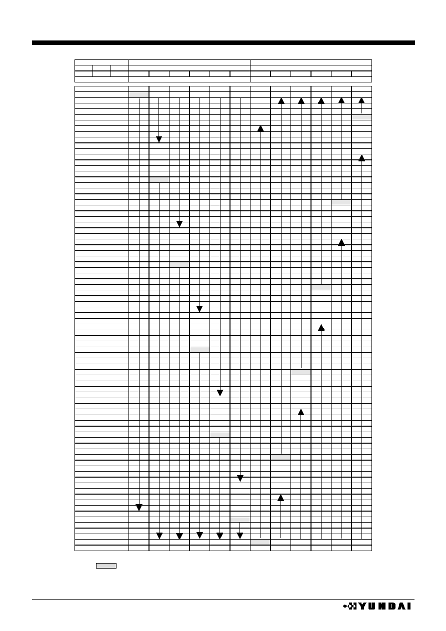
HM17CM256
- 86 -
�
display start line set to "5" , 1/77 duty by DS
2
~DS
0
register
SHIFT set value
SHIFT="0" (common forward scan)
SHIFT="1" (common backward scan)
DS
2
DS
1
DS
0
"001" (1/77 duty)
"001" (1/77 duty)
SC
2
SC
1
SC
0
"000"
"001"
"010"
"011"
"100"
"101"
"000"
"001"
"010"
"011"
"100"
"101"
LA
6
�
�
�
�
�
�
�
�
LA
0
"0000101" (display start point 5)
"0000101" (display start point 5)
COMI
0
80
80
80
80
80
80
80
80
80
80
80
80
COM
0
5
70
55
40
25
10
69
54
39
24
9
COM
1
COM
2
COM
3
COM
4
5
COM
5
79
COM
6
COM
7
COM
8
COM
9
79
COM
10
79
COM
11
COM
12
COM
13
COM
14
COM
15
5
COM
16
COM
17
COM
18
COM
19
5
COM
20
COM
21
COM
22
COM
23
COM
24
79
COM
25
79
COM
26
COM
27
COM
28
COM
29
COM
30
5
COM
31
COM
32
COM
33
COM
34
5
COM
35
COM
36
COM
37
COM
38
COM
39
79
COM
40
79
COM
41
COM
42
COM
43
COM
44
COM
45
5
COM
46
COM
47
COM
48
COM
49
5
COM
50
COM
51
COM
52
COM
53
COM
54
79
COM
55
79
COM
56
COM
57
COM
58
COM
59
COM
60
5
COM
61
COM
62
COM
63
COM
64
5
COM
65
COM
66
COM
67
COM
68
COM
69
79
COM
70
79
COM
71
COM
72
COM
73
COM
74
79
COM
75
5
COM
76
COM
77
COM
78
COM
79
69
54
39
24
9
5
70
55
40
25
10
COMI
1
81
81
81
81
81
81
81
81
81
81
81
81
The number on the table means MY ( Y direction shift address ).
The COM electrodes without MY number are driving with non-selection level signal.
The Marked line is display start line.
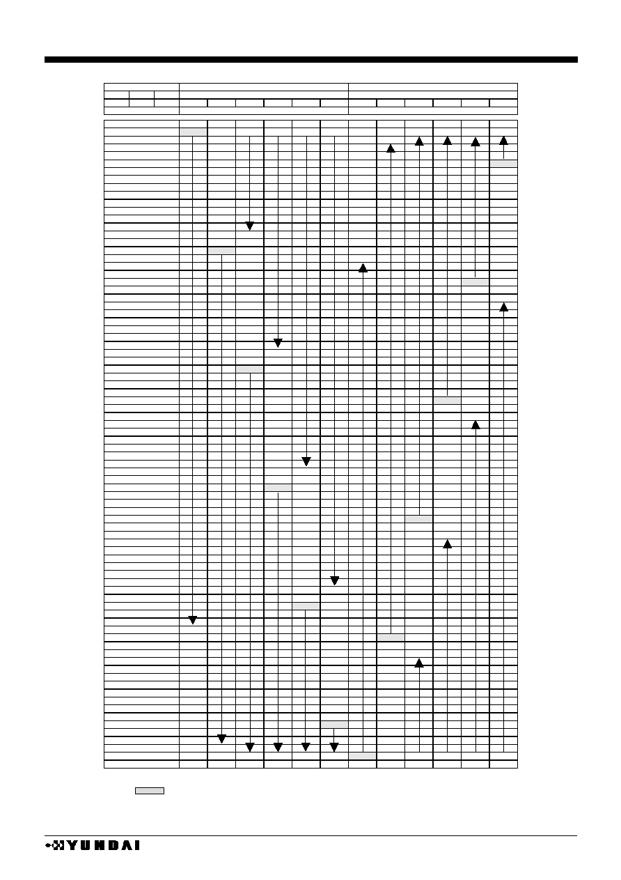
HM17CM256
- 87 -
�
display start line set to "5" , 1/66 duty by DS
2
~DS
0
register
SHIFT set value
SHIFT="0" (common forward scan)
SHIFT="1" (common backward scan)
DS
2
DS
1
DS
0
"010" (1/66 duty)
"010" (1/66 duty)
SC
2
SC
1
SC
0
"000"
"001"
"010"
"011"
"100"
"101"
"000"
"001"
"010"
"011"
"100"
"101"
LA
6
�
�
�
�
�
�
�
�
LA
0
"0000101" (display start point 5)
"0000101" (display start point 5)
COMI
0
80
80
80
80
80
80
80
80
80
80
80
80
COM
0
5
55
40
25
10
54
39
24
9
COM
1
68
COM
2
COM
3
COM
4
5
COM
5
COM
6
COM
7
COM
8
COM
9
COM
10
COM
11
COM
12
COM
13
68
COM
14
COM
15
5
COM
16
68
COM
17
COM
18
COM
19
5
COM
20
COM
21
68
COM
22
COM
23
COM
24
COM
25
COM
26
COM
27
COM
28
68
COM
29
COM
30
5
COM
31
COM
32
COM
33
COM
34
5
COM
35
COM
36
68
COM
37
COM
38
COM
39
COM
40
COM
41
COM
42
COM
43
68
COM
44
COM
45
5
COM
46
COM
47
COM
48
COM
49
5
COM
50
COM
51
68
COM
52
COM
53
COM
54
COM
55
COM
56
COM
57
COM
58
68
COM
59
COM
60
5
COM
61
COM
62
COM
63
68
COM
64
5
COM
65
COM
66
68
COM
67
COM
68
COM
69
COM
70
COM
71
COM
72
COM
73
COM
74
COM
75
5
COM
76
COM
77
COM
78
68
COM
79
54
39
24
9
5
55
40
25
10
COMI
1
81
81
81
81
81
81
81
81
81
81
81
81
The number on the table means MY ( Y direction shift address ).
The COM electrodes without MY number are driving with non-selection level signal.
The Marked line is display start line.
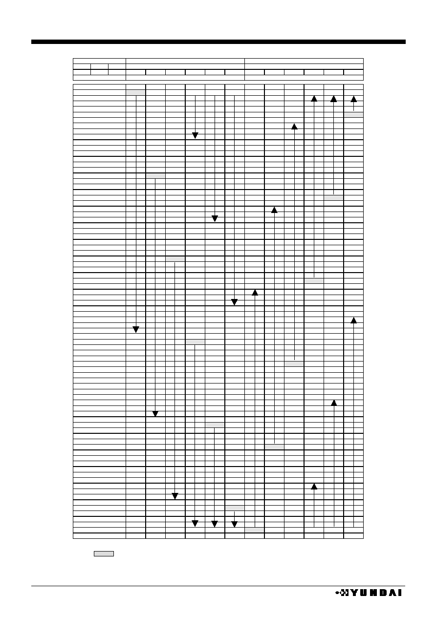
HM17CM256
- 88 -
�
display start line set to "5" , 1/47 duty by DS
2
~DS
0
register
SHIFT set value
SHIFT="0" (common forward scan)
SHIFT="1" (common backward scan)
DS
2
DS
1
DS
0
"011" (1/47 duty)
"011" (1/47 duty)
SC
2
SC
1
SC
0
"000"
"001"
"010"
"011"
"100"
"101"
"000"
"001"
"010"
"011"
"100"
"101"
LA
6
�
�
�
�
�
�
�
�
LA
0
"0000101" (display start point 5)
"0000101" (display start point 5)
COMI
0
80
80
80
80
80
80
80
80
80
80
80
80
COM
0
5
40
25
10
39
24
9
COM
1
COM
2
COM
3
COM
4
5
COM
5
49
COM
6
COM
7
COM
8
COM
9
49
COM
10
COM
11
COM
12
COM
13
COM
14
COM
15
5
COM
16
COM
17
COM
18
COM
19
5
COM
20
49
COM
21
COM
22
COM
23
COM
24
49
COM
25
COM
26
COM
27
COM
28
COM
29
COM
30
5
COM
31
COM
32
COM
33
COM
34
5
COM
35
49
COM
36
COM
37
COM
38
COM
39
49
COM
40
49
COM
41
COM
42
COM
43
COM
44
49
COM
45
5
COM
46
COM
47
COM
48
COM
49
5
COM
50
COM
51
COM
52
COM
53
COM
54
COM
55
49
COM
56
COM
57
COM
58
COM
59
49
COM
60
5
COM
61
COM
62
COM
63
COM
64
5
COM
65
COM
66
COM
67
COM
68
COM
69
COM
70
49
COM
71
COM
72
COM
73
COM
74
49
COM
75
5
COM
76
COM
77
COM
78
COM
79
39
24
9
5
40
25
10
COMI
1
81
81
81
81
81
81
81
81
81
81
81
81
The number on the table means MY ( Y direction shift address ).
The COM electrodes without MY number are driving with non-selection level signal.
The Marked line is display start line.

HM17CM256
- 89 -
�
display start line set to "5" , 1/32 duty by DS
2
~DS
0
register
SHIFT set value
SHIFT="0" (common forward scan)
SHIFT="1" (common backward scan)
DS
2
DS
1
DS
0
"100" (1/32 duty)
"100" (1/32 duty)
SC
2
SC
1
SC
0
"000"
"001"
"010"
"011"
"100"
"101"
"000"
"001"
"010"
"011"
"100"
"101"
LA
6
�
�
�
�
�
�
�
�
LA
0
"0000101" (display start point 5)
"0000101" (display start point 5)
COMI
0
80
80
80
80
80
80
80
80
80
80
80
80
COM
0
5
25
10
24
9
COM
1
COM
2
COM
3
COM
4
5
COM
5
34
COM
6
COM
7
COM
8
COM
9
34
COM
10
COM
11
COM
12
COM
13
COM
14
COM
15
5
COM
16
COM
17
COM
18
COM
19
5
COM
20
34
COM
21
COM
22
COM
23
COM
24
34
COM
25
COM
26
COM
27
COM
28
COM
29
34
COM
30
5
COM
31
COM
32
COM
33
COM
34
5
COM
35
34
COM
36
COM
37
COM
38
COM
39
COM
40
COM
41
COM
42
COM
43
COM
44
34
COM
45
5
COM
46
COM
47
COM
48
COM
49
5
COM
50
34
COM
51
COM
52
COM
53
COM
54
COM
55
34
COM
56
COM
57
COM
58
COM
59
34
COM
60
5
COM
61
COM
62
COM
63
COM
64
5
COM
65
COM
66
COM
67
COM
68
COM
69
COM
70
34
COM
71
COM
72
COM
73
COM
74
34
COM
75
5
COM
76
COM
77
COM
78
COM
79
24
9
5
25
10
COMI
1
81
81
81
81
81
81
81
81
81
81
81
81
The number on the table means MY ( Y direction shift address ).
The COM electrodes without MY number are driving with non-selection level signal.
The Marked line is display start line.

HM17CM256
- 90 -
�
display start line set to "5" , 1/17 duty by DS
2
~DS
0
register
SHIFT set value
SHIFT="0" (common forward scan)
SHIFT="1" (common backward scan)
DS
2
DS
1
DS
0
"101" (1/17 duty)
"101" (1/17 duty)
SC
2
SC1
SC
0
"000"
"001"
"010"
"011"
"100"
"101"
"000"
"001"
"010"
"011"
"100"
"101"
LA
6
�
�
�
�
�
�
�
�
LA
0
"0000101" (display start point 5)
"0000101" (display start point 5)
COMI
0
80
80
80
80
80
80
80
80
80
80
80
80
COM
0
5
10
9
COM
1
COM
2
COM
3
COM
4
5
COM
5
19
COM
6
COM
7
COM
8
COM
9
19
COM
10
COM
11
COM
12
COM
13
COM
14
19
COM
15
5
COM
16
COM
17
COM
18
COM
19
5
COM
20
19
COM
21
COM
22
COM
23
COM
24
COM
25
COM
26
COM
27
COM
28
COM
29
19
COM
30
5
COM
31
COM
32
COM
33
COM
34
5
COM
35
19
COM
36
COM
37
COM
38
COM
39
COM
40
COM
41
COM
42
COM
43
COM
44
19
COM
45
5
COM
46
COM
47
COM
48
COM
49
5
COM
50
19
COM
51
COM
52
COM
53
COM
54
COM
55
COM
56
COM
57
COM
58
COM
59
19
COM
60
5
COM
61
COM
62
COM
63
COM
64
5
COM
65
19
COM
66
COM
67
COM
68
COM
69
COM
70
19
COM
71
COM
72
COM
73
COM
74
19
COM
75
5
COM
76
COM
77
COM
78
COM
79
9
5
10
COMI
1
81
81
81
81
81
81
81
81
81
81
81
81
The number on the table means MY ( Y direction shift address ).
The COM electrodes without MY number are driving with non-selection level signal.
The Marked line is display start line.

HM17CM256
- 91 -
�
display start line set to "5" , 1/38 duty by DS
2
~DS
0
register
SHIFT set value
SHIFT="0" (common forward scan)
SHIFT="1" (common backward scan)
DS
2
DS
1
DS
0
"110" (1/38 duty)
"110" (1/38 duty)
SC
2
SC
1
SC
0
"000"
"001"
"010"
"011"
"100"
"101"
"000"
"001"
"010"
"011"
"100"
"101"
LA
6
�
�
�
�
�
�
�
�
LA
0
"0000101" (display start point 5)
"0000101" (display start point 5)
COMI
0
80
80
80
80
80
80
80
80
80
80
80
80
COM
0
5
40
25
10
39
24
9
COM
1
COM
2
COM
3
COM
4
5
COM
5
COM
6
COM
7
COM
8
COM
9
COM
10
COM
11
COM
12
COM
13
COM
14
40
COM
15
5
40
COM
16
COM
17
COM
18
COM
19
5
COM
20
COM
21
COM
22
COM
23
COM
24
COM
25
COM
26
COM
27
COM
28
COM
29
40
COM
30
5
40
COM
31
COM
32
COM
33
COM
34
5
COM
35
40
COM
36
COM
37
COM
38
COM
39
COM
40
COM
41
COM
42
COM
43
COM
44
40
COM
45
5
COM
46
COM
47
COM
48
COM
49
5
40
COM
50
40
COM
51
COM
52
COM
53
COM
54
COM
55
COM
56
COM
57
COM
58
COM
59
COM
60
5
COM
61
COM
62
COM
63
COM
64
5
40
COM
65
40
COM
66
COM
67
COM
68
COM
69
COM
70
COM
71
COM
72
COM
73
COM
74
COM
75
5
COM
76
COM
77
COM
78
COM
79
39
24
9
5
40
25
10
COMI
1
81
81
81
81
81
81
81
81
81
81
81
81
The number on the table means MY ( Y direction shift address ).
The COM electrodes without MY number are driving with non-selection level signal.
The Marked line is display start line.

HM17CM256
- 92 -
�
display start line set to "5" , 1/26 duty by DS
2
~DS
0
register
SHIFT set value
SHIFT="0" (common forward scan)
SHIFT="1" (common backward scan)
DS
2
DS
1
DS
0
"111" (1/26 duty)
"111" (1/26 duty)
SC
2
SC
1
SC
0
"000"
"001"
"010"
"011"
"100"
"101"
"000"
"001"
"010"
"011"
"100"
"101"
LA
6
�
�
�
�
�
�
�
�
LA
0
"0000101" (display start point 5)
"0000101" (display start point 5)
COMI
0
80
80
80
80
80
80
80
80
80
80
80
80
COM
0
5
25
10
24
9
COM
1
COM
2
COM
3
28
COM
4
5
COM
5
COM
6
COM
7
COM
8
COM
9
COM
10
COM
11
28
COM
12
COM
13
COM
14
COM
15
5
COM
16
COM
17
COM
18
28
COM
19
5
COM
20
COM
21
COM
22
COM
23
28
COM
24
COM
25
COM
26
28
COM
27
COM
28
COM
29
COM
30
5
COM
31
COM
32
COM
33
COM
34
5
COM
35
COM
36
COM
37
COM
38
28
COM
39
COM
40
COM
41
28
COM
42
COM
43
COM
44
COM
45
5
COM
46
COM
47
COM
48
COM
49
5
COM
50
COM
51
COM
52
COM
53
28
COM
54
COM
55
COM
56
28
COM
57
COM
58
COM
59
COM
60
5
COM
61
28
COM
62
COM
63
COM
64
5
COM
65
COM
66
COM
67
COM
68
28
COM
69
COM
70
COM
71
COM
72
COM
73
COM
74
COM
75
5
COM
76
28
COM
77
COM
78
COM
79
24
9
5
25
10
COMI
1
81
81
81
81
81
81
81
81
81
81
81
81
The number on the table means MY ( Y direction shift address ).
The COM electrodes without MY number are driving with non-selection level signal.
The Marked line is display start line.

HM17CM256
- 93 -
s
ABSOLUTE MAXIMUM RATING
ITEM
SYMBOL
CONDITION
PORT
RATINGS
UNIT
supply voltage (1)
V
DD
V
DD
-0.3 ~ +4.0
V
supply voltage (2)
V
EE
V
EE
-0.3 ~ +4.0
V
supply voltage (3)
V
OUT
V
OUT
-0.3 ~ +20.0
V
supply voltage (4)
V
REG
V
REG
-0.3 ~ +20.0
V
supply voltage (5)
V
LCD
V
LCD
-0.3 ~ +20.0
V
supply voltage (6) V
1,
V
2,
V
3,
V
4
V
1,
V
2,
V
3,
V
4
-0.3 ~ V
LCD
+ 0.3
V
input voltage
V
I
V
SS
(0V)
reference
Ta = +25
�
C
*1
-0.3 ~ V
DD
+ 0.3
V
Storage temperature
T
stg
-45 ~ +125
�
C
*1 D
0
~D
15
, CS, RS, M/S, RD, WR, OSC
1
, LP, FLM, FR, CLK, RES, TEST port
s
RECOMMENDED OPERATING CONDITIONS
ITEM
SYMBOL
PORT
MIN
TYP
MAX
UNIT REMARK
V
DD1
1.7
3.3
V
*1
V
DD2
V
DD
2.4
3.3
V
*2
supply voltage
V
EE
V
EE
2.4
3.3
V
*3
V
LCD
V
LCD
5
18.0
V
*4
V
OUT
V
OUT
18.0
V
V
REG
V
REG
V
OUT
x 0.9 V
Recommended
operating voltage
V
REF
V
REF
2.1
3.3
V
*5
Operation
temperature
T
opr
-30
85
�
C
*1 The case when internal reference voltage generation circuit (V
BA
output) is not used.
The voltage compare to V
SS
port.
*2 The case when internal reference voltage generation circuit (V
BA
output) is used.
The voltage compare to V
SS
port.
*3 When the boosting circuit is used, supply voltage V
EE
should be used within the limit.
When driving LCD panel by use of internal boosting circuit, it is possible to short V
DD
and V
EE
.
*4 Please keep the relation, V
SS
< V
4
< V
3
< V
2
< V
1
< V
LCD
V
OUT
.
*5 When the internal voltage regulator circuit is used, reference voltage V
REF
should be used within the limit.
Please keep the relation V
REF
V
EE
.

HM17CM256
- 94 -
s
ELECTRICAL CHARACTERISTICS
�
DC Characteristics 1
Unless otherwise noted V
SS
= 0V, V
DD
= +1.7~+3.3V, Ta = -30~+85
�
C
ITEM
SYMBOL
CONDITION
MIN
TYP
MAX
UNIT PORT
High level input voltage
V
IH
0.8 V
DD
V
DD
V
*1
Low level input voltage
V
IL
0
0.22 V
DD
V
*1
High level output voltage
V
OH1
I
OH
= -0.4mA
V
DD
- 0.4
V
*2
Low level output voltage
V
OL1
I
OL
= 0.4mA
0.4
V
*2
High level output voltage
V
OH2
I
OH
= -0.1mA
V
DD
- 0.4
V
*3
Low level output voltage
V
OL2
I
OL
= 0.1mA
0.4
V
*3
Input leakage current
IL
I
V
I
= V
SS
or V
DD
-10
10
�
A
*4
Output leakage current
IL
O
V
I
= V
SS
or V
DD
-10
10
�
A
*5
V
LCD
= 10V
1
2
LCD driver output
ON resistance
R
ON1
|
�
V
ON
| = 0.5V
V
LCD
= 6V
2
4
k
*6
Static current
I
STB
CS=V
DD,
Ta=25
�
C V
DD
= 3V
15
�
A
*7
f
OSC1
372
*8
f
OSC2
84
*9
f
OSC3
FFL = "0"
(normal
mode)
TBD
12
TBD
*10
f
OSC4
762.6
*8
f
OSC5
172.2
*9
Oscillator frequency
f
OSC6
V
DD
= 3V
Ta = 25
�
C
FFL = "1"
(high speed
mode)
TBD
24.6
TBD
kHz
*10
fr
1
Rf=6.2k
775.2
fr
2
Rf=20k
373.9
fr
3
Rf=51k
167.8
fr
4
Rf=110k
84.3
fr
5
Rf=390k
25.8
oscillator frequency
by External resistor
fr
6
Rf=820k
TBD
12.6
TBD
kHz
Boosting output
voltage
V
OUT
N x boosting (N=2~7)
RL = 30k
(between V
OUT
,V
SS
)
N
*
V
EE
*
0.95
V
*11
Current consumption (1)
I
DD1
FFL = "0"
TBD
TBD
Current consumption (2)
I
DD2
V
DD
= 2.5V
7 x boosting (all ON)
FFL = "1"
TBD
TBD
Current consumption (3)
I
DD3
FFL = "0"
TBD
TBD
Current consumption (4)
I
DD4
V
DD
= 2.5V 7x
boosting
(cross check)
FFL = "1"
TBD
TBD
Current consumption (5)
I
DD5
FFL = "0"
TBD
TBD
Current consumption (6)
I
DD6
V
DD
= 3.0V
6
x boosting (all ON)
FFL = "1"
TBD
TBD
Current consumption (7)
I
DD7
FFL = "0"
TBD
TBD
Current consumption (8)
I
DD8
V
DD
= 3.0V 6x
boosting
(cross check)
FFL = "1"
TBD
TBD
Current consumption (9)
I
DD9
FFL = "0"
TBD
TBD
Current consumption (10)
I
DD10
V
DD
= 3.0V
5
x boosting (all ON)
FFL = "1"
TBD
TBD
Current consumption (11)
I
DD11
FFL = "0"
TBD
TBD
Current consumption (12)
I
DD12
V
DD
= 3.0V 5x
boosting
(cross check)
FFL = "1"
TBD
TBD
Current consumption (13)
I
DD13
FFL = "0"
TBD
TBD
Current consumption (14)
I
DD14
V
DD
= 3.0V
4
x boosting (all ON)
FFL = "1"
TBD
TBD
Current consumption (15)
I
DD15
FFL = "0"
TBD
TBD
Current consumption (16)
I
DD16
V
DD
= 3.0V 4x
boosting
(cross check)
FFL = "1"
TBD
TBD
�
A *12
V
BA
output voltage
V
BA
V
EE
= 2.4~3.3V
TBD
0.9 V
EE
TBD
V
*13
V
REG
output voltage V
REG
V
EE
= 2.4~3.3V
V
REF
= 0.9 x V
EE
N
x boosting
(N=2~7)
TBD
(V
REF
x N)
TBD
V
*14

HM17CM256
- 95 -
s
ELECTRICAL CHARACTERISTICS
�
DC Characteristics 1
Unless otherwise noted V
SS
= 0V, V
DD
= +1.7~+3.3V, Ta = -30~+85
�
C
ITEM
SYMBOL
CONDITION
MIN
TYP
MAX
UNIT PORT
V
LCD
TBD
TBD
TBD
TBD
V
V
1
TBD
TBD
TBD
TBD
V
V
2
TBD
TBD
TBD
TBD
V
V
3
TBD
TBD
TBD
TBD
V
Output voltage
V
4
TBD
TBD
TBD
TBD
V
�
Oscillator frequency,f
OSC
at each mode, relation external clock frequency,f
CK
to LCD frame frequency,f
FLM
Display duty (1/D)
ITEM
Used
clock
Display mode
1/82, 1/77, 1/66 1/47, 1/38, 1/32, 1/26
1/17
PORT
Variable
gradation display
f
OSC
/ (62
*
D)
f
OSC
/ (62
*
D
*
2)
f
OSC
/ (62
*
D
*
4)
Fixed gradation
display
f
OSC
/ (14
*
D)
f
OSC
/ (14
*
D
*
2)
f
OSC
/ (14
*
D
*
4)
Using internal
oscillator
circuit
f
OSC
BW display
f
OSC
/ (2
*
D)
f
OSC
/ (2
*
D
*
2)
f
OSC
/ (2
*
D
*
4)
Variable
gradation display
f
CK
/ (62
*
D)
f
CK
/ (62
*
D
*
2)
f
CK
/ (62
*
D
*
4)
Fixed gradation
display
f
CK
/ (14
*
D)
f
CK
/ (14
*
D
*
2)
f
CK
/ (14
*
D
*
4)
Input external
clock
f
CK
BW display
f
CK
/ (2
*
D)
f
CK
/ (2
*
D
*
2)
f
CK
/ (2
*
D
*
4)
FLM

HM17CM256
- 96 -
Applied port (* Remark Solves)
*1 D
0
~D
15
, CS, RS, M/S, RD, WR, P/S, SEL68, CLK, CL, FLM, FR, RES ports
*2 D
0
~D
15
ports
*3 CL, FLM, FR, CLK ports
*4 CS, RS, M/S, SEL68, RD, WR, P/S, RES, OSC
1
ports
*5 applicable at D
0
~D
15
, CL, FLM, FR, CLK = high impedance state
*6 SEGA
0
~SEGA
127
, SEGB
0
~SEGB
127
, SEGC
0
~SEGC
127
, COM
0
~COM
79
, COMI
0
, COMI
1
ports
resistance when being supplied 0.5V between each output ports and power port (V
LCD,
V
1,
V
2,
V
3,
V
4
)
applicable under bias ratio = 1/9
*7 V
DD
ports
V
DD
current when source clock is stopped, chip selection (CS=V
DD
) is non-selection state and no load.
*8 oscillator frequency when internal oscillator circuit is used ( gradation display mode).
applicable under Rf register of oscillator circuit, {Rf
2
, Rf
1
, Rf
0
} = "000"
*9 oscillator frequency when internal oscillator circuit is used ( fixed gradation display mode).
applicable under Rf register of oscillator circuit, {Rf
2
, Rf
1
, Rf
0
} = "000"
*10 oscillator frequency when internal oscillator circuit is used ( BW display mode).
applicable under Rf register of oscillator circuit, {Rf
2
, Rf
1
, Rf
0
} = "000"
*11 V
OUT
port
N x boosting (N=2~7). applicable under internal oscillator circuit and internal power circuit are ON state
V
EE
= 2.4~3.3V, electric volume is MAX("1111111").
bias = 1/5~1/10, 1/82 duty, no load at LCD driver port.
RL = 30k
(between V
OUT
,V
SS
), CA
1
= CA
2
=1.0
�
F, CA
3
=0.1
�
F, DCON="1", AMPON="1"
*12 applicable under internal oscillator circuit and internal power circuit are ON state and no access from
CPU.
electric volume is "1111111".
Display is all ON and cross check pattern display ( variable gradation display mode), and no load at LCD
driver port.
Test condition : V
DD
=V
EE
=V
REF
, CA
1
=CA
2
=1.0
�
F, CA
3
=0.1
�
F, DCON="1", AMPON="1", NLIN="0",
1/82 duty.
*13 V
REG
output voltage when V
BA
output is connected to V
REF
input, V
REG
gain is N=1.
*14 V
REG
port
V
EE
= 2.4~3.3V, V
REF
= 0.9 V
EE
, bias= 1/5~1/10, 1/82 duty, electric volume is "1111111"
�
Cross hatch state and no load at LCD driver port.
Boosting coefficient N is 2~7 times
Test condition : CA
1
=CA
2
=1.0
�
F, CA
3
=0.1
�
F, DCON="1", AMPON="1", NLIN="0"
�
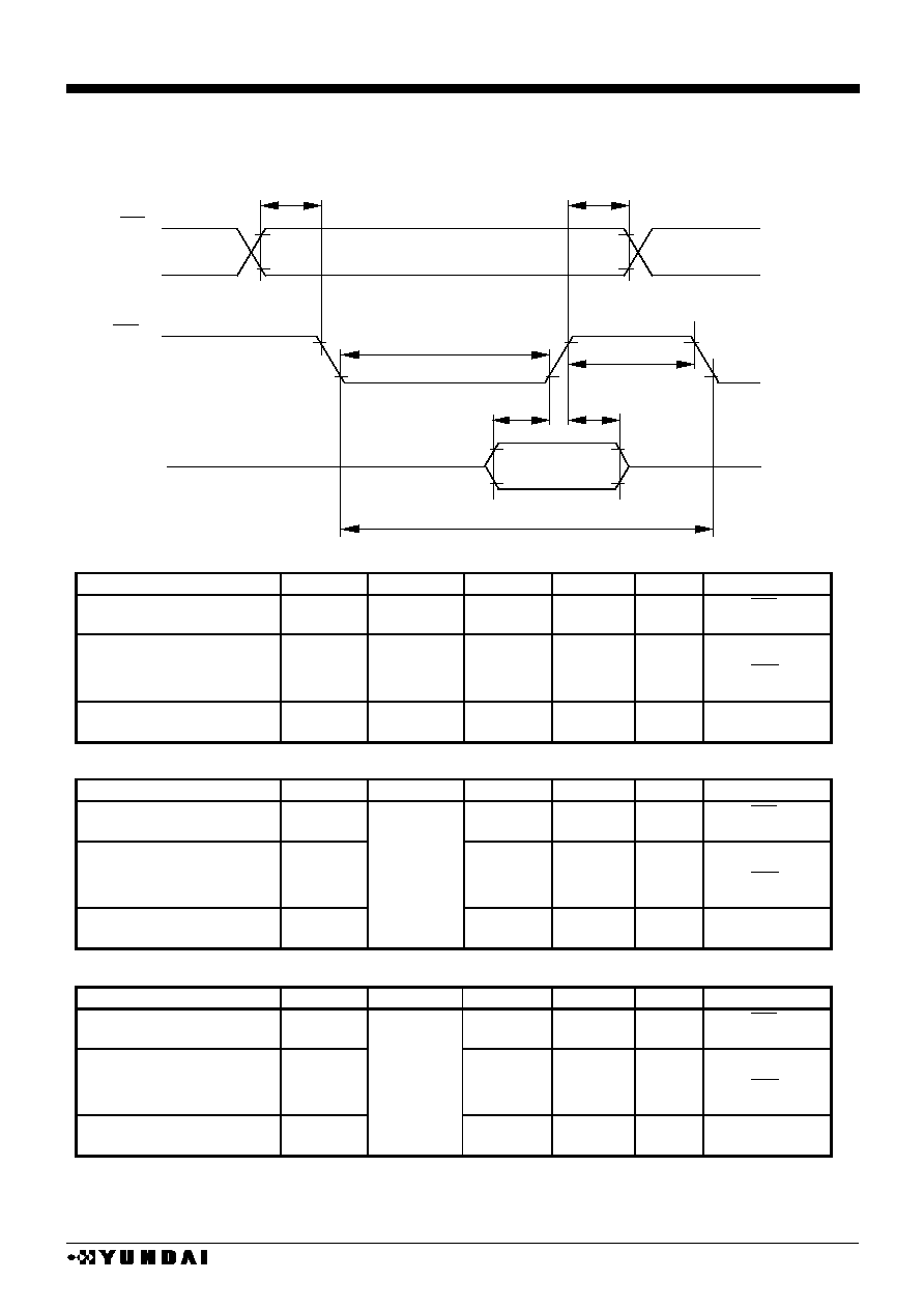
HM17CM256
- 97 -
s
AC CHARACTERISTICS
�
SYSTEM BUS READ / WRITE TIMING (80 series CPU interface)
(write timing)
(V
DD
=2.7
3.3V, Ta=-30
+85
�
C)
ITEM
SYMBOL
CONDITION
MIN.
MAX.
UNIT
PORT
Address hold timing
Address setup timing
t
AH8
t
AS8
TBD
TBD
ns
ns
CS
RS
System cycle timing
Write "L" pulse width
Write "H" pulse width
t
CYC8
t
WRLW8
t
WRHW8
TBD
TBD
TBD
ns
ns
ns
WR
Data setup timing
Data hold timing
t
DS8
t
DH8
TBD
TBD
ns
ns
D
0
D
15
(V
DD
=2.4
2.7V, Ta=-30
+85
�
C)
ITEM
SYMBOL
CONDITION
MIN.
MAX.
UNIT
PORT
Address hold timing
Address setup timing
t
AH8
t
AS8
TBD
TBD
ns
ns
CS
RS
System cycle timing
Write "L" pulse width
Write "H" pulse width
t
CYC8
t
WRLW8
t
WRHW8
TBD
TBD
TBD
ns
ns
ns
WR
Data setup timing
Data hold timing
t
DS8
t
DH8
TBD
TBD
ns
ns
D
0
D
15
(V
DD
=1.7
2.4V, Ta=-30
+85
�
C)
ITEM
SYMBOL
CONDITION
MIN.
MAX.
UNIT
PORT
Address hold timing
Address setup timing
t
AH8
t
AS8
TBD
TBD
ns
ns
CS
RS
System cycle timing
Write "L" pulse width
Write "H" pulse width
t
CYC8
t
WRLW8
t
WRHW8
TBD
TBD
TBD
ns
ns
ns
WR
Data setup timing
Data hold timing
t
DS8
t
DH8
TBD
TBD
ns
ns
D
0
D
15
notice) All timing reference is 20% and 80% of V
DD
and 80%.
t
CYC8
t
AS8
CS
WR
RS
D
0
D
15
t
AH8
t
WRLW8
t
WRHW8
t
DS8
t
DH8

HM17CM256
- 98 -
�
read timing
�
(V
DD
=2.7
3.3V, Ta=-30
+85
�
C)
ITEM
SYMBOL
CONDITION
MIN.
MAX.
UNIT
PORT
Address hold timing
Address setup timing
t
AH8
t
AS8
TBD
TBD
ns
ns
CS
RS
System cycle timing
Write "L" pulse width
Write "H" pulse width
t
CYC8
t
WRLR8
t
WRHR8
TBD
TBD
TBD
ns
ns
ns
RD
Data setup timing
Data hold timing
t
DS8
t
DH8
TBD
TBD
ns
ns
D
0
D
15
(V
DD
=2.4
2.7V, Ta=-30
+85
�
C)
ITEM
SYMBOL
CONDITION
MIN.
MAX.
UNIT
PORT
Address hold timing
Address setup timing
t
AH8
t
AS8
TBD
TBD
ns
ns
CS
RS
System cycle timing
Write "L" pulse width
Write "H" pulse width
t
CYC8
t
WRLR8
t
WRHR8
TBD
TBD
TBD
ns
ns
ns
RD
Data setup timing
Data hold timing
t
DS8
t
DH8
TBD
TBD
ns
ns
D
0
D
15
(V
DD
=1.7
2.4V, Ta=-30
+85
�
C)
ITEM
SYMBOL
CONDITION
MIN.
MAX.
UNIT
PORT
Address hold timing
Address setup timing
t
AH8
t
AS8
TBD
TBD
ns
ns
CS
RS
System cycle timing
Write "L" pulse width
Write "H" pulse width
t
CYC8
t
WRLR8
t
WRHR8
TBD
TBD
TBD
ns
ns
ns
RD
Data setup timing
Data hold timing
t
DS8
t
DH8
TBD
TBD
ns
ns
D
0
D
15
notice) All timing reference is 20% and 80% of V
DD
and 80%.
t
AS8
CS
RS
D
0
D
15
t
RDD8
t
RDH8
t
CYC8
RD
t
WRLR8
t
WRHR8
t
AH8
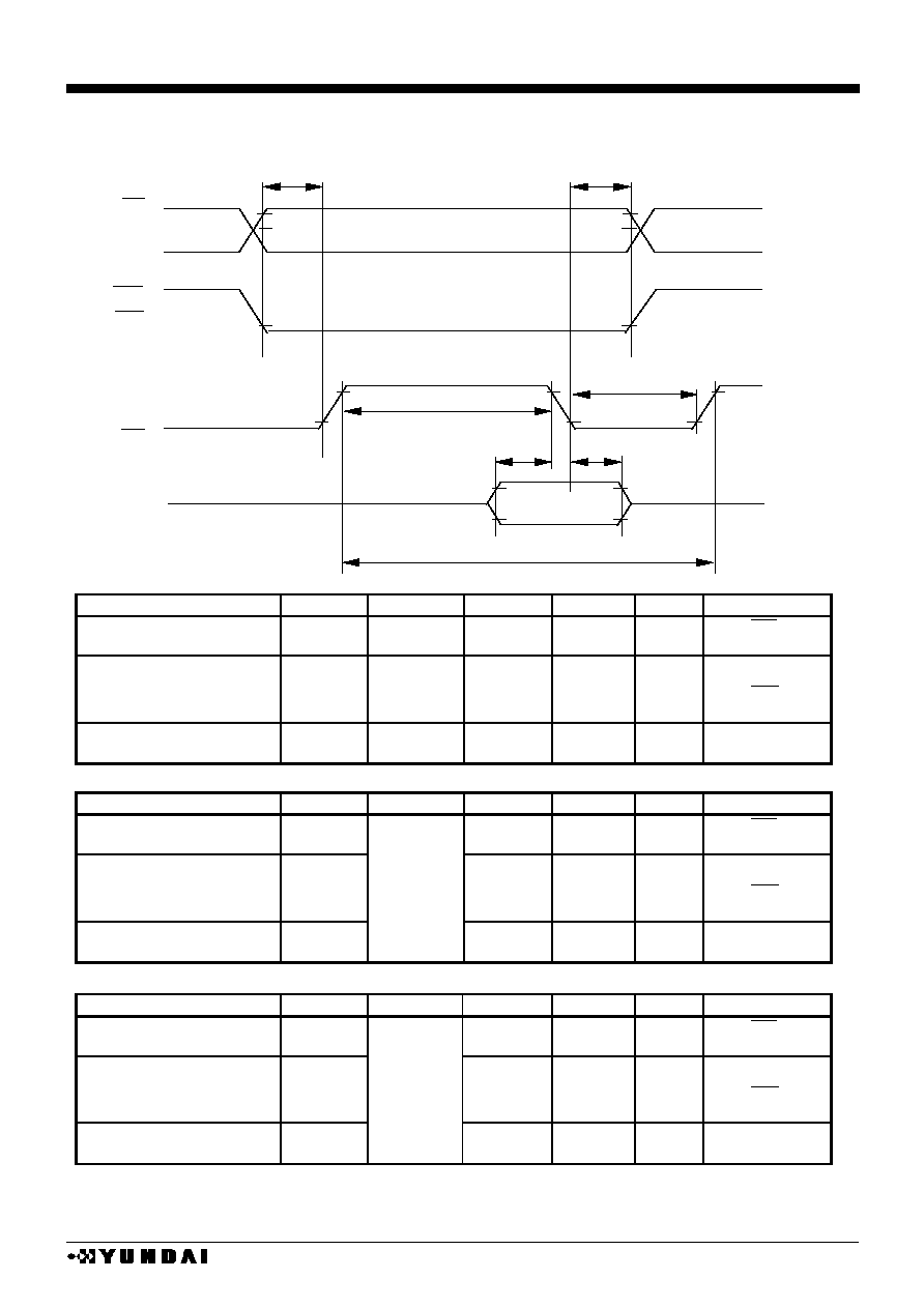
HM17CM256
- 99 -
�
SYSTEM BUS READ / WRITE TIMING (68 series CPU interface)
(write timing
�
(V
DD
=2.7
3.3V, Ta=-30
+85
�
C)
ITEM
SYMBOL
CONDITION
MIN.
MAX.
UNIT
PORT
Address hold timing
Address setup timing
t
AH6
t
AS6
TBD
TBD
ns
ns
CS
RS
System cycle timing
Enable "L" pulse width
Enable "H" pulse width
t
CYC6
t
ELW6
t
EHW6
TBD
TBD
TBD
ns
ns
ns
E
Data setup timing
Data hold timing
t
DS6
t
DH6
TBD
TBD
ns
ns
D
0
D
15
(V
DD
=2.4
2.7V, Ta=-30
+85
�
C)
ITEM
SYMBOL
CONDITION
MIN.
MAX.
UNIT
PORT
Address hold timing
Address setup timing
t
AH6
t
AS6
TBD
TBD
ns
ns
CS
RS
System cycle timing
Enable "L" pulse width
Enable "H" pulse width
t
CYC6
t
ELW6
t
EHW8
TBD
TBD
TBD
ns
ns
ns
E
Data setup timing
Data hold timing
t
DS6
t
DH6
TBD
TBD
ns
ns
D
0
D
15
(V
DD
=1.7
2.4V, Ta=-30
+85
�
C)
ITEM
SYMBOL
CONDITION
MIN.
MAX.
UNIT
PORT
Address hold timing
Address setup timing
t
AH6
t
AS6
TBD
TBD
ns
ns
CS
RS
System cycle timing
Enable "L" pulse width
Enable "H" pulse width
t
CYC6
t
ELW6
t
EHW6
TBD
TBD
TBD
ns
ns
ns
E
Data setup timing
Data hold timing
t
DS6
t
DH6
TBD
TBD
ns
ns
D
0
D
15
notice) All timing reference is 20% and 80% of V
DD
and 80%.
t
AS6
CS
RS
t
AH6
R/W
(WR)
D
0
D
15
t
EHW6
t
ELW6
t
DS6
t
DH6
t
CYC6
E
(RD)

HM17CM256
- 100 -
(read timing)
(V
DD
=2.7
3.3V, Ta=-30
+85
�
C)
ITEM
SYMBOL
CONDITION
MIN.
MAX.
UNIT
PORT
Address hold timing
Address setup timing
t
AH6
t
AS6
TBD
TBD
ns
ns
CS
RS
System cycle timing
Enable "L" pulse width
Enable "H" pulse width
t
CYC6
t
ELR6
t
EHR6
TBD
TBD
TBD
ns
ns
ns
E
Data setup timing
Data hold timing
t
DS6
t
DH6
TBD
TBD
ns
ns
D
0
D
15
(V
DD
=2.4
2.7V, Ta=-30
+85
�
C)
ITEM
SYMBOL
CONDITION
MIN.
MAX.
UNIT
PORT
Address hold timing
Address setup timing
t
AH6
t
AS6
TBD
TBD
ns
ns
CS
RS
System cycle timing
Enable "L" pulse width
Enable "H" pulse width
t
CYC6
t
ELR6
t
EHR8
TBD
TBD
TBD
ns
ns
ns
E
Data setup timing
Data hold timing
t
DS6
t
DH6
TBD
TBD
ns
ns
D
0
D
15
(V
DD
=1.7
2.4V, Ta=-30
+85
�
C)
ITEM
SYMBOL
CONDITION
MIN.
MAX.
UNIT
PORT
Address hold timing
Address setup timing
t
AH6
t
AS6
TBD
TBD
ns
ns
CS
RS
System cycle timing
Enable "L" pulse width
Enable "H" pulse width
t
CYC6
t
ELR6
t
EHR6
TBD
TBD
TBD
ns
ns
ns
E
Data setup timing
Data hold timing
t
DS6
t
DH6
TBD
TBD
ns
ns
D
0
D
15
notice) All timing reference is 20% and 80% of V
DD
and 80%.
t
AS6
CS
RS
t
AH6
R/W
(WR)
D
0
D
15
t
EHR6
t
ELR6
t
RDD6
t
RDH6
t
CYC6
E
(RD)
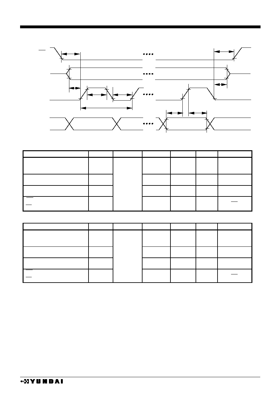
HM17CM256
- 101
-
�
SERIAL INTERFACE TIMING
(V
DD
=2.7
3.3V, Ta=-30
+85
�
C)
ITEM
SYMBOL
CONDITION
MIN.
MAX.
UNIT
PORT
Serial clock cycle
SCL "H" pulse width
SCL "L" pulse width
t
CYCS
t
SHW
t
SLW
TBD
TBD
TBD
ns
ns
ns
SCL
Address setup timing
Address hold timing
t
ASS
t
AHS
TBD
TBD
ns
ns
RS
Data setup timing
Data hold timing
t
DSS
t
DHS
TBD
TBD
ns
ns
SDA
CS � SCL timing
CS hold timing
t
CSS
t
CSH
TBD
TBD
ns
ns
(V
DD
=2.4
2.7V, Ta=-30
+85
�
C)
ITEM
SYMBOL
CONDITION
MIN.
MAX.
UNIT
PORT
Serial clock cycle
SCL "H" pulse width
SCL "L" pulse width
t
CYCS
t
SHW
t
SLW
TBD
TBD
TBD
ns
ns
ns
SCL
Address setup timing
Address hold timing
t
ASS
t
AHS
TBD
TBD
ns
ns
RS
Data setup timing
Data hold timing
t
DSS
t
DHS
TBD
TBD
ns
ns
SDA
CS � SCL timing
CS hold timing
t
CSS
t
CSH
TBD
TBD
ns
ns
notice) All timing reference is 20% and 80% of V
DD
and 80%.
CS
t
CSS
CS
RS
t
CSH
SDA
t
SLW
t
SHW
t
DSS
t
DHS
t
CYCS
SCL
t
AHS
t
ASS
CS

HM17CM256
- 102 -
(V
DD
=1.7
2.4V, Ta=-30
+85
�
C)
ITEM
SYMBOL
CONDITION
MIN.
MAX.
UNIT
PORT
Serial clock cycle
SCL "H" pulse width
SCL "L" pulse width
t
CYCS
t
SHW
t
SLW
TBD
TBD
TBD
ns
ns
ns
SCL
Address setup timing
Address hold timing
t
ASS
t
AHS
TBD
TBD
ns
ns
RS
Data setup timing
Data hold timing
t
DSS
t
DHS
TBD
TBD
ns
ns
SDA
CS � SCL timing
CS hold timing
t
CSS
t
CSH
TBD
TBD
ns
ns
notice) All timing reference is 20% and 80% of V
DD
and 80%.
CS

HM17CM256
- 103
-
�
DISPLAY CONTROL TIMING
INPUT TIMING ( slave mode )
(V
DD
=2.4
3.3V, Ta=-30
+85
�
C)
ITEM
SYMBOL
CONDITION
MIN.
MAX.
UNIT
PORT
CL "H" pulse width
CL "L" pulse width
t
CLHW
t
CLLW
80
80
�
s
�
s
CL
FLM delay time
t
DFLM
-1.0
1.0
�
s
FLM
FR delay time
t
FR
-1.0
1.0
�
s
FR
INPUT TIMING ( slave mode )
(V
DD
=1.7
2.4V, Ta=-30
+85
�
C)
ITEM
SYMBOL
CONDITION
MIN.
MAX.
UNIT
PORT
CL "H" pulse width
CL "L" pulse width
t
CLHW
t
CLLW
80
80
�
s
�
s
CL
FLM delay time
t
DFLM
-1.0
1.0
�
s
FLM
FR delay time
t
FR
-1.0
1.0
�
s
CL
OUTPUT TIMING ( master mode )
(V
DD
=2.4
3.3V, Ta=-30
+85
�
C)
ITEM
SYMBOL
CONDITION
MIN.
MAX.
UNIT
PORT
FLM delay time
t
DFLM
CL=15pF
10
500
ns
FLM
FR delay time
t
FR
10
500
ns
FR
OUTPUT TIMING ( master mode )
(V
DD
=1.7
2.4V, Ta=-30
+85
�
C)
ITEM
SYMBOL
CONDITION
MIN.
MAX.
UNIT
PORT
FLM delay time
t
DFLM
CL=15pF
10
1000
ns
FLM
FR delay time
t
FR
10
1000
ns
FR
notice) All timing reference is 20% and 80% of V
DD
and 80%.
CL
t
CLLW
FR
t
DFLM
t
DM
FLM
t
DFLM
t
CLHW
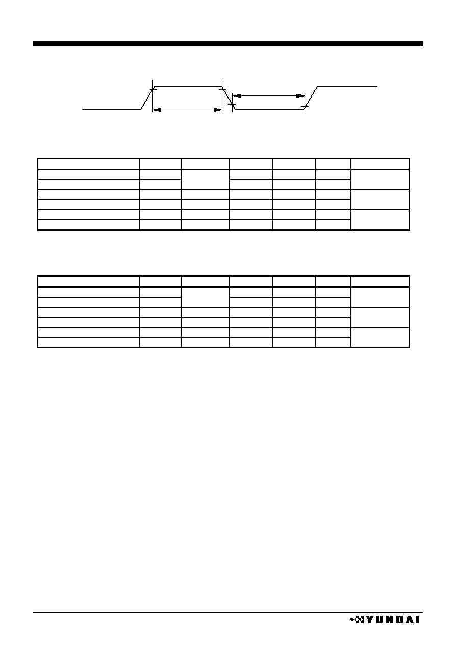
HM17CM256
- 104 -
�
SOURCE CLOCK INPUT TIMING
(V
DD
=2.4
3.3V, Ta=-30
+85
�
C)
ITEM
SYMBOL
CONDITION
MIN.
MAX.
UNIT
PORT
OSC
1
"H" pulse width (1)
t
CKHW1
TBD
TBD
�
s
OSC
1
OSC
1
"L" pulse width (1)
t
CKLW1
TBD
TBD
�
s
1
OSC
1
"H" pulse width (2)
t
CKHW2
TBD
TBD
�
s
OSC
1
OSC
1
"L" pulse width (2)
t
CKLW2
TBD
TBD
�
s
2
OSC
1
"H" pulse width (3)
t
CKHW3
TBD
TBD
�
s
OSC
1
OSC
1
"L" pulse width (3)
t
CKLW3
TBD
TBD
�
s
3
(V
DD
=1.7
2.4V, Ta=-30
+85
�
C)
ITEM
SYMBOL
CONDITION
MIN.
MAX.
UNIT
PORT
OSC
1
"H" pulse width (1)
t
CKHW1
TBD
TBD
�
s
OSC
1
OSC
1
"L" pulse width (1)
t
CKLW1
TBD
TBD
�
s
1
OSC
1
"H" pulse width (2)
t
CKHW2
TBD
TBD
�
s
OSC
1
OSC
1
"L" pulse width (2)
t
CKLW2
TBD
TBD
�
s
2
OSC
1
"H" pulse width (3)
t
CKHW3
TBD
TBD
�
s
OSC
1
OSC
1
"L" pulse width (3)
t
CKLW3
TBD
TBD
�
s
3
notice) All timing reference is 20% and 80% of V
DD
and 80%.
1 applicable under gradation display , MON="0", PWM="0"
2 applicable under fixed gradation display , MON="0",PWM="1"
3 applicable under BW display , MON="1"
OSC
1
t
CKLW
t
CKHW
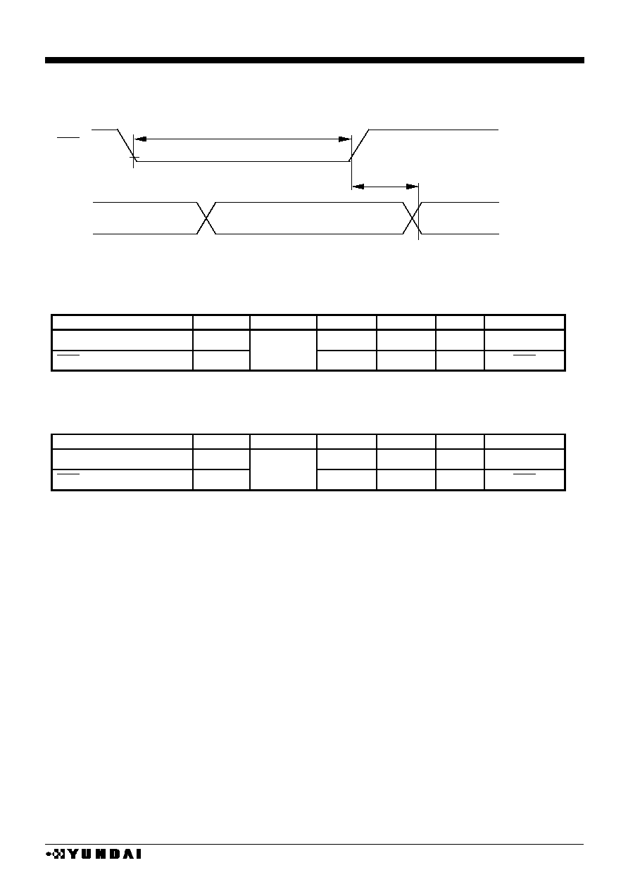
HM17CM256
- 105
-
�
RESET INPUT TIMING
(V
DD
=2.4
3.3V, Ta=-30
+85
�
C)
ITEM
SYMBOL
CONDITION
MIN.
MAX.
UNIT
PORT
Reset time
t
R
1.0
�
s
RES "L" pulse width
t
RW
10.0
�
s
RES
(V
DD
=1.7
2.4V, Ta=-30
+85
�
C)
ITEM
SYMBOL
CONDITION
MIN.
MAX.
UNIT
PORT
Reset time
t
R
1.5
�
s
RES "L" pulse width
t
RW
10.0
�
s
RES
notice) All timing reference is 20% and 80% of V
DD
and 80%.
Internal status
Reset completion
resetting
t
RW
RES
t
R

HM17CM256
- 106 -
s
APPLICATION EXAMPLE
�
�
reference
�
�
(1) connection with CPU
a) 80 series CPU interface
b) 68 series CPU interface
c) CPU connection with serial interface
A
0
V
CC
A
1
~ A
7
PORT
1
PORT
2
RES
GND
7
Decoder
RS
CS
SDA
SCL
RES
V
DD
V
SS
Reset input
1.7V ~ 3.3V
(CPU)
A
0
V
CC
A
1
~ A
7
IORQ
D
0
~ D
7
RD
WR
RES
GND
7
Decoder
RS
CS
D
0
~ D
7
RD
WR
RES
V
DD
V
SS
8
Reset input
1.7V ~ 3.3V
(
80
s
e
r
i
e
s
C
P
U
)
A
0
V
CC
A
1
~ A
15
VMA
D
0
~ D
7
E
R/W
RES
GND
15 Decoder
RS
CS
D
0
~ D
7
RD(E)
WR(R/W)
RES
V
DD
V
SS
8
Reset input
1.7V ~ 3.3V
(
68
s
e
r
i
e
s
C
P
U
)
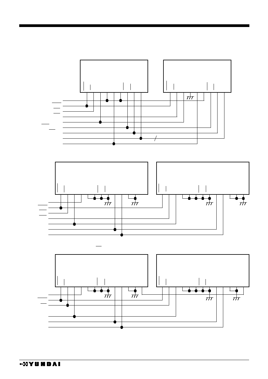
HM17CM256
- 107
-
(2) MULTI CHIP INTERFACE
a) connection example of input interface
(parallel interface)
(4-line type serial interface)
(4-line type serial interface, CS
1
common)
W
R
D
0
~
D
7
RD
SE
L68
P
/
S
M
/
S
R
S
C
S
R
ES
(Slave)
W
R
D
0
~
D
7
RD
SE
L68
P
/
S
M
/
S
R
S
C
S
R
ES
(Master)
V
DD
RES
CS
1
CS
2
RS
WR(R/W)
RD(E)
D
0
~ D
7
SEL68
8
V
DD
RES
CS
1
CS
2
RS
SDA
SCL
SP
O
L
E
X
C
S
S
M
O
D
E
S
D
A
S
C
L
RD
W
R
P
/
S
SE
L68
(Master)
M
/
S
R
S
C
S
R
ES
SP
O
L
E
X
C
S
S
M
O
D
E
S
D
A
S
C
L
RD
W
R
P
/
S
SE
L68
(Slave)
M
/
S
R
S
C
S
R
ES
V
DD
RES
CS
RS
SDA
SCL
SP
O
L
E
X
C
S
S
M
O
D
E
S
D
A
S
C
L
RD
W
R
P
/
S
SE
L68
(Master)
M
/
S
R
S
C
S
R
ES
SP
O
L
E
X
C
S
S
M
O
D
E
S
D
A
S
C
L
RD
W
R
P
/
S
SE
L68
(Slave)
M
/
S
R
S
C
S
R
ES

HM17CM256
- 108 -
(3-line type serial interface)
(3-line type serial interface, CS
1
common)
V
DD
RES
CS
1
CS
2
SDA
SCL
SP
O
L
E
X
C
S
S
M
O
D
E
S
D
A
S
C
L
RD
W
R
P
/
S
SE
L68
(Master)
M
/
S
R
S
C
S
R
ES
SP
O
L
E
X
C
S
S
M
O
D
E
S
D
A
S
C
L
RD
W
R
P
/
S
SE
L68
(Slave)
M
/
S
R
S
C
S
R
ES
V
DD
RES
CS
SDA
SCL
SP
O
L
E
X
C
S
S
M
O
D
E
S
D
A
S
C
L
RD
W
R
P
/
S
SE
L68
(Master)
M
/
S
R
S
C
S
R
ES
SP
O
L
E
X
C
S
S
M
O
D
E
S
D
A
S
C
L
RD
W
R
P
/
S
SE
L68
(Slave)
M
/
S
R
S
C
S
R
ES

HM17CM256
- 109
-
a) connection example of power supply
Be cautious of using as following description when LCD panel is connected with master/slave structure.
1) Display timing is controlled by master chip. The CL, FLM, FR, CLK signals are stopped when master
chip is display OFF. When you are going to OFF the display, please OFF the display of slave chip first
before master chip display is OFF.
2) Boosting circuit and voltage converting circuit is OFF after execution HALT command at master chip,
then LCD driving output is V
SS
level and so display is OFF. And Voltage common is stopped. Because
the voltage common of slave chip is stopped, please run slave chip display OFF first and then run master
chip HALT command.
3) The electric volume setting is valid at master chip only(at upper structure).
4) To protect that V
OUT
is being floated, please connect V
OUT
with V
LCD
voltage level.
5) Please use under condition that OSC
1
and OSC
2
port of slave chip is OFF.
V
DD
V
EE
V
BA
V
REF
C
1
+
C
1
-
CA
1
C
2
+
C
2
-
CA
1
C
3
+
C
3
-
CA
1
C
5
+
C
5
-
CA
1
V
LCD
V
1
V
2
V
3
V
4
CA
2
CA
2
CA
2
CA
2
CA
2
V
OUT
V
REG
CA
1
V
SS
CA
3
V
SS
CLK
CL
FLM
FR
V
LCD
V
1
V
2
V
3
V
4
V
DD
V
DD
V
DD
V
EE
V
BA
V
REF
V
LCD
V
1
V
2
V
3
V
4
V
OUT
CLK
CL
FLM
FR
(
M
a
s
t
e
r)
(
S
l
a
v
e
)
V
REG
C
4
+
C
4
-
CA
1
C
6
+
C
6
-
CA
1
C
1
+
C
1
-
C
2
+
C
2
-
C
3
+
C
3
-
C
5
+
C
5
-
C
4
+
C
4
-
C
6
+
C
6
-
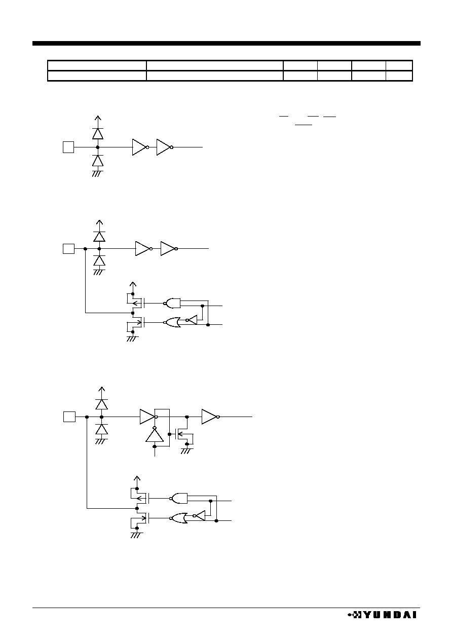
HM17CM256
- 110 -
�
Typical characteristic
ITEM
CONDITION
MIN
TYP
MAX UNIT
Basic delay time of gate
Ta=+25
�
C, V
SS
=0V, V
DD
=3.0V
10
ns
�
IN/OUTPUT CIRCUIT STRUCTURE
(a) input circuit 1
port : CS, RS, RD, WR, SEL68, M/S
P/S, RES
(b-1) in/out circuit 1
port : FLM, LP, FR, CLK
(b-2) in/out circuit 2
port : D
0
~D
15
V
DD
I
V
SS
(0V)
Input signal
I/O
V
DD
V
SS
(0V)
Input signal
V
DD
V
SS
(0V)
Output control signal
Output signal
I/O
V
DD
V
SS
(0V)
Input signal
V
DD
V
SS
(0V)
Output control signal
Output signal
V
SS
(0V)
Input control signal

HM17CM256
- 111
-
(c) LCD driver output circuit
Port : SEGA
0
~SEGA
127
SEGB
0
~SEGB
127
SEGC
0
~SEGC
127
COM
0
~COM
79
COMI
0
, COMI
1
SEGSA
0
, SEGSR
1
SEGSB
0
, SEGSB
1
SEGSC
0
, SEGSC
1
<precautions>
The details of this specification was written
sincerely, but it is not a letter of guarantee of
legal. Especially, the application circuit is just
for reference.
This specification do not guarantee that we did
not use others patent or intellectural property.
output control
signal 1
output control
signal 3
output control
signal 2
output control
signal 4
O
V
LCD
V
SS
(0V)
V
1
/V
2
V
SS
(0V)
V
LCD
V
SS
(0V)
V
3
/V
4
V
LCD