
8-BIT SINGLE-CHIP MICROCONTROLLERS
HMS77C2000
HMS77C2001
User's Manual
(Ver. 1.1)

HMS77C2000/2001
2
Nov. 2002 Ver 1.1
Version 1.1
Published by
MCU Application Team
2002 Hynix Semiconductor All right reserved.
Additional information of this manual may be served by Hynix Semiconductor offices in Korea or Distributors and Representatives listed
at address directory.
Hynix Semiconductor reserves the right to make changes to any information here in at any time without notice.
The information, diagrams and other data in this manual are correct and reliable; however, Hynix Semiconductor is in no way responsible
for any violations of patents or other rights of the third party generated by the use of this manual.
Revision History
Ver 1.1 (this manual, NOV. 2002)
Add I
OL
-V
OL
, I
OH
-V
OH
and V
PP
rising & falling time graphs in the electrical characteristics.
Correct mistakes in the paragraph.

HMS77C2000/2001
Oct. 2002 Ver 1.1
1
Table of Contents
1. GENERAL DESCRIPTION ...................2
Application .................................................. 2
One-Time-Programmable (OTP) Devices .. 2
2. BLOCK DIAGRAM ................................3
3. PIN ASSIGNMENT ...............................3
4. PACKAGE DIAGRAM ...........................4
5. PIN FUNCTION .....................................5
6. PORT STRUCTURES ...........................6
7. ELECTRICAL CHARACTERISTICS .....8
Absolute Maximum Ratings ........................ 8
Recommended Operating Conditions ......... 8
DC Characteristics (1) ................................ 9
DC Electrical Characteristics (2) ............... 10
AC Electrical Characteristics (1) ............... 11
AC Electrical Characteristics (2) ............... 12
Typical Characteristics .............................. 13
8. ARCHITECTURAL OVERVIEW ..........16
CPU Architecture ...................................... 16
Clocking Scheme/Instruction Cycle .......... 17
Instruction Flow/Pipelining ........................ 17
9. MEMORY ORGANIZATION ................18
Program Memory Organization ................. 18
Data Memory Organization ....................... 18
STATUS Register ..................................... 21
OPTION Register ...................................... 21
OSCCAL Register ..................................... 23
Program Counter ...................................... 23
Stack ......................................................... 24
Indirect Data Addressing; INDF and FSR
Registers ................................................... 25
10. I/O PORT ..........................................26
UPIO ......................................................... 26
TRIS Register ............................................26
I/O Interfacing ............................................26
I/O Programming Considerations ..............27
11. TIMER0 MODULE AND TMR0
REGISTER ..........................................29
Using Timer0 with an External Clock ........30
Prescaler ...................................................31
12. SPECIAL FEATURES OF THE CPU 33
Configuration Bits ......................................33
Oscillator Configurations ...........................34
Reset .........................................................35
Power-On Reset (POR) .............................37
Internal Reset Timer (IRT) .........................39
Watchdog Timer (WDT) ............................39
Time-Out Sequence, Power Down, and
Wake-up from SLEEP Status Bits (TO/PD/UPWUF)
40
Reset on Brown-Out ..................................41
Power-Down Mode (SLEEP) .....................41
Program Verification/Code Protection .......42
ID Locations ..............................................42
Power Fail Detection Processor ................42
In-Circuit Serial Programming ...................43
13. IN-CIRCUIT SERIAL PROGRAM-
MING(ICSP) SPECIFICATIONS .........45
Programming The HMS77C200x ..............45
Program Mode Entry .................................45
Configuration Word ...................................49
Code Protection .........................................50
Program/Verify Mode Electrical Characteristics
52

HMS77C2000/2001
Nov. 2002 Ver 1.1
1
HMS77C2000/2001
8 PIN, 8-BIT CMOS SINGLE-CHIP MICROCONTROLLER
High-Performance RISC CPU:
- Only 33 single word instructions to learn
- All instructions are single cycle (1 us) except for
program branches which are two-cycle
- Operating speed: DC - 4 MHz clock input
DC - 1 us instruction cycle
- 12-bit
wide
instructions and 8-bit wide data path
- Seven special function hardware registers
- Two-level deep hardware stack
- Direct, indirect and relative addressing modes
for data and instructions
- Internal 4 MHz RC oscillator with programmable
calibration
- In-circuit
serial
programming
Peripheral Features:
- 8-bit real time clock/counter (TMR0) with 8-bit
programmable prescaler
- Power-On Reset (POR)
- Internal Reset Timer (IRT)
- Watchdog Timer (WDT) with its own on-chip RC
oscillator for reliable operation
- Programmable
code-protection
- Noise immunity circuit: Power fail detector
- Power
saving SLEEP mode
- Wake-up from SLEEP on pin change
- Internal weak pull-ups on I/O pins
- Internal pull-up on RESET pin
- Selectable
oscillator
options:
IRC: Internal 4 MHz RC oscillator
ERC: External low-cost RC oscillator
(200KHz ~ 4MHz)
XT: Standard crystal/resonator
(455KHz ~ 4MHz)
LF: Power saving, low frequency crystal
(32KHz ~ 200KHz)
CMOS Technology:
- Low power, high speed CMOS EPROM
technology
- Wide operating voltage range
- Wide
temperature
range:
Industrial: -40
�
C to +85
�
C
- Low power consumption
< 2 mA typical @5V, 4 MHz
30 uA typical @3V, 32 kHz
0.25 uA typical standby current
@3V, WDT disable
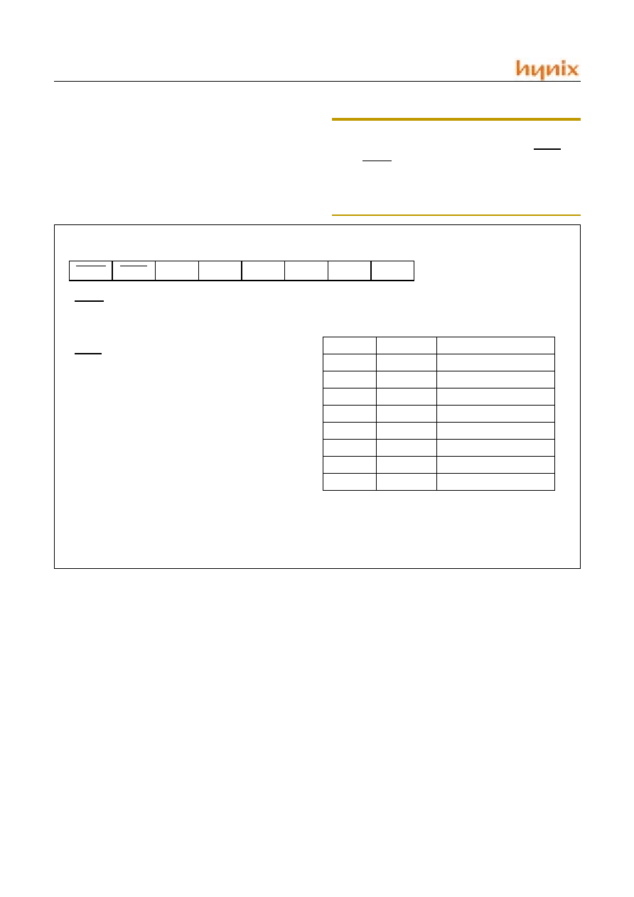
Device name
EPROM(12bit)
RAM
I/O, I
Timer
Voltage Range
Package
HMS77C2000
512 words
25 bytes
5, 1
1
2.5 ~ 5.5V
8 PDIP, SOP
HMS77C2001
1024 words
41 bytes

HMS77C2000/2001
2
Nov. 2002 Ver 1.1
1. GENERAL DESCRIPTION
The HMS77C2000 and HMS77C2001 are an advanced
CMOS 8-bit microcontrollers with 0.5K/1K words
(12bits) of EPROM. They employ a RISC architecture
with only 33 single word/single cycle instructions. All in-
structions are single cycle (1us) except for program
branches which take two cycles. The HMS77C2000 and
HMS77C2001 deliver performance an order of magnitude
higher than their competitors in the same price category.
The HMS77C2000 and HMS77C2001 products are
equipped with special features that reduce system cost and
power requirements. The Power-on reset (POR) and inter-
nal reset timer (IRT) remove the need for external reset cir-
cuitry. There are four oscillator configurations to choose
from IRC (internal RC) oscillator mode to LF (Low Fre-
quency) oscillator mode. Power saving SLEEP mode,
watchdog timer and code protection features also improve
system cost, power and reliability. The HMS77C2000 and
HMS77C2001 are available in the cost-effective one-time-
programmable (OTP) versions which are suitable for pro-
duction in any volume. The customer can take full advan-
tage of Hynix Semiconductor's price leadership in OTP
microcontrollers while benefiting from the OTP's flexibil-
ity. Also the HMS77C2000 and HMS77C2001 have an on-
chip power fail detection circuitry to immunize against
power noise. The power fail detection processor may reset
MCU to protect the device from malfunction due to power
noise.
1.1 APPLICATION
The HMS77C2000 and HMS77C2001 fit perfectly in ap-
plications ranging from personal care appliances and secu-
rity systems to low-power remote transmitters/receivers.
The EPROM technology makes customizing application
programs (transmitter codes, appliance settings, receiver
frequencies, etc.) extremely fast and convenient. The small
footprint packages or surface mounting make these micro-
controllers perfect for applications with space limitations.
Low-cost, low-power, high performance, ease of use and I/
O flexibility make the HMS77C2000 and HMS77C2001
very versatile even in areas where no microcontroller use
has been considered before (e.g., timer functions, copro-
cessor applications).
1.2 ONE-TIME-PROGRAMMABLE (OTP)
DEVICES
The availability of OTP devices is especially useful for
customers who need the flexibility for frequent code up-
dates or small volume applications.
The OTP devices, packaged in plastic packages permit the
user to program them once. In addition to the program
memory, the configuration bits must also be programmed.
HMS77C2000/2001
Nov. 2002 Ver 1.1
3
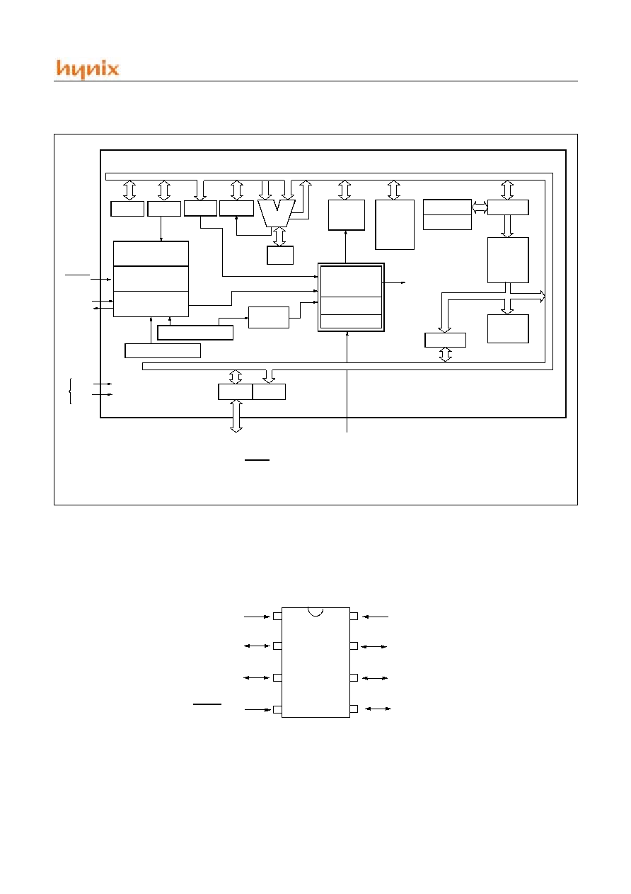
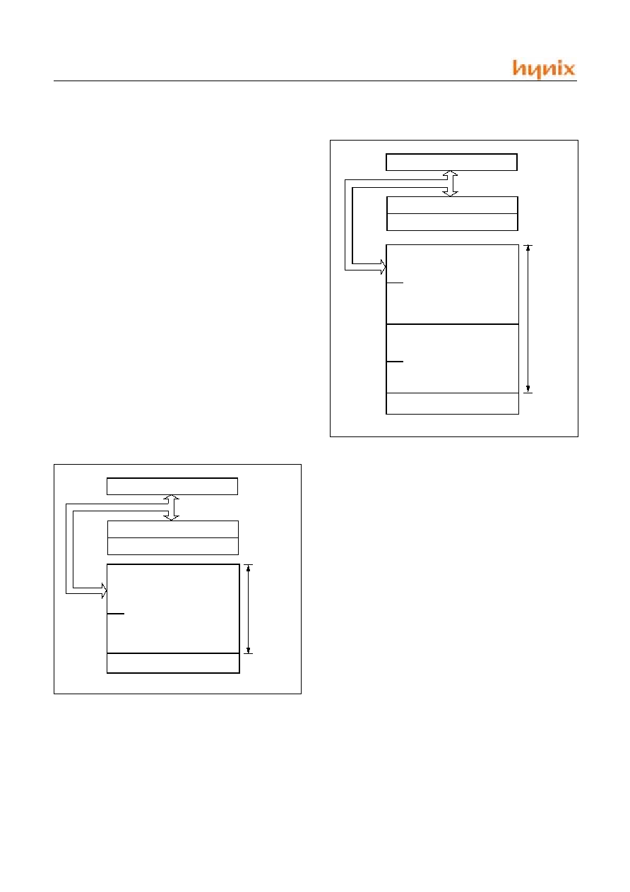
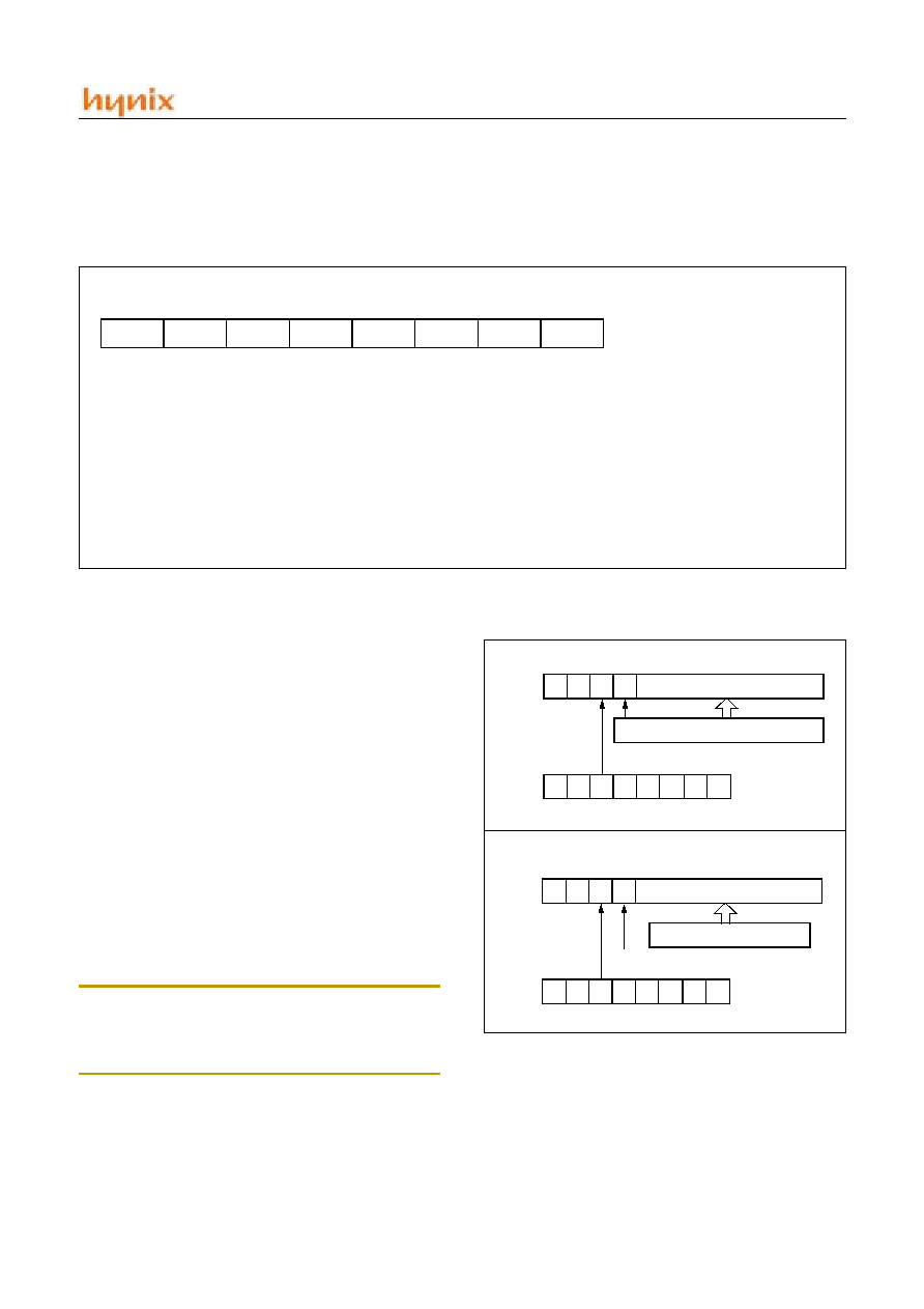
2. BLOCK DIAGRAM
3. PIN ASSIGNMENT
FIGURE 2-1 HMS77C2000/20001 BLOCK DIAGRAM
W
STACK 1
Data
Memory
8-bit
Counter
Timer/
Program
Memory
PC
WDT/
Prescaler
Watch-dog
Timer
Instruction
UPIO
STATUS
System controller
Clock Generator
RESET
Xin
Xout
UP0
UP1
UP2/EC0
UP3/RESET/V
PP
V
DD
V
SS
Power
Supply
Decoder
EC0
WDT time out
ALU
STACK 2
TMR0
Power Fail Detector
Timing Control
Configuration Word
TRIS
FSR
UP4/X
OUT
UP5/X
IN
Internal Reset
Timer
Powe-on Reset
Internal RC OSC
ICSP
OSCCAL OPTION
V
SS
UP0
UP1
UP2/EC0
V
DD
UP5/X
IN
UP4/X
OUT
UP3/RESET/V
PP
8 PDIP or SOP
1
2
3
4
8
7
6
5
HMS77C2000
HMS77C2001
HMS77C2000/2001
4
Nov. 2002 Ver 1.1
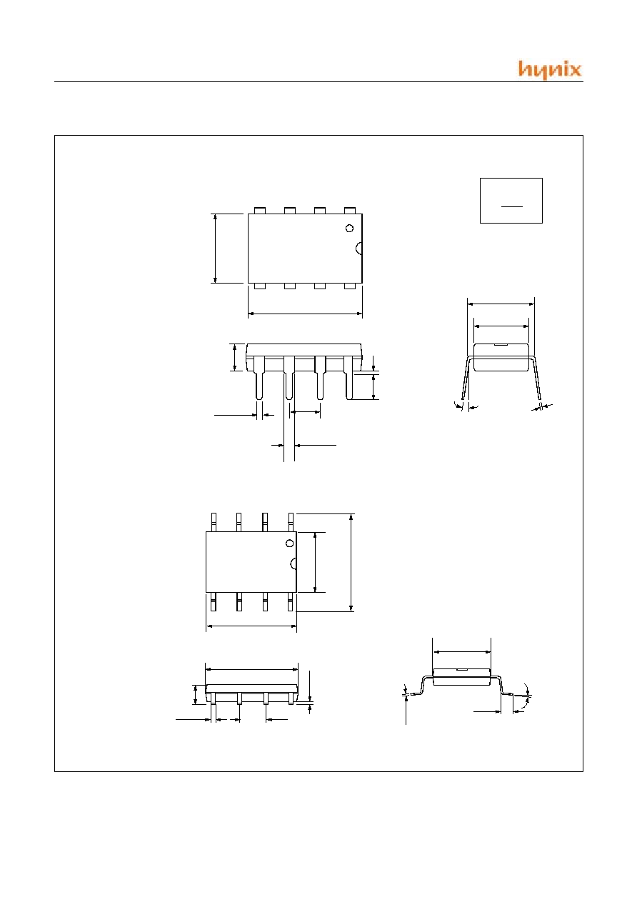
4. PACKAGE DIAGRAM
0.387
0.015
0.050
TYP 0.100
TYP 0.300
0.260
0.014
3� ~ 15�
MA
X 0.1
8
0
MIN 0.0
2
0
0.1
2
0
0
.
152
0.23
0
0.195
0.0688
0.0138
TYP 0.050
0
.
004
0.007
5
0� ~ 8�
0.016
8 PDIP (300MIL)
8 SOP (150MIL)
unit: inch
MAX
MIN
0.367
0.021
0.1
4
0
0.065
0.008
0.240
0.244
0
.
1574
0.189
0.060
0.020
0.035
0.009
8
0.00
98
0.260
0.240
0.195
0.189
0.1574
0.152
HMS77C2000/2001
Nov. 2002 Ver 1.1
5
5. PIN FUNCTION
V
DD
: Supply voltage.
V
SS
: Circuit ground.
V
PP
: Programming voltage input
RESET: Reset the MCU.
X
IN
: Input to the inverting oscillator amplifier and input to
the internal main clock operating circuit.
X
OUT
: Output from the inverting oscillator amplifier.
UP0~UP5: UP is a 6-bit, CMOS, bidirectional I/O port ex-
cept for UP3. UP3 port is fixed to input mode
UP pins can be used as outputs or inputs according to "0"
or "1" written the their port direction register(TRIS).
EC0: EC0 is an external clock input to Timer0. It should
be tied to V
SS
or V
DD
, if not in use, to reduce current con-
sumption.
NAME
DIP
Pin #
SOP
Pin #
I/O/P
Type
Buffer
Type
Description
UP0
7
7
I/O
TTL/ST
Bi-directional I/O port/ serial programming data. Can be software
programmed for internal weak pull-up and wake-up from SLEEP
on pin change. This buffer is a schmitt trigger input when used in
serial programming mode.
UP1
6
6
I/O
TTL/ST
Bi-directional I/O port/ serial programming clock. Can be software
programmed for internal weak pull-up and wake-up from SLEEP
on pin change. This buffer is a schmitt trigger input when used in
serial programming mode.
UP2/EC0
5
5
I/O
ST
Bi-directional I/O port. Can be configured as EC0.
UP3/RESET/V
PP
4
4
I
TTL/ST
Input port/master clear (reset) input/programming voltage input.
When configured as RESET, this pin is an active low reset to the
device. Voltage on RESET/V
PP
must not exceed V
DD
during nor-
mal device operation or the device will enter programming mode.
Can be software programmed for internal weak pull-up and
wake-up from SLEEP on pin change. Weak pull-up always on if
configured as RESET. ST when in RESET mode.
UP4/
X
OUT
3
3
I/O
TTL
Bi-directional I/O port/oscillator crystal output. Connections to
crystal or resonator in crystal oscillator mode (XT and LF modes
only, UPIO in other modes).
UP5/
X
IN
2
2
I/O
TTL/ST
Bidirectional IO port/oscillator crystal input/external clock source
input (UPIO in Internal RC mode only,
X
IN
in all other oscillator
modes). TTL input when UPIO, ST input in external RC oscillator
mode.
V
DD
1
1
P
-
Positive supply for logic and I/O pins
V
SS
8
8
P
-
Ground reference for logic and I/O pins
TABLE 5-1HMS77C2000/1 PINOUT DESCRIPTION
Legend: I = input, O = output, I/O = input/output, P = power, - = not used, TTL = TTL input, ST = schmitt trigger input
HMS77C2000/2001
6
Nov. 2002 Ver 1.1
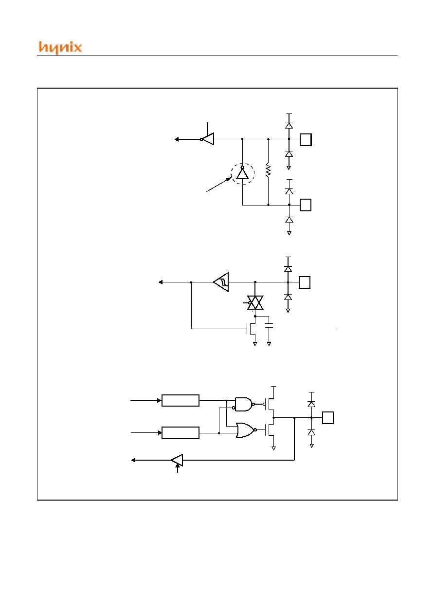
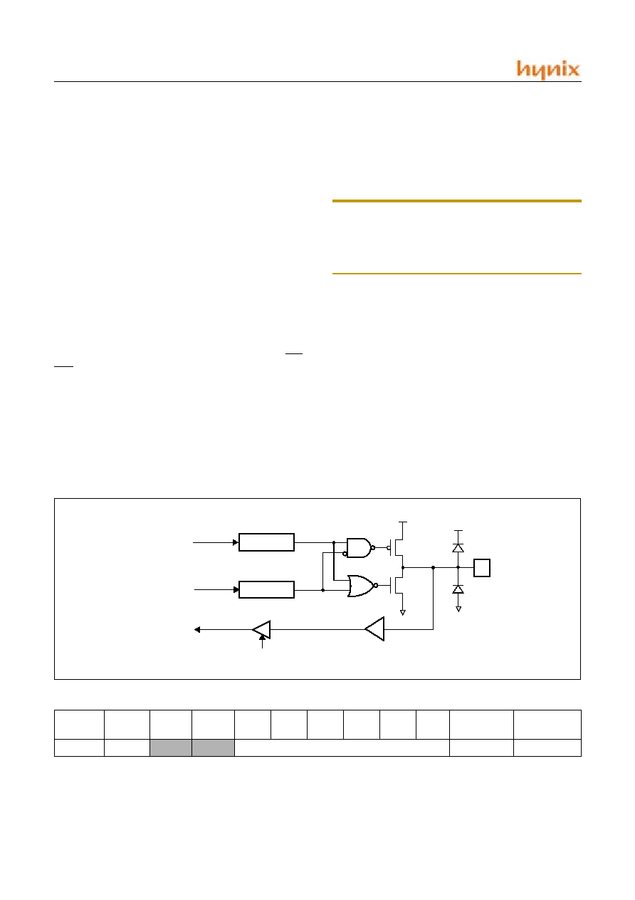
6. PORT STRUCTURES
� UP3/RESET
� UP0~UP1
� UP2/EC0
V
SS
To RESET circuit
Weak Pull-up
RESETE(configuration bit4)
UPPU(OPTION bit6)
Read UPIO
Data Bus
Data Bus
Data Bus
Data Bus
Data Reg.
Tris Reg.
Read UPIO
V
DD
V
SS
Weak Pull-up
UPPU(OPTION bit6)
Data Bus
Data Bus
Data Bus
Data Reg.
Tris Reg.
Read UPIO
V
DD
V
SS
Timer/Counter
HMS77C2000/2001
Nov. 2002 Ver 1.1
7
� UP5/Xin, UP4/Xout
V
SS
Xout
Xin
Amplifier varies with
To Internal Clock
V
DD
Xin
XT, LF Mode (X
IN
,X
OUT
)
EN ( XT, LF )
R
F
ERC Mode (X
IN
)
the oscillation mode
Internal
Capacitance ( appx. 5pF )
To Internal Clock
Enable
(ERC)
Data Bus
Data Bus
Data Bus
Data Reg.
Tris Reg.
Read UPIO
V
DD
V
SS
Normal I/O(UP4/UP5)
HMS77C2000/2001
8
Nov. 2002 Ver 1.1
7. ELECTRICAL CHARACTERISTICS
7.1 ABSOLUTE MAXIMUM RATINGS
Supply voltage .............................................. -0 to +6.5 V
Storage Temperature ................................-65 to +125
�
C
Voltage on RESET with respect to V
SS
.......0.3 to 12.5V
Voltage on any pin with respect to V
SS
. -0.3 to V
DD
+0.3
Maximum current out of V
SS
pin ........................100 mA
Maximum current into V
DD
pin ..........................100 mA
Maximum output current sunk by (I
OL
per I/O Pin)25 mA
Maximum output current sourced by (I
OH
per I/O Pin)
...............................................................................20 mA
Maximum current (
I
OL
) .................................... 100 mA
Maximum current (
I
OH
)...................................... 80 mA
Note: Stresses above those listed under "Absolute Maxi-
mum Ratings" may cause permanent damage to the
device. This is a stress rating only and functional op-
eration of the device at any other conditions above
those indicated in the operational sections of this
specification is not implied. Exposure to absolute
maximum rating conditions for extended periods
may affect device reliability.
7.2 RECOMMENDED OPERATING CONDITIONS
Parameter
Symbol
Condition
Specifications
Unit
Min.
Max.
Supply Voltage
V
DD
f
XIN
=4MHz
2.5
5.5
V
Operating Frequency
f
XIN
ERC Mode
0.2
4
MHz
IRC Mode
4
4
XT Mode
0.455
4
LF Mode
32
200
KHz
Operating Temperature
T
OPR
-40
85
�
C

HMS77C2000/2001
Nov. 2002 Ver 1.1
9
7.3 DC CHARACTERISTICS (1)
�
(T
A
=-40
�
C~+85
�
C)
Parameter
Symbol
Test Condition
Specification
Unit
Min
Typ
1
1.
Data in "Typ" column is at 25
�
C unless otherwise stated. These parameters are for design guidance only and are not tested.
Max
Supply Voltage
V
DD
2.5
5.5
V
V
DD
start voltage to ensure
Power-On Reset
V
POR
-
V
SS
-
V
V
DD
rise rate to ensure
Power-On Reset
S
VDD
2
2.
This parameter is characterized but not tested.
0.05
-
-
V/mS
RAM Data Retention
Voltage
V
DR
-
0.6
-
V
Power Fail Detection
V
PFD
2.4
2.7
3.2
V
Supply Current
I
DD
3
3.
The test conditions for all I
DD
measurements in
NOP
execution are:
X
IN
= external square wave; all I/O pins tristated, pulled to V
SS
, EC0 = V
DD
, RESET = V
DD
; WDT disabled/enabled as specified.
ERC
4
osc
4.
Does not include current through R
ext.
The current through the resistor can be estimated by the formula; I
R
= V
DD
/2R
ext
(mA)
X
IN
= 4MHz, V
DD
= 5.5V
-
1
2.5
mA
IRC osc
X
IN
= 4MHz, V
DD
= 5.5V
-
1
2.5
mA
XT osc
X
IN
= 4MHz, V
DD
= 5.5V
-
2
4
mA
LF osc
X
IN
= 32KHz, V
DD
= 3V, WDT Disabled
-
30
50
uA
Power Down Current
I
PD
5
5.
Power down current is measured with the part in SLEEP mode, with all I/O pins in hi-impedance state and tied to V
DD
and V
SS
as
like measurement conditions of supply current.
V
DD
= 3V, WDT Enabled
-
3
15
uA
V
DD
= 3V, WDT Disabled
-
0.25
14

HMS77C2000/2001
10
Nov. 2002 Ver 1.1
7.4 DC ELECTRICAL CHARACTERISTICS (2)
�
(T
A
=-40
�
C~+85
�
C)
Parameter
Symbol
Test Condition
Specification
Unit
Min
Typ
1
1.
Data in "Typ" column is at 25
�
C unless otherwise stated. These parameters are for design guidance only and are not tested.
Max
Input High Voltage
V
IH
V
I/O Ports (TTL)
2
I/O Ports (ST)
0.8V
DD
RESET, EC0, (ST)
0.8V
DD
-
V
DD
X
IN
(ST)
RC osc only
0.8V
DD
X
IN
XT, LF osc
0.7V
DD
Input Low Voltage
V
IL
V
I/O Ports (TTL)
0.6
I/O Ports (ST)
0.2V
DD
RESET, EC0, (ST)
V
SS
-
0.2V
DD
X
IN
(ST)
RC osc only
0.1V
DD
X
IN
XT, LF
0.3V
DD
Hysteresis of Schmitt
Trigger Inputs
V
HYS
0.15V
DD
2
2.
This parameter are characterized but not tested.
V
Input Leakage Current
I
L
V
SS
V
PIN
V
DD
-
-
�
5
uA
I/O Ports
Output High Voltage
V
OH
I
OH
= -3.0mA, V
DD
= 4.5V
V
DD
- 0.7
-
V
DD
V
I/O Ports
Output Low Voltage
V
OL
I
OL
= 8.5mA, V
DD
= 4.5V
V
SS
-
0.6
V
I/O Ports
Weak Pull-up current
I
PUR
V
DD
= 5.5V, V
PIN
= V
SS
uA
UP0/UP1
150
250
350
RESET
20
40
60

HMS77C2000/2001
Nov. 2002 Ver 1.1
11
7.5 AC ELECTRICAL CHARACTERISTICS (1)
� (T
A
=-40
�
C~+85
�
C)
Parameter Symbol
Test
Condition
Specification
Unit
Min
Typ
Max
External Clock Input
Frequency
F
XIN
XT osc mode
DC
-
4.0
MHz
LF osc mode
DC
-
200
KHz
Oscillator Frequency
1
1.
This parameter is characterized but not tested.
F
XIN
ERC osc mode
DC
-
4.0
MHz
XT osc mode
0.2
-
4.0
MHz
LF osc mode
32
-
200
KHz
External Clock Input
Period
T
XIN
XT osc mode
250
-
-
nS
LF osc mode
5
-
-
uS
Oscillator Period
1
T
XIN
ERC osc mode
250
-
-
nS
XT osc mode
250
-
5,000
nS
LF osc mode
5
-
-
uS
Clock in X
IN
Pin
1
Low or High Time
T
XIN
L
T
XIN
H
XT osc mode
50
-
-
nS
LF osc mode
2.0
-
-
uS
Clock in X
IN
Pin
1
Rise or Fall Time
T
XIN
R
T
XIN
F
XT osc mode
-
-
25
nS
LF osc mode
-
-
50
nS
HMS77C2000/2001
12
Nov. 2002 Ver 1.1
7.6 AC ELECTRICAL CHARACTERISTICS (2)
�
(T
A
=-40
�
C~+85
�
C)
Parameter
1
1.
These parameters are characterized but not tested.
Symbol
Test Condition
Specification
Unit
Min
Typ
2
2.
Data in "Typ" column is at 25
�
C unless otherwise stated. These parameters are for design guidance only and are not tested.
Max
RESET Pulse Width (Low)
T
RESET
V
DD
= 5V
4000
-
nS
Watchdog Timer Time-Out
Period ( No-prescaler )
T
WDT
V
DD
= 5V
9
18
30
mS
Internal Reset Timer Period
T
IRT
V
DD
= 5V, ERC/IRC
osc
9
18
30
mS
V
DD
= 5V, XT/LF osc
-
300
-
uS
Internal Calibrated RC Fre-
quency
F
IRC
V
DD
= 5V
3.6
-
4.4
MHz
EC0 High or Low Pulse Width
T
EC0
H
T
EC0
L
T
CY
= 4 X T
XIN
Instruction cycle time
nS
No Prescaler
10
-
-
With Prescaler
0.5T
CY
+ 20
-
-
EC0 Period
T
EC0
P
N
= Prescaler Value
( 1,2,4,......256 )
nS
No Prescaler
20
-
-
With Prescaler
(T
CY
+40) / N
-
-
T
XIN
R
X
IN
EC0
0.15V
0.85V
DD
0.15V
DD
RESET
0.15V
DD
0.85V
DD
T
EC0
H
T
XIN
T
RESET
T
XIN
F
T
XIN
H
T
XIN
L
T
EC0
H
T
EC0
P
HMS77C2000/2001
Nov. 2002 Ver 1.1
13
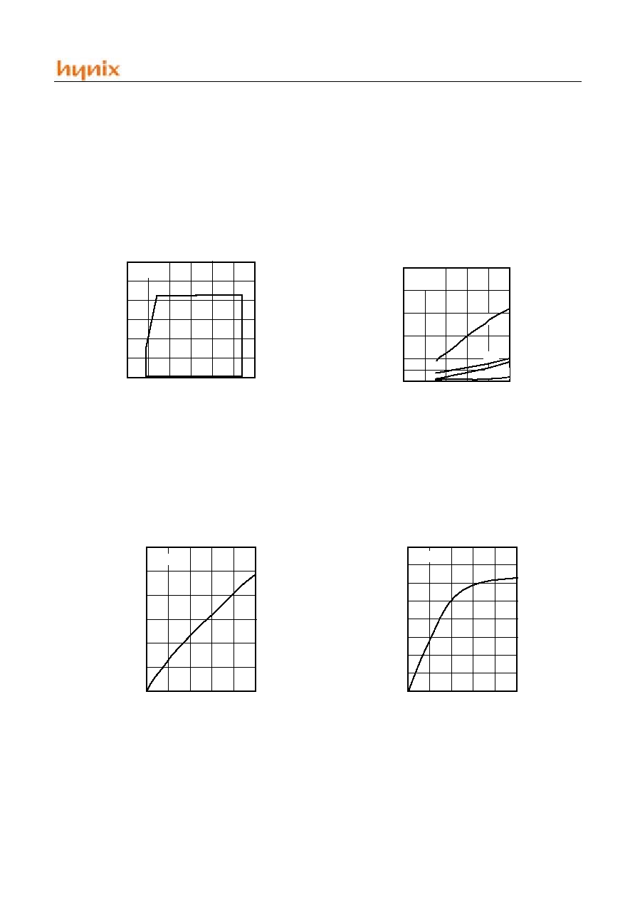
7.7 TYPICAL CHARACTERISTICS
These graphs and tables are for design guidance only and
are not tested or guaranteed.
In some graphs or tables the data presented are out-
side specified operating range (e.g. outside specified
V
DD
range). This is for information only and devices
are guaranteed to operate properly only within the
specified range.
The data is a statistical summary of data collected on units
from different lots over a period of time. "Typical" repre-
sents the mean of the distribution while "max" or "min"
represents (mean + 3
) and (mean
-
3
) respectively
where
is standard deviation
Ta= 25
�
C
Ta=25
�
C
I
DD
-
V
DD
4
3
2
1
0
(mA)
I
DD
2
3
4
5
6
V
DD
(V)
Normal Operation(Frequency=4MHz)
6
4
2
0
0
(MHz)
f
XIN
2
3
4
5
6
Operating Area
XT
10
8
32KHz
I
OL
-
V
OL
, V
DD
=5.5V
32
24
16
8
0
(mA)
I
OL
V
OL
(V)
0.4
0.8
1.2
1.6
2.0
40
I
OL
-
V
OL
, V
DD
=2.5V
12
8
4
0
(mA)
I
OL
V
OL
(V)
0.4
0.8
1.2
1.6
2.0
Ta=25
�
C
Ta=25
�
C
IRC
ERC
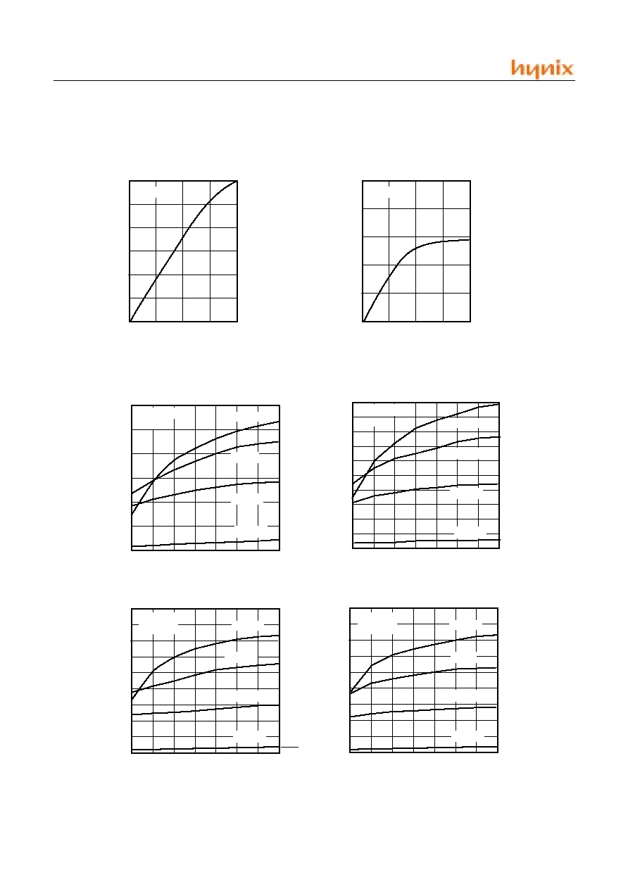
HMS77C2000/2001
14
Nov. 2002 Ver 1.1
I
OH
-
V
OH
, V
DD
=5.5V
-16
-12
-8
-4
0
(mA)
I
OH
0.5
1.0
1.5
V
DD
-V
OH
(V)
-20
I
OH
-
V
OH
, V
DD
=2.5V
-6
-4
-2
0
(mA)
I
OH
0.5
1.0
1.5
-8
2.0
V
DD
-V
OH
(V)
Typical RC Oscillator
4.5
3.0
1.5
0
(MHz)
F
OSC
2.5
3
4
5
6
V
DD
(V)
Frequency
VS
. V
DD
7.5
6.0
3.5
4.5
5.5
Ta=25
�
C
R=3.3K
R=5K
R=10K
R=100K
Typical RC Oscillator
3.0
2.5
2.0
0
(MHz)
F
OSC
2.5
3
4
5
6
V
DD
(V)
Frequency
VS
. V
DD
4.5
3.5
3.5
4.5
5.5
R=3.3K
R=10K
0.5
1.0
1.5
R=5K
Typical RC Oscillator
1.50
1.25
1.00
0
(MHz)
F
OSC
2.5
3
4
5
6
V
DD
(V)
Frequency
VS
. V
DD
2.00
1.75
3.5
4.5
5.5
R=3.3K
R=10K
0.25
0.50
0.75
R=5K
Cext=0pF
Ta=25
�
C
Cext=20pF
Ta=25
�
C
Cext=100pF
4.0
R=100K
R=100K
Typical RC Oscillator
0.6
0.5
0.4
0
(MHz)
F
OSC
2.5
3
4
5
6
V
DD
(V)
Frequency
VS
. V
DD
0.8
0.7
3.5
4.5
5.5
R=3.3K
R=10K
0.1
0.2
0.3
R=5K
Ta=25
�
C
Cext=300pF
R=100K
Ta=25
�
C
Ta=25
�
C
2.0
HMS77C2000/2001
Nov. 2002 Ver 1.1
15
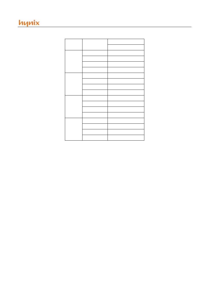
Cext
Rext
Average
Fosc @ 5V,25
�
C
0pF
3.3K
7.48MHz
5K
6.36MHz
10K
4.04MHz
100K
529KHz
20pF
3.3K
4.60MHz
5K
3.62MHz
10K
2.14MHz
100K
249KHz
100pF
3.3K
1.75MHz
5K
1.31MHz
10K
734KHz
100K
80KHz
300pF
3.3K
702KHz
5K
510KHz
10K
283KHz
100K
30KHz
Table 7-1 RC Oscillator Frequencies
HMS77C2000/2001
16
Nov. 2002 Ver 1.1
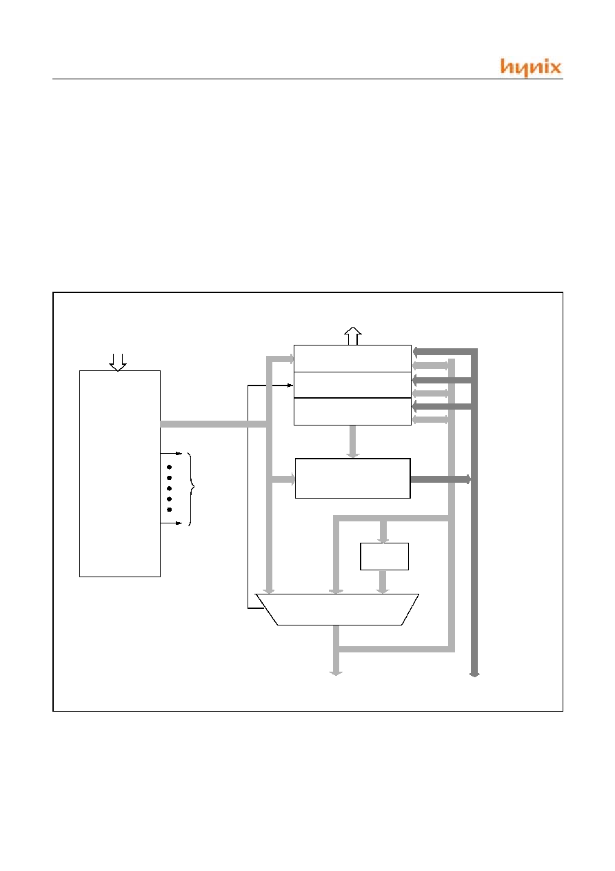
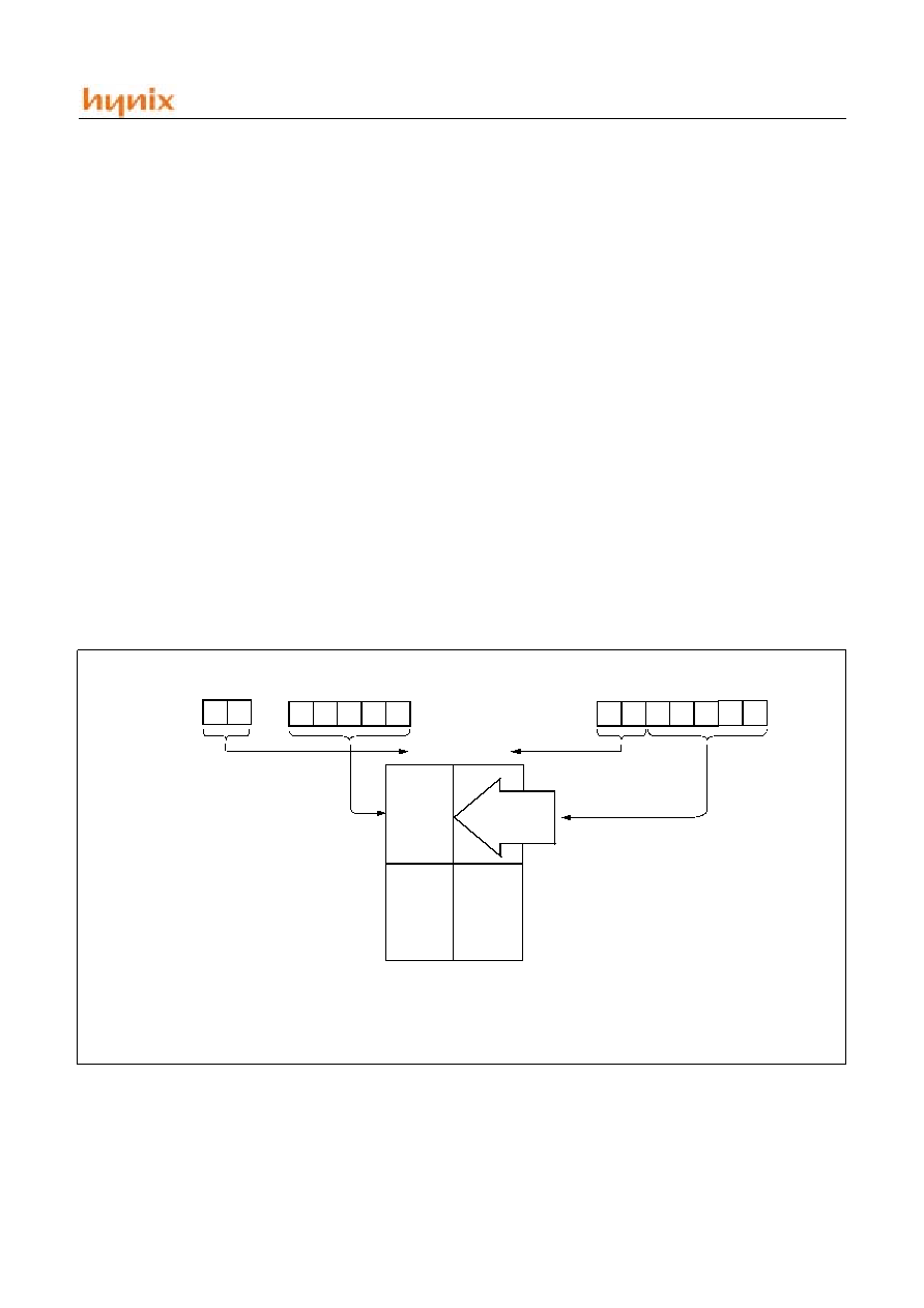
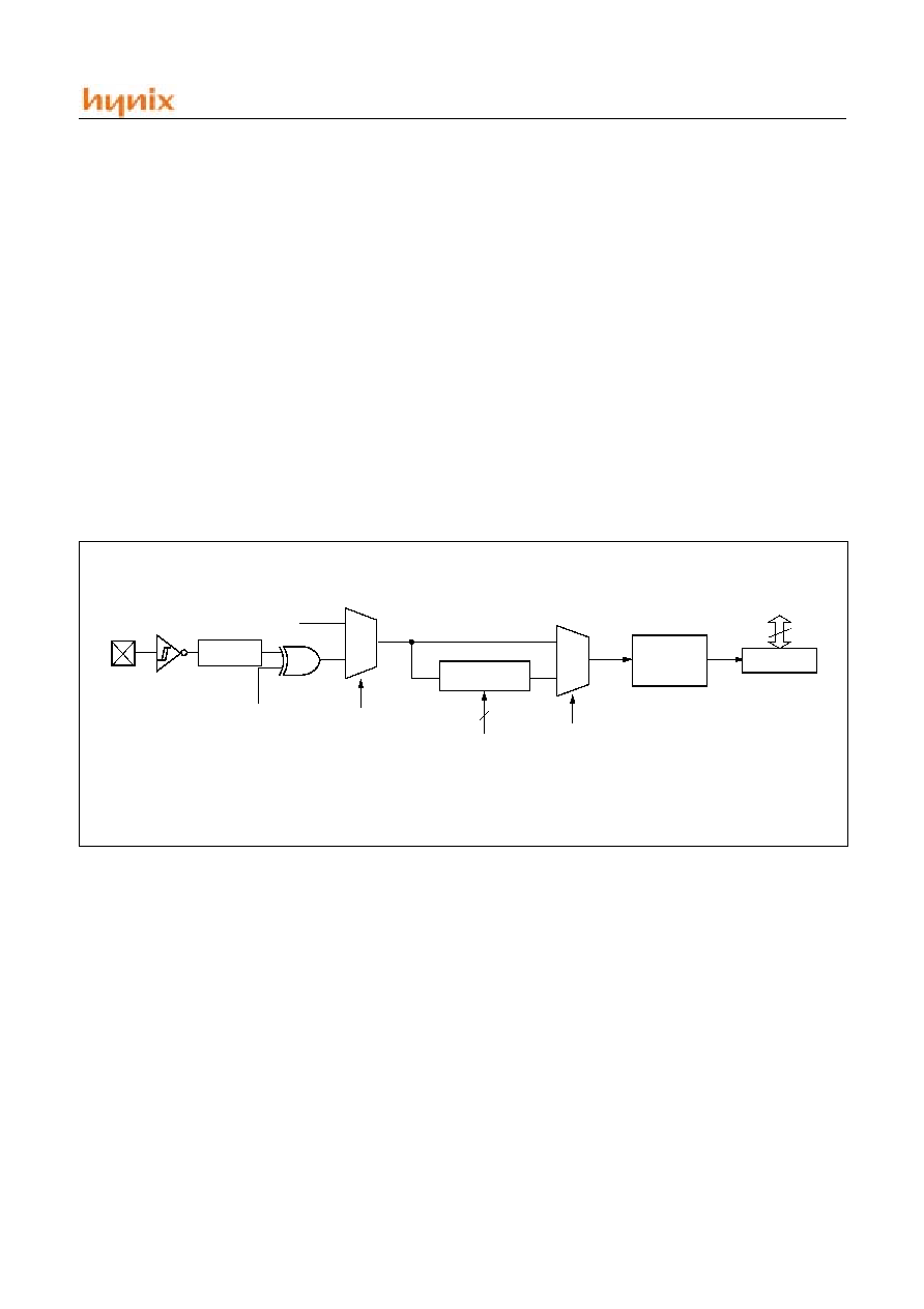
8. ARCHITECTURAL OVERVIEW
8.1 CPU ARCHITECTURE
The GMS700 core is a RISC-based CPU and uses a modi-
fied Harvard architecture. This architecture uses two sepa-
rate memories with separate address buses, one for the
program memory and the other for the data memory. This
architecture adapts 33 single word instructions that are 12-
bit wide instruction and has an internal 2-stage pipeline
(fetch and execute), which results in execution of one in-
struction per single cycle(1uS@ 4MHz) except for pro-
gram branches.
The HMS77C2000 and HMS77C2001can address 0.5K/
1K x 12 Bits program memory and 25/41 Bytes data mem-
ory. And it can directly or indirectly address data memory.
The GMS700 core has three special function registers PC,
STATUS and FSR in data memory map and has ATU (Ad-
dress Translation Unit) to provide address for data memory
and has an 8-bit general purpose ALU and working regis-
ter(W) as an accumulator. The W register consists of 8-bit
register and it can not be an addressed register.
FIGURE 8-1 GMS700 CPU BLOCK DIAGRAM
Instruction
Decode
&
Control
Unit
STATUS
FSR
W
ALU
Instruction
Program Memory Address
Immediate Data
Data Bus
Data Memory Bus
Indirect Address
Address Translation
Unit
PC with 2-level Stack
Control
Signals
ALU
Status
HMS77C2000/2001
Nov. 2002 Ver 1.1
17
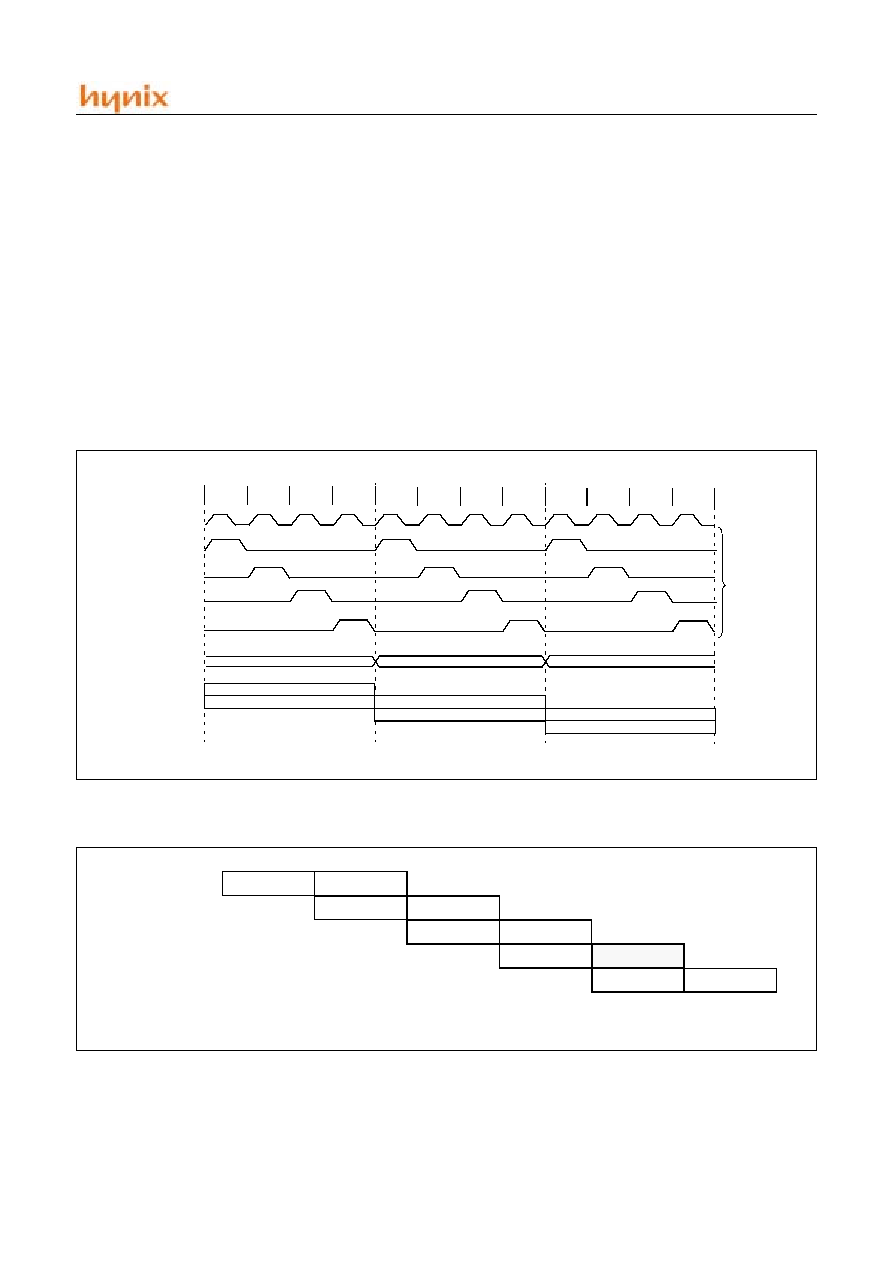
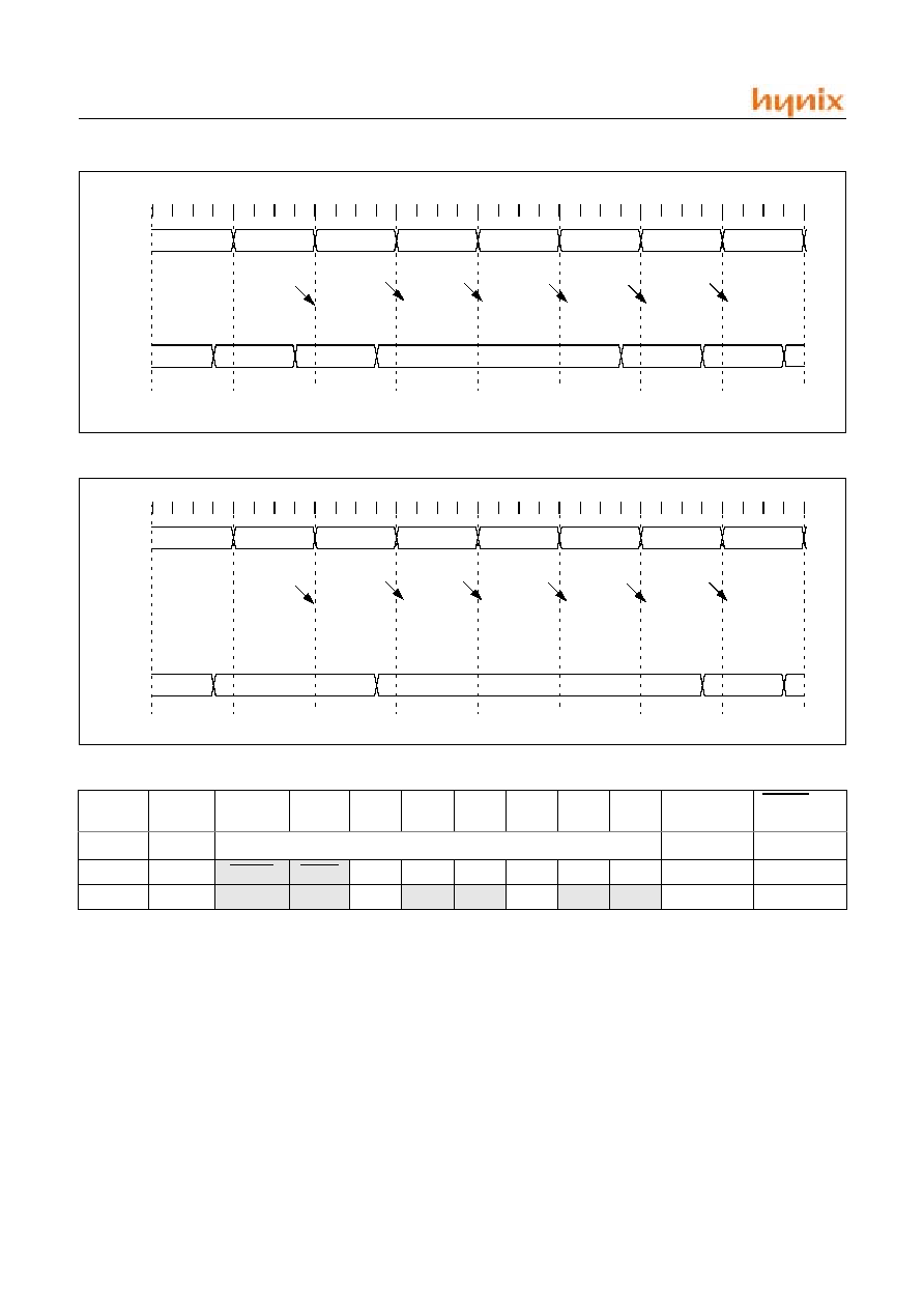
8.2 CLOCKING SCHEME/INSTRUCTION
CYCLE
The clock input (X
IN
pin) is internally divided by four to
generate four non-overlapping quadrature clocks namely
Q1, Q2, Q3 and Q4. Internally, the program counter is in-
cremented every Q1, and the instruction is fetched from
program memory and latched into instruction register in
Q4. It is decoded and executed during the following Q1
through Q4. The clocks and instruction execution flow is
shown in Figure 8-2 and Figure 8-3.
8.3 INSTRUCTION FLOW/PIPELINING
An Instruction Cycle consists of four Q cycles (Q1, Q2, Q3
and Q4). The instruction fetch and execute are pipelined
such that fetch takes one instruction cycle while decode
and execute takes another instruction cycle. However, due
to the pipelining, each instruction effectively executes in
one cycle. If an instruction causes the program counter to
change (e.g.,
GOTO
) then two cycles are required to com-
plete the instruction (Figure 8-3).
A fetch cycle begins with the program counter (PC) incre-
menting in Q1.
In the execution cycle, the fetched instruction is latched
into the Instruction Register (IR) in cycle Q1. This instruc-
tion is then decoded and executed during the Q2, Q3, and
Q4 cycles. Data memory is read during Q2 (operand read)
and written during Q4 (destination write).
FIGURE 8-2 CLOCK/INSTRUCTION CYCLE
Internal
Q1
Q2
Q3
Q4
Q1
Q2
Q3
Q4
Q1
Q2
Q3
Q4
Fetch INST(PC)
Execute INST(PC-1)
Fetch INST(PC+1)
Execute INST(PC)
Fetch INST(PC+2)
Execute INST(PC+1)
PC
PC+1
PC+2
PC
Q4
Q3
Q2
Q1
X
IN
Phase
clock
FIGURE 8-3 INSTRUCTION PIPELINE FLOW
All instructions are single cycle, except for any program branches. These take two cycles since the fetch instruction is "flushed"
from the pipeline while the new instruction is being fetched and then executed.
1. MOVLW 03H
2. MOVWF UPIO
3. CALL SUB_1
4. BSF UPIO, BIT1
Fetch 1
Execute 1
Fetch 2
Execute 2
Fetch 3
Execute 3
Fetch 4
Flush
Fetch SUB 1
Execute SUB 1
HMS77C2000/2001
18
Nov. 2002 Ver 1.1
9. MEMORY ORGANIZATION
The HMS77C2000 and HMS77C2001 memories are orga-
nized into program memory and data memory. For devices
with more than 512 bytes of program memory, a paging
scheme is used. Program memory pages are accessed using
one STATUS register bit. For the HMS77C2001 with a
data memory register file of more than 32 registers, a bank-
ing scheme is used. Data memory banks are accessed using
the File Select Register (FSR).
9.1 PROGRAM MEMORY ORGANIZATION
The HMS77C2000 and HMS77C2001 devices have a 12-
bit program counter (PC) capable of addressing a 0.5K/1K
x 12 program memory space.
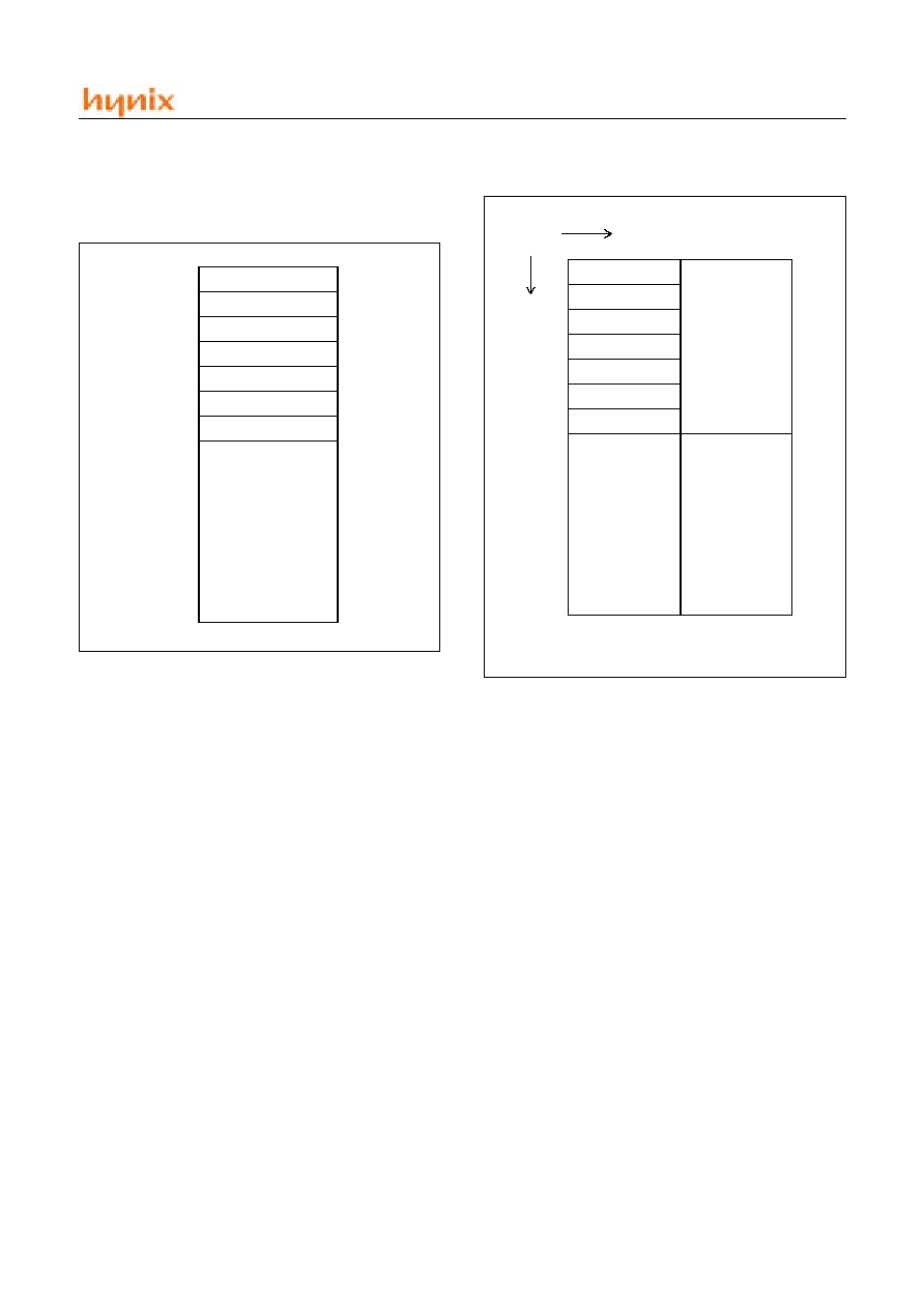
Only the first 512 x 12bits(0000
H
~01FF
H
) for the
HMS77C2000 and 1K x 12bits(0000
H
-03FF
H
) for the
HMS77C2001 are physically implemented. Refer to Fig-
ure 9-1, Figure 9-2. Accessing a location above these
boundaries will cause a wraparound within the first 512 x
1 2 s p a c e ( H M S 7 7 C 2 0 0 0 ) o r 1 K x 1 2
space(HMS77C2001). The effective reset vector is at
000
H
, (see Figure 9-1, Figure 9-2). Location 01FF
H
(HMS77C2000) or location 03FF
H
(HMS77C2001) con-
tains the internal clock oscillator calibration value. This
value should never be overwritten.
9.2 DATA MEMORY ORGANIZATION
Data memory is composed of registers, or bytes of RAM.
Therefore, data memory for a device is specified by its reg-
ister file. The register file is divided into two functional
groups: special function registers and general purpose reg-
isters.
The special function registers include the TMR0 register,
the program counter (PC), the status register, the I/O regis-
ters (ports), and the file select register (FSR). In addition,
special purpose registers are used to control the I/O port
configuration and prescaler options.
The general purpose registers are used for data and control
information under command of the instructions.
For the HMS77C2000 the register file is composed of 7
special function registers and 25 general purpose registers
(Figure 9-3).
For the HMS77C2001 the register file is composed of 7
special function registers, 25 general purpose registers, and
16 general purpose registers that may be addressed using a
banking scheme (Figure 9-4).
FIGURE 9-1 HMS77C2000 PROGRAM MEMORY MAP
AND STACK
PC<8:0>
Stack Level 1
Stack Level 2
Reset Vector
On-chip
Program
Memory
000
H
0FF
H
100
H
1FF
H
User Memory
Spa
c
e
FIGURE 9-2 HMS77C2001 PROGRAM MEMORY MAP
AND STACK
PC<9:0>
Stack Level 1
Stack Level 2
Reset Vector
On-chip
Program
Memory
000
H
0FF
H
100
H
3FF
H
U
s
er Memory
Space
On-chip
Program
Memory
2FF
H
300
H
1FF
H
200
H
(Page 0)
(Page 1)
HMS77C2000/2001
Nov. 2002 Ver 1.1
19
9.2.1 General Purpose Register File
The general purpose register file is accessed either directly
or indirectly through the file select register FSR.
FIGURE 9-3 HMS77C2000 REGISTER FILE MAP
00
H
01
H
02
H
03
H
04
H
05
H
06
H
1F
H
INDF
1
1. Not a physical register
TMR0
PCL
STATUS
FSR
OSCCAL
UPIO
Universal
Purpose
Register
FIGURE 9-4 HMS77C2001 REGISTER FILE MAP
00
H
01
H
02
H
03
H
04
H
05
H
06
H
1F
H
INDF
1
1. Not a physical register
TMR0
PCL
STATUS
FSR
OSCCAL
UPIO
Universal
Purpose
Register
File Address
FSR<6:5>
00
Universal
Purpose
Register
Addressed map
back to addresses
in Bank 0.
01
Bank 0
Bank 1
HMS77C2000/2001
20
Nov. 2002 Ver 1.1
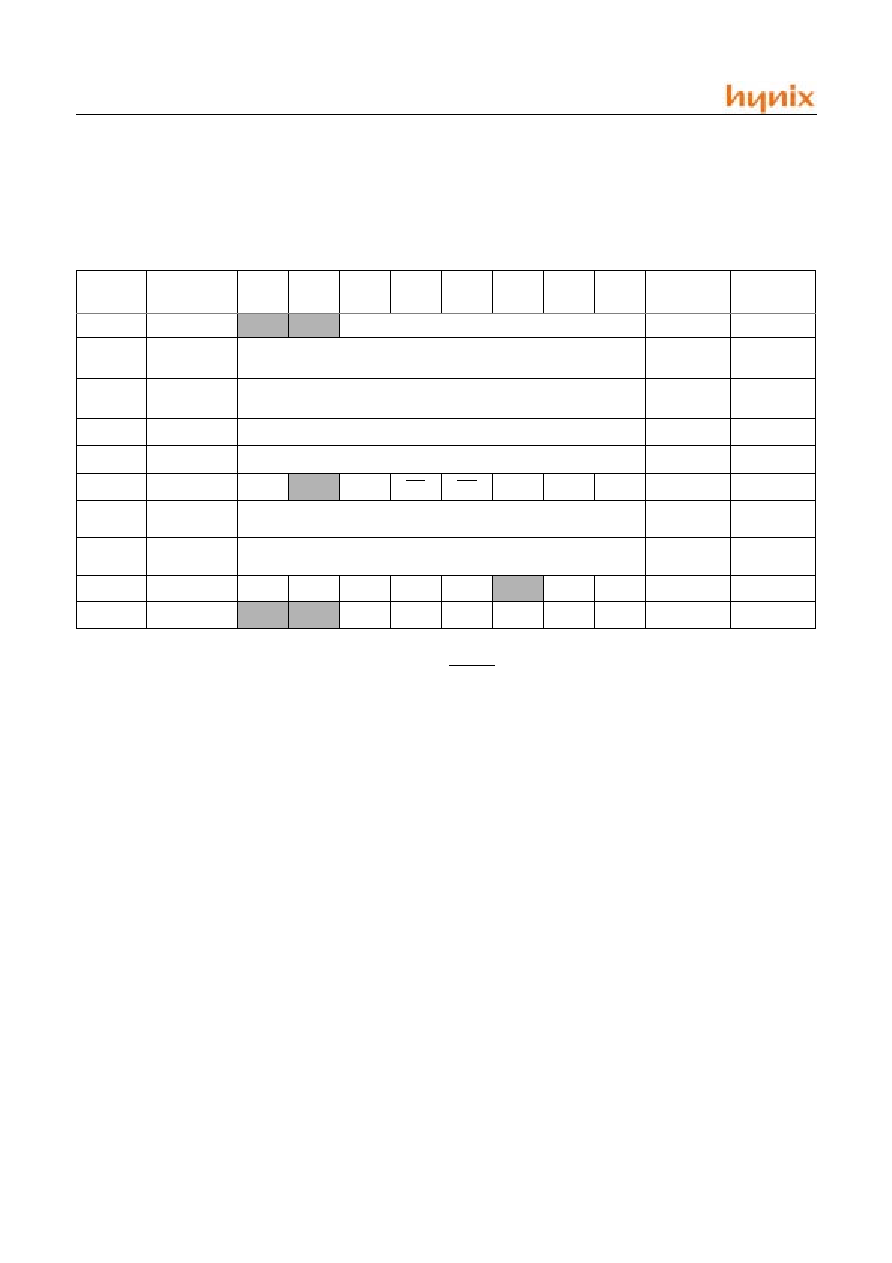
9.2.2 SPECIAL FUNCTION REGISTERS
The Special Function Registers (SFRs) are registers used
by the CPU and peripheral functions to control the opera-
tion of the device (Table 9-1).
The special registers can be classified into two sets. The
special function registers associated with the "core" func-
tions are described in this section. Those related to the op-
eration of the peripheral features are described in the
section for each peripheral feature.
Legend: Shaded boxes = unimplemented or unused, - = unimplemented, read as `0' (if applicable)
x = unknown, u = unchanged, q = see the tables in Section 12.7 for possible values.
Address
Name
Bit7
Bit6
Bit5
Bit4
Bit3
Bit2
Bit1
Bit0
Power-On
Reset
All other
resets
1
N/A
TRIS
-
-
I/O control registers
--11 1111
--11 1111
N/A
OPTION
Contains control bits to configure Timer0, Timer0/WDT prescaler,
wake-up change, weak pull-up
1111 1111
1111 1111
00
H
INDF
Uses contents of FSR to address data memory (not a physical reg-
ister)
xxxx xxxx
uuuu uuuu
01
H
TMR0
8-bit real-time clock/counter
xxxx xxxx
uuuu uuuu
02
H
2
PCL
Low order 8bits of PC
1111 1111
1111 1111
03
H
STATUS
UPWUF
-
PA0
TO
PD
Z
DC
C
0001 1xxx
q00q quuu
3
04
H
FSR
(HMS77C2000)
Indirect data memory address pointer
111x xxxx
111u uuuu
04
H
FSR
(HMS77C2001)
Indirect data memory address pointer
110x xxxx
11uu uuuu
05
H
OSCCAL
CAL4
CAL3
CAL2
CAL1
CAL0
-
PFDF
PFDEN
1000 0000
1000 0000
06
H
UPIO
-
-
UP5
UP4
UP3
UP2
UP1
UP0
--xx xxxx
--uu uuuu
TABLE 9-1 SPECIAL FUNCTION REGISTER SUMMARY
1. Other (non power-up) resets include external reset through RESET, watchdog timer and wake-up on pin change reset.
2. The upper byte of the Program Counter is not directly accessible. See Section 9.6 for an explanation of how to access
these bits.
3. If reset was due to wake-up on pin change then bit 7 = 1. All other resets will cause bit 7 = 0.
HMS77C2000/2001
Nov. 2002 Ver 1.1
21
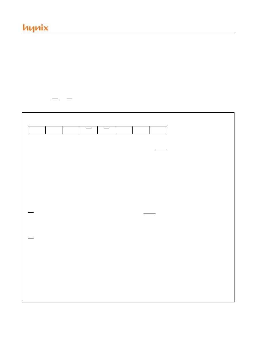
9.3 STATUS REGISTER
This register contains the arithmetic status of the ALU, the
RESET status, and the page preselect bit for program
memories larger than 512 words.
The STATUS register can be the destination for any in-
struction, as with any other register. If the STATUS regis-
ter is the destination for an instruction that affects the Z,
DC or C bits, then the write to these three bits is disabled.
These bits are set or cleared according to the device logic.
Furthermore, the TO and PD bits are not writable. There-
fore, the result of an instruction with the STATUS register
as destination may be different than intended.
For example,
CLRF STATUS
will clear the upper three
bits and set the Z bit. This leaves the STATUS register as
000u u1uu (where u = unchanged).
It is recommended, therefore, that only
BCF
,
BSF
and
MOVWF
instructions be used to alter the STATUS register
because these instructions do not affect the Z, DC or C bits
from the STATUS register. For other instructions, which
do affect STATUS bits, see Instruction Set Summary.
9.4 OPTION REGISTER
The OPTION register is a 8-bit wide, write-only register
FIGURE 9-5 STATUS REGISTER
-
PA0
R/W
TO
R
PD
R
Z
R/W
DC
R/W
C
R/W
bit7
bit0
UPWUF: UPIO reset bit
1 = Reset due to wake-up from SLEEP on pin
change
0 = After power up or other reset
- : Unimplemented
PA0: Program memory page select bits
0 = page 0 (000h - 1FFh) - GMS77C1000/1001
1 = page 1 (200h - 3FFh) - GMS77C1001
TO: Time-overflow bit
1 = After power-up, watchdog clear instruction, or
entering power-down mode
0 = A watchdog timer time-overflow occurred
PD: Power-down bit
1 = After power-up or by the watchdog clear
instruction
0 = By execution of power-down mode
Z: Zero bit
1 = The result of an arithmetic or logic operation
is zero
0 = The result of an arithmetic or logic operation
is not zero
DC: Digit carry/borrow bit
(for addition and subtraction)
addition
1 = A carry from the 4th low order bit of the result
occurred
0 = A carry from the 4th low order bit of the result
did not occur
subtraction
1 = A borrow from the 4th low order bit of the
result did not occur
0 = A borrow from the 4th low order bit of the
result occurred
C: Carry/borrow bit
(for additon,subtraction and rotation)
addition
1 = A carry occurred
0 = A carry did not occur
subtraction
1 = A borrow did not occur
0 = A borrow occurred
rotation
Load bit with LSB or MSB, respectively
R = Readable bit
W = Writable bit
ADDRESS ; 03
H
RESET VALUE : 0001_1XXX
UPWUF
R
HMS77C2000/2001
22
Nov. 2002 Ver 1.1
which contains various control bits to configure the
Timer0/WDT prescaler and Timer0.
By executing the
OPTION
instruction, the contents of the
W register will be transferred to the OPTION register. A
RESET sets the OPTION<7:0> bits.
Note: If TRIS bit is set to `0', the wake-up on change and
pull-up functions are disabled for that pin; i.e., note
that TRIS overrides OPTION control of UPPU and
UPWU.
If the T0CS bit is set to `1', UP2 is forced to be an
input even if TRIS UP2 = `0'.
FIGURE 9-6 OPTION REGISTER
UPWU
W
UPPU
W
T0CS
W
T0SE
W
PSA
W
PS2
W
PS1
W
PS0
W
bit7
6
bit0
5
4
3
2
1
UPWU: Enable wake-up on pin change
(UP0, UP1, UP3)
1 = Disabled
0 = Enabled
UPPU: Enable weak pull-ups (UP0, UP1, UP3)
1 = Disabled
0 = Enabled
T0CS: Timer 0 clock source select bit
1 = Transition on EC0 pin
0 = Transition on internal instruction cycle,
F
OSC
/4
T0SE: Timer 0 source edge select bit
1 = Increment on high to low transition
on EC0 pin
0 = Increment on low to high transition
on EC0 pin
PSA: Prescaler assignment bit
1 = Prescaler assigned to the WDT
0 = Prescaler assigned to the Timer 0
PS2~PS0: Prescaler rate select bits)
Bit Value
Timer 0 rate
WDT rate
000
1:2
1:1
001
1:4
1:2
010
1:8
1:4
011
1:16
1:8
100
1:32
1:16
101
1:64
1:32
110
1:128
1:64
111
1:256
1:128
W = Writable bit
-n = Value at POR reset
ADDRESS ; N/A
RESET VALUE : 1111_1111
HMS77C2000/2001
Nov. 2002 Ver 1.1
23
9.5 OSCCAL REGISTER
The oscillator calibration (OSCCAL) register is used to
calibrate the internal 4 MHz oscillator. It contains five bits
for calibration. Increasing the cal value increases the fre-
quency.
Also it controls power fail detection circuit by the lower
2bits.
9.6 PROGRAM COUNTER
As a program instruction is executed, the program counter
(PC) will contain the address of the next program instruc-
tion to be executed. The PC value is increased by one every
instruction cycle, unless an instruction changes the PC.
For a
GOTO
instruction, bits 8~0 of the PC are provided
by the
GOTO
instruction word. The PC Latch (PCL) is
mapped to PC<7~0>. Bit 5 of the STATUS register pro-
vides page information to bit 9 of the PC (Figure 9-8).
For a
CALL
instruction, or any instruction where the PCL
is the destination, bits 7~0 of the PC again are provided by
the instruction word. However, PC<8> does not come
from the instruction word, but is always cleared (Figure 9-
8).
Instructions where the PCL is the destination, or Modify
PCL instructions, include
MOVWF PC, ADDWF PC,
and
BSF PC,5.
Note: Because PC<8> is cleared in the
CALL
instruction,
or any Modify PCL instruction, all subroutine calls or
computed jumps are limited to the first 256 locations
of any program memory page (512 words long).
FIGURE 9-7 OSCCAL REGISTER
CAL4
R/W
CAL3
R/W
CAL2
R/W
CAL1
R/W
CAL0
R/W
-
R/W
PFDF
R/W
PFDEN
R/W
bit7
6
bit0
5
4
3
2
1
CAL4~CAL0: Calibration Bits
11111 = High frequency
10000 = Middle frequency
00000 = Low frequency
PFDF: Power-fail detection flag bit.
1 = Reset caused by PFD reset.
0 = PFD reset is not generated.
PFDEN: Power-fail detection enable bit
1 = Enable PFD
0 = Disable PFD
R = Readable bit
W = Writable bit
ADDRESS ; 05
H
RESET VALUE : 1000_0000
GOTO
Instruction
CALL
or Modify PCL Instruction
FIGURE 9-8 LOADING OF PC BRANCH INSTRUCTION
PCL
PC
7
0
Instruction Word
8
9
10
11
7
0
PA0
STATUS
Reset to `0'
PCL
PC
7
0
Instruction Word
8
9
10
11
7
0
STATUS
PA0

HMS77C2000/2001
24
Nov. 2002 Ver 1.1
9.6.1 EFFECTS OF RESET
The program counter is set upon a RESET, which means
that the PC addresses the last location in the last page i.e.,
the oscillator calibration instruction. After executing
MOVLW XX
, the PC will roll over to location 00
H
, and be-
gin executing user code.
The STATUS register page preselect bits are cleared upon
a RESET, which means that page 0 is preselected.
Therefore, upon a RESET, a
GOTO
instruction will auto-
matically cause the program to jump to page 0 until the val-
ue of the page bits is altered.
9.7 STACK
The HMS77C2000 and HMS77C2001 devices have a 12-
bit wide L.I.F.O. hardware push/pop stack.
A
CALL
instruction will push the current value of stack
into stack 2 and then push the current program counter val-
ue, incremented by one, into stack level 1. If more than two
sequential `
CALL
's are executed, only the most recent two
return addresses are stored.
A
RETLW
instruction will pop the contents of stack level
into the program counter and then copy stack level 2 con-
tents into level 1. If more than two sequential `
RETLW
's
are executed, the stack will be filled with the address pre-
viously stored in level 2. Note that the W register will be
loaded with the literal value specified in the instruction.
This is particularly useful for the implementation of data
look-up tables within the program memory.
Upon any reset, the contents of the stack remain un-
changed, however the program counter (PCL) will also be
reset to 0.
Note: There are no STATUS bits to indicate stack over-
flows or stack underflow conditions.
There are no instructions mnemonics called PUSH
or POP. These are actions that occur from the exe-
cution of the
CALL
and
RETLW
instructions.
FIGURE 9-9 PROGRAM COUNTER
Bit 9 :
Page select bit, provided by PA0 bit of STATS register (HMS77C2001)
1 = Page 1 (200
H
~ 3FF
H
)
0 = Page 0 (000
H
~ 1FF
H
)
Bit 8 :
Half-page select bit, provided by
GOTO
instruction (HMS77C2000, HMS77C2001)
or cleared when
CALL
or any modify-PCL instruction are executed.
1 = Half page 1 (200
H
~ 2FF
H
)
0 = Half page 0 (000
H
~ 0FF
H
)
Bit 7 ~ 0 : PCL register
Device
HMS77C2000
HMS77C2001
-
PC8
Bit 9 Bit 8 Bit 7 Bit 6 Bit 5 Bit 4 Bit 3 Bit 2 Bit 1 Bit 0 Value on reset Value after reset
PCL
PCL
01 1111 1111
11 1111 1111
11 1111 1111
11 1111 1111
PC8
PC9
HMS77C2000/2001
Nov. 2002 Ver 1.1
25
9.8 INDIRECT DATA ADDRESSING; INDF
AND FSR REGISTERS
The INDF register is not a physical register.
Addressing INDF actually addresses the register whose ad-
dress is contained in the FSR register (FSR is a pointer).
This is indirect addressing.
EXAMPLE 4-1: INDIRECT ADDRESSING
- Register file 07 contains the value 10
H
- Register file 08 contains the value 0A
H
- Load the value 07 into the FSR register
A read of the INDF register will return the value
of 10
H
- Increment the value of the FSR register by one
(FSR = 08)
- A read of the INDR register now will return the
value of 0A
H
Reading INDF itself indirectly (FSR = 0) will produce
00
H
. Writing to the INDF register indirectly results in a no-
operation (although STATUS bits may be affected).
A simple program to clear RAM locations 10
H
~1F
H
using
indirect addressing is shown in Example 4-2.
EXAMPLE 4-2: HOW TO CLEAR RAM
USING INDIRECT ADDRESSING
movlw 0x10
;initialize
pointer
movwf FSR
; to RAM
NEXT
clrf INDF
;clear INDF
register
incf FSR,F
;inc pointer
btfsc FSR,4
;all done?
goto NEXT
;NO, clear next
CONTINUE
: ;YES,
continue
The FSR is a 5-bit wide register. It is used in conjunction
with the INDF register to indirectly address the data mem-
ory area.
The FSR<4:0> bits are used to select data memory ad-
dresses 00
H
to 1F
H
.
HMS77C2000: Does not use banking. FSR<7:5> are un-
implemented and read as '1's.
HMS77C2001: Uses FSR<5>. Selects between bank 0 and
bank 1. FSR<7:6> is unimplemented, read as `1'
.
FIGURE 9-10 DIRECT/INDIRECT ADDRESSING
6
0
4
0
(opcode)
(FSR)
location
select
location
select
Data
Memory
1
00
H
0F
H
10
H
1F
H
Direct Addressing
Indirect Addressing
5
4
Addresses
map back to
address
in Bank 0.
01
00
Bank 1
2
Bank 0
1. For register map detail see Section 4.2.
2. HMS77C2001
6
5
(FSR)
bank
bank
select
HMS77C2000/2001
26
Nov. 2002 Ver 1.1
10. I/O PORT
As with any other register, the I/O register can be written
and read under program control. However, read instruc-
tions (e.g.,
MOVF UPIO,W
) always read the I/O pins inde-
pendent of the pin's input/output modes. On RESET, all I/
O ports are defined as input (inputs are at hi-impedance)
since the I/O control registers are all set.
10.1 UPIO
UPIO is an 8-bit I/O register. Only the low order 6 bits are
used (UP5:UP0). Bits 7 and 6 are unimplemented and read
as '0's. Please note that UP3 is an input only pin. The con-
figuration word can set several I/O's to alternate func-
tions. When acting as alternate functions the pins will read
as `0' during port read. Pins UP0, UP1, and UP3 can be
configured with weak pull-ups and also with wake-up on
change. The wake-up on change and weak pull-up func-
tions are not pin selectable. If pin 4 is configured as RE-
SET, weak pullup is always on and wake-up on change for
this pin is not enabled.
10.2 TRIS REGISTER
The output driver control register is loaded with the con-
tents of the W register by executing the TRIS f instruction.
A '1' from a TRIS register bit puts the corresponding output
driver in a hi-impedance mode.
A '0' puts the contents of the output data latch on the select-
ed pins, enabling the output buffer. The exceptions are
UP3 which is input only and UP2 which may be controlled
by the option register, see Figure 9-6.
Note: A read of the ports reads the pins, not the output
data latches. That is, if an output driver on a pin is
enabled and driven high, but the external system is
holding it low, a read of the port will indicate that the
pin is low.
The TRIS registers are "write-only" and are set (output
drivers disabled) upon RESET.
10.3 I/O INTERFACING
The equivalent circuit for an I/O port pin is shown in Fig-
ure 10-1. All port pins, except UP3 which is input only,
may be used for both input and output operations.
For input operations these ports are non-latching. Any in-
put must be present until read by an input instruction e.g.,
MOVF UPIO,W
). The outputs are latched and remain un-
changed until the output latch is rewritten. To use a port pin
as output, the corresponding direction control bit in TRIS
must be cleared (=0). For use as an input, the correspond-
ing TRIS bit must be set. Any I/O pin (except UP3) can be
programmed individually as input or output.
FIGURE 10-1 EQUIVALENT CIRCUIT FOR A SINGLE I/O PIN
Address
Name
Bit7
Bit6
Bit5
Bit4
Bit3
Bit2
Bit1
Bit0
Power-On
Reset
All other
Resets
N/A
TRIS
I/O control registers
--11 1111
--11 1111
TABLE 10-1 SUMMARY OF PORT REGISTERS
Legend: Shaded boxes = unimplemented or unused, - = unimplemented, read as `0', x = unknown, u = unchanged.
Data Bus
Data Bus
Data Bus
Data Reg.
TRIS Reg.
Read
V
DD
V
SS

HMS77C2000/2001
Nov. 2002 Ver 1.1
27
10.4 I/O PROGRAMMING CONSIDERATIONS
10.4.1 BI-DIRECTIONAL I/O PORTS
Some instructions operate internally as read followed by
write operations. The
BCF
and
BSF
instructions, for exam-
ple, read the entire port into the CPU, execute the bit oper-
ation and re-write the result. Caution must be used when
these instructions are applied to a port where one or more
pins are used as input/outputs. For example, a
BSF
opera-
tion on bit5 of UPIO will cause all eight bits of UPIO to be
read into the CPU, bit5 to be set and the UPIO value to be
written to the output latches. If another bit of UPIO is used
as a bidirectional I/O pin (say bit0) and it is defined as an
input at this time, the input signal present on the pin itself
would be read into the CPU and rewritten to the data latch
of this particular pin, overwriting the previous content. As
long as the pin stays in the input mode, no problem occurs.
However, if bit0 is switched into output mode later on, the
content of the data latch may now be unknown.
Example 5-1 shows the effect of two sequential read-mod-
ify-write instructions (e.g.,
BCF
,
BSF
, etc.) on an I/O port.
pin actively outputting a high or a low should not be driven
from external devices at the same time in order to change
the level on this pin ("wired-or", "wired-and"). The result-
ing high output currents may damage the chip.
EXAMPLE 5-1: READ-MODIFY-WRITE INSTRUC-
TIONS ON AN I/O PORT
;Initial UPIO Settings
;UPIO<5:3> Inputs
;UPIO<2:0> Outputs
;
;
UPIO latch UPIO pins
;
---------- ----------
BCF UPIO, 5 ;--01 -ppp --11 pppp
BCF UPIO, 4 ;--10 -ppp --11 pppp
MOVLW 007h ;
TRIS UPIO ;--10 -ppp --11 pppp
;
;Note that the user may have expected the
;pin values to be --00 pppp. The 2nd BCF
;caused UP5 to be latched as the pin value
(High).
10.4.2 SUCCESSIVE OPERATIONS ON I/O
PORTS
The actual write to an I/O port happens at the end of an in-
struction cycle, whereas for reading, the data must be valid
at the beginning of the instruction cycle Figure 10-2).
Therefore, care must be exercised if a write followed by a
read operation is carried out on the same I/O port. The se-
quence of instructions should allow the pin voltage to sta-
bilize (load dependent) before the next instruction, which
causes that file to be read into the CPU, is executed. Oth-
erwise, the previous state of that pin may be read into the
CPU rather than the new state. When in doubt, it is better
to separate these instructions with a
NOP
or another in-
struction not accessing this I/O port.
N/A
OPTION GPWU
GPPU
T0CS
T0SE
PSA
PS2
PS1
PS0
1111 1111
1111 1111
03
H
STATUS
UPWUF
PA0
T0
PD
Z
DC
C
0001 1xxx
q00q quuu
1
06
H
UPIO
UP5
UP4
UP3
UP2
UP1
UP0
11xx xxxx
11uu uuuu
1. If reset was due to wake-up on change, then bit 7 = 1. All other resets will cause bit 7 = 0
Address
Name
Bit7
Bit6
Bit5
Bit4
Bit3
Bit2
Bit1
Bit0
Power-On
Reset
All other
Resets
TABLE 10-1 SUMMARY OF PORT REGISTERS
Legend: Shaded boxes = unimplemented or unused, - = unimplemented, read as `0', x = unknown, u = unchanged.

HMS77C2000/2001
28
Nov. 2002 Ver 1.1
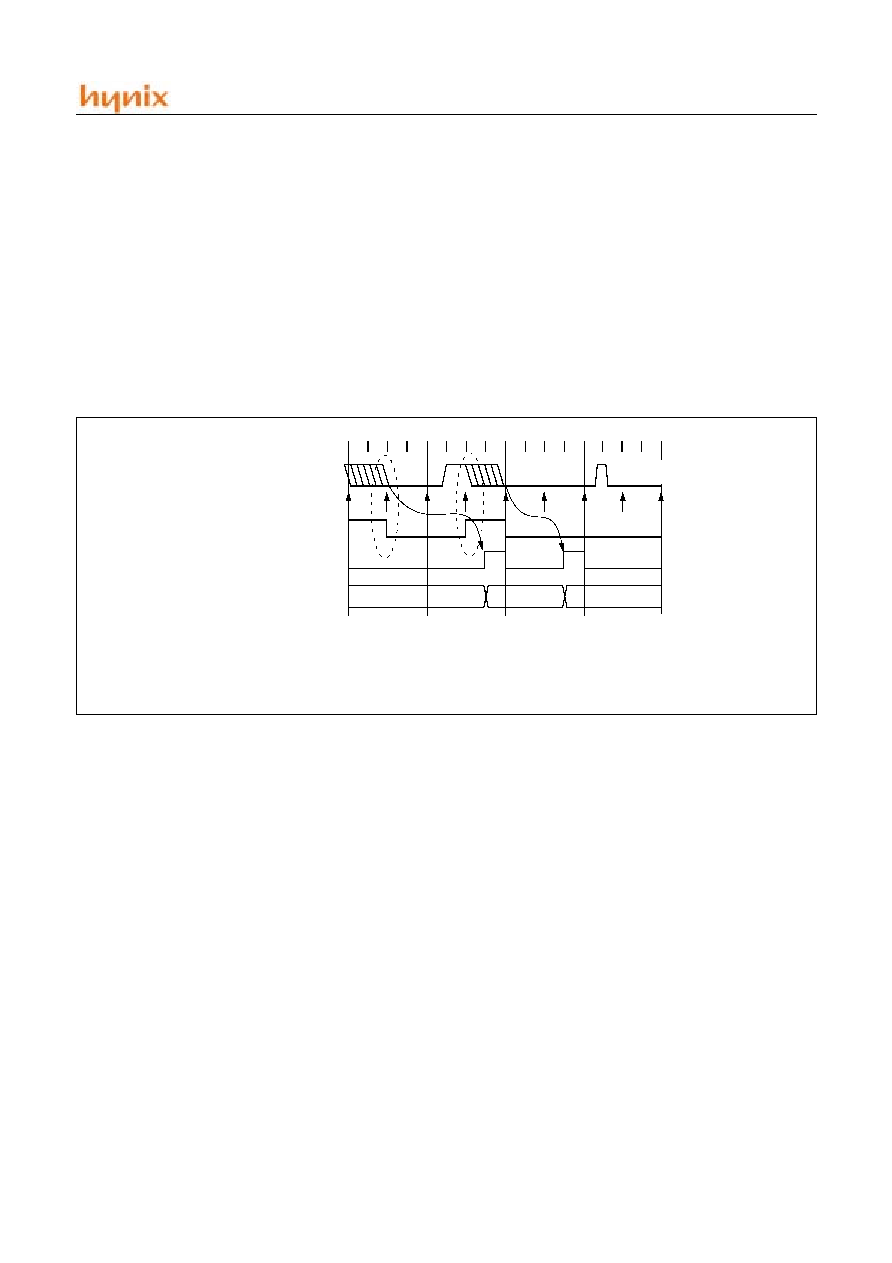
FIGURE 10-2 SUCCESSIVE I/O OPERATION
MOVWF UPIO
PC
UP5:UP0
Instruction
This example shows a write
fetched
Q1 Q2 Q3 Q4 Q1 Q2 Q3 Q4 Q1 Q2 Q3 Q4 Q1 Q2 Q3 Q4
PC+1
PC+2
PC+3
MOVF UPIO,W
NOP
NOP
Port pin
written here
Port pin
sampled here
to UPIO followed by a read
from UPIO.
Instruction
executed
MOVWF UPIO
(Write to UPIO)
MOVF UPIO,W
(Read UPIO)
NOP
Data setup time = (0.25 T
CY
-T
PD
)
where: T
CY
= instruction cycle
T
PD
= propagation delay
Therefore, at higher clock frequenies,
a write followed by a read may be
problematic.
HMS77C2000/2001
Nov. 2002 Ver 1.1
29
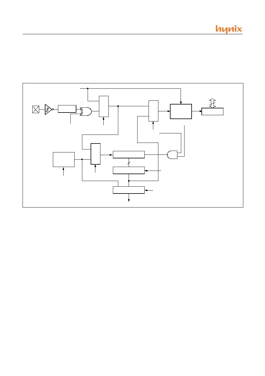
11. TIMER0 MODULE AND TMR0 REGISTER
The Timer0 module has the following features:
- 8-bit timer/counter register, TMR0
- Readable and writable
- 8-bit software programmable prescaler
- Internal
or
external clock select
- Edge select for external clock
Figure 11-1 is a simplified block diagram of the Timer0
module.
Timer mode is selected by clearing the T0CS bit (OP-
TION<5>). In timer mode, the Timer0 module will incre-
ment every instruction cycle (without prescaler). If TMR0
register is written, the increment is inhibited for the follow-
ing two instruction cycles (Figure 11-2 and Figure 11-3).
The user can work around this by writing an adjusted value
to the TMR0 register.
Counter mode is selected by setting the T0CS bit (OP-
TION<5>). In this mode, Timer0 will increment either on
every rising or falling edge of pin T0CKI. The T0SE bit
(OPTION<4>) determines the source edge. Clearing the
T0SE bit selects the rising edge. Restrictions on the exter-
nal clock input are discussed in detail in Section 6.1.
The prescaler may be used by either the Timer0 module or
the Watchdog Timer, but not both. The prescaler assign-
ment is controlled in software by the control bit PSA (OP-
TION<3>). Clearing the PSA bit will assign the prescaler
to Timer0. The prescaler is not readable or writable. When
the prescaler is assigned to the Timer0 module, prescale
values of 1:2, 1:4,..., 1:256 are selectable. Section 6.2 de-
tails the operation of the prescaler.
A summary of registers associated with the Timer0 module
is found in Table 6-1.
FIGURE 11-1 TIMER0 BLOCK DIAGRAM
F
OSC
/4
1
UP2/EC0
pin
0
Sync with
Internal
Clocks
TMR0 reg
8
Data bus
(2 T
CY
delay)
T0SE
T0CS
1
MUX
0
1
MUX
PSA
1
PS
OUT
PS
OUT
Sync
Programmable
Prescaler
3
PS2, PS1, PS0
1
Note 1 : Bits T0CS, T0SE, PSA, PS2, PS1 and PS0 are located in the OPTION register.
2 : The prescaler is shared with the watchdog timer.
Noise
Filter
HMS77C2000/2001
30
Nov. 2002 Ver 1.1
Legend: Shaded cells not used by Timer0, - = unimplemented, x = unknown, u = unchanged.
11.1 USING TIMER0 WITH AN EXTERNAL
CLOCK
When an external clock input is used for Timer0, it must
meet certain requirements. The external clock requirement
is due to internal phase clock (TOSC) synchronization. Al-
so, there is a delay in the actual incrementing of Timer0 af-
ter synchronization.
11.1.1 EXTERNAL CLOCK SYNCHRONIZATION
When no prescaler is used, the external clock input is the
same as the prescaler output. The synchronization of
T0CKI with the internal phase clocks is accomplished by
sampling the prescaler output on the Q2 and Q4 cycles of
the internal phase clocks (Figure 11-4). Therefore, it is
necessary for T0CKI to be high for at least 2TOSC (and a
small RC delay of 20 ns) and low for at least 2TOSC (and
FIGURE 11-2 TIMER0 TIMING: INTERNAL CLOCK/NO PRESCALER
FIGURE 11-3 TIMER0 TIMING: INTERNAL CLOCK/NO PRESCALER 1:2
Address
Name
Bit7
Bit6
Bit5
Bit4
Bit3
Bit2
Bit1
Bit0
Power-On
Reset
RESET and
WDT Reset
01
H
TMR0
Timer0 - 8-bit real-time clock/counter
xxxx xxxx
uuuu uuuu
N/A
OPTION
UPWU
UPPU
T0CS
T0SE
PSA
PS2
PS1
PS0
1111 1111
0011 1111
N/A
TRIS
-
-
UP5
UP4
UP3
UP2
UP1
UP0
--11 1111
--11 1111
TABLE 11-1 REGISTERS ASSOCIATED WITH TIMER0
[ W
'
TMR0 ]
PC-1
TMR0
Instruction
Fetch
Q1 Q2 Q3 Q4
PC
Q1 Q2 Q3 Q4
PC+1
Q1 Q2 Q3 Q4
PC+2
Q1 Q2 Q3 Q4
PC+3
Q1 Q2 Q3 Q4
PC+4
Q1 Q2 Q3 Q4
PC+5
Q1 Q2 Q3 Q4
PC+6
Q1 Q2 Q3 Q4
[ TMR0
'
W ]
[ TMR0
'
W ]
[ TMR0
'
W ]
[ TMR0
'
W ]
[ TMR0
'
W ]
T0
T0+1
T0+2
NT0
NT0+1
NT0+2
Write TMR0
executed
Read TMR0
reads NT0
Read TMR0
reads NT0
Read TMR0
reads NT0
Read TMR0
reads NT0+1
Read TMR0
reads NT0+2
PC
(Program
Counter)
Instruction
Executed
[ W
'
TMR0 ]
PC-1
TMR0
Instruction
Fetch
Q1 Q2 Q3 Q4
PC
Q1 Q2 Q3 Q4
PC+1
Q1 Q2 Q3 Q4
PC+2
Q1 Q2 Q3 Q4
PC+3
Q1 Q2 Q3 Q4
PC+4
Q1 Q2 Q3 Q4
PC+5
Q1 Q2 Q3 Q4
PC+6
Q1 Q2 Q3 Q4
[ TMR0
'
W ]
[ TMR0
'
W ]
[ TMR0
'
W ]
[ TMR0
'
W ]
[ TMR0
'
W ]
T0
T0+1
NT0
NT0+1
PC
(Program
Counter)
Write TMR0
executed
Read TMR0
reads NT0
Read TMR0
reads NT0
Read TMR0
reads NT0
Read TMR0
reads NT0+1
Read TMR0
reads NT0+2
Instruction
Executed
HMS77C2000/2001
Nov. 2002 Ver 1.1
31
a small RC delay of 20 ns). Refer to the electrical specifi-
cation of the desired device.
When a prescaler is used, the external clock input is divid-
ed by the asynchronous ripple counter-type prescaler so
that the prescaler output is symmetrical. For the external
clock to meet the sampling requirement, the ripple counter
must be taken into account. Therefore, it is necessary for
T0CKI to have a period of at least 4TOSC (and a small RC
delay of 40 ns) divided by the prescaler value. The only re-
quirement on T0CKI high and low time is that they do not
violate the minimum pulse width requirement of 10 ns. Re-
fer to parameters 40, 41 and 42 in the electrical specifica-
tion of the desired device.
11.1.2 TIMER0 INCREMENT DELAY
Since the prescaler output is synchronized with the internal
clocks, there is a small delay from the time the external
clock edge occurs to the time the Timer0 module is actual-
ly incremented. Figure 11-4 shows the delay from the ex-
ternal clock edge to the timer incrementing.
11.1.3 OPTION REGISTER EFFECT ON UP2 TRIS
If the option register is set to read TIMER0 from the pin,
the port is forced to an input regardless of the TRIS register
setting.
11.2 PRESCALER
An 8-bit counter is available as a prescaler for the Timer0
module, or as a postscaler for the Watchdog Timer (WDT),
respectively. For simplicity, this counter is being referred
to as "prescaler" throughout this data sheet. Note that the
prescaler may be used by either the Timer0 module or the
WDT, but not both. Thus, a prescaler assignment for the
Timer0 module means that there is no prescaler for the
WDT, and vice-versa.
The PSA and PS2:PS0 bits (OPTION<3:0>) determine
prescaler assignment and prescale ratio.
When assigned to the Timer0 module, all instructions writ-
ing to the TMR0 register (e.g.,
CLRF 1
,
MOVWF 1
,
BSF
1,x, etc.) will clear the prescaler. When assigned to WDT,
a
CLRWDT
instruction will clear the prescaler along with
the WDT. The prescaler is neither readable nor writable.
On a RESET, the prescaler contains all '0's.
11.2.1 SWITCHING PRESCALER ASSIGNMENT
The prescaler assignment is fully under software control
(i.e., it can be changed "on the fly" during program execu-
tion). To avoid an unintended device RESET, the follow-
ing instruction sequence (Example 6-1) must be executed
when changing the prescaler assignment from Timer0 to
the WDT.
EXAMPLE 6-1: CHANGING PRESCALER
(TIMER0
WDT)
1.CLRWDT ;Clear
WDT
2.CLRF TMR0
;Clear TMR0 & Prescaler
3.MOVLW `00xx1111'b ;These 3 lines (5,6,7)
4.OPTION
; are required only if
; desired
5.CLRWDT
;PS<2:0> are 000 or 001
6.MOVLW `00xx1xxx'b ;Set Postscaler to
7.OPTION
; desired WDT rate
To change prescaler from the WDT to the Timer0 module,
use the sequence shown in Example 6-2. This sequence
must be used even if the WDT is disabled. A
CLRWDT
in-
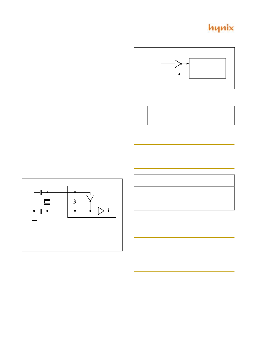
FIGURE 11-4 TIMER0 TIMING WITH EXTERNAL CLOCK
Q1 Q2 Q3 Q4 Q1 Q2 Q3 Q4 Q1 Q2 Q3 Q4
T0
T0+1
Note 1: Delay from clock input change to TMR0 increment is 3T
OSC
to 7T
OSC
. (Duration of Q = T
OSC
).
Q1 Q2 Q3 Q4
T0+2
External Clock Input or
Prescaler Output
(2)
External Clock/Prescaler
Output After Sampling
Increment TMR0 (Q4)
TMR0
Small Pulse
misses sampling
(1)
(3)
Therefore, the error in measuring the interval between two edges on TMR0 input =
�
4T
OSC
max.
2: External clock if no prescaler selected, prescaler output otherwise.
3: The arrows indicate the points in time where sampling occurs.
HMS77C2000/2001
32
Nov. 2002 Ver 1.1
struction should be executed before switching the prescal-
er.
EXAMPLE 6-2: CHANGING PRESCALER
(WDT
TIMER0)
CLRWDT
;Clear WDT and
;prescaler
MOVLW `xxxx0xxx' ;Select TMR0, new
;prescale value and
;clock source
OPTION
FIGURE 11-5 BLOCK DIAGRAM OF THE TIMER0/WDT PRESCALER
T
CY
( = F
OSC
/4)
1
8-bit Prescaler
UP2/EC0
pin
0
Sync with
Internal
Clocks
TMR0 reg
8
Data bus
(2cycle delay)
T0SE
8
T0CS
MUX
0
1
MUX
1
0
PSA
MUX
8 - to - 1 MUX
Watchdog
Timer
MUX
PS2:PS0
PSA
PSA
1
0
WDT Time-Out
WDT Enable bit
clear
Noise
Filter

HMS77C2000/2001
Nov. 2002 Ver 1.1
33
12. SPECIAL FEATURES OF THE CPU
What sets a microcontroller apart from other processors
are special circuits to deal with the needs of real-time ap-
plications. The HMS77C2000 and HMS77C2001 have a
host of such features intended to maximize system reliabil-
ity, minimize cost through elimination of external compo-
nents, provide power saving operating modes and offer
code protection.
These features are:
- Oscillator
selection
- Reset
- Power-On Reset (POR)
- Internal Reset Timer (IRT)
- Wake-up from SLEEP on pin change
- Watchdog Timer (WDT)
- SLEEP
- Code
protection
- ID
locations
- In-circuit Serial Programming
The HMS77C2000 and HMS77C2001 have a Watchdog
Timer which can be shut off only through configuration bit
WDTE. It runs off of its own RC oscillator for added reli-
ability. If using XT or LF selectable oscillator options,
there is always an 18 ms (nominal) delay provided by the
Internal
Reset Timer (IRT), intended to keep the chip in
reset until the crystal oscillator is stable. If using IRC or
ERC there is an 18 ms delay only on V
DD
power-up.
With this timer on-chip, most applications need no external
reset circuitry.
The SLEEP mode is designed to offer a very low current
power-down mode. The user can wake-up from SLEEP
through a change on input pins or through a Watchdog
Timer time-out. Several oscillator options are also made
available to allow the part to fit the application, including
an internal 4 MHz oscillator.
The ERC oscillator option saves system cost while the LF
crystal option saves power. A set of configuration bits are
used to select various options.
12.1 CONFIGURATION BITS
The HMS77C2000 and HMS77C2001 configuration word
consists of 12 bits. Configuration bits can be programmed
to select various device configurations. Two bits are for the
selection of the oscillator type, one bit is the Watchdog
Timer enable bit, and one bit is the RESET enable bit.
FIGURE 12-1 CONFIGURATION WORD FOR HMS77C2000/1
bit11
bit0
4
3
2
1
PORLS: Power on reset level selection bit
1 = 1.7v(Typ.)
0 = Data retention voltage 0.6v(Typ.)
RESETE: RESET pin enable bit.
1 = RESET pin enabled
0 = RESET tied to
V
DD
(internally).
CP: Code protection bit.
1 = Code protection off
0 = Code protection on
WDTE: Watchdog timer enable bit
1 = WDT enabled
0 = WDT disabled
FOSC1~FOSC0: Oscillator selection bits
11 = ERC - external RC oscillator
10 = IRC - internal RC oscillator
01 = XT oscillator
00 = LF oscillator
Address
: FFF
H
CP
WDTE FOSC1 FOSC0
-
Unimplemented, read as `0'
Configuration Word
RESETE
PORLS
5
HMS77C2000/2001
34
Nov. 2002 Ver 1.1
12.2 OSCILLATOR CONFIGURATIONS
12.2.1 OSCILLATOR TYPES
The HMS77C2000 and HMS77C2001 can be operated in
four different oscillator modes. The user can program two
configuration bits (FOSC1:FOSC0) to select one of these
four modes:
- LF:
Low
Frequency
- XT:
Crystal/resonator
- IRC: Internal 4 MHz Oscillator
- ERC:
External
Resistor/Capacitor
12.2.2 CRYSTAL OSCILLATOR / CERAMIC RESO-
NATORS
In XT or LF modes, a crystal or ceramic resonator is con-
nected to the UP5/X
IN
and UP4/X
OUT
pins to establish os-
cillation (Figure 12-2). The HMS77C2000 and
HMS77C2001 oscillator design requires the use of a paral-
lel cut crystal. Use of a series cut crystal may give a fre-
quency out of the crystal manufacturers specifications.
When in XT or LF modes, the device can have an external
clock source drive the UP5/X
IN
pin (Figure 12-3).
Note: These values are for design guidance only. Since
each resonator has its own characteristics, the user
should consult the resonator manufacturer for ap-
propriate values of external components.
Note: These values are for design guidance only. Rs may
be required to avoid overdriving crystals with low
drive level specification. Since each crystal has its
own characteristics, the user should consult the
crystal manufacturer for appropriate values of exter-
nal components.
12.2.3 EXTERNAL RC OSCILLATOR
For timing insensitive applications, the RC device option
offers additional cost savings. The RC oscillator frequency
is a function of the supply voltage, the resistor (Rext) and
capacitor (Cext) values, and the operating temperature. In
addition to this, the oscillator frequency will vary from unit
to unit due to normal process parameter variation. Further-
more, the difference in lead frame capacitance between
FIGURE 12-2 CRYSTAL OPERATION OR CERAMIC
RESONATOR (XT OR LF OSC
CONFIGURATION)
X
IN
X
OUT
To internal
RF
(2)
SLEEP
logic
XTAL
C2
1
C1
1
Note 1: See Capacitor Selection tables for recommended
values of C1 and C2.
2: RF varies with the crystal chosen
(approx. value = 10 M
).
FIGURE 12-3 EXTERNAL CLOCK INPUT OPERATION
(XT OR LF OSC CONFIGURATION)
Osc
Type
Resonator
Freq
Cap.Range
C1
Cap. Range
C2
XT
4.0 MHz
30 pF
30 pF
TABLE 12-1 CAPACITOR SELECTION FOR CERAMIC
RESONATORS
Osc
Type
Crystal
Freq
Cap.Range
C1
Cap. Range
C2
LF
32 kHz
1
1.
For V
DD
> 4.5V, C1 = C2
30 pF is recommended.
15 pF
15 pF
XT
200 kHz
1 MHz
4 MHz
47~68 pF
15 pF
15 pF
47-68 pF
15 pF
15 pF
TABLE 12-2 CAPACITOR SELECTION FOR CRYSTAL
OSCILLATOR
X
OUT
X
IN
OPEN
Clock from
ext. system

HMS77C2000/2001
Nov. 2002 Ver 1.1
35
package types will also affect the oscillation frequency, es-
pecially for low Cext values. The user also needs to take
into account variation due to tolerance of external R and C
components used.
Figure 12-4 shows how the R/C combination is connected
to the HMS77C2000 and HMS77C2001. For Rext values
below 2.2 k
, the oscillator operation may become unsta-
ble, or stop completely. For very high Rext values e.g., 1
M
) the oscillator becomes sensitive to noise, humidity
and leakage. Thus, we recommend keeping Rext between
3 k
and 100 k
.
Although the oscillator will operate with no external ca-
pacitor (Cext = 0 pF), we recommend using values above
20 pF for noise and stability reasons. With no or small ex-
ternal capacitance, the oscillation frequency can vary dra-
matically due to changes in external capacitances, such as
PCB trace capacitance or package lead frame capacitance.
The Electrical Specifications sections show RC frequency
variation from part to part due to normal process variation.
The variation is larger for larger R (since leakage current
variation will affect RC frequency more for large R) and
for smaller C (since variation of input capacitance will af-
fect RC frequency more).
Also, see the Electrical Specifications sections for varia-
tion of oscillator frequency due to V
DD
for given Rext/
Cext values as well as frequency variation due to operating
temperature for given R, C, and V
DD
values.
12.2.4 INTERNAL 4 MHz RC OSCILLATOR
The internal RC oscillator provides a fixed 4 MHz (nomi-
nal) system clock at V
DD
= 5V and 25
�
C, see "Electrical
Characteristics" section for information on variation over
voltage and temperature.
In addition, a calibration instruction is programmed into
the top of memory which contains the calibration value for
the internal RC oscillator. This location is never code pro-
tected regardless of the code protect settings. This value is
programmed as a
MOVLW
XX
instruction where xx is the
calibration value, and is placed at the reset vector. This will
load the W and OSCCAL registers with the calibration val-
ue upon reset and the PC will then roll over to the users
program at address 000
H
. And the user has to consider the
bits related to power fail detection circuit.
If the user then want to update the calibration value, has to
rewrite the OSCCAL register with the user's settig value.
OSCCAL, when written to with the calibration value, will
"trim" the internal oscillator to remove process variation
from the oscillator frequency.
Note: Please note that erasing the device will also erase
the pre-programmed internal calibration value for
the internal oscillator. The calibration value must be
read prior to erasing the part. so it can be repro-
grammed correctly later.
Bits <7:3>, CAL4-CAL0 are used for calibration. Adjust-
ing CAL4~0 from 00000 to 11111 yields a higher clock
speed.
12.3 RESET
The device differentiates between various kinds of reset:
- Power on reset (POR)
- RESET reset during normal operation
- RESET reset during SLEEP
- WDT time-out reset during normal operation
- WDT time-out reset during SLEEP
- Wake-up from SLEEP on pin change
Some registers are not reset in any way; they are unknown
on POR and unchanged in any other reset. Most other reg-
isters are reset to "reset state" on power-on reset (POR),
RESET, WDT or wake-up on pin change reset during nor-
mal operation. They are not affected by a WDT reset dur-
ing SLEEP or RESET reset during SLEEP, since these
resets are viewed as resumption of normal operation. The
exceptions to this are TO, PD, and UPWUF bits. They are
set or cleared differently in different reset situations. These
bits are used in software to determine the nature of reset.
See Table 8-3 for a full description of reset states of all reg-
FIGURE 12-4 EXTERNAL RC OSCILLATOR MODE
N
R
ext
Internal
V
DD
X
IN
Clock
C
ext
V
SS
HMS77C2000/2001
36
Nov. 2002 Ver 1.1
isters.
Legend: - = unimplemented, read as `0', x = unknown, u = unchanged. q = value depends on condition.
Legend : - = unimplemented, read as `0', x = unknown, u = unchanged.
12.3.1 RESET ENABLE
This configuration bit when unprogrammed (left in the `1'
state) enables the external RESET function. When pro-
grammed, the RESET function is tied to the internal V
DD
,
and the pin is assigned to be a UPIO. See Figure 12-5.
When pin UP3/RESET/V
PP
is configured as RESET, the
Register
Address
Power-On Reset
RESET Reset
WDT time-out
Wake-up on Pin Change
W
N/A
qqqq xxxx
1
qqqq uuuu
INDF
00
H
xxxx xxxx
uuuu uuuu
TMR0
01
H
xxxx xxxx
uuuu uuuu
PC
02
H
1111 1111
1111 1111
STATUS
03
H
0001 1xxx
q00q quuu
2
FSR(HMS77C2000)
04
H
111x xxxx
111u uuuu
FSR(HMS77C2001)
04
H
110x xxxx
11uu uuuu
OSCCAL
05
H
1000 0000
uuuu uuu0
UPIO
06
H
--xx xxxx
--uu uuuu
OPTION
N/A
1111 1111
1111 1111
TRIS
N/A
--11 1111
--11 1111
TABLE 12-3 RESET CONDITIONS FOR ALL REGISTERS
1. Bits <7;2> of W register contain oscillator calibration values due to
MOVLW XX
instruction at top of memory.
2. See Table 12-7 for reset value for specific conditions.
If reset was due to wake-up on pin change, then bit7 = 1. All other resets will cause bit 7 = 0.
STATUS (Addr:03
H
)
PCL (Addr:02
H
)
Power On reset
0001 1xxx
1111 1111
RESET reset during normal operation
000u uuuu
1111 1111
RESET reset during SLEEP
0001 0uuu
1111 1111
WDT reset during SLEEP
0000 0uuu
1111 1111
WDT reset normal operation
0000 uuuu
1111 1111
Wake-up from SLEEP on pin change
1001 0uuu
1111 1111
TABLE 12-4 RESET CONDITIONS FOR SPECIAL REGISTER
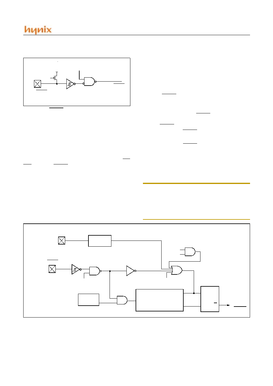
HMS77C2000/2001
Nov. 2002 Ver 1.1
37
internal pull-up is always on.
12.4 POWER-ON RESET (POR)
The HMS77C2000 and HMS77C2001 incorporate on-chip
Power-On Reset (POR) circuitry which provides an inter-
nal chip reset for most power-up situations.
The on-chip POR circuit holds the chip in reset until V
DD
has reached a high enough level for proper operation. To
take advantage of the internal POR, program the UP3/RE-
SET/V
PP
pin as RESET and tie through a resistor to V
DD
or program the pin as UP3. An internal weak pull-up resis-
tor is implemented using a transistor. This will eliminate
external RC components usually needed to create a Power-
on Reset. A maximum rise time for V
DD
is specified. See
`Electrical Characteristics' for details.
When the device starts normal operation (exits the reset
condition), device operating parameters (voltage, frequen-
cy, temperature, ...) must be met to ensure operation. If
these conditions are not met, the device must be held in re-
set until the operating parameters are met.
A simplified block diagram of the on-chip power-on reset
circuit is shown in Figure 12-6.
The power-on reset circuit and the internal reset timer cir-
cuit are closely related. On power-up, the reset latch is set
and the IRT is reset. The IRT timer begins counting once
it detects RESET to be high. After the time-out period,
which is typically 18 ms, it will reset the reset latch and
thus end the onchip reset signal.
A power-up example where RESET is held low is shown
in Figure 12-7. V
DD
is allowed to rise and stabilize before
bringing RESET high. The chip will actually come out of
reset T
IRT
msec after RESET goes high.
In Figure 12-8 and Figure 12-9, the on-chip power-on reset
feature is being used (RESET and V
DD
are tied together or
the pin is programmed to be UP3.). The V
DD
is stable be-
fore the start-up timer times out and there is no problem in
getting a proper reset.
And the user can select the level of power-on reset (0.6V,
1.7V).
Note: When the device starts normal operation (exits the
reset condition), device operating parameters (volt-
age, frequency, temperature, etc.) must be meet to
ensure operation. If these conditions are not met,
the device must be held in reset until the operating
conditions are met.
FIGURE 12-5 RESET SELECT
INTERNAL RESET
RESETE
WEAK
PULL-UP
UP3/RESET/V
PP
FIGURE 12-6 SIMPLIFIED BLOCK DIAGRAM OF ON-CHIP RESET CIRCUIT
V
DD
Internal RESET
Power-Up
Detect
UP3/RESET/V
PP
pin
On-Chip
IRT OSC
reset
8-bit asynch ripple counter
(start-up timer)
S
R
Q
Q
wake-up on
pin change
pin change
SLEEP
RESETE
WDT time out
HMS77C2000/2001
38
Nov. 2002 Ver 1.1
FIGURE 12-7 TIME-OUT SEQUENCE ON POWER-UP(RESET PULLED LOW)
V
DD
RESET
INTERNAL POR
IRT TIMER-OUT
INTERNAL RESET
T
IRT
FIGURE 12-8 TIME-OUT SEQUENCE ON POWER-UP(RESET TIED TO V
DD
): FAST V
DD
RISE TIME
V
DD
RESET
INTERNAL POR
IRT TIMER-OUT
INTERNAL RESET
T
IRT
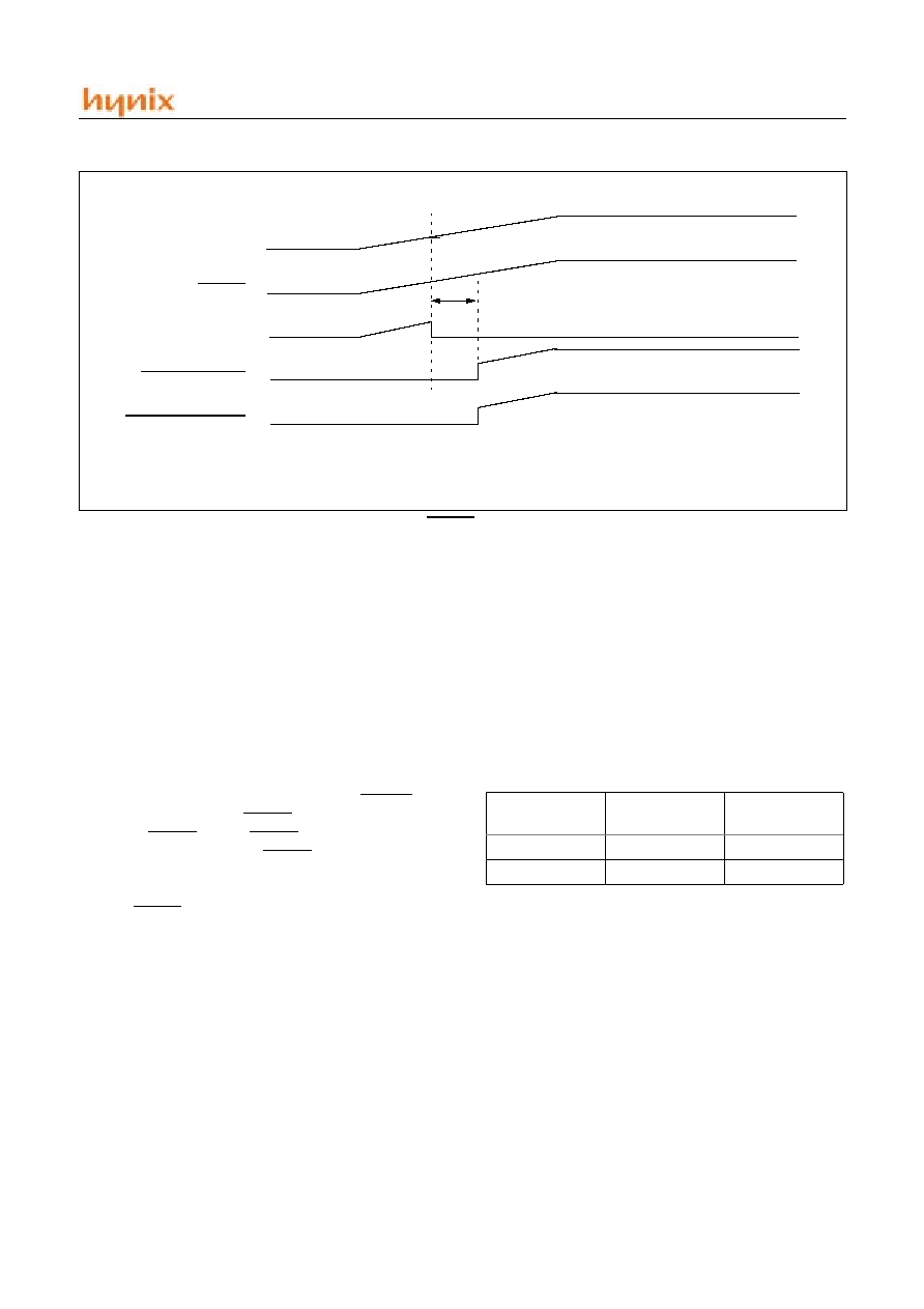
HMS77C2000/2001
Nov. 2002 Ver 1.1
39
12.5 INTERNAL RESET TIMER (IRT)
In the HMS77C2000 and HMS77C2001, IRT runs from
RESET and varies based on oscillator selection (see Table
8-5.)
The IRT operates on an internal RC oscillator. The proces-
sor is kept in RESET as long as the IRT is active. The IRT
delay allows V
DD
to rise above V
DD
min., and for the os-
cillator to stabilize.
Oscillator circuits based on crystals or ceramic resonators
require a certain time after power-up to establish a stable
oscillation. The on-chip IRT keeps the device in a RESET
condition for approximately 18ms after RESET has
reached a logic high (V
IH
RESET) level. Thus, program-
ming UP3/RESET/V
PP
as RESET and using an external
RC network connected to the RESET input is not required
in most cases, allowing for savings in cost-sensitive and/or
space restricted applications, as well as allowing the use of
the UP3/RESET/V
PP
pin as a general purpose input.
The Device Reset time delay will vary from chip to chip
due to V
DD
, temperature, and process variation. See AC
parameters for details.
The IRT will also be triggered upon a Watchdog Timer
time-out. This is particularly important for applications us-
ing the WDT to wake from SLEEP mode automatically.
12.6 WATCHDOG TIMER (WDT)
The Watchdog Timer (WDT) is a free running on-chip RC
oscillator which does not require any external components.
This RC oscillator is separate from the external RC oscil-
lator of the UP5/X
IN
pin and the internal 4 MHz oscillator.
That means that the WDT will run even if the main proces-
sor clock has been stopped, for example, by execution of a
SLEEP
instruction. During normal operation or SLEEP, a
WDT reset or wake-up reset generates a device RESET.
The TO bit (STATUS<4>) will be cleared upon a Watch-
dog Timer reset. The WDT can be permanently disabled
by programming the configuration bit WDTE as a `0' (Sec-
tion 8.1). Refer to the HMS77C2000 and HMS77C2001
Programming Specifications to determine how to access
the configuration word.
12.6.1 WDT PERIOD
The WDT has a nominal time-out period of 18 ms, (with
no prescaler). If a longer time-out period is desired, a pres-
caler with a division ratio of up to 1:128 can be assigned to
the WDT (under software control) by writing to the OP-
TION register. Thus, a time-out period of a nominal 2.3
seconds can be realized. These periods vary with tempera-
ture, V
DD
and part-to-part process variations (see DC
specs).
Under worst case conditions (V
DD
= Min., Temperature =
Max., max. WDT prescaler), it may take several seconds
FIGURE 12-9 TIME-OUT SEQUENCE ON POWER-UP(RESET TIED TO V
DD
): SLOW V
DD
RISE TIME
V
DD
RESET
INTERNAL POR
IRT TIMER-OUT
INTERNAL RESET
T
IRT
Oscillator
Configuration
POR Reset
Subsequent
Resets
IRC & ERC
18 ms(typ.)
300us(typ.)
XT & LF
18 ms(typ.)
18ms(typ.)
TABLE 12-5 IRT(INTERNAL RESET TIMER PERIOD)
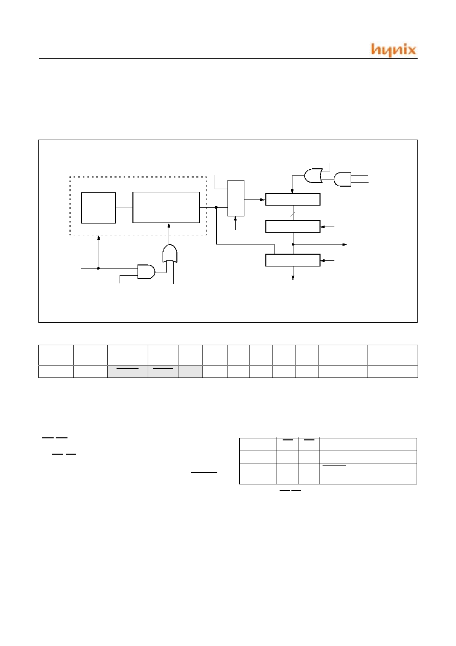
HMS77C2000/2001
40
Nov. 2002 Ver 1.1
before a WDT time-out occurs.
12.6.2 WDT PROGRAMMING CONSIDERATIONS
The
CLRWDT
instruction clears the WDT and the postscal-
er, if assigned to the WDT, and prevents it from timing out
and generating a device RESET.
The
SLEEP
instruction resets the WDT and the postscaler,
if assigned to the WDT. This gives the maximum SLEEP
time before a WDT wake-up reset.
Legend: Shaded boxes = Not used by WDT, - = unimplemented, read as `0', u = unchanged.
12.7 TIME-OUT SEQUENCE, POWER DOWN,
AND WAKE-UP FROM SLEEP STATUS BITS
(TO/PD/UPWUF)
The TO, PD, and UPWUF bits in the STATUS register can
be tested to determine if a RESET condition has been
caused by a power-up , powe fail condition, a RESET,
Watchdog Timer (WDT) reset or SLEEP mode wake-up
reset.
FIGURE 12-10 WATCHDOG TIMER BLOCK DIAGRAM
Address
Name
Bit7
Bit6
Bit5
Bit4
Bit3
Bit2
Bit1
Bit0
Power-On
Reset
All other
resets
N/A
OPTION
GPWU
GPPU
T0CS T0SE
PSA
PS2
PS1
PS0
1111 1111
1111 1111
TABLE 12-6 SUMMARY OF REGISTERS ASSOCIATED WITH THE WATCHDOG TIMER
Postscaler
8
1
0
PSA
MUX
8 - to - 1 MUX
8-bit asynchronous
ripple counter
MUX
PS2:PS0
PSA
1
0
WDT Time-Out
To TMR0
From TMR0 Clock Source
clear
on-chip
RC-OSC
Watchdog Timer
enable
WDTE
SLEEP
clearing WDT
SLEEP
clearing WDT
PSA
UPWUF
TO
PD
RESET was caused by
0
1
1
Power-up (POR)
0
u
u
RESET or PFD reset from
normal operation
TABLE 12-7 TO/PD/UPWUF STATUS AFTER RESET
Legend: u = unchanged
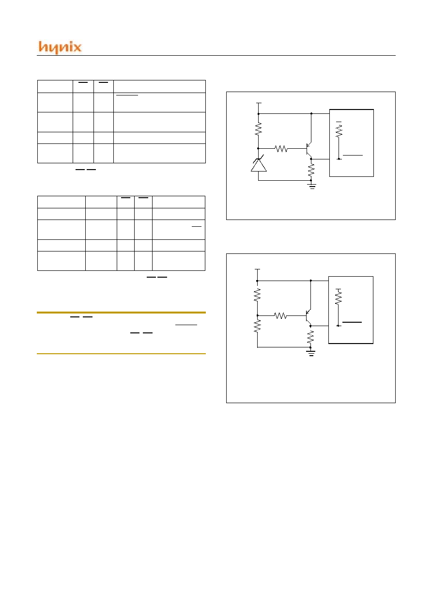
HMS77C2000/2001
Nov. 2002 Ver 1.1
41
Note: The TO, PD, and UPWUF bits maintain their status
(u) until a reset occurs. A lowpulse on the RESET in-
put does not change the TO, PD, and UPWUF sta-
tus bits.
12.8 RESET ON BROWN-OUT
A brown-out is a condition where device power (V
DD
) dips
below its minimum value, but not to zero, and then recov-
ers. The device should be reset in the event of a brown-out.
To reset HMS77C2000 and HMS77C2001 when a brown-
out occurs, external brown-out protection circuits may be
built, as shown in Figure 12-11, Figure 12-12.
12.9 POWER-DOWN MODE (SLEEP)
A device may be powered down (SLEEP) and later pow-
ered up (Wake-up from SLEEP).
12.9.1 SLEEP
The Power-Down mode is entered by executing a SLEEP
instruction.
If enabled, the Watchdog Timer will be cleared but keeps
running, the TO bit (STATUS<4>) is set, the PD bit (STA-
TUS<3>) is cleared and the oscillator driver is turned off.
The I/O ports maintain the status they had before the
SLEEP
instruction was executed (driving high, driving
0
1
0
RESET Wake-up from
SLEEP
0
0
u
WDT time-out from normal
operation
0
0
0
WDT wake-up from SLEEP
1
1
0
Wake-up from SLEEP on pin
change
Event
UPWUF
TO
PD
Remarks
Power-up
0
1
1
WDT Time-
out
0
0
u
No effect on PD
SLEEP inst.
0
1
0
CLRWDT inst.
u
1
1
No effect on
UPUWF
TABLE 12-8 EFFECTS AFFECTION TO/PD/UPWUF
STATUS
Legend: u = unchanged
UPWUF
TO
PD
RESET was caused by
TABLE 12-7 TO/PD/UPWUF STATUS AFTER RESET
Legend: u = unchanged
FIGURE 12-11 BROWN-OUT PROTECTION CIRCUIT 1
FIGURE 12-12 BROWN-OUT PROTECTION CIRCUIT 2
33k
V
DD
10k
V
SS
Q1
40k
1
V
DD
RESET
This circuit will activate reset when V
DD
goes below
V
Z
+ 0.7V (wher V
Z
=Zener voltage).
V
DD
R1
V
DD
10k
V
SS
Q1
40k
1
V
DD
RESET
This brown-out circuit is less expensive, although
less accurate. Transistor Q1 turns off when V
DD
R2
V
DD
is below a certain level such that:
V
DD
= R1/(R1+R2) = 0.7V

HMS77C2000/2001
42
Nov. 2002 Ver 1.1
low, or hi-impedance).
It should be noted that a RESET generated by a WDT time-
out does not drive the RESET pin low.
For lowest current consumption while powered down, the
T0CKI input should be at V
DD
or V
SS
and the UP3/RE-
SET/V
PP
pin must be at a logic high level (V
IHMC
) if RE-
SET is enabled.
12.9.2 WAKE-UP FROM SLEEP
The device can wake-up from SLEEP through one of the
following events:
- An external reset input on UP3/RESET/V
PP
pin,
when configured as RESET.
- A Watchdog Timer time-out reset (if WDT was
enabled).
- A change on input pin UP0, UP1, or UP3/RE-
SET/V
PP
when wake-up on change is enabled.
These events cause a device reset. The TO, PD, and UP-
WUF bits can be used to determine the cause of device re-
set. The TO bit is cleared if a WDT time-out occurred (and
caused wake-up). The PD bit, which is set on power-up, is
cleared when SLEEP is invoked. The UPWUF bit indi-
cates a change in state while in SLEEP at pins UP0, UP1,
or UP3 (since the last time there was a file or bit operation
on UP port).
Note: Right before entering SLEEP, read the input pins.
When in SLEEP, wake up occurs when the values
at the pins change from the state they were in at the
last reading. If a wake-up on change occurs and the
pins are not read before reentering SLEEP, a wake
up will occur immediately even if no pins change
while in SLEEP mode.
The WDT is cleared when the device wakes from sleep, re-
gardless of the wake-up source.
12.10 PROGRAM VERIFICATION/CODE PRO-
TECTION
If the code protection bit has not been programmed, the on-
chip program memory can be read out for verification pur-
poses.
The first 64 locations can be read by the HMS77C2000 and
HMS77C2001 regardless of the code protection bit setting.
The last memory location cannot be read if code protection
is enabled on the HMS77C2000 and HMS77C2001.
12.11 ID LOCATIONS
Four memory locations are designated as ID locations
where the user can store checksum or other code identifi-
cation numbers. These locations are not accessible during
normal execution but are readable and writable during pro-
gram/verify.
Use only the lower 4 bits of the ID locations and always
program the upper 8 bits as `0's.
12.12 POWER FAIL DETECTION PROCES-
SOR
The HMS77C2000 and HMS77C2001 have an on-chip
power fail detection circuitry to immunize against power
noise. If V
DD
falls below a level for longer 100ns, the pow-
er fail detection processor may reset MCU to protect the
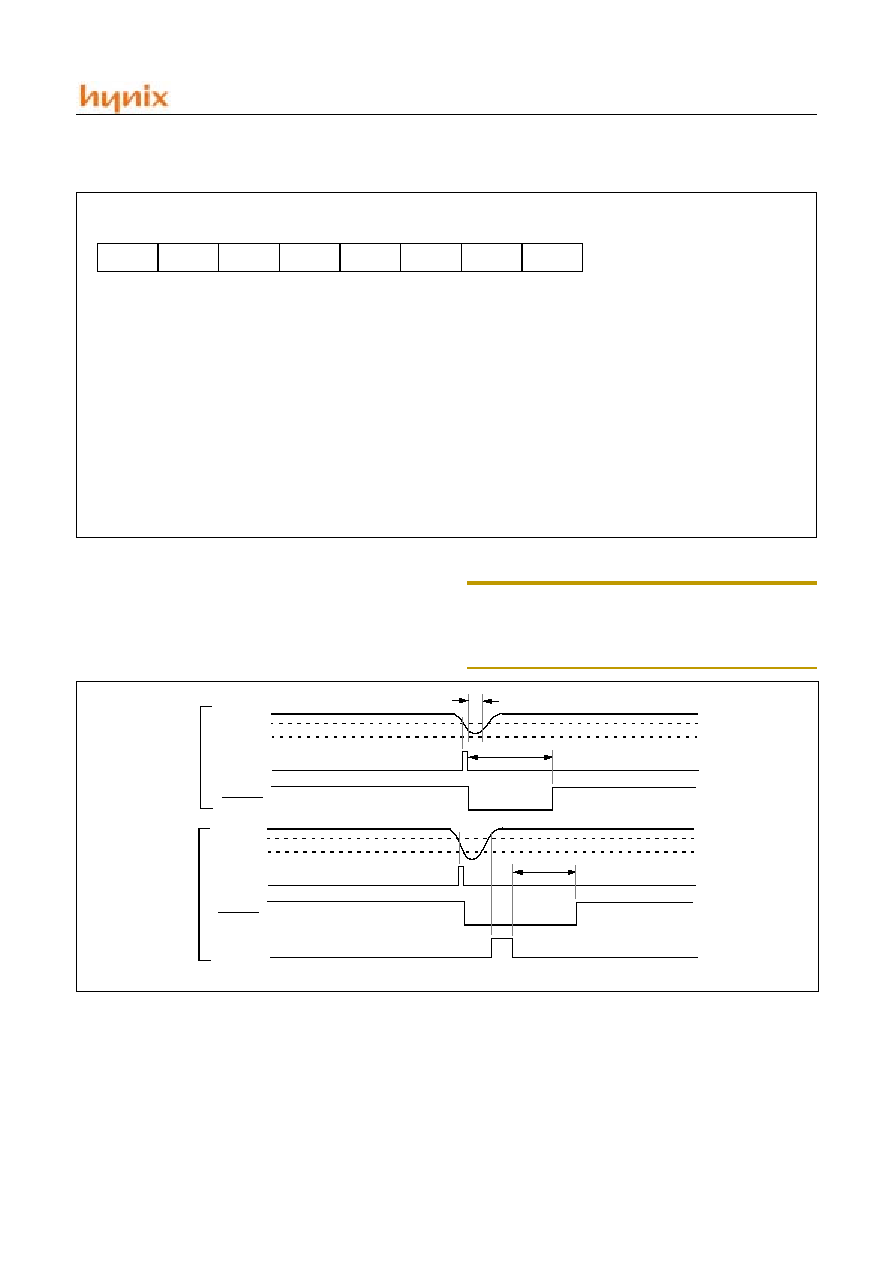
HMS77C2000/2001
Nov. 2002 Ver 1.1
43
device from the malfunction due to Power Noise.
The bit0(PFDEN) of OSCCAL register activates the PFD
Circuit, and bit1(PFDF) indicates `power fail detection sit-
uation". The normal detection level is typically 2.7V. Fig-
ure 12-14 shows a "power fail detection situations".
Note: The PFD circuit is not implemented on the in circuit
emulator, user can not experiment with it. There
fore, after final development user program, this
function may be experimented on OTP.
12.13 IN-CIRCUIT SERIAL PROGRAMMING
The HMS77C2000 and HMS77C2001 microcontrollers
with EPROM program memory can be serially pro-
grammed while in the end application circuit. This is sim-
ply done with two lines for clock and data, and three other
lines for power, ground, and the programming voltage.
This allows customers to manufacture boards with unpro-
grammed devices, and then program the microcontroller
just before shipping the product. This also allows the most
FIGURE 12-13 OSCCAL REGISTER
CAL4
R/W
CAL3
R/W
CAL2
R/W
CAL1
R/W
CAL0
R/W
-
R/W
PFDF
R/W
PFDEN
R/W
bit7
6
bit0
5
4
3
2
1
CAL4~CAL0: Calibration Bits
11111 = High frequency
10000 = Middle frequency
00000 = Low frequency
PFDF: Power-fail detection flag bit.
1 = Reset caused by PFD reset.
0 = PFD reset is not generated.
PFDEN: Power-fail detection enable bit
1 = Enable PFD
0 = Disable PFD
R = Readable bit
W = Writable bit
ADDRESS ; 05
H
RESET VALUE : 1000_0000
FIGURE 12-14 POWER FAIL DETECTION SITUATIONS
Internal
RESET
V
DD
V
DD
=2.7V
V
DR
T
NVDD
100nS
PFDEN = 1
PFDR
T
IRT
Internal
RESET
V
DD
V
DD
=2.7V
V
DR
PFDR
T
IRT
POR
PFDEN = 1
V
DD
V
DR
When V
DD
falls below approximately 0.6V or 1.7V level, Power-On Reset may occur.
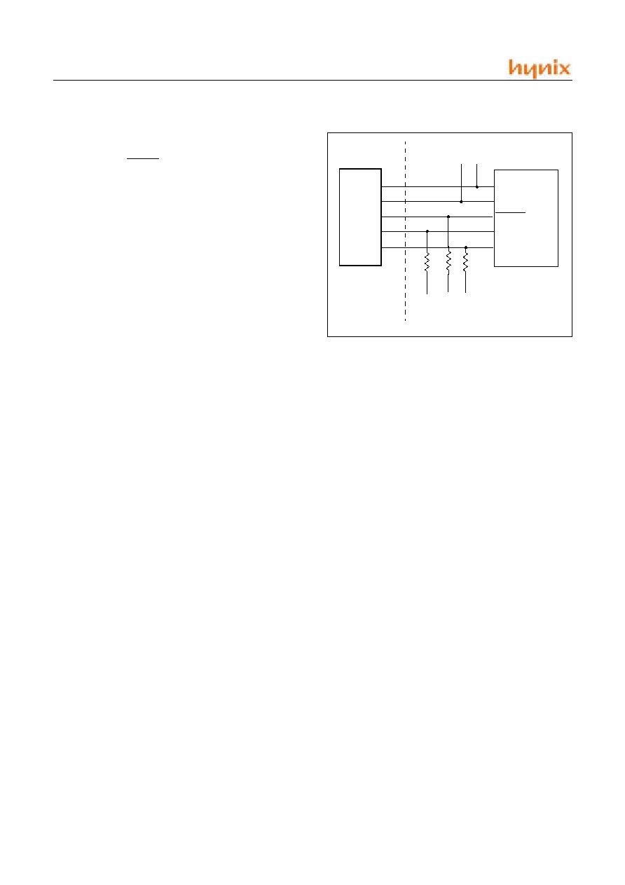
HMS77C2000/2001
44
Nov. 2002 Ver 1.1
recent firmware or a custom firmware to be programmed.
The device is placed into a program/verify mode by hold-
ing the UP0, UP1 and the other pins(UP2, UP4, UP5) low
while raising the RESET (V
PP
) pin from V
IL
to V
IH
. UP1
becomes the programming clock and UP0 becomes the
programming data. Both UP1 and UP0 are schmitt trigger
inputs in this mode.
After reset, a 6-bit command is then supplied to the device.
Depending on the command, 14-bits of program data are
then supplied to or from the device, depending if the com-
mand was a load or a read. For complete details of serial
programming, please refer to the HMS77C2000 and
HMS77C2001 programming specifications.
A typical in-circuit serial programming connection is
shown in Figure 12-15.
FIGURE 12-15 TYPICAL IN-CIRCUIT SERIAL
PROGRAMMING CONNECTION
V
DD
RESET/V
PP
V
SS
UP1
UP0
+5V
0V
V
PP
CLK
Data I/O
To Normal
Connections
To Normal
Connections
External
connector
signals

HMS77C2000/2001
Nov. 2002 Ver 1.1
45
13. IN-CIRCUIT SERIAL PROGRAMMING(ICSP) SPECIFICATIONS
13.1 PROGRAMMING THE HMS77C200X
The HMS77C2000 and HMS77C2001 can be programmed
using a serial method. Due to this serial programming, the
HMS77C2000 and HMS77C2001 can be programmed
while in the user's system increasing design flexibility.
This programming specification applies to the
HMS77C2000 and HMS77C2001 devices in all packages.
13.1.1 Hardware Requirement
The HMS77C2000 and HMS77C2001 require two pro-
grammable power supplies, one for V
DD
(4.5V to 5.5V rec-
ommended) and one for V
PP
(11.25V to 11.75V).
Both supplies should have a minimum resolution of 0.25V.
13.1.2 Programming Mode
The programming mode for the HMS77C2000 and
HMS77C2001 allows programming of user program mem-
ory, special locations used for ID, and the configuration
word for the HMS77C2000 and HMS77C2001.
13.2 PROGRAM MODE ENTRY
The program/verify mode is entered by holding UP0, UP1
and the other pins(UP2, UP4, UP5) low while raising V
PP
pin from V
IL
to V
IHH
.
Once in this mode the user program memory and the test
program memory can be accessed and programmed in a se-
rial fashion. The first selected memory location is the con-
figuration word.
Incrementing the PC once (using the increment address
command) selects location 0x000 of the regular program
memory. Afterwards all other memory locations from
001
H
~1FF
H
(HMS77C2000), 001
H
~3FF
H
(HMS77C2001)
can be addressed by incrementing the PC.
If the program counter has reached the last user program
location and is incremented again, the on-chip special
EPROM area will be addressed.
(See Figure 13-2 to determine where the special EPROM
area is located)
13.2.1 Programming Method
The programming technique is described in the following
section. It is designed to guarantee good programming
margins. It does, however, require a variable power supply
for V
DD
.
Programming Method Details
- Perform blank check at V
DD
= V
DDMIN
. Report
failure.
The device may not be properly erased.
- Program location with pulses and verify after
each pulse at V
DD
= V
DDP
:
where V
DDP
= V
DD
range required during pro-
gramming (4.5V ~ 5.5V).
Programming / Verify Condition
V
PP
= 11.25V to 11.75V
V
DD
= V
DDP
= 4.5V to 5.5V
If location fails to program after "N" pulses, then report er-
ror as a programming failure.
Note: Device must be verified at minimum and maximum
specified operating voltages as specified in the data
sheet.
- Once location passes "Step 2", apply 3x over-
programming, i.e., apply 3 times the number of
pulses that were required to program the loca-
tion. This will guarantee a solid programming
margin. The over programming should be made
"software programmable" for easy updates.
- Program
all
locations.
- Verify all locations (using speed verify mode) at
V
DD
= V
DDMIN
.
- Verify all locations at V
DD
= V
DDMAX
.
System Requirement
Clearly, to implement this technique, the most stringent re-
quirements will be that of the power supplies:
- V
PP
: V
PP
can be a fixed 11.25V to 11.75V
It must not exceed 13V to avoid damage to the
pin and should be current limited to approximate-
ly 100mA.
- V
DD
: 4.5V to 5.5V with 0.25V granularity.
Since this method calls for verification at different
V
DD
values, a programmable V
DD
power supply
is needed.
- Current Requirement: 200mA maximum
Software Requirement
Certain parameters should be programmable (and there-
fore easily modified) for easy upgrade.
- Pulse
Width

HMS77C2000/2001
46
Nov. 2002 Ver 1.1
- Maximum number of pulses, present limit 3.
- Number of over-programming pulses: should be
(A x N) + B, where N = number of pulses re-
quired in regular programming. In our current al-
gorithm A=3, B=0.
13.2.2 Programming Pulse Width
Program Memory Cells:
When programming one word of EPROM, a programming
pulse width(TPW) of 100us is recommended. The Maxi-
mum number of programming attempts should be limited
to 3 per word. After the first successful verify, the same lo-
cation should be over-programmed with 3 additional pro-
gramming.
Configuration Word:
The configuration word for oscillator selection, WDT
(watchdog timer) disable and code protection, and RESET
enable, POR (power-on reset) generation level selection,
requires the same as program memory cells.
13.2.3 Special Memory Locations
The highest address of program memory space is reserved
for the internal RC oscillator calibration value. This loca-
tion should not be overwritten except when this location is
blank, and it should be verified, when programmed, that it
is a
MOVLW XX
instruction.
The ID locations area is only enabled if the device is in pro-
gramming/verify mode. Thus, in normal operation mode
only the memory location 000
H
to NNN
H
will be accessed
and the program counter will just roll over from address
NNN
H
to 000
H
when incremented.
The configuration word can only be accessed immediately
after RESET/V
PP
going from V
IL
to V
IHH
.
The program counter will be set to all `1's upon RESET =
V
IL
. Thus, it has the value "FFF
H
" when accessing the
configuration EPROM. Incrementing the program counter
once causes the program counter to roll over to all `0's. In-
crementing the program counter 4K times after reset does
not allow access to the configuration EPROM.
Customer ID Code Locations
Per definition, the first four words (address TTT to TTT +
3) are reserved for customer use. It is recommended that
the customer use only the four lower order bits (bits 0
through 3) of each word and filling the eight higher order
bits with `0's.
A user may want to store an identification code (ID) in the
ID locations and still be able to read this code after the code
protection bit was programmed.
HMS77C2000/2001
Nov. 2002 Ver 1.1
47
FIGURE 13-1 PROGRAMMING METHOD FLOWCHART
START
@V
DD
=V
DDMIN
Pass ?
Programm 1 Location
Report possible Erase Failure
Continue programming
NO
YES
Blank check
at user's option
Report programming failure
@V
PP
=11.5V
V
DD
=V
DDP
N > 3 ?
Pass ?
NO
N = N + 1
(N = # of program pulses)
Apply N additional
Program pulse
Increment PC to point to
next location, N=0
All
NO
YES
done
location
Verify all locations
@V
DD
= V
DDMIN
YES
NO
Pass ?
NO
YES
Report verify failure
@V
DDMIN
Verify all locations
@V
DD
= V
DDMAX
Pass ?
NO
YES
Report verify failure
@V
DDMAX
Now porgram
configuration word
END
Verify configuration word
@V
DDMAX
& V
DDMIN
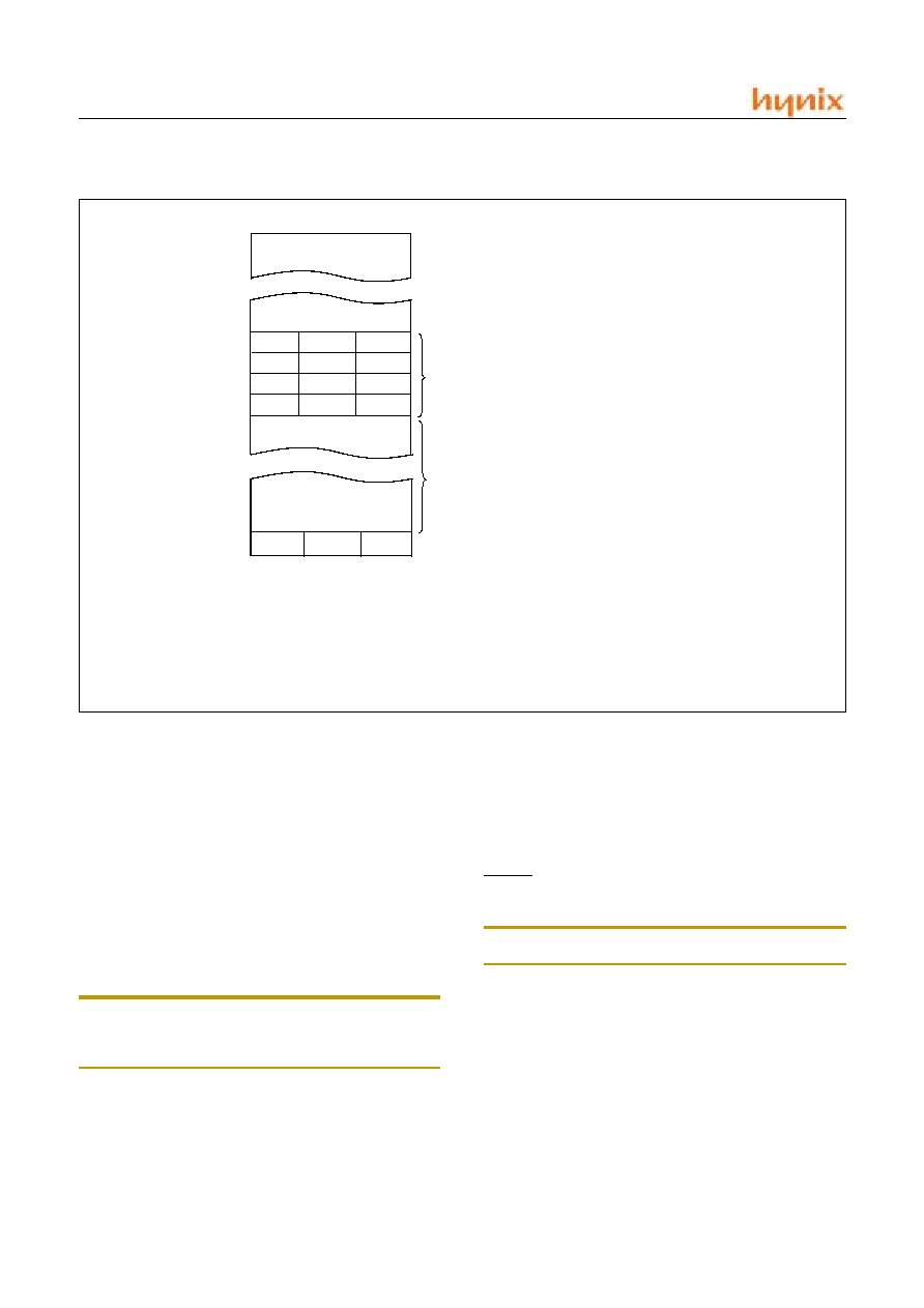
HMS77C2000/2001
48
Nov. 2002 Ver 1.1
Example: Customer Code D1D2
H
The Customer ID code "D1D2
H
" should be stored in the
ID locations 200
H
~ 203
H
like this (HMS77C2000):
2000
:
0000 0000 1101
2001
:
0000 0000 0001
2002
:
0000 0000 1101
2003
:
0000 0000 0010
Reading these four memory locations, even with the code
protection bit programmed would still output on UP0 the
bit sequence "1101", "0001", "1101", "0010" which is
"D1D2
H
".
Note: All other locations in HMS77C2000/2001 configura-
tion memory are reserved and should not be pro-
grammed.
13.2.4 Program / Verify Mode
The program/verify mode is entered by holding pins UP0,
UP1 and the other pins low while raising V
PP
pin from V
IL
to V
IHH
. Once in this mode the user program memory and
the configuration memory can be accessed and pro-
grammed in a serial fashion. The mode of operation is se-
rial. UP0 and UP1 are Schmitt Trigger inputs in this mode.
The sequence that enters the device into the programming/
verify mode places all other logic into the reset state (the
RESET pin was initially at V
IL
). The means that all I/O are
in the reset state (high impedance inputs).
Note: All other pins except UP0 and UP1 must be low.
Program/Verify Operation
The UP1 pin is used as a clock input pin. and the UP0 pin
is used for entering command bits and data input/output
during serial operation.
To input a command, the clock pin (UP1) is cycled six
times. Each command bit is latched on the falling edge of
the clock with the LSB of the command being input first.
The data on pin UP0 is required to have a minimum setup
and hold time (See AC/DC spec.) with respect to the fall-
FIGURE 13-2 SERIES PROGRAM MEMORY MAP IN PROGRAM/VERIFY MODE
For Customer Use
0
0
0
0
0
0
0
0
ID0
ID1
ID2
ID3
(4x4 bit usable)
For Factory Use
Cofiguration word 6 bits
FFF
H
Address
000
H
11
0
Bit Number
Use porgram Memory
(NNN
H
+1)x12 bit
NNN
H
TTT
H
TTT
H
+ 1
TTT
H
+ 2
TTT
H
+ 3
TTT
H
+ 3F
H
NNN
H
: Highest normal EPROM memory address.
NNN
H
= 1FF
H
for HMS77C2000, NNN
H
= 3FF
H
for HMS77C2001
Note that some versions will have an oscillator calibration value
programmed at NNN
H
.
TTT
H
: Start address of special EPROM area and ID locations.
TTT
H
= 200
H
for HMS77C2000
TTT
H
= 400
H
for HMS77C2001
HMS77C2000/2001
Nov. 2002 Ver 1.1
49
ing edge of the clock.
Commands that have data associated with them (read and
load) are specified to have a minimum delay of 1us be-
tween the command and the data. After this delay the clock
pin is cycled 16 times with the first cycle being a start bit
and the last cycle being a stop bit. Data is also input and
output LSB first. Therefore, during a read operation the
LSB will be transmitted onto pin UP0 on the rising edge
of the second cycle, and during a load operation the LSB
will be latched on the falling edge of the second cycle. A
minimum 1us delay is also specified between consecutive
commands.
All commands are transmitted LSB first. Data words are
also transmitted LSB first. The data is transmitted on the
rising edge and latched on the falling edge of the clock. To
allow for decoding of commands and reversal of data pin
configuration, a time separation of at least 1us is required
between a command and a data word (or another com-
mand).
- Load
Data
After receiving this command, the chip will load
in a 14-bit "data word" when 16 cycles are ap-
plied, as described previously. Because this is a
12bit core, the two MSB's of the data are ig-
nored.
A timing diagram for the load data command is
shown in Figure 13-4.
- Read
Data
After receiving this command, the chip will trans-
mit data bits out of the memory currently access-
ed starting with the second rising edge of the
clock input. The UP0 pin will go into output mode
on the second rising clock edge, and it will revert
back to input mode (hi-impedance) after the 16th
rising edge.
Because this is a 12 bit core, the two MSB's of
the data are unused and read as `0'. A timing di-
agram of this command is shown in Figure 13-5.
- Increment
Address
The PC is incremented when this command is
received. A timing diagram of this command is
shown in Figure 13-6.
- Begin
Programming
A load data command must be given before ev-
ery begin programming command.
Programming of the appropriate memory (test
program memory or user program memory) will
begin after this command is received and decod-
ed. Programming should be performed with a se-
ries of 100us programming pulses.
A programming pulse is defined as the time be-
tween the begin programming command and the
End programming command.
- End
Programming
As soon as receiving end programming com-
mand, the chip stops programming the memory
(configuration program memory or user program
memory) that it was programming at the time.
13.3 CONFIGURATION WORD
The HMS77C2000 and HMS77C2001 devices have sever-
al configuration bits. These bits can be programmed (reads
`0') or left unprogrammed (reads `1') to select various de-
vice configurations.
Command
Mapping
(MSB ... LSB)
Data
Load data
0 0 0 0 1 0
0, data(14),0
Read data
0 0 0 1 0 0
0, data(14),0
Increment address
0 0 0 1 1 0
Begin programming
0 0 1 0 0 0
End programming
0 0 1 1 1 0
TABLE 13-1 COMMAND MAPPING
HMS77C2000/2001
50
Nov. 2002 Ver 1.1
13.4 CODE PROTECTION
The program code written into the EPROM can be protect-
ed by writing to the CP bit of the configuration word. In the
HMS77C2000 and HMS77C2001, it is still possible to
program and read locations 000
H
through 03F
H
, after code
protection. Once code protection is enabled, all code pro-
tected locations read 555
H
and prevented from further pro-
gramming. All unprotected segments, including the
internal oscillator calibration value, ID, and configuration
word read as normal. These locations can be programmed.
13.4.1 Embedding Configuration Word and ID
information in the Hex File
To allow portability of code, the programmer is required to
read the configuration word and ID locations from the hex
file when loading the hex file. If configuration word infor-
mation was not present in the hex file then a simple warn-
ing message may be issued. Similarly, while saving a hex
file, configuration word and ID information must be in-
cluded. An option to not include this information may be
provided.
FIGURE 13-3 CONFIGURATION WORD FOR HMS77C2000/1
bit11
bit0
4
3
2
1
PORLS: Power on reset level selection bit
1 = 1.7v(Typ.)
0 = Data retention voltage 0.6v(Typ.)
RESETE: RESET pin enable bit.
1 = RESET pin enabled
0 = RESET tied to
V
DD
(internally).
CP: Code protection bit.
1 = Code protection off
0 = Code protection on
WDTE: Watchdog timer enable bit
1 = WDT enabled
0 = WDT disabled
FOSC1~FOSC0: Oscillator selection bits
11 = ERC - external RC oscillator
10 = IRC - internal RC oscillator
01 = XT oscillator
00 = LF oscillator
Address
: FFF
H
CP
WDTE FOSC1 FOSC0
-
Unimplemented, read as `0'
Configuration Word
RESETE
PORLS
5
Program Memory Segment
R/W in Protected Mode
R/W in Unprotected Mode
Configuration Word (FFF
H
)
R/W Enable
R/W Enable
00
H
~ 3F
H
R/W Enable
R/W Enable
40
H
~ 1FE
H
Read Disable (555
H
), Write Disable
R/W Enable
1FF
H
Oscillator Calibration Value
R/W Enable
R/W Enable
ID Location (200
H
~ 203
H
)
R/W Enable
R/W Enable
TABLE 13-2 CODE PROTECTION(HMS77C2000)

HMS77C2000/2001
Nov. 2002 Ver 1.1
51
13.4.2 Checksum Calculations
Checksum is calculated by reading the contents of the
HMS77C2000 and HMS77C2001 memory locations and
adding up the opcodes up to the maximum user address-
able location, (not including the last location which is re-
served for the oscillator calibration value).
Any carry bits exceeding 16-bits are neglected. Finally, the
configuration word (appropriately masked) is added to the
checksum. Checksum computation for the HMS77C2000
and HMS77C2001 are shown in Table 13-4 .
The checksum is calculated by summing the following:
- The contents of all program memory locations
- The configuration word, appropriately masked
- Masked ID locations (when applicable)
The least significant 16 bits of this sum is the checksum
The following table describes how to calculate the check-
sum for each device. Note that the checksum calculation
differs depending on the code protect setting.
Since the program memory locations read out differently
depending on the code protect setting, the table describes
how to manipulate the actual program memory values to
simulate the values that would be read from a protected de-
vice. When calculating a checksum by reading a device,
the entire program memory can simply be read and
summed. The configuration word and ID locations can al-
ways be read.
The oscillator calibration value location is not used in the
above checksums.
Program Memory Segment
R/W in Protected Mode
R/W in Unprotected Mode
Configuration Word (FFF
H
)
R/W Enable
R/W Enable
00
H
~ 3F
H
R/W Enable
R/W Enable
40
H
~ 3FE
H
Read
Disable(555
H
), Write Disable
R/W Enable
3FF
H
Oscillator Calibration Value
R/W Enable
R/W Enable
ID Location (400
H
~ 403
H
)
R/W Enable
R/W Enable
TABLE 13-3 CODE PROTECTION(HMS77C2001)
Device
Code Protect
Checksum
HMS77C2000
OFF
ON
SUM [000
H
~ 1FE
H
] + CFGW & 03F
H
SUM [000
H
~ 03F
H
] + CFGW & 03F
H
+ SUM(IDS)
HMS77C2000
OFF
ON
SUM [000
H
~ 3FE
H
] + CFGW & 03F
H
SUM [000
H
~ 03F
H
] + CFGW & 03F
H
+ SUM(IDS)
TABLE 13-4 CHECKSUM COMPUTATION
Legend: CFGW = Configuration Word
SUM[a~b] = [ Sum of locations a through b inclusive]
SUM_ID = ID locations masked by F
H
then made into a 16 bit value with ID0 as the most significant nibble.
For example, ID0 = 12
H
, ID1 = 37
H
, ID2 = 4
H
, ID0 = 26
H
, then SUM_ID = 2746
H
.
Checksum = [Sum of all the individual expressions] MODULO [FFFF
H
]
+ = addition, & = Bitwise AND

HMS77C2000/2001
52
Nov. 2002 Ver 1.1
13.5 PROGRAM/VERIFY MODE ELECTRICAL CHARACTERISTICS
Parameter
Sym.
Characteristic
Min.
Typ.
Max.
Unit
Condition
PD1
V
DDP
Supply voltage
4.75
5.0
5.25
V
PD2
I
DDP
Supply current during programming
20
mA
from V
DD
PD3
V
DDV
Supply voltage during verify
V
DDMIN
V
DDMAX
V
Note
1
PD4
V
IHH
Induced Voltage for program mode entry
11.25
11.5
11.75
V
PD5
I
PP
Programming supply current
50
mA
from V
PP
PD6
V
IH1
UP0, UP1 input high level
0.8 V
DD
V
DD
V
Schmit
Trigger
Input
PD7
V
IL1
UP0, UP1 input low level
0
0.2V
DD
V
Schmitt
Trigger
Input
P1
T
R
V
PP
pin rising time
-
-
1
ms
P2
T
F
V
PP
pin falling time
-
-
1
ms
P3
T
SET1
Data in setup time before clock
100
ns
P4
T
HLD1
Data in hold time before clock
100
ns
P5
T
DLY1
Data input not driven to next clock input
(delay required between command/data or
command/command)
1.0
us
P6
T
DLY2
Delay between clock
to clock
of
next command or data
1.0
us
P7
T
DLY2
Clock
to data out valid (during read data)
200
ns
P8
T
HLD0
Hold time after V
PP
2
us
TABLE 13-5 AC/DC CHARACTERISTICS TIMING REQUIREMENTS FOR PROGRAM/VERIFY MODE
1. Program must be verified at the minimum and maximum V
DD
limits for the part.
HMS77C2000/2001
Nov. 2002 Ver 1.1
53
FIGURE 13-4 LOAD DATA COMMAND (PROGRAM/VERIFY)
V
IHH
11V
10V
P8
1
2
3
4
5
6
1
2
3
4
5
15
100ns
P6
1us
MIN
P5
1us
MIN
P3
P4
100ns
MIN
0
1
0
0
0
0
0
P3
P4
100ns
MIN
~~
~~
RESET/V
PP
Program/Verify Mode
UP1(Clock)
UP0(Data)
Reset
FIGURE 13-5 READ DATA COMMAND(PROGRAM/VERIFY)
V
IHH
11V
10V
P8
1
2
3
4
5
6
1
2
3
4
15
100ns
P6
1us
MIN
P5
1us
MIN
P3
P4
100ns
MIN
0
0
1
0
0
0
0
RESET/V
PP
Program/Verify Mode
UP1(Clock)
UP0(Data)
14
16
~~
Reset
B0
B1
B10
~~
~~
...
B11
0
0
UP0=Input
UP0=Output
UP0=Input
HMS77C2000/2001
54
Nov. 2002 Ver 1.1
FIGURE 13-6 INCREMENT ADDRESS (PROGRAM/VERIFY
V
IHH
11V
10V
P8
1
2
3
4
5
6
1
2
100ns
P6
1us
MIN
P5
1us
MIN
P3
P4
100ns
MIN
0
1
1
0
0
0
RESET/V
PP
Program/Verify Mode
UP1(Clock)
UP0(Data)
Reset
Next Command
0
0
FIGURE 13-7 BEGIN & END PROGRAMMING(PROGRAM/VERIFY)
V
IHH
11V
10V
P8
1
2
3
4
5
6
1
2
3
4
5
100us
0
0
1
0
0
RESET/V
PP
UP1(Clock)
UP0(Data)
6
"Begin Programming"
"End Programming"
0
0
1
1
1
0
0
Programming Pulse
(internal Signal)
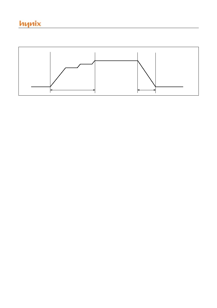
HMS77C2000/2001
Nov. 2002 Ver 1.1
55
FIGURE 13-8 V
PP
RISING & FALLING
RESET/V
PP
11V
10V
V
IHH
P1(T
R
)
P2(T
F
)

HMS77C2000/2001
56
Nov. 2002 Ver 1.1
SALES NETWORKS
KOREA
SINGAPORE
HYNIX Semiconductor Inc. Seoul Office.
HYNIX Semiconductor Asia Pte. Ltd.
Young Dong Bldg, 891 Daechi-dong
,
Kangnam-gu Seoul Korea
7 Temasek Boulevard Suntec Tower One #42-02 Singapore 038987
Tel : 02-3459-3837
Tel : 65-432-4553
Fax : 02-3459-3945
Fax : 65-336-5933
U.S.A
TAIWAN
HYNIX Semiconductor America Inc.
HYNIX Semiconductor Taiwan Inc.
3101 North First Street San Jose, CA 95134
8FI., No.161, Section 2, Minsheng East Road., Taipei, Taiwan, R.O.C
Tel : 1-408-232-8152
Tel : 886-2-2500-8357
Fax : 1-408-232-8135
Fax : 886-2-2509-8977
HONGKONG
DEUTSCHLAND
HYNIX Semiconductor Hongkong Ltd.
HYNIX Semiconductor Deutschland GmbH.
Rm 1602, 16F., Bank of America Tower 12 Harcourt Road, HongKong
Frankfurter Str., 107 D-65479 Raunheim, Germany
Tel : 852-2971-1614
Tel : 49-6142-921-343
Fax : 852-2971-1622
Fax : 49-6142-921-214
BEIJING OFFICE
UNITED KINGDOM
HYNIX Semiconductor Inc. Beijing Office.
HYNIX Semiconductor U.K. Ltd.
Rm. 1902 Landmark Tower, 8 North Dongsanhuam Road, Chaoyang District
Beijing 100004 P.R. China
241 Brooklands Road, Weybridge, Surrey, KT13 ORH, U.K.
Tel : 86-10-6590-6934
Tel : 44-1932-827-733
Fax : 86-10-6590-0908
Fax : 44-1932-827-7746
SHANGHAI OFFICE
JAPAN
HYNIX Semiconductor Inc. Shanghai Office.
HYNIX Semiconductor Japan Inc.
3F., Tianhong Bldg. 80 Xianxia R/d, Shanghai, China
Yurakucho-Denki Bld. North 9F 1-7-1, Yurakucho, Chiyoda-Ku, Tokyo,
Japan
Tel : 86-21-6257-5522
Tel : 81-3-3211-1911
Fax : 86-21-6209-2686
Fax : 81-3-3211-5447~8