HMS81C2232/48 HMS81C2332/48
FEB. 2003 Ver 1.00
1
HMS81C2232/48, HMS81C2332/48
CMOS Single-Chip 8-Bit Microcontroller
with VFD Controller & VFD Driver
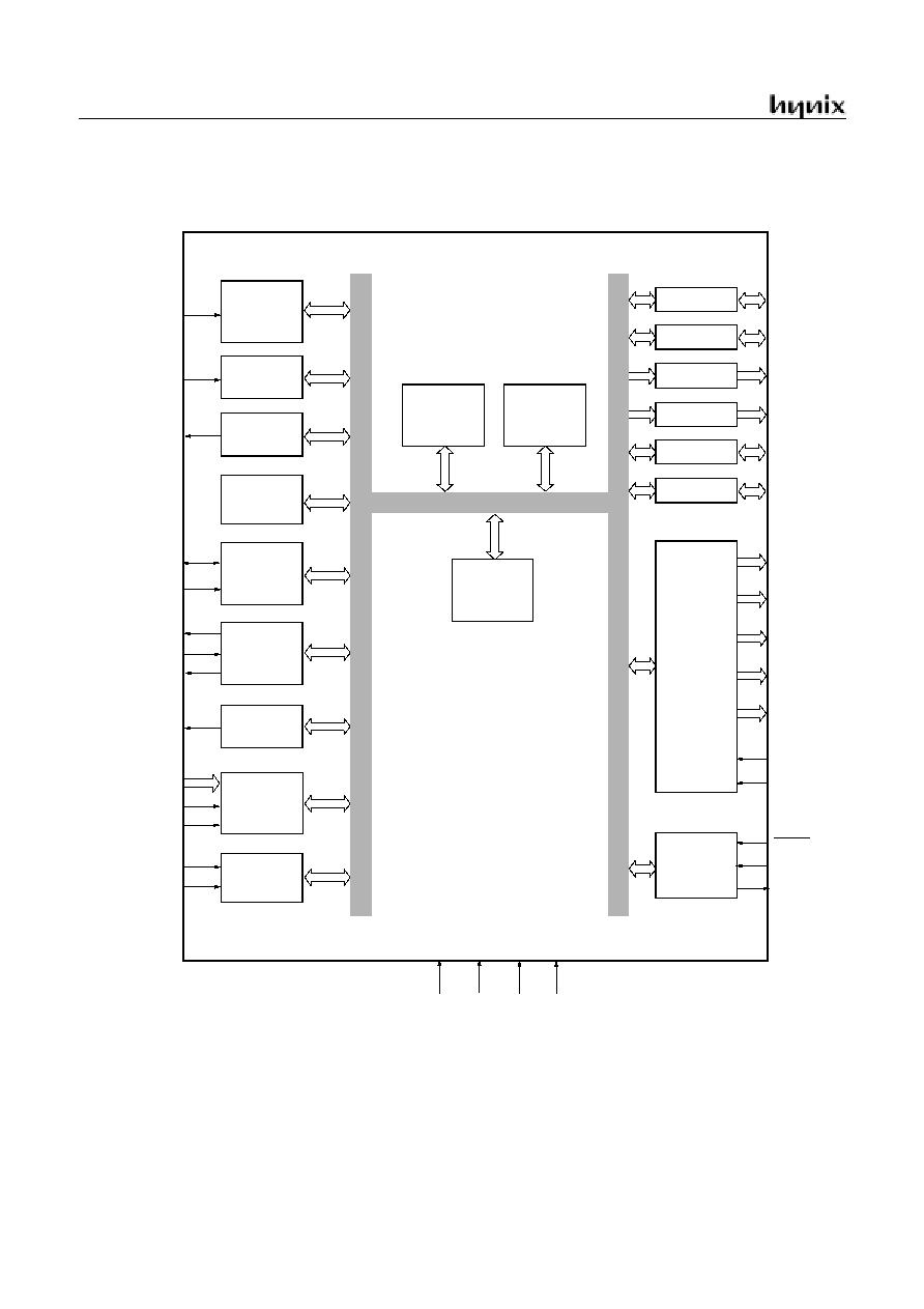
1. OVERVIEW
1.1 Description
The HMS81C2232/48 is advanced CMOS 8-bit micro-controller with 32/48K bytes of ROM(EPROM). This is a powerful micro-controller
which provides a highly flexible and cost effective solution to many VFD applications. This provides the following standard features : 32K/
48K bytes of ROM(EPROM), 1K bytes of RAM, 8-bit timer/counter, 8-bit A/D converter, 6-bit Watch dog Timer, Programmable Buzzer
Driving Port, Serial Peripheral Interface, 8-bit remote control timer, on-chip oscillator and clock circuitry. It also comes with high voltage
I/O pins that can directly drive a VFD(Vacuum Fluorescent Display). In addition, the HMS8XC2232/48 support power saving modes to
reduce power consumption.
1.2 HMS81C2232/48 Features
� 32K/48K bytes ROM(EPROM)
� 896 Bytes of On-Chip Data RAM
(Including STACK Area)
� 112 Bytes of On-Chip Display RAM
� Minimum Instruction Execution time:
- 1uS at 4MHz (2cycle NOP Instruction)
� One 8-bit Basic Interval Timer
� One 7-bit Watch Dog Timer
� Two 8-bit Timer/Counters
� 10-bit High Speed PWM Output
� Two 8-bit Serial Peripheral Interface
� Two External Interrupt Ports
� One Programmable 6-bit Buzzer Driving Port
� 53 FIP Ports
- 16EA Output only pins
- High-voltage pins Max. 40V
� Operating Temperature
-40�C ~ 85�C
� 12 Interrupt Sources
- Two External Sources (INT0, INT1)
- Two Timer/Counter Sources (Timer0, Timer1)
- Three Remote Timer Sources(FE,RE,OVF)
- Two SPI Sources(SIO1, SIO3)
- Three Functional Sources (ADC,WDT,BIT)
� 7-Channel 8-bit On-Chip Analog to Digital Con-
verter
� Oscillator:
- Crystal
- Ceramic Resonator
� Low Power Dissipation Modes
- STOP Mode
- SLEEP Mode
� Operating Voltage: 2.7V ~ 5.5V (@8MHz)
4.5V ~ 5.5V (@10MHz)
� Operating Frequency: 1MHz ~ 10MHz
� Enhanced EMS Improvement
Power Fail Processor
(Noise Immunity Circuit)
Device Name
ROM Size
RAM Size
Display RAM
OTP
Package
HMS81C2232
32K bytes
896 bytes
112bytes
HMS87C2232
80TQFP
80MQFP
HMS81C2248
48K bytes
HMS87C2248
HMS81C2332
32K bytes
896 bytes
112bytes
HMS87C2332
64SDIP,64LQFP
64MQFP
HMS81C2348
48K bytes
HMS87C2348
HMS81C2232/48 HMS81C2332/48
2
FEB. 2003 Ver 1.00
Preliminary
1.3 HMS2332/48 Features
� 32K/48K bytes ROM(EPROM)
� 896 Bytes of On-Chip Data RAM
(Including STACK Area)
� 112 Bytes of On-Chip Display RAM
� Minimum Instruction Execution time:
- 1uS at 4MHz (2cycle NOP Instruction)
� One 8-bit Basic Interval Timer
� One 7-bit Watch Dog Timer
� Two 8-bit Timer/Counters
� 10-bit High Speed PWM Output
� Two 8-bit Serial Peripheral Interface
� Two External Interrupt Ports
� One Programmable 6-bit Buzzer Driving Port
� 41 FIP Ports
- 12EA Output only pins
- High-voltage pins Max. 40V
� Operating Temperature
-40�C ~ 85�C
� 11 Interrupt Sources
- Two External Sources (INT0, INT1)
- Two Timer/Counter Sources (Timer0, Timer1)
- Three Remote Timer Sources(FE,RE,OVF)
- One SPI Sources(SIO1)
- Three Functional Sources (ADC,WDT,BIT)
� 5-Channel 8-bit On-Chip Analog to Digital Con-
verter
� Oscillator:
- Crystal
- Ceramic Resonator
� Low Power Dissipation Modes
- STOP Mode
- SLEEP Mode
� Operating Voltage: 2.7V ~ 5.5V (@8MHz)
4.5V ~ 5.5V (@10MHz)
� Operating Frequency: 1MHz ~ 10MHz
� Enhanced EMS Improvement
Power Fail Processor
(Noise Immunity Circuit)
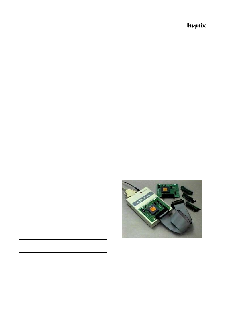
1.4 Development Tools
The HMS81C22xx/23xx are supported by a full-featured macro
assembler, an in-circuit emulator CHOICE-Dr.
TM
and OTP pro-
grammers. There are third different type programmers such as
emulator add-on board type, single type, gang type. For mode de-
tail, Refer to "25. OTP PROGRAMMING" on page 112. Macro
assembler operates under the MS-Windows 95, 98, NT, 2000,
XP
TM
.Please contact sales part of Hynix Semiconductor.
In Circuit
Emulators
CHOICE-Dr.
Socket Adapter
for OTP
OA87C23XX-64SD (64SDIP)
OA87C23XX-64QF (64MQFP)
OA87C23XX-64QT (64LQFP)
OA87C22XX-80QF (80MQFP)
OA87C22XX-80QT (64TQFP)
POD
CHPOD81C22D-64SD (64SDIP)
Assembler
HYNIX Macro Assembler

HMS81C2232/48 HMS81C2332/48
FEB. 2003 Ver 1.00
3
1.5 Ordering Information
HMS81C22xx
Device name
ROM Size
RAM size
Package
Mask version
HMS81C2232 Q
HMS81C2232 TQ
HMS81C2248 Q
HMS81C2248 TQ
32K bytes
32K bytes
48K bytes
48K bytes
896 bytes
80MQFP
80TQFP
80MQFP
80TQFP
OTP version
HMS81C2232 Q
HMS81C2232 TQ
HMS81C2248 Q
HMS81C2248 TQ
32K bytes OTP
32K bytes OTP
48K bytes OTP
48K bytes OTP
896 bytes
80MQFP
80TQFP
80MQFP
80TQFP
HMS81C23xx
Device name
ROM Size
RAM size
Package
Mask version
HMS81C2332 K
HMS81C2332 Q
HMS81C2332 LQ
HMS81C2348 K
HMS81C2348 Q
HMS81C2348 LQ
32K bytes
32K bytes
32K bytes
48K bytes
48K bytes
48K bytes
896 bytes
64SDIP
64MQFP
64LQFP
64SDIP
64MQFP
64LQFP
OTP version
HMS87C2332 K
HMS87C2332 Q
HMS87C2332 LQ
HMS87C2348 K
HMS87C2348 Q
HMS87C2348 LQ
32K bytes OTP
32K bytes OTP
32K bytes OTP
48K bytes OTP
48K bytes OTP
48K bytes OTP
896 bytes
64SDIP
64MQFP
64LQFP
64SDIP
64MQFP
64LQFP