
HYNIX SEMICONDUCTOR INC.
8-BIT SINGLE-CHIP MICROCONTROLLERS
HMS81C4x60
User's Manual (Ver. 1.1)

Version 1.1
Published by MCU Application Team
Heung-il Bae(hibae@hynix.com), Byoung-jin Lim( bjinlim@hynix.com)
©2001
Hynix Semiconductor Inc. All rights reserved.
Additional information of this manual may be served by Hynix Semiconductor offices in Korea or Distributors and Repre-
sentatives listed at address directory.
Hynix Semiconductor reserves the right to make changes to any information here in at any time without notice.
The information, diagrams and other data in this manual are correct and reliable; however, Hynix Semiconductor is in no
way responsible for any violations of patents or other rights of the third party generated by the use of this manual.

HMS81C4x60
November 2001 Ver 1.1
1
HMS81C4x60
CMOS SINGLE-CHIP 8-BIT MICROCONTROLLER
FOR TELEVISION
1. OVERVIEW
1.1 Description
The HMS81C4x60 is an advanced CMOS 8-bit microcontroller with 60K bytes of ROM. This is one of the HMS800 family.
This is a powerful microcontroller which provides a high flexibility and cost effective solution to many TV applications. The
HMS81C4x60 provides following standard features: 60K bytes of ROM, 1024 bytes of RAM, 8/16-bit timer/counter, on-
chip PLL oscillator and clock circuitry. In addition, there are other package types, HMS81C4360(32PDIP),
HMS81C4360SK(32SKDIP), HMS81C4460(42SDIP).
This document is explained for the base of HMS81C4x60, the eliminated functions are same as below.
1.2 Features
∑ 60K Bytes of On-chip Program Memory
∑ 1024 Bytes of On-chip Data RAM
∑ Minimum Instruction Cycle Time
- 256ns (NOP operation)
∑ PLL Oscillator for OSD and System Clock
- External 4MHz Crystal Input
∑ 31 Programmable I/O pins
- 26 Input/Output and 5 Input pins
∑ I
2
C Bus Interface
- Multimaster (2 Pairs interface pins)
∑ A/D Converter
- 8-bit
◊ 5
ch
∑ Pulse Width Modulation
- 14-bit
◊ 1
ch
- 8-bit
◊ 5
ch
∑ Timer
- Timer/Counter : 8-bit
◊ 4
ch(16-bit
◊
2 ch)
- Basic interval timer
- Watch Dog Timer
∑ Number of Interrupt Source
- 16 Interrupts
- 3 External Interrupts
∑ On Screen Display
- 512 character fonts pattern
- Character Size : 1.0, 1.5, 2.0 times
- Character Pixel size : 12
◊
10, 12
◊
12, 12
◊
14,
12
◊
16, 16
◊
18
- Display Capability : 48 Characters
◊
16 Lines
- Character, Background color : 512 colors, 8 pal-
let
- Special functions : Rounding, Outline, Shadow,
Underline, Double scanned line OSD
∑ Buzzer Driving Port
- 500Hz ~ 250KHz @4MHz (Duty 50%)
∑ Vertical Blanking Interveral Information cap-
ture for EIA-608(Closed Caption) or VPS, etc
Device name
ROM Size
EPROM Size
RAM Size
I/O
Package
HMS81C4260
60K bytes
-
1024bytes
31
52SDIP
HMS87C4260
60K bytes
1024bytes
31
52SDIP
HMS81C4x60
2
November 2001 Ver 1.1
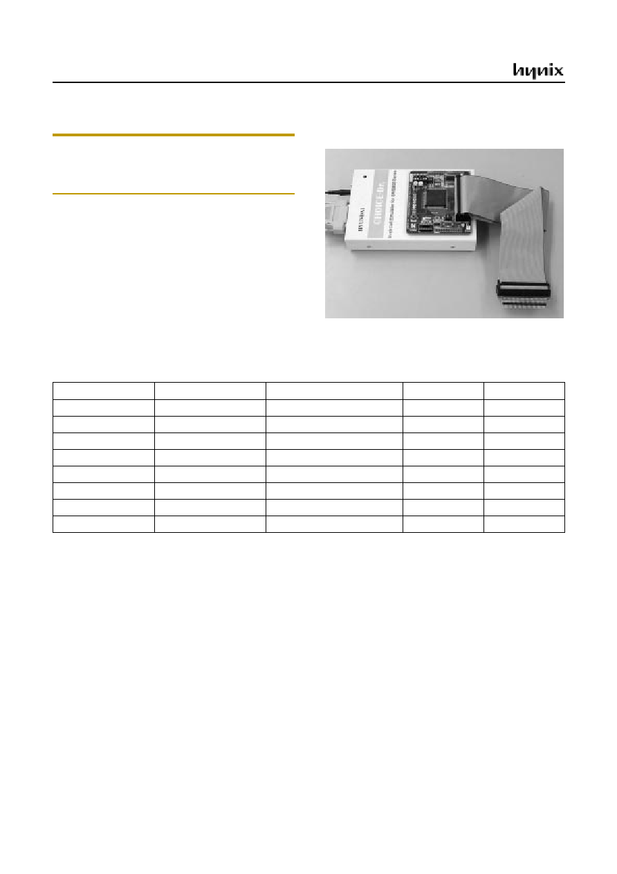
1.3 Development Tools
Note: There are several setting switches in the Emulator.
User should read carefully and do setting properly before
developing the program. Otherwise, the Emulator may not
work properly.
The HMS87C4x60 is supported by a full-featured macro assem-
bler, an in-circuit emulator CHOICE-Dr.
TM
and EPROM pro-
grammers. There are two different type programmers such as
single type and gang type. For more detail, refer to EPROM Pro-
gramming chapter. Macro assembler operates under the MS-
Windows 95/98
TM
.
Please contact sales part of Hynix Semiconductor.
1.4 Ordering Information
Device name
ROM Size (bytes)
RAM size
Package
Mask ROM version
HMS81C4260
60K bytes
1024 bytes
52SDIP
OTP ROM version
HMS87C4260
60K bytes EPROM (OTP)
1024 bytes
52SDIP
Mask ROM version
HMS81C4360SK
60K bytes
1024 bytes
32SKDIP
OTP ROM version
HMS87C4360SK
60K bytes EPROM (OTP)
1024 bytes
32SKDIP
Mask ROM version
HMS81C4360
60K bytes
1024 bytes
32PDIP
OTP ROM version
HMS87C4360
60K bytes EPROM (OTP)
1024 bytes
32PDIP
Mask ROM version
HMS81C4460
60K bytes
1024 bytes
42SDIP
OTP ROM version
HMS87C4460
60K bytes EPROM (OTP)
1024 bytes
42SDIP

HMS81C4x60
November 2001 Ver 1.1
3
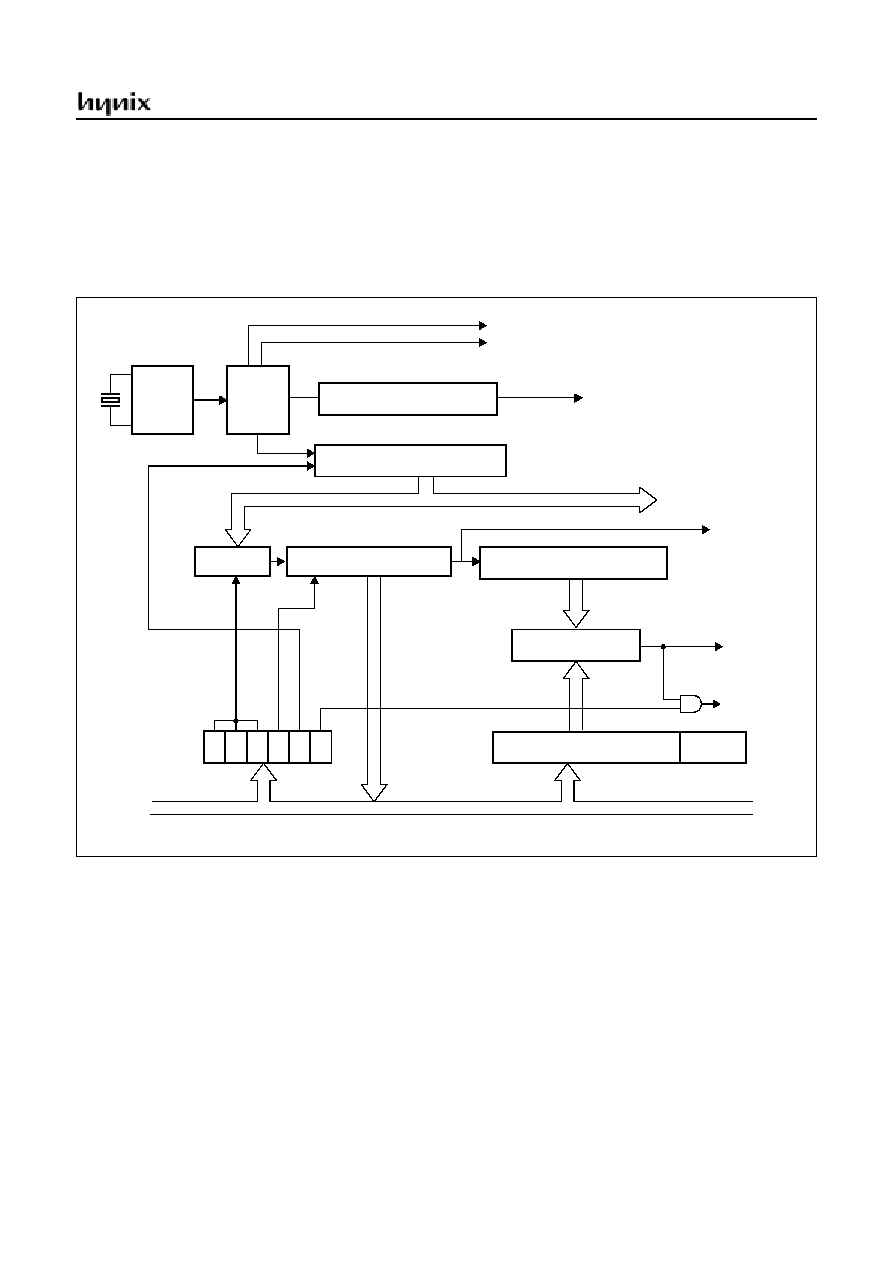
2. BLOCK DIAGRAM
Figure 2-1 Block Diagram
PWM
I
2
C
TIMER
PRESCALER
/BIT
WATCH DOG
BUZZER
REMOCON
INTERRUPT
G8MC
CORE
R4 PORT
RAM ( 1024)
MASK ROM
( User ROM
: 60KB
Font ROM
: 32KB )
PLL
CLOCK
ADC
D A TA
OSD
R10/AN0
R11/AN1
R12/AN2
R13/AN3
R14/AN4
R30/PWM0
R31/PWM1
R32/PWM2
R33/PWM3
R 34/PW M 4
R 35/PW M 5
R40/SCL0
R41/SDA0
R 42/S C L1
R 43/SD A1
R 24/EC 2
R 25/EC 3
CVBS
R
G
B
YM
YS
R 36/BU Z
R 37/TM R 1
R
2
1/INT
1
R
2
2/INT
2
VS
HS
TES
T
Vd
d
RE
SET
Xin
X
out
Vs
s
SCAP
R3 PORT
R2 PORT
R1 PORT
R0 PORT
CONTROLLER
TIMER
GENERATION
/ SYSTEM
CONTROLLER
SLICER
R 40 ~ R 43
R 30 ~ R 37
R 20 ~ R 25
R 10 ~ R 14
R 00 ~ R 07
R
2
3/INT
3
HMS81C4x60
4
November 2001 Ver 1.1
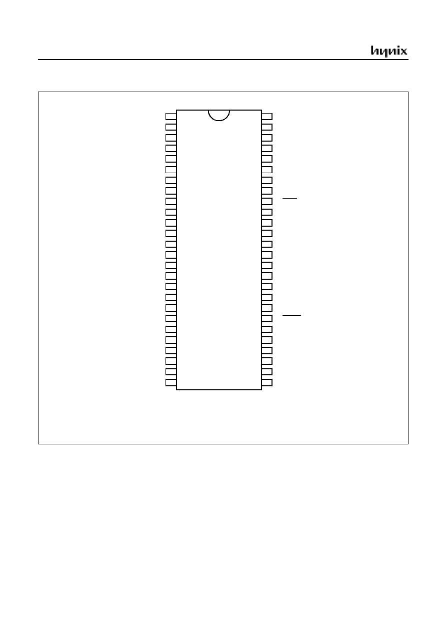
3. PIN ASSIGNMENT
Figure 3-1 52SDIP
R30/PWM0
R31/PWM1
YS
YM
R32/PWM2
R33/PWM3
R34/PWM4
R35/PWM5
R36/BUZ
R37/TMR1
TEST
VSS
B
G
R
VDD
VSS
XIN
XOUT
RESET
R03
R40/SCL0
R41/SDA0
CVBS
SCAP
R42/SCL1
R43/SDA1
R04
R05
R06
R07
VDD
R14/AD4
VDD
VSS
R10/AD0
R11/AD1
R12/AD2
R13/AD3
HS
VS
R20
1
2
12
11
3
4
5
6
7
8
9
10
13
14
15
16
17
18
19
20
21
52
51
41
42
50
49
48
47
46
45
44
43
40
39
38
37
36
35
34
33
32
HMS81C4260
R21/INT1
R22/INT2
R23/INT3
R24/EC2
R25/EC3
22
23
24
25
26
R02
VDD
VSS
R01
R00
31
30
29
28
27
52SDIP
HMS81C4x60
November 2001 Ver 1.1
5
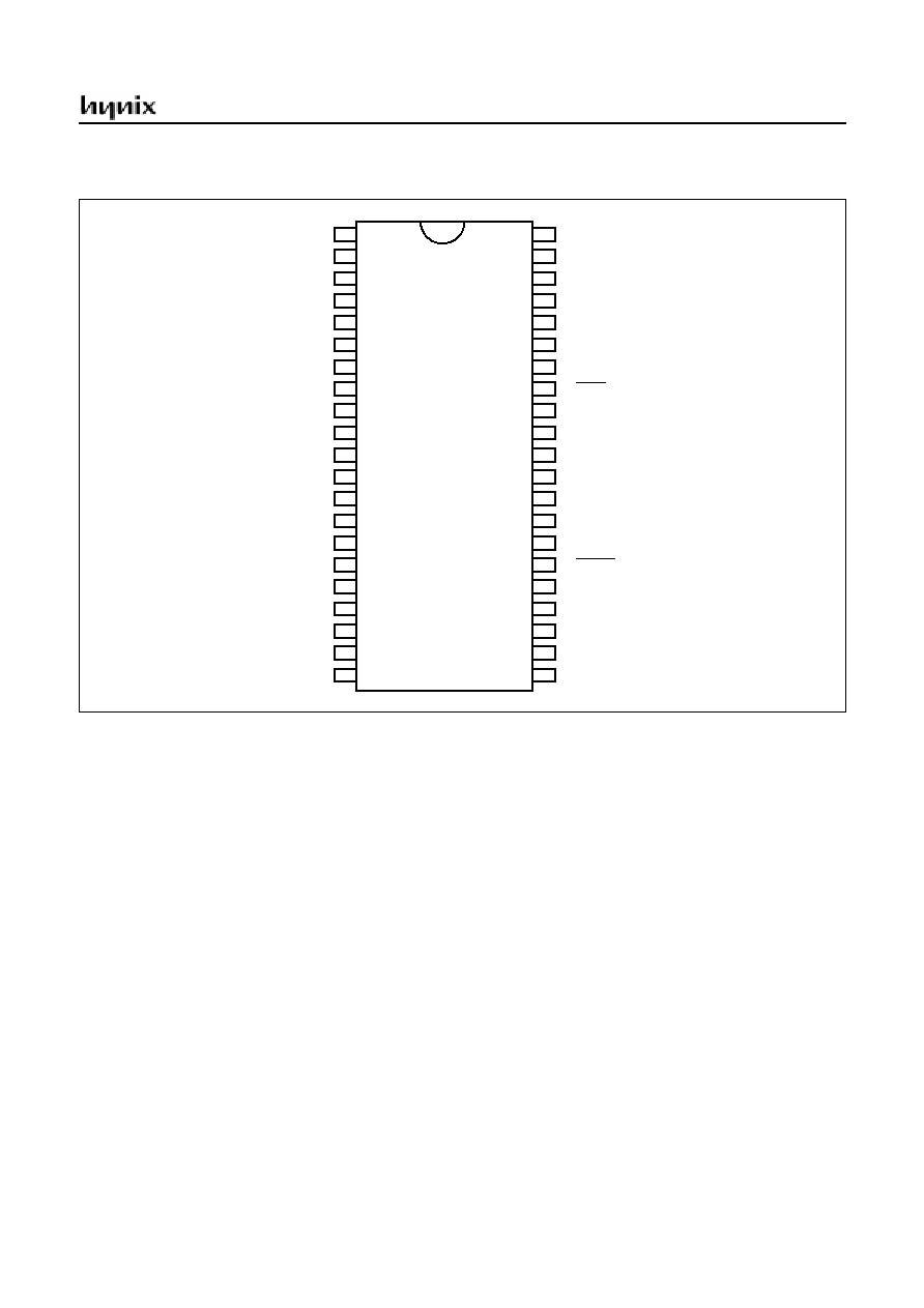
Figure 3-2 42SDIP
R31/PWM1
R32/PWM2
G
B
R33/PWM3
R34PWM4
R35/PWM5
R36/BUZ
R37/TMR1
TEST
YM
YS
R
XIN
XOUT
RESET
R03
R02
R01
R00
R25/EC3
R40/SCL0
R41/SDA0
R10/AD0
VSS
R42/SCL1
R43/SDA1
R04
VDD
R14/AD4
SCAP
CVBS
VDD
R11/AD1
R12/AD2
R13/AD3
HS
VS
R21/INT1
R22/INT2
R23/INT3
R24/EC2
1
2
12
11
3
4
5
6
7
8
9
10
13
14
15
16
17
18
19
20
21
42
41
31
32
40
39
38
37
36
35
34
33
30
29
28
27
26
25
24
23
22
HMS81C4460
42SDIP
HMS81C4x60
6
November 2001 Ver 1.1
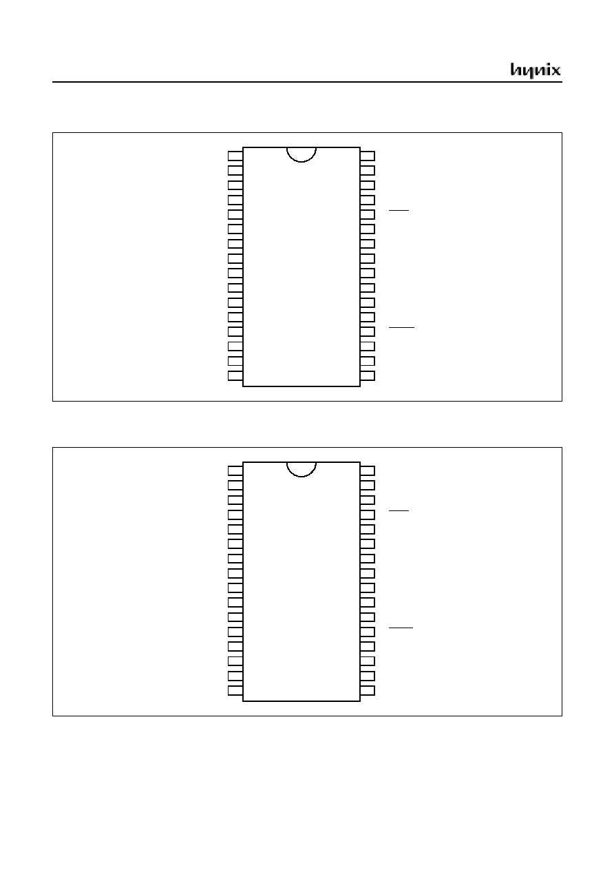
Figure 3-3 32SKDIP
Figure 3-4 32PDIP
HMS81C4360SK
R33/PWM3
R34/PWM4
XOUT
XIN
R35/PWM5
R37/TMR1
TEST
YM
YS
B
G
R
RESET
R02
R24/EC2
R23/INT3
R40/SCL0
R41/SDA0
R13/AD3
R10/AD0
R42/SCL1
R43/SDA1
VDD
R14/AD4
SCAP
CVBS
VDD
VSS
HS
VS
R21/INT1
R22/INT2
1
2
12
11
3
4
5
6
7
8
9
10
13
14
15
16
32
31
21
22
30
29
28
27
26
25
24
23
20
19
18
17
32SKDIP
HMS81C4360
R34PWM4
R35PWM5
RESET
XOUT
R37/TMR1
TEST
YM
YS
B
G
R
XIN
R02
R24/EC2
R23/INT3
R21/INT1
R40/SCL0
R41/SDA0
R11/AD1
R10/AD0
R42/SCL1
R43/SDA1
VDD
R14/AD4
SCAP
CVBS
VDD
VSS
R12/AD2
R13/AD3
HS
VS
1
2
12
11
3
4
5
6
7
8
9
10
13
14
15
16
32
31
21
22
30
29
28
27
26
25
24
23
20
19
18
17
32PDIP
HMS81C4x60
November 2001 Ver 1.1
7
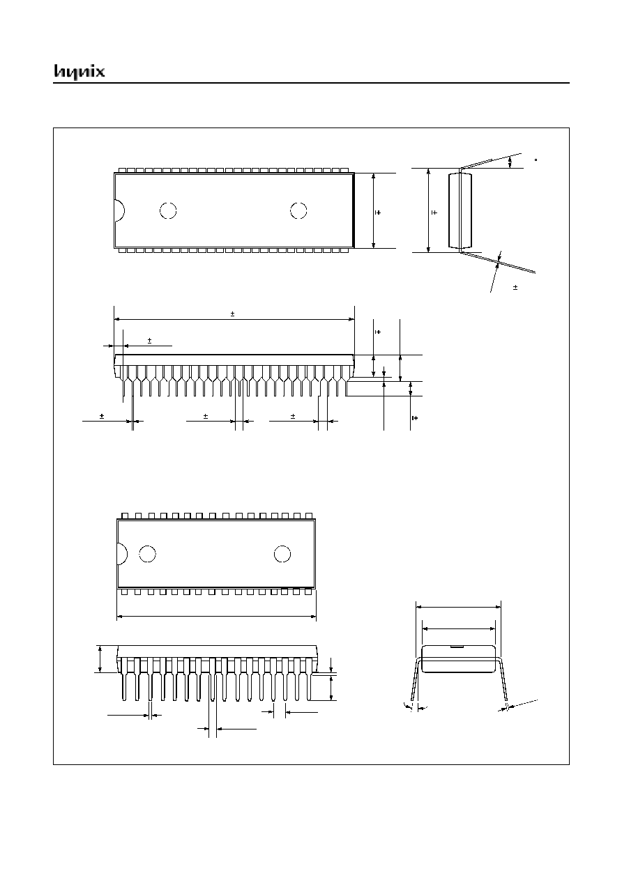
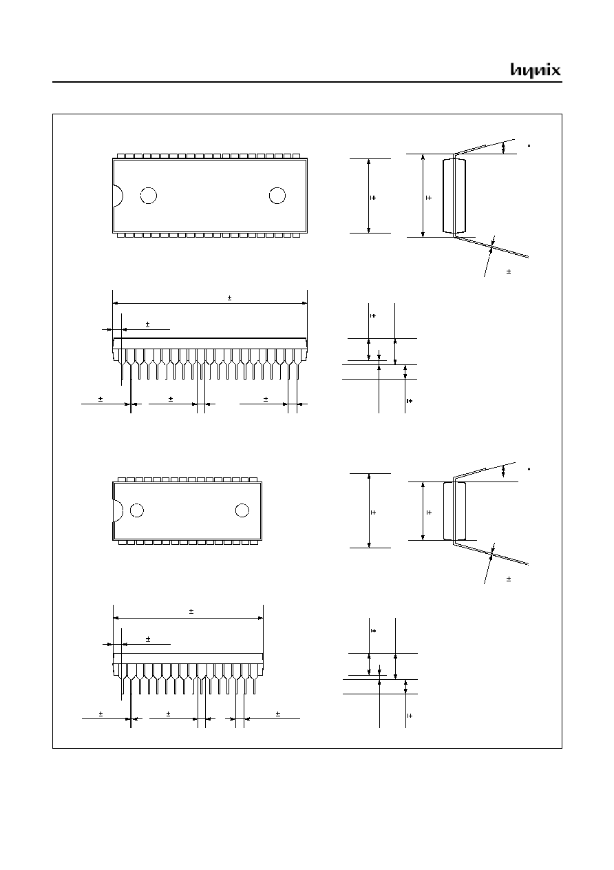
4. PACKAGE DIAGRAM
UNIT: mm
HYNIX
HMS81C4260
1
26
27
52
45.97
0.13
0.76
0.13
1.778
0.25
4.3
8
M
a
x.
13.
97
0.2
5
15.
24
0.2
5
0.47
0.13
1.02
0.25
3.8
1
0.
1
3
3.2
4
0.20
0.5
0
M
i
n.
0.25
0.05
0 ~ 15
1.665
0.015
0.065
0.1 BSC
TYP 0.600 BSC
0.550
0.01
2
0 ~ 15∞
MIN 0.015
0.140
0.530
0.00
8
0.
2 max
0.045
0.022
0.120
HYNIX
HMS81C4360
1.645
1
16
17
32
UNIT: inch
HMS81C4x60
8
November 2001 Ver 1.1
Figure 4-1 Package Diagram
UNIT: mm
HYNIX
HMS81C4460
1
21
22
42
36.83
0.13
0.76
0.13
1.778
0.25
4.3
8
M
a
x.
13.9
7
0.2
5
15.2
4
0.2
5
0.47
0.13
1.02
0.25
3.8
1
0.
1
3
3.2
4
0.20
0.5
0
M
i
n.
0.25
0.05
0 ~ 15
UNIT: mm
HYNIX
HMS81C4360SK
1
16
17
32
27.68
0.13
0.76
0.13
1.778
0.25
4.
3
8
M
a
x
.
10
.16
0.
2
5
8.
8
9
0.
2
5
0.47
0.13
1.02
0.25
3.
81
0.1
3
3.
2
4
0.
20
0.
5
0
M
i
n.
0.25
0.05
0 ~ 15
HMS81C4x60
November 2001 Ver 1.1
9
5. PIN FUNCTION
V
DD
: Supply voltage.
V
SS
: Circuit ground.
TEST: Used for shipping inspection of the IC. For normal
operation, it should not be connected .
RESET: Reset the MCU.
X
IN
: Input to the inverting oscillator amplifier and input to
the internal main clock operating circuit.
X
OUT
: Output from the inverting oscillator amplifier.
R00~R07: R0 is an 8-bit bidirectional I/O port. R0 pins 1
or 0 written to the Port Direction Register can be used as
outputs or inputs.
R10~R14: R1 is a 5-bit read only port. R1 pins 1 or 0 writ-
ten to the Port Direction Register can be used as inputs.
In addition, R1 serves the functions of the various follow-
ing special features.
R20~R25: R2 is a 6-bit CMOS bidirectional I/O port. Each
pins 1 or 0 written to the their Port Direction Register can
be used as outputs or inputs.
In addition, R2 serves the functions of the various follow-
ing special features.
R30~R37: R3 is 8-bit CMOS bidirectional I/O port. R0
pins 1 or 0 written to the Port Direction Register can be
used as outputs or inputs.
In addition, R3 serves the functions of the various follow-
ing special features.
R40~R43: R4 is a 4-bit open drain I/O port. Each pins 1 or
0 written to the their Port Direction Register can be used as
outputs or inputs.
In addition, R4 serves the functions of the various follow-
ing special features.
R,G,B: R,G,B are output port. Each pins controls Red,
Green, Blue color control.
YM,YS: YM,YS are CMOS output port. Each pins con-
trols Background, Edge control.
HS,VS: HS,VS are CMOS input port. Each pins Vertical
Sync. input and Horizaltal Sync. inputs.
CVBS: CVBS is a CVBS(Composit Video in) signal input
pin.
Port pin
Alternate function
R10
R11
R12
R13
R14
AD0 (A/D converter input 0)
AD1 (A/D converter input 1)
AD2 (A/D converter input 2)
AD3 (A/D converter input 3)
AD4 (A/D converter input 4)
Port pin
Alternate function
R21
R22
R23
R24
R25
INT1 (External interrupt input 1)
INT2 (External interrupt input 2)
INT3 (External interrupt input 3)
EC2 (Event counter input 2)
EC3 (Event counter input 3)
Port pin
Alternate function
R30
R31
R32
R33
R34
R35
R36
R37
PWM0 (Pulse Width Modulation output 0)
PWM1 (Pulse Width Modulation output 1)
PWM2 (Pulse Width Modulation output 2)
PWM3 (Pulse Width Modulation output 3)
PWM4 (Pulse Width Modulation output 4)
PWM5 (Pulse Width Modulation output 5)
with 14bit resolution
BUZ (Buzzer output)
TMR1 (Timer Interrupt 1)
Port pin
Alternate function
R40
R41
R42
R43
SCL0 (I
2
C Clock 0)
SDA0 (I
2
C Data0)
SCL1 (I
2
C Clock 1)
SDA1 (I
2
C Data 1)
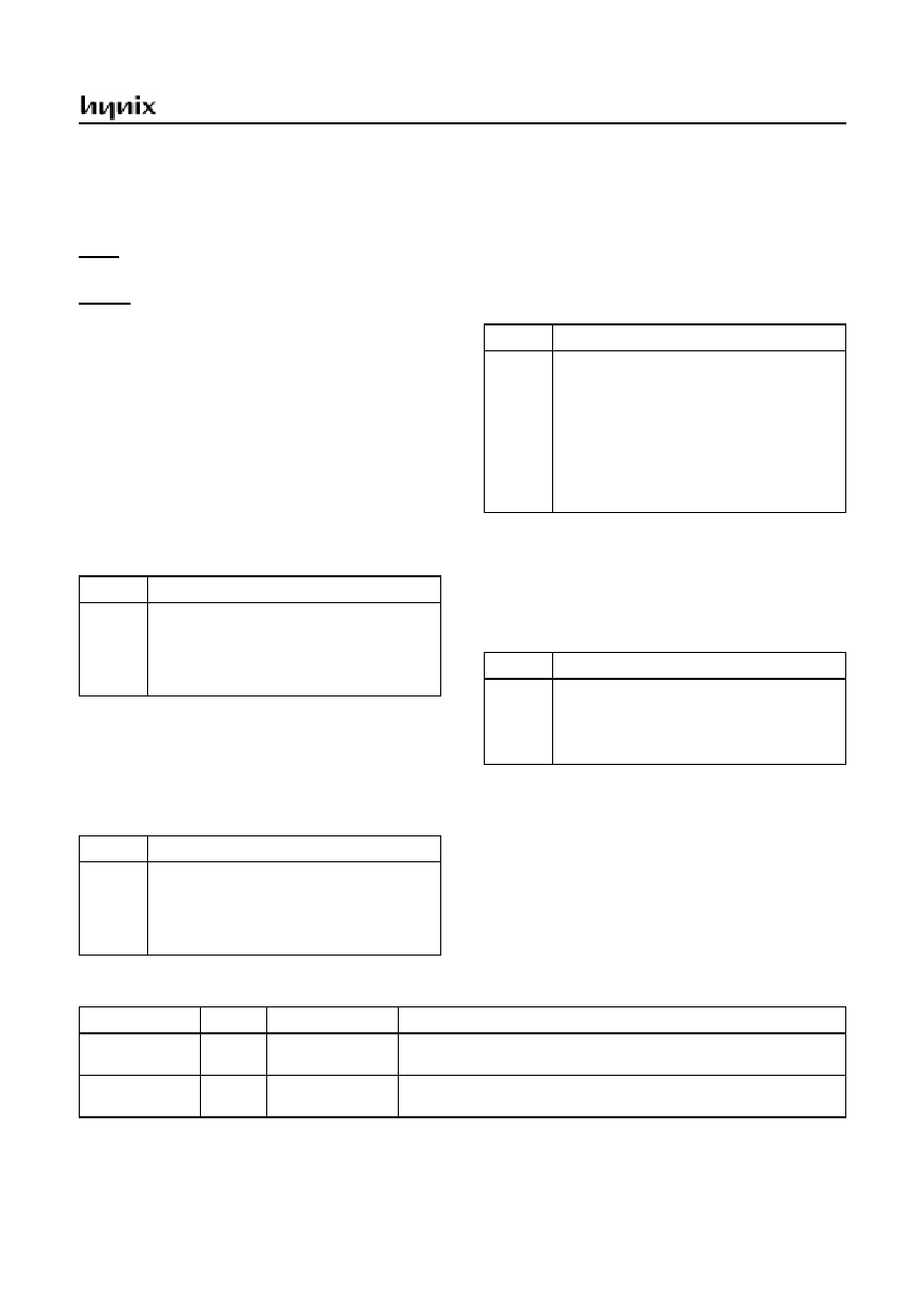
PIN NAME
Pin No.
In/Out
Function
V
DD
9,13,30,
37
-
Supply voltage
V
SS
14,29,
36,43
-
Circuit ground
Table 5-1 Port Function Description
HMS81C4x60
10
November 2001 Ver 1.1
TEST
44
I
TEST signal input (internal pull up resister)
RESET
33
I
Reset signal input
X
IN
35
I
Main oscillation input
X
OUT
34
O
Main oscillation output
HS
19
I
Horisontal Sync. input
VS
20
I
Vertical Sync. input
R
38
O
Red signal output
G
39
O
Green signal output
B
40
O
Blue signal output
YS
41
O
Edge signal output
YM
42
O
Background signal output
R30/PWM0
52
I/O
PWM functions
8bit PWM (pull up)
R31/PWM1
51
I/O
8bit PWM (pull up)
R32/PWM2
50
I/O
8bit PWM (pull up)
R33/PWM3
49
I/O
8bit PWM (pull up)
R34/PWM4
48
I/O
8bit PWM
R35/PWM5
47
I/O
14bit PWM
R36/BUZ
46
I/O
Buzzer (pull up)
R37/TMR1
45
I/O
Timer Interrupt 1
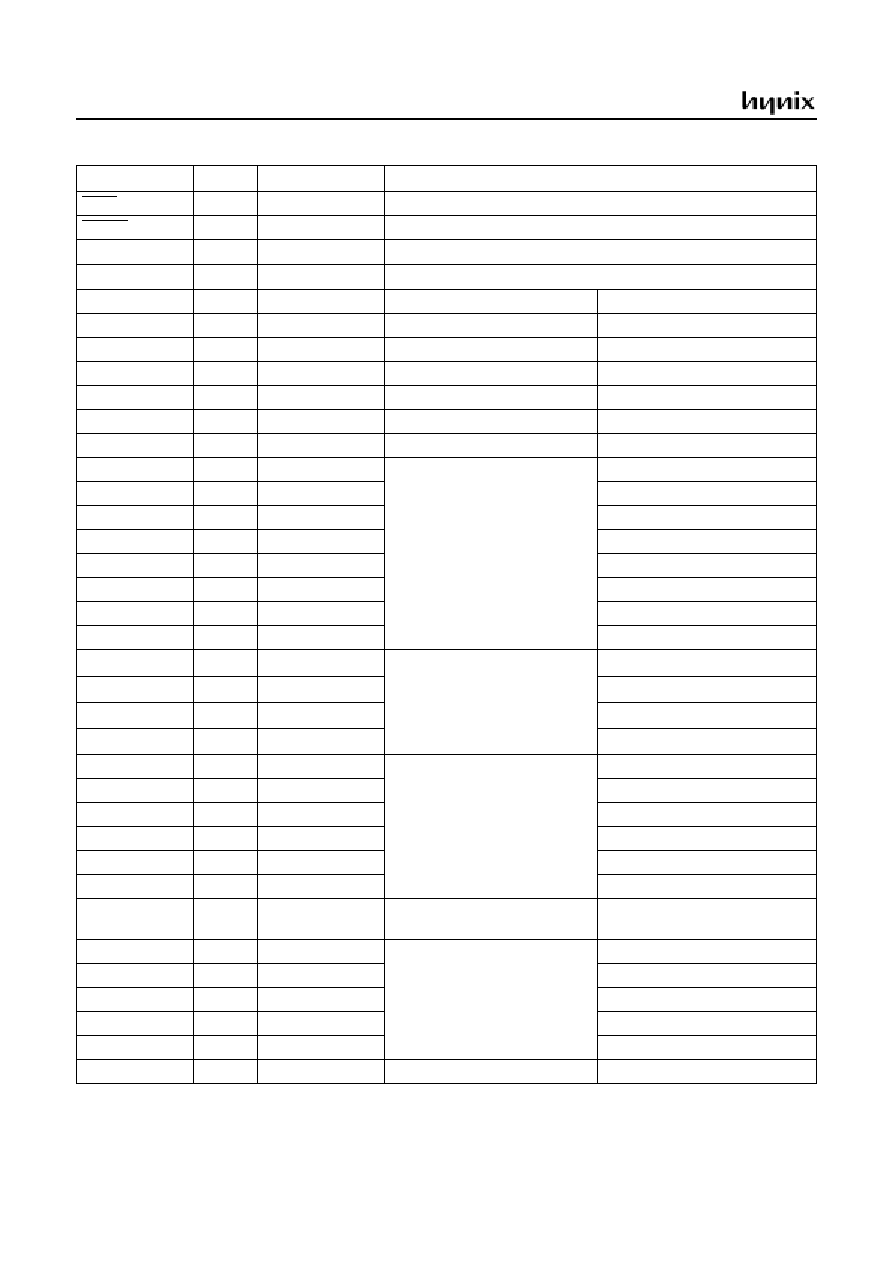
R40/SCL0
1
I/O
I
2
C functions (open drain)
I
2
C Serial clock 0
R41/SDA0
2
I/O
I
2
C Serial data 0
R42/SCL1
3
I/O
I
2
C Serial clock 1
R43/SDA1
4
I/O
I
2
C Serial data 1
R20
21
I/O
External interrupt functions
(pull up)
R21/INT1
22
I/O
External interrupt input 1
R22/INT2
23
I/O
External interrupt input 2 (pull up)
R23/INT3
24
I/O
External interrupt input 3
R24/EC2
25
I/O
Event counter input 2
R25/EC3
26
I/O
Event counter input 3 (pull up)
SCAP
11
I
Data slicer comparation reference
voltage
R10/AD0
15
I
A/D conversion functions
Analog input 0
R11/AD1
16
I
Analog input 1
R12/AD2
17
I
Analog input 2
R13/AD3
18
I
Analog input 3
R14/AD4
10
I
Analog input 4
CVBS
12
I
Composit video input
PIN NAME
Pin No.
In/Out
Function
Table 5-1 Port Function Description
HMS81C4x60
November 2001 Ver 1.1
11
R00
27
I/O
Digital I/O functions
(normal I/O, pull up)
R01
28
I/O
(normal I/O, pull up)
R02
31
I/O
(normal I/O)
R03
32
I/O
(normal I/O, pull up)
R04
5
I/O
(open drain, pull up)
R05
6
I/O
(open drain, pull up)
R06
7
I/O
(open drain, pull up)
R07
8
I/O
(open drain, pull up)
PIN NAME
Pin No.
In/Out
Function
Table 5-1 Port Function Description
HMS81C4x60
12
November 2001 Ver 1.1
6. PORT STRUCTURES
X
IN
, X
OUT
R03~R00,R37~R30,HS,VS,YS,YM
R14~10, CVBS
R07~R04, R43~R40, TEST
X
IN
X
OUT
V
SS
V
DD
V
SS
V
DD
Main frequency
clock
V
DD
V
SS
STOP
V
SS
Pin
V
DD
V
SS
V
DD
V
SS
I/O
Data out
Data in
Data in
Out Enable
Schmitt
€{
Pin
V
DD
V
SS
V
DD
V
SS
I
Data out
Data in
Data in
Out Enable
Schmitt
€{
Analog in
Analog in
Pin
Out Enable
V
SS
Data in
Data in
Data out
Schmitt
€{
I/O
V
DD
V
SS
HMS81C4x60
November 2001 Ver 1.1
13
R,G,B
R25~R20, RESET
SCAP
Pin
V
DD
V
SS
I/O
V
DD
V
SS
Pin
V
DD
V
SS
V
DD
V
SS
I/O
Data out
Data in
Data in
Out Enable
Schmitt
€{
Noise Filter
Pin
I/O
V
DD
V
SS
Data In
HMS81C4x60
14
November 2001 Ver 1.1
7. ELECTRICAL CHARACTERISTICS
7.1 Absolute Maximum Ratings
Supply voltage ........................................... -0.3 to +6.0 V
Storage Temperature ................................-40 to +125
∞
C
Voltage on any pin with respect to Ground (V
SS
)
............................................................... -0.3 to V
DD
+0.3
Maximum current out of Vss pin.........................160 mA
Maximum current into V
DD
pin ..........................160 mA
Maximum current sunk by(I
OL
per I/O Pin) .........20 mA
Maximum output current sourced by (I
OH
per I/O Pin)
.................................................................................8 mA
Maximum current (
I
OL
) .................................... 100 mA
Maximum current (
I
OH
)...................................... 80 mA
Note: Stresses above those listed under "Absolute Maxi-
mum Ratings" may cause permanent damage to the de-
vice. This is a stress rating only and functional operation of
the device at any other conditions above those indicated in
the operational sections of this specification is not implied.
Exposure to absolute maximum rating conditions for ex-
tended periods may affect device reliability.
7.2 Recommended Operating Conditions
7.3 DC Electrical Characteristics
(T
A
=-10~70
∞
C, V
DD
=4.5~5.5V)
,
Parameter
Symbol
Condition
Specifications
Unit
Min.
Max.
Supply Voltage
V
DD
V
DD
=4.5~5.5V
4.5
5.5
V
Operating Frequency
f
XIN
f
XIN
=4MHz
-
4.0(typical)
MHz
Operating Temperature
T
OPR
-10
70
∞
C
Parameter
Symbol
Condition
Specifications
Unit
Min.
Typ.
Max.
High level input voltage
V
IH
TEST, RESET, Xin, R0, R1, R2, R3,
HS, VS
0.8 V
DD
-
V
DD
V
Low level input voltage
V
IL
TEST, RESET, Xin, R0, R1, R2, R3,R4
HS, VS
0
-
0.12 V
DD
V
High level output voltage
V
OH
I
OH
= -5mA
R0, R1, R2, R3, YS, YM
V
DD
- 1
-
-
V
Low level output voltage
V
OL
I
OL
= 5mA
R0, R1, R2, R4
-
-
1.0
v
Supply current in
ACTIVE mode
I
DD
V
DD
-
40
80
mA
pull-up lekage current
I
RUP
V
DD
= 5.5v, V
PIN
= 0.4V
TEST, R00, R01, R03, R04, R05, R06,
R07, R20, R22, R25, R30, R31, R32, R33
R36
-1.5
-400
µ
A
High input leakage
current
I
IZH
V
DD
= 5.5V
,
V
PIN
= V
DD
All input, I/O pins except X
IN
-5
-
5
µ
A
HMS81C4x60
November 2001 Ver 1.1
15
7.4 AC Characteristics
(T
A
=-10~70
∞
C, V
DD
=5V
±
10%
,
V
SS
=0V)
Low input leakage
current
I
IZL
V
DD
= 5.5V
,
V
PIN
= 0V
All input, I/O pins except X
IN
, OSC1
-5
-
5
µ
A
RAM data retention
voltage
V
RAM
V
DD
1.2
-
-
V
Hysterisis
Vt+ ~
Vt-
TEST, RESET, Xin, HS, VS, R07 ~ R00,
R21, R23, R24, R25, R37 ~ R30
1.0
-
-
V
Comparator operating
range
V
rCVBS
V
DD
= 5V
CVBS pin
1.2
-
3.5
V
Comparator resolution
V
aCVBS
V
DD
= 5V
CVBS pin
-
-
0.08
V
RGB DAC
Resolution 1
RGB
R1
V
DD
= 5V
No in/out current in R,G,B pin
-
-
5
%
RGB DAC
Output voltage
V
RGB
RGB DAC On
No in/out current in R,G,B pin
V
Level 0
3/40V
dd
Level 1
5/40V
dd
Level 2
8/40V
dd
Level 3
12/40V
dd
Level 4
17/40V
dd
Level 5
23/40V
dd
Level 6
30/40V
dd
Level 7
38/40V
dd
RGB V
oh
V
ohrgb
V
DD
= 5V
RGB DAC On
Level 7
I
OH
= -3mA
3.1
3.5
3.9
V
RGB V
ol
V
olrgb
V
DD
= 5V
RGB DAC On
Level 0
I
OL
= 3mA
0.4
0.6
0.8
V
Parameter
Symbol
Condition
Specifications
Unit
Min.
Typ.
Max.
Parameter
Symbol
Pins
Specifications
Unit
Min.
Typ.
Max.
Crystal oscillator Frequency
f
XIN
X
IN
3
4
5
MHz
External Clock Pulse Width
t
MCPW
X
IN
180
-
350
nS
t
SCPW
S
CLK
0.5
-
µ
S
External Clock Transition Time
t
MRCP,
t
MFCP
X
IN
-
-
20
nS
t
SRCP,
t
SFCP
S
CLK
-
-
20
nS

HMS81C4x60
16
November 2001 Ver 1.1
Figure 7-1 Timing Chart
Oscillation Stabilizing Time
t
ST
X
IN
, X
OUT
-
-
20
mS
Interrupt Pulse Width
t
IW
INT1~3
2
-
-
t
SYS
1
RESET Input Width
t
RST
RESET
8
-
-
t
SYS
1
Event Counter Input Pulse
Width
t
ECW
EC2, EC3
2
-
-
t
SYS
1
Event Counter Transition Time
t
REC,
t
FEC
EC2, EC3
-
-
20
nS
1. t
SYS
is one of 1/f
XIN
main clock operation mode,
Parameter
Symbol
Pins
Specifications
Unit
Min.
Typ.
Max.
t
MRCP
t
MFCP
X
IN
INT1 ~ 3
0.5V
V
DD
-0.5V
0.2V
DD
0.8V
DD
0.2V
DD
RESET
t
REC
t
FEC
0.2V
DD
0.8V
DD
EC2, EC3
t
IW
t
IW
t
RST
t
ECW
t
ECW
1/f
XIN
t
MCPW
t
MCPW
HMS81C4x60
November 2001 Ver 1.1
17
7.5 A/D Converter Characteristics
(TA=25
∞
C, V
DD
=5V, V
SS
=0V)
Parameter
Symbol
Condition
Specifications
Unit
Min.
Typ.
Max.
Analog Input Voltage Range
V
AN
-
V
SS
-0.3
-
V
DD
+0.3
V
Overall Accuracy
CAIN
-
-
±
1.5
±
2.5
LSB
Non Linearity Error
NNLE
-
-
±
1.5
±
2.5
Differential Non Linearity Error
NDNLE
-
-
±
1.5
±
2.5
Zero Offset Error
NZOE
-
-
±
0.5
±
2.0
Full Scale Error
NFSE
-
-
±
0.75
±
1.0
Gain Error
NGE
-
-
±
1.5
±
2.0
Conversion Time
TCONV
f
MAIN
=4MHz
-
-
15
µ
S
HMS81C4x60
18
November 2001 Ver 1.1
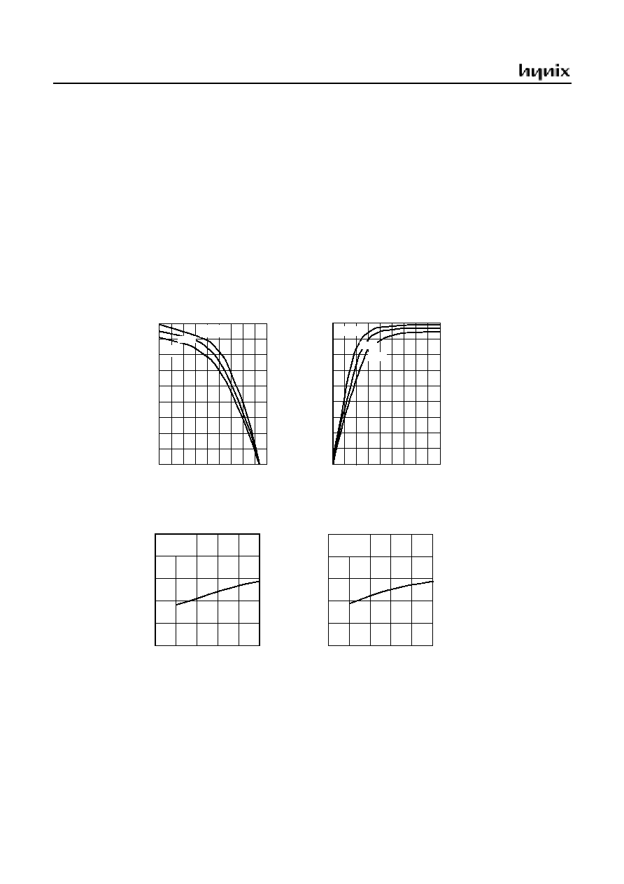
7.6 Typical Characteristics
These graphs and tables are for design guidance only and
are not tested or guaranteed.
In some graphs or tables, the datas presented are out-
side specified operating range (e.g. outside specified
V
DD
range). This is for information only and devices
are guaranteed to operate properly only within the
specified range.
The data is a statistical summary of data collected on units
from different lots over a period of time. "Typical" repre-
sents the mean of the distribution while "max" or "min"
represents (mean + 3
) and (mean
-
3
) respectively
where
is standard deviation
I
OL
-
V
OL
, V
DD
=5.2V
(mA)
I
OL
1.0
3.0
2.0
V
OL
(V)
I
OH
-
V
OH
, V
DD
=5.2V
-8
-6
-4
-2
0
(mA)
I
OH
2.0
3.0
V
OH
(V)
70
∞
C
f
MAIN
=4MHz
V
DD
-
V
IH
4
3
2
1
0
(V)
V
IH1
4
4.5
5
5.5
6
V
DD
(V)
Ta=25
∞
C
40
30
10
-10
-12
-14
4.0
20
f
MAIN
=4MHz
V
DD
-
V
IH
4
3
2
1
0
(V)
V
IH2
4
4.5
5
5.5
6
V
DD
(V)
Ta=25
∞
C
Hysterisis
-16
5.0
25
∞
C
-20
∞
C
4.0
-20
∞
C
70
∞
C
25
∞
C
HMS81C4x60
November 2001 Ver 1.1
19
Ta= -20~70
∞
C
(Main-clock)
Ta=25
∞
C
I
DD1
-
V
DD
60
50
40
30
20
(mA)
I
DD
4
4.5
5
5.5
6
V
DD
(V)
Normal Mode (Main opr.)
6
4
2
1
0
(MHz)
f
MAIN
4
4.5
5
5.5
6.5
V
DD
(V)
Operating Area
f
MAIN
=4MHz
5
3
6
f
MAIN
=4MHz
V
DD
-
V
IL
3
2
1
(V)
V
IL1
4
4.5
5
5.5
6
V
DD
(V)
Ta=25
∞
C
Hysterisis
f
MAIN
=4MHz
V
DD
-
V
IL
3
2
1
(V)
V
IL1
4
4.5
5
5.5
6
V
DD
(V)
Ta=25
∞
C
HMS81C4x60
20
November 2001 Ver 1.1
8. MEMORY ORGANIZATION
The GMS81C4x60 has separate address spaces for Pro-
gram memory, Data Memory and Display memory. Pro-
gram memory can only be read, not written to. It can be up
to 60K bytes of Program memory. Data memory can be
read and written to up to 1024 bytes including the stack ar-
ea. Font memory has prepared 32K bytes for OSD.
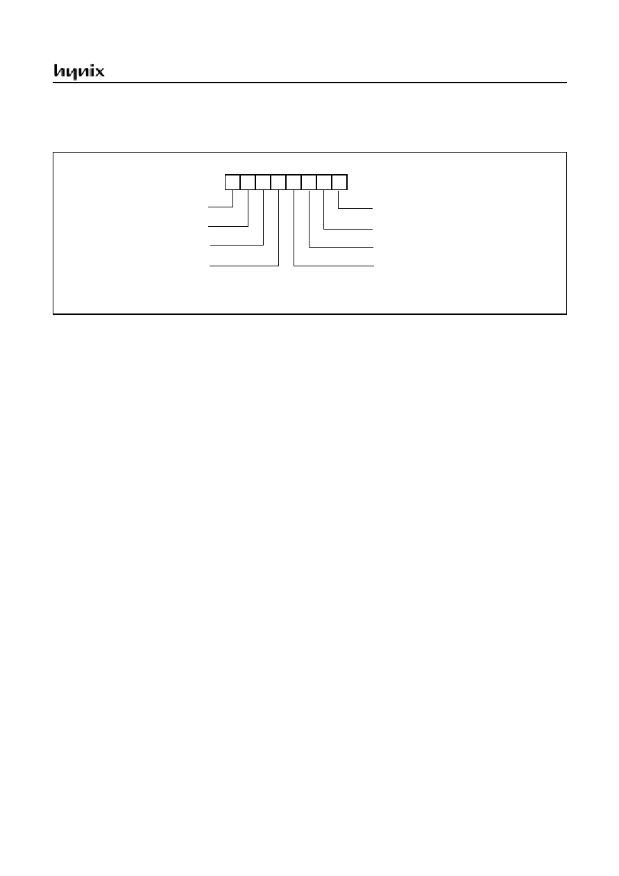
8.1 Registers
This device has six registers that are the Program Counter
(PC), a Accumulator (A), two index registers (X, Y), the
Stack Pointer (SP), and the Program Status Word (PSW).
The Program Counter consists of 16-bit register.
Figure 8-1 Configuration of Registers
Accumulator: The Accumulator is the 8-bit general pur-
pose register, used for data operation such as transfer, tem-
porary saving, and conditional judgement, etc.
The Accumulator can be used as a 16-bit register with Y
Register as shown below.
Figure 8-2 Configuration of YA 16-bit Register
X, Y Registers: In the addressing mode which uses these
index registers, the register contents are added to the spec-
ified address, which becomes the actual address. These
modes are extremely effective for referencing subroutine
tables and memory tables. The index registers also have in-
crement, decrement, comparison and data transfer func-
tions, and they can be used as simple accumulators.
Stack Pointer: The Stack Pointer is an 8-bit register used
for occurrence interrupts and calling out subroutines. Stack
Pointer identifies the location in the stack to be accessed
(save or restore).
Generally, SP is automatically updated when a subroutine
call is executed or an interrupt is accepted. However, if it
is used in excess of the stack area permitted by the data
memory allocating configuration, the user-processed data
may be lost.
The stack can be located at any position within 00
H
to FF
H
of the internal data memory. The SP is not initialized by
hardware, requiring to write the initial value (the location
with which the use of the stack starts) by using the initial-
ization routine. Normally, the initial value of "FF
H"
is
used.
Program Counter: The Program Counter is a 16-bit wide
which consists of two 8-bit registers, PCH and PCL. This
counter indicates the address of the next instruction to be
executed. In reset state, the program counter has reset rou-
tine address (PC
H
:0FF
H
, PC
L
:0FE
H
).
Program Status Word: The Program Status Word (PSW)
contains several bits that reflect the current state of the
CPU. The PSW is described in Figure 8-3. It contains the
Negative flag, the Overflow flag, the Break flag the Half
Carry (for BCD operation), the Interrupt enable flag, the
Zero flag, and the Carry flag.
[Carry flag C]
This flag stores any carry or borrow from the ALU of CPU
after an arithmetic operation and is also changed by the
Shift Instruction or Rotate Instruction.
A
ACCUMULATOR
X REGISTER
Y REGISTER
STACK POINTER
PROGRAM COUNTER
PROGRAM STATUS
WORD
X
Y
SP
PCL
PCH
PSW
Two 8-bit Registers can be used as a "YA" 16-bit Register
Y
A
Y
A
Caution:
The Stack Pointer must be initialized by software be-
cause its value is undefined after RESET.
Example: To initialize the SP
LDX
#0FFH
TXSP
; SP
FF
H
SP
1
Stack Address (00
H
~ FF
H
)
15
0
8
7
Hardware fixed
HMS81C4x60
November 2001 Ver 1.1
21
[Zero flag Z]
This flag is set when the result of an arithmetic operation
or data transfer is "0" and is cleared by any other result.
Figure 8-3 PSW (Program Status Word) Register
[Interrupt disable flag I]
This flag enables/disables all interrupts except interrupt
caused by Reset or software BRK instruction. All inter-
rupts are disabled when cleared to "0". This flag immedi-
ately becomes "0" when an interrupt is served. It is set by
the EI instruction and cleared by the DI instruction.
[Half carry flag H]
After operation, this is set when there is a carry from bit 3
of ALU or there is no borrow from bit 4 of ALU. This bit
can not be set or cleared except CLRV instruction with
Overflow flag (V).
[Break flag B]
This flag is set by software BRK instruction to distinguish
BRK from TCALL instruction with the same vector ad-
dress.
[Direct page flag G]
This flag assigns RAM page for direct addressing mode. In
the direct addressing mode, addressing area is from zero
page 00
H
to 0FF
H
when this flag is "0". If it is set to "1",
addressing area is assigned by RPR register (address
0F3
H
). It is set by SETG instruction and cleared by CLRG.
[Overflow flag V]
This flag is set to "1" when an overflow occurs as the result
of an arithmetic operation involving signs. An overflow
occurs when the result of an addition or subtraction ex-
ceeds
+
127 (7F
H
) or
-
128 (80
H
). The CLRV instruction
clears the overflow flag. There is no set instruction. When
the BIT instruction is executed, bit 6 of memory is copied
to this flag.
[Negative flag N]
This flag is set to match the sign bit (bit 7) status of the re-
sult of a data or arithmetic operation. When the BIT in-
struction is executed, bit 7 of memory is copied to this flag.
N
NEGATIVE FLAG
V
G
B
H
I
Z
C
MSB
LSB
RESET VALUE : 00
H
PSW
OVERFLOW FLAG
BRK FLAG
CARRY FLAG RECEIVES
ZERO FLAG
INTERRUPT ENABLE FLAG
CARRY OUT
HALF CARRY FLAG RECEIVES
CARRY OUT FROM BIT 1 OF
ADDITION OPERLANDS
SELECT DIRECT PAGE
when g=1, page is addressed by RPR
HMS81C4x60
22
November 2001 Ver 1.1
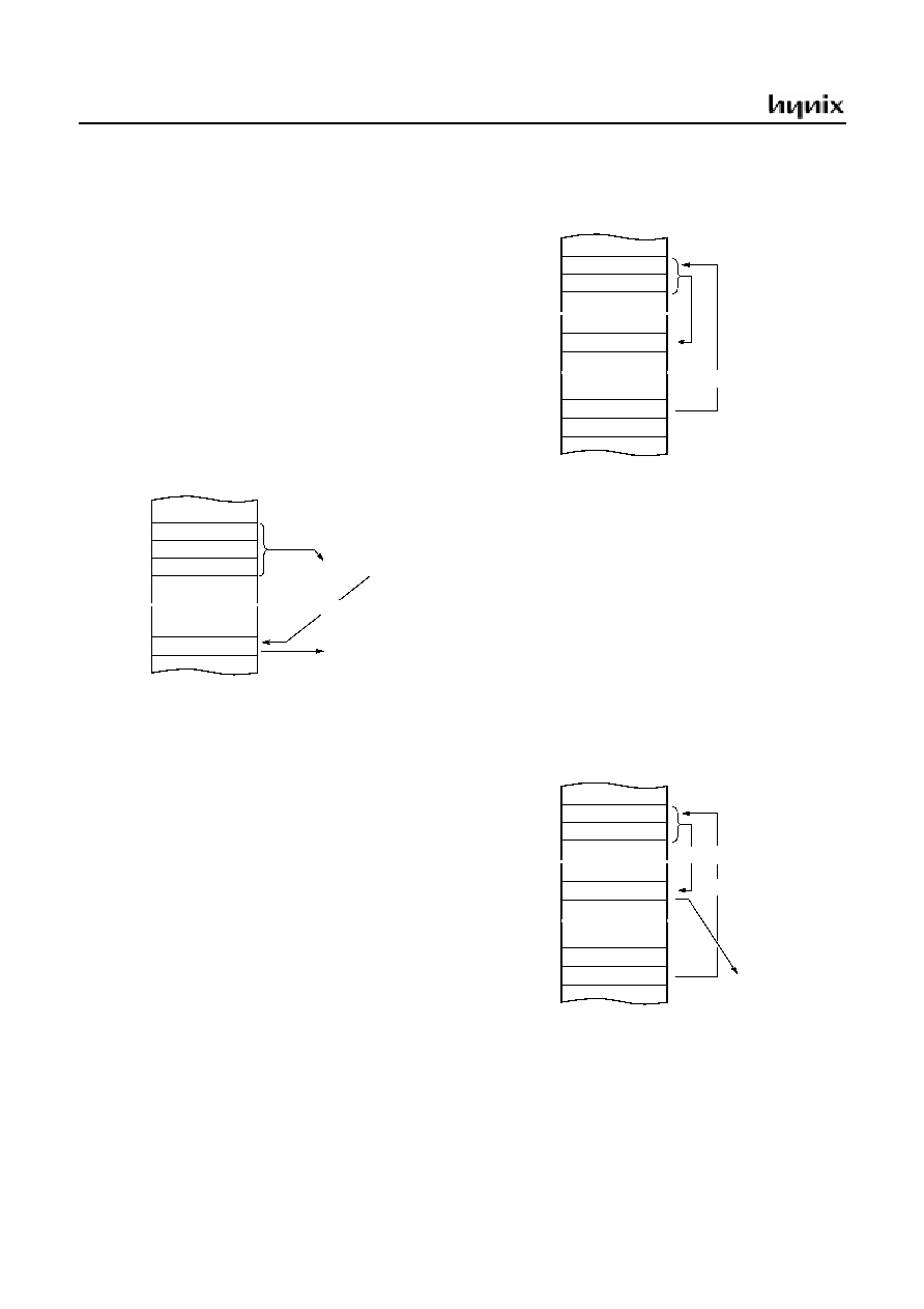
Figure 8-4 Stack Operation
At execution of a
CALL/TCALL/PCALL
PCL
PCH
01BF
SP after
execution
SP before
execution
01BD
01BE
01BD
01BC
01BF
Push
down
At acceptance
of interrupt
PCL
PCH
01BF
01BC
01BE
01BD
01BC
01BF
Push
down
PSW
At execution
of RET instruction
PCL
PCH
01BF
01BF
01BE
01BD
01BC
01BD
Pop
up
At execution
of RETI instruction
PCL
PCH
01BF
01BF
01BE
01BD
01BC
01BC
Pop
up
PSW
0100
H
01BF
H
Stack
depth
At execution
of PUSH instruction
A
01BF
01BE
01BE
01BD
01BC
01BF
Push
down
SP after
execution
SP before
execution
PUSH A (X,Y,PSW)
At execution
of POP instruction
A
01BF
01BF
01BE
01BD
01BC
01BE
Pop
up
POP A (X,Y,PSW)
HMS81C4x60
November 2001 Ver 1.1
23
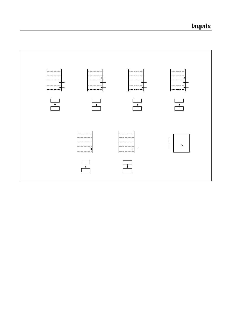
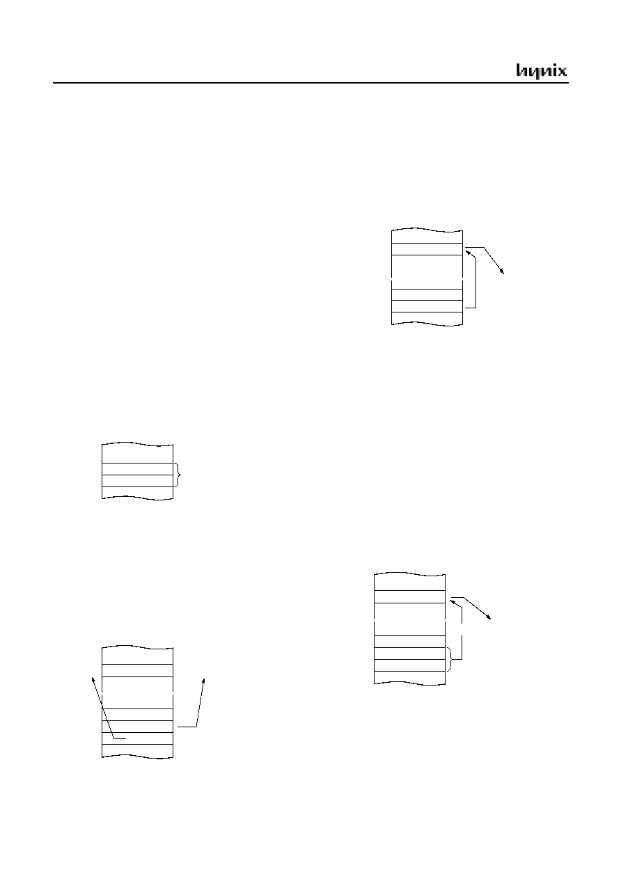
8.2 Program Memory
A 16-bit program counter is capable of addressing up to
64K bytes, but this device has 60K bytes program memory
space only physically implemented. Accessing a location
above FFFF
H
will cause a wrap-around to 0000
H
.
Figure 8-5 shows a map of Program Memory. After reset,
the CPU begins execution from reset vector which is stored
in address FFFE
H
and FFFF
H
as shown in Figure 8-6.
As shown in Figure 8-5, each area is assigned a fixed loca-
tion in Program Memory. Program Memory area contains
the user program.
Figure 8-5 Program Memory Map
Page Call (PCALL) area contains subroutine program to
reduce program byte length by using 2 bytes PCALL in-
stead of 3 bytes CALL instruction. If it is frequently called,
it is more useful to save program byte length.
Table Call (TCALL) causes the CPU to jump to each
TCALL address, where it commences the execution of the
service routine. The Table Call service area spaces 2-byte
for every TCALL: 0FFC0
H
for TCALL15, 0FFC2
H
for
TCALL14, etc., as shown in Figure 8-7.
Example: Usage of TCALL
The interrupt causes the CPU to jump to specific location,
where it commences the execution of the service routine.
The External interrupt 1, for example, is assigned to loca-
tion 0FFF8
H
. The interrupt service locations spaces 2-byte
interval: 0FFF6
H
and 0FFF7
H
for External Interrupt 2,
0FFE8
H
and 0FFE9
H
for External Interrupt 3, etc.
Any area from 0FF00
H
to 0FFFF
H
, if it is not going to be
used, its service location is available as general purpose
Program Memory.
Figure 8-6 Interrupt Vector Area
PROGRAM
MEMORY
TCALL
AREA
INTERRUPT
VECTOR AREA
1000
H
FEFF
H
FF00
H
FFC0
H
FFDF
H
FFE0
H
FFFF
H
PCALL
AREA
LDA
#5
TCALL
15
;1BYTE INSTRUCTION
:
;INSTEAD OF 2 BYTES
:
;NORMAL CALL
;
;TABLE CALL ROUTINE
;
FUNC_A:
LDA
LRG0
RET
;
FUNC_B:
LDA
LRG1
RET
;
;TABLE CALL ADD. AREA
;
ORG
0FFC0H
;TCALL ADDRESS AREA
DW
FUNC_A
DW
FUNC_B
1
2
0FFE0
H
E2
Address
Vector Area Memory
E4
E6
E8
EA
EC
EE
F0
F2
F4
F6
F8
FA
FC
FE
I
2
C Bus Interface Interrupt Vector
-
Basic Interval Timer Interrupt Vector
Watchdog Timer Interrupt Vector
Timer/Counter 3 Interrupt Vector
Timer/Counter 1 Interrupt Vector
V-Sync Interrupt Vector
Timer/Counter 2 Interrupt Vector
Timer/Counter 0 Interrupt Vector
External Interrupt 2 Vector
On Screen Display Interrupt Vector
-
RESET Vector
External Interrupt 1 Vector
Slicer Interrupt Vector
External Interrupt 3/4 Vector
"-" means reserved area.
NOTE:
HMS81C4x60
24
November 2001 Ver 1.1
Figure 8-7 PCALL and TCALL Memory Area
PCALL
rel
4F35
PCALL 35
H
TCALL
n
4A
TCALL
4
0FFC0
H
C1
Address
Program Memory
C2
C3
C4
C5
C6
C7
C8
0FF00
H
Address
PCALL Area Memory
0FFFF
H
PCALL Area
(256 Bytes)
* means that the BRK software interrupt is using
same address with TCALL0.
NOTE:
TCALL 15
TCALL 14
TCALL 13
TCALL 12
TCALL 11
TCALL 10
TCALL 9
TCALL 8
TCALL 7
TCALL 6
TCALL 5
TCALL 4
TCALL 3
TCALL 2
TCALL 1
TCALL 0 / BRK *
C9
CA
CB
CC
CD
CE
CF
D0
D1
D2
D3
D4
D5
D6
D7
D8
D9
DA
DB
DC
DD
DE
DF
4F
~
~
~
~
NEXT
35
0FF35
H
0FF00
H
0FFFF
H
11111111 11010110
01001010
PC:
F
H
F
H
D
H
6
H
4A
~
~
~
~
25
0FFD6
H
0FF00
H
0FFFF
H
D1
NEXT
0FFD7
H
¿
√
0D125
H
Reverse
√ : index address

HMS81C4x60
November 2001 Ver 1.1
25
Example: The usage software example of Vector address and the initialize part.
ORG
0FFE0H
DW
I2C_INT
DW
NOT_USED
DW
BIT_INT
DW
WDT_INT
DW
IR_INT
DW
TIMER3
DW
TIMER1
DW
VSYNC_INT
DW
SLICE_INT
DW
T2_INT
DW
T0_INT
DW
EXT2_INT
DW
EXT1_INT
DW
OSD_INT
DW
NOT_USED
DW
RESET
ORG
0F000H
;********************************************
;
MAIN PROGRAM *
;********************************************
;
RESET:
DI
;Disable All Interrupts
CLRG
LDX
#0
RAM_CLR:
LDA
#0
;RAM Clear(!0000
H
->!00BF
H
)
STA
{X}+
CMPX
#0C0H
BNE
RAM_CLR
;
LDX
#0FFH
;Stack Pointer Initialize
TXSP
;
LDM
PLLC,#0000_0101b
;16MHz system clock
;
LDM
R0, #0FFh
;Normal Port 0
LDM
R0DIR,#0FFh
;Normal Port Direction
:
:
LDM
TM0,#0000_0000B
;timer stop
:
:
CALL
VRAM_CLR
;Clear VRAM
:
:

HMS81C4x60
26
November 2001 Ver 1.1
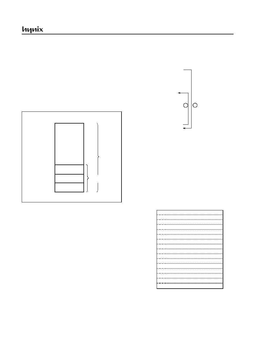
8.3 Data Memory
Figure 8-8 shows the internal Data Memory space availa-
ble. Data Memory is divided into four groups, a user RAM,
control registers, Stack, and OSD memory.
Figure 8-8 Data Memory Map
User Memory
The GMS81C4x60 has 1,024
◊
8 bits for the user memory
(RAM) except Peripheral Reg. (64 bytes) .
Control Registers
The control registers are used by the CPU and Peripheral
function blocks for controlling the desired operation of the
device. Therefore these registers contain control and status
bits for the interrupt system, the timer/ counters, analog to
digital converters and I/O ports. The control registers are in
address range of 0C0
H
to 0FF
H
.
Note that unoccupied addresses may not be implemented
on the chip. Read accesses to these addresses will in gen-
eral return random data, and write accesses will have an in-
determinate effect.
More detailed informations of each register are explained
in each peripheral section.
Note: Write only registers can not be accessed by bit ma-
nipulation instruction. Do not use read-modify-write instruc-
tion. Use byte manipulation instruction.
Example; To write at CKCTLR
LDM
CKCTLR,#05H ;Divide ratio
˜
8
Stack Area
The stack provides the area where the return address is
saved before a jump is performed during the processing
routine at the execution of a subroutine call instruction or
the acceptance of an interrupt.
When returning from the processing routine, executing the
subroutine return instruction [RET] restores the contents of
the program counter from the stack; executing the interrupt
return instruction [RETI] restores the contents of the pro-
gram counter and flags.
The save/restore locations in the stack are determined by
the stack pointed (SP). The SP is automatically decreased
after the saving, and increased before the restoring. This
means the value of the SP indicates the stack location
number for the next save. Refer to Figure 8-4 on page 22.
Page0
RAM (192 bytes)
Peripheral Reg. (64 bytes)
0100H
00C0H
0000H
RAM (256 bytes)
0200H
RAM (256 bytes)
0300H
RAM (256 bytes)
0400H
0500H
0600H
RAM (64 bytes)
0A00H
OSD RAM (192 bytes)
0AC0H
Peripheral Reg. (32 bytes)
Page1
Page2
Page3
Page4
Page5
Page6
PageA
Stack area
NOT USED
RAM (Slicer RAM)
( 256 Byte)
0B00H
OSD RAM (192 bytes)
0BC0H Peripheral Reg. (32 bytes)
PageB
NOT USED
0C00H
0FFFH
Not Used
0700H
NOT USED
0440H
Address
Symbol
R/W
Reset Value
Addressin
g mode
00C0H
00C1H
00C2H
00C3H
00C4H
00C5H
00C6H
00C7H
00C8H
00C9H
00CAH
00CBH
00CCH
00CDH
00CEH
00CFH
R0
R0DD
R1
R1DD
R2
R2DD
R3
R3DD
R4
R4DD
reserved
reserved
reserved
reserved
FUNC
PLLC
R/W
W
R
W
R/W
W
R/W
W
R/W
W
-
-
-
-
W
W
????????
00000000
????????
---00000
????????
--000000
????????
00000000
????????
----0000
-
-
-
-
0000000-
-0000000
byte, bit
1
byte
2
byte, bit
byte
byte, bit
byte
byte, bit
byte
byte, bit
byte
-
-
-
-
byte
byte
Table 8-1Control registers

HMS81C4x60
November 2001 Ver 1.1
27
0D0H
0D1H
0D2H
0D3H
0D4H
0D5H
0D6H
0D6H
0D7H
0D8H
0D9H
0DAH
0DBH
0DCH
0DEH
0DFH
TM0
TM2
TDR0
TDR1
TDR2
TDR3
BITR
CKCTLR
WDTR
ICAR
ICDR
ICSR
ICCR
reserved
reserved
reserved
R/W
R/W
R/W
R/W
R/W
R/W
R
W
W
R/W
R/W
R/W
R/W
-
-
-
-0000000
-0000000
????????
????????
????????
????????
????????
--010111
-0111111
00000000
11111111
0001000-
00000000
-
-
-
byte
byte
byte, bit
byte, bit
byte, bit
byte, bit
byte
byte
byte
byte, bit
byte, bit
byte, bit
byte, bit
-
-
-
0E0H
0E1H
0E2H
0E3H
0E4H
0E5H
0E6H
0E7H
0E8H
0E9H
0EAH
0EBH
0ECH
0EDH
0EEH
0EFH
PWMR0
PWMR1
PWMR2
PWMR3
PWMR4
PWMR5H
PWMR5L
reserved
reserved
reserved
PWMCR1
PWMCR2
reserved
reserved
reserved
AIPS
W
W
W
W
W
R/W
R/W
-
-
-
R/W
R/W
-
-
-
W
????????
????????
????????
????????
????????
????????
--??????
-
-
-
00000000
-----000
-
-
-
--000000
byte
byte
byte
byte
byte
byte
byte, bit
-
-
-
byte, bit
byte, bit
-
-
-
byte
0F0H
0F1H
0F2H
0F3H
0F4H
0F5H
0F6H
0F7H
0F8H
0F9H
0FAH
0FBH
0FCH
0FDH
0FEH
0FFH
ADCM
ADR
IEDS
IMOD
IENL
IRQL
IENH
IRQH
reversed
IDCR
IDFS
IDR
DPGR
TMR
reserved
reserved
R/W
R
W
R/W
R/W
R/W
R/W
R/W
-
R/W
R
R
R/W
W
-
-
????????
????????
--000000
--000000
00000000
00000000
00000000
00000000
-
0000-000
1----001
????????
----0000
????????
-
-
byte, bit
byte
byte
byte, bit
byte, bit
byte, bit
byte, bit
byte, bit
-
byte, bit
byte
byte
byte, bit
byte
-
-
Table 8-1Control registers
0AD0
0AD1
0AD2
0AD3
0AD4
0AD5
0AD6
0AD7
0AD8
0AD9
0ADA
0ADB
0ADC
0ADD
0ADE
0ADF
RED0
RED1
RED2
GREEN0
GREEN1
GREEN2
BLUE0
BLUE1
BLUE2
reserved
reserved
reserved
reserved
reserved
reserved
reserved
W
W
W
W
W
W
W
W
W
-
-
-
-
-
-
-
????????
????????
????????
????????
????????
????????
????????
????????
????????
-
-
-
-
-
-
-
byte, bit-
byte, bit
byte, bit
byte, bit
byte, bit
byte, bit
byte, bit
byte, bit
byte, bit
-
-
-
-
-
-
-
0AE0H
0AE1H
0AE2H
0AE3H
0AE4H
0AE5H
0AE6H
0AE7H
0AE8H
0AE9H
0AEAH
0AEBH
0AECH
0AEDH
0AEEH
0AEFH
0AF0H
0AF1H
0AF2H
0AF3H
0AF4H
0AF5H
0AF9H
OSDCON1
OSDCON2
OSDCON3
FDWSET
EDGECOL
CHEDCL
OSDLN
LHPOS
DLLMOD
DLLTST
L1ATTR
L1EATR
L1VPOS
L2ATTR
L2EATR
L2VPOS
WINSH
WINSY
WINEH
WINEY
VCNT
HCNT
CULTAD
R/W
R/W
W
W
W
W
R
W
W
R
W
W
W
W
W
W
W
W
W
W
R
R
W
00000000
00000000
00000000
01111010
10000111
????????
---00000
????????
00000000
--000000
??????-?
---?????
????????
????????
---?????
????????
????????
????????
????????
????????
????????
????????
????????
byte, bit
byte, bit
byte, bit
byte
byte
byte
byte
byte
byte
byte
byte, bit
byte, bit
byte
byte, bit
byte, bit
byte, bit
byte
byte
byte
byte
byte
byte
byte
0BE0H
0BE1H
0BE2H
0BE3H
0BE4H
0BE7H
0BE8H
SLCON
SLINF0
SLINF1
RIKST
RIKED
SNCST
SNCED
R/W
W
W
W
W
W
W
00000000
00000000
00000000
????????
????????
????????
????????
byte, bit
byte, bit
byte, bit
byte
byte
byte
byte
1. "byte, bit" means that register can be addressed by not only bit
but byte manipulation instruction.
2. "byte" means that register can be addressed by only byte
manipulation instruction. On the other hand, do not use any
read-modify-write instruction such as bit manipulation for clear-
ing bit.
Table 8-1Control registers
HMS81C4x60
28
November 2001 Ver 1.1
8.4 Addressing Mode
The GMS81C4x60 uses six addressing modes;
∑ Register addressing
∑ Immediate addressing
∑ Direct page addressing
∑ Absolute addressing
∑ Indexed addressing
∑ Register-indirect addressing
(1) Register Addressing
Register addressing accesses the A, X, Y, C and PSW.
(2) Immediate Addressing
#imm
In this mode, second byte (operand) is accessed as a data
immediately.
Example:
FE0435
ADC
#35
H
When G-flag is 1, then RAM address is defined by 16-bit
address which is composed of 8-bit RAM paging register
(RPR) and 8-bit immediate data.
Example: G=1, RPR=01
H
E45535
LDM
35
H
,#55
H
(3) Direct Page Addressing
dp
In this mode, a address is specified within direct page.
Example; G=0
E551: C535 LDA 35
H
;A
RAM[35
H
]
(4) Absolute Addressing
!abs
Absolute addressing sets corresponding memory data to
Data, i.e. second byte (Operand I) of command becomes
lower level address and third byte (Operand II) becomes
upper level address.
With 3 bytes command, it is possible to access to whole
memory area.
ADC, AND, CMP, CMPX, CMPY, EOR, LDA, LDX,
LDY, OR, SBC, STA, STX, STY
Example;
F100: 0735F0 ADC !0F035
H
;A
ROM[0F035
H
]
35
A+35
H
+C
A
04
MEMORY
E4
0F100
H
data
55
H
~
~
~
~
data
0135
H
˛
35
0F102
H
55
0F101
H
¿
data
35
35
H
0E551
H
data
A
¿
˛
~
~
~
~
C5
0E550
H
˛ : direct page
07
0F100
H
~
~
~
~
data
0F035
H
˛
F0
0F102
H
35
0F101
H
¿
A+data+C
A
address: 0F035
HMS81C4x60
November 2001 Ver 1.1
29
The operation within data memory (RAM)
ASL, BIT, DEC, INC, LSR, ROL, ROR
Example; Addressing accesses the address 0135
H
regard-
less of G-flag and RPR.
F100: 981501 INC !0115
H
;A
ROM[115
H
]
(5) Indexed Addressing
X indexed direct page (no offset)
{X}
In this mode, a address is specified by the X register.
ADC, AND, CMP, EOR, LDA, OR, SBC, STA, XMA
Example; X=15
H
, G=1, RPR=01
H
E550: D4 LDA
{X}
;ACC
RAM[X].
X indexed direct page, auto increment
{X}+
In this mode, a address is specified within direct page by
the X register and the content of X is increased by 1.
LDA, STA
Example; G=0, X=35
H
F100: DB LDA
{X}+
X indexed direct page (8 bit offset)
dp+X
This address value is the second byte (Operand) of com-
mand plus the data of
-register. And it assigns the mem-
ory in Direct page.
ADC, AND, CMP, EOR, LDA, LDY, OR, SBC, STA
STY, XMA, ASL, DEC, INC, LSR, ROL, ROR
Example; G=0, X=0F5
H
E550: C645 LDA 45
H
+X
98
0F100
H
~
~
~
~
data
115
H
˛
01
0F102
H
15
0F101
H
¿
data+1
data
√
address: 0115
data
D4
115
H
0E550
H
data
A
¿
˛
~
~
~
~
data
DB
35
H
data
A
¿
˛
~
~
~
~
36H
X
data
45
3A
H
0E551
H
data
A
¿
˛
~
~
~
~
C6
0E550
H
45
H
+0F5
H
=13A
H
√
HMS81C4x60
30
November 2001 Ver 1.1
Y indexed direct page (8 bit offset)
dp+Y
This address value is the second byte (Operand) of com-
mand plus the data of Y-register, which assigns Memory in
Direct page.
This is same with above (2). Use Y register instead of X.
Y indexed absolute
!abs+Y
Sets the value of 16-bit absolute address plus Y-register
data as Memory. This addressing mode can specify mem-
ory in whole area.
Example; Y=55
H
F100: D500FA LDA !0FA00
H
+Y
(6) Indirect Addressing
Direct page indirect
[dp]
Assigns data address to use for accomplishing command
which sets memory data (or pair memory) by Operand.
Also index can be used with Index register X,Y.
JMP, CALL
Example; G=0
FA00: 3F35 JMP [35
H
]
X indexed indirect
[dp+X]
Processes memory data as Data, assigned by 16-bit pair
m e m o r y w h i c h i s d e t e r m i n e d b y p a i r d a t a
[dp+X+1][dp+X] Operand plus X-register data in Direct
page.
ADC, AND, CMP, EOR, LDA, OR, SBC, STA
Example; G=0, X=10
H
FA00: 1625 ADC [25
H
+X]
D5
0F100
H
data
A
˛
~
~
~
~
data
0FA55
H
0FA00
H
+55
H
=0FA55
H
√
FA
0F102
H
00
0F101
H
¿
0A
35
H
jump to address 0E30A
H
˛
~
~
~
~
35
0FA00
H
E3
36
H
¿
3F
0E30A
H
NEXT
~
~
~
~
05
35
H
0E005
H
~
~
~
~
25
0FA00
H
E0
36
H
16
0E005
H
data
~
~
~
~
√
A + data + C
A
25 + X(10) = 35
H
˛
¿

HMS81C4x60
November 2001 Ver 1.1
31
Y indexed indirect
[dp]+Y
Processes memory data as Data, assigned by the data
[dp+1][dp] of 16-bit pair memory paired by Operand in Di-
rect page plus Y-register data.
ADC, AND, CMP, EOR, LDA, OR, SBC, STA
Example; G=0, Y=10
H
FA00: 1725 ADC [25
H
]+Y
Absolute indirect
[!abs]
The program jumps to address specified by 16-bit absolute
address.
JMP
Example; G=0
FA00: 1F25E0 JMP [!0E025
H
]
05
25
H
0E005
H
+ Y(10) = 0E015
H
˛
~
~
~
~
25
0FA00
H
E0
26
H
¿
17
0E015
H
data
~
~
~
~
√
A + data + C
A
25
0E025
H
jump to
~
~
~
~
E0
0FA00
H
E7
0E026
H
¿
25
0E725
H
NEXT
~
~
~
~
1F
PROGRAM MEMORY
˛
address 0E725
H

HMS81C4x60
32
November 2001 Ver 1.1
9. I/O PORTS
The HMS81C4x60 has 5 ports (R0, R1, R2, R3 and R4)
and OSD ports (R,G,B,YS,YM). These ports pins may be
multiplexed with an alternatefunction for the peripheral
features on the device. In general, in an initial reset state,
R ports are used as a general purpose digital port.
9.1 Registers for Port
Port Data Registers
The Port Data Registers (R0, R1, R2, R3, R4) are repre-
sented as a D-Type flip-flop, which will clock in a value
from the internal bus in response to a "write to data regis-
ter" signal from the CPU. The Q output of the flip-flop is
placed on the internal bus in response to a "read data reg-
ister" signal from the CPU. The level of the port pin itself
is placed on the internal bus in response to "read data reg-
ister" signal from the CPU. Some instructions that read a
port activating the "read register" signal, and others acti-
vating the "read pin" signal.
Port Direction Registers
All pins have data direction registers which can define
these ports as output or input. A "1" in the port direction
register configure the corresponding port pin as output.
Conversely, write "0" to the corresponding bit to specify it
as input pin. For example, to use the even numbered bit of
R0 as output ports and the odd numbered bits as input
ports, write "55
H
" to address 0C1
H
(R0 port direction reg-
ister) during initial setting as shown in Figure 9-1.
All the port direction registers in the HMS81C4x60 have
been written to zero by reset function. On the other hand,
its initial status is input.
Figure 9-1 Example of port I/O assignment
I : INPUT PORT
WRITE "55
H
" TO PORT R0 DIRECTION REGISTER
0
1
0
1
0
1
0
1
I
O
I
O
I
O
I
O
R0 DATA
R4 DATA
R0 DIRECTION
R4 DIRECTION
0C0
H
0C1
H
0C8
H
0C9
H
7
6
5
4
3
2
1
0
BIT
7
6
5
4
3
2
1
0
PORT
O : OUTPUT PORT
~
~
~
~
0
1
0
1
0
1
0
1
7
6
5
4
3
2
1
0
BIT
HMS81C4x60
November 2001 Ver 1.1
33
9.2 I/O Ports Configuration
R0 Ports
R07 ~ R04 is an open drain bidirectional I/O port and R03
~ R00 is a CMOS bidirectional I/O port(address 0C0
H
).
Each I/O pin can independently used as an input or an out-
put through the R0DD register (address 0C1
H
).
The control registers for R0 are shown below.
R1 Ports
R1 is a 5-bit CMOS input port only(address 0C2
H
). Each
pin can independently used as an input through the R1DD
register (address 0C3
H
). User can use R0DD register when
its bit is 0 only. The control registers for R1 are shown be-
low.
R1 port also can use the value bit5 ~ bit0 of AIPS register
to secondary function register. R1 port have secondary
functions as following table.
Port R1 is multiplexed with various special features.The
control registers controls the selection of alternate func-
tion. After reset, this value is "0", port may be used as nor-
mal input port. The way to select alternate function such as
comparator input will be shown in each peripheral section.
In addition, R1 port is used as key scan function which op-
erate with normal input port.
Input or output is configured automatically by each func-
tion register (KSMR) regardless of R1DD.
R2 Port
R2 is a 6-bit CMOS bidirectional I/O port (address 0C4
H
).
Each I/O pin can independently used as an input or an out-
put through the R2DD register (address 00C5
H
).The con-
trol registers for R2 are shown below.
R2 port also use the value bit5 ~ bit1 of FUNC register to
secondary function register. R2 port have secondary func-
R/W
R03
R/W
R02
R/W
R04
R/W
R06
R/W
R05
R/W
R07
R/W
R01
R/W
R00
ADDRESS : 00C0
H
RESET VALUE : Undefined
R0 Data Register
R0
W
W
W
W
W
W
W
W
ADDRESS : 00C1
H
RESET VALUE : 0000 0000
b
R0 Direction Register
R0DD
Port Direction
0: Input
1: Output
R
R13
R
R12
R
R14
R
R
R
R
R11
R
R10
ADDRESS : 00C2
H
RESET VALUE : Undefined
R1 Data Register
R1
W
W
W
W
-
W
-
W
-
W
W
ADDRESS : 00C3
H
RESET VALUE : ---0 0000
b
R1 Direction Register
R1DD
Port Direction
0 : use Input only
MSB
LSB
W
W
W
W
W
W
W
W
A IP S 1
A IP S 2
A IP S 3
A IP S 4
A IP S 5
-
-
A IP S 0
AIPS
INITIAL VALUE: --00 0000
H
ADDRESS: 00EF
H
AIPS.5 ~ AIPS.0
0 : R0 Port
1 : ADC Input
Port Pin
Alternate Function
R10
R11
R12
R13
R14
AN0 (A/D input 0)
AN1 (A/D input 1)
AN2 (A/D input 2)
AN3 (A/D input 3)
AN4 (A/D input 4)
R/W
R23
R/W
R22
R/W
R24
R/W
R/W
R25
R/W
R/W
R21
R/W
R20
ADDRESS : 00C4
H
RESET VALUE : Undefined
R2 Data Register
R2
W
W
W
W
-
W
W
-
W
W
ADDRESS : 00C5
H
RESET VALUE : 0000 0000
b
R2 Direction Register
R2DD
Port Direction
0: Input
1: Output
INITIAL VALUE: 0000 0000
b
ADDRESS: 00CE
H
MSB
LSB
W
W
W
W
W
W
W
W
IN T 1S
IN T2S
IN T3S
E C 2S
E C 3S
-
-
1
FUNC
FUNC.5 ~ FUNC.1
0 : R2 Port
1 : INT mode, EC mode
user m ust set 1

HMS81C4x60
34
November 2001 Ver 1.1
tions as following table.
R3 Port
R3 is a 8-bit CMOS bidirectional output port (address
0C6
H
). Each I/O pin can independently used as an input or
an output through the R3DD register (address 0C7
H
).
The control registers for R3 are shown below.
R3 port also use the value bit7 ~ bit0 of PWMCR1 register
to secondary function register. R3 port have secondary
functions as following table.
R4 Port
R4 is a 4-bit open drain and bidirectional I/O port (address
0C8
H
). Each I/O pin can independently used as an input or
an output through the R4DD register (address 0C9
H
).
The control registers for R4 are shown below.
R4 port also use the value bit7 ~ bit6 of ICCR register to
secondary function register. R4 port have secondary func-
tions as following table.
Port Pin
Alternate Function
R21
R22
R23
R24
R25
INT1 (External Interrupt 1)
INT2 (External Interrupt 2)
INT3 (External Interrupt 3)
EC2 (Event Counter 2)
EC3 (Event Counter 3)
R30
R31
R32
R33
R34
R35
R36
R37
PWM0 (Pulse Width Modulation 0)
PWM1 (Pulse Width Modulation 1)
PWM2 (Pulse Width Modulation 2)
PWM3 (Pulse Width Modulation 3)
PWM4 (Pulse Width Modulation 4)
PWM5 (Pulse Width Modulation 5 - 14bit)
BUZ (Buzzer Output)
TMR1 (Timer Interrup 1)
R/W
R33
R/W
R32
R/W
R34
R/W
R36
R/W
R35
R/W
R37
R/W
R31
R/W
R30
ADDRESS : 00C6
H
RESET VALUE : Undefined
R3 Data Register
R3
W
W
W
W
W
W
W
W
ADDRESS : 00C7
H
RESET VALUE : 0000 0000
b
R3 Direction Register
R3DD
Port Direction
0: Input
1: Output
INITIAL VALUE: 0000 0000
b
ADDRESS: 00EA
H
MSB
LSB
PWMCR.7 ~ PWMCR.0
R/W
R/W
R/W
R/W
R/W
R/W
R/W
E N 1
E N 2
E N 3
E N 4
E N 5
B U Z
TM R 1
E N 0
PWMCR1
0 : R3 Port
1 : PWM, BUZ, TMR1
R/W
R40
R41
R42
R43
SCL0 (Serial Clock 0)
SDA0 (Serial Data 0)
SCL1 (Serial Clock 1)
SDA1 (Serial Data 1)
R/W
R43
R/W
R42
R/W
R/W
R/W
R/W
R/W
R41
R/W
R40
ADDRESS : 00C8
H
RESET VALUE : Undefined
R4 Data Register
R4
W
W
W
-
W
-
W
-
W
-
W
W
ADDRESS : 00C9
H
RESET VALUE : 0000 0000
b
R4 Direction Register
R4DD
Port Direction
0: Input
1: Output
INITIAL VALUE: 0000 0000
b
ADDRESS: 00DB
H
MSB
LSB
R/W
R/W
R/W
R/W
R/W
R/W
R/W
R/W
C C R 1
C C R 2
C C R 3
E S O
A C K b
B S E L0
B S E L1
C C R 0
ICCR
ICCR.7 ~ ICCR.6
00 : R4 Port
01 : SCL0, SDA0, R42, R43
10 : SCL1, SDA1, R40, R41
11 : SCL0, SDA0, SCL1, SDA1
HMS81C4x60
November 2001 Ver 1.1
35
10. CLOCK GENERATOR
As shown in Figure 10-1, the clock generation Circuit con-
sist PLL that generate multiplicated frequency of Crystal
clock, Generation Circuit which create CPU clock, Pres-
caler which generate input clock of Basic Interval Timer
and variable hardware clock, Basic Interval timer which is
generate standard time, Watch Dog Timer which is protect
Software Overflow.
See "12.1 BASIC INTERVAL TIMER" on page for de-
tails.
10.1 Clock Generation Circuit
The clock signal come from crystal oscillator or ceramic
via Xin and Xout or from external clock via Xin is supplied
to Clock Pulse Generator and Prescaler.
Internal System Clock for CPU is made by Clock Pulse
Generator, and several peripherial clock is divided by pres-
caler.
Clock Generation circuit of Crystal Oscillator or Ceramic
Resonator is shown as below.
OSC
Circuit
PLL
Clock Pulse Generator
PRESCALER (11)
MUX
Basic Interval Timer(8)
Watch Dog Timer(6)
COMPARATOR
WDTR
WDTCL
Peripheral Circuit
WDTCL
IFWDT
to RESET
BTCL
CKCTRL
6
8
0
7
0
5
6
6
7
CIRCUIT
Data Slicer Clock
OSD Clock
Internal System Clock
ENPCK
0
1 2
3
4 5
IFBIT
11
Internal DATA BUS
8
0
5
6
(16MHz typical)
WDTON
HMS81C4x60
36
November 2001 Ver 1.1
Figure 10-1 Cristal Oscillator or Ceramic Resonator
Figure 10-2 External Clock
10.2 Phase Locked Loop
PLL(Phase Locked Loop) from OSC 4MHz clock circuit
generate Internal System clock, Timer clock(PS0), Data
Slicer Clock, OSD clock, etc.
Figure 10-3 PLL Control Register
10.3 PRESCALER
Prescaler consistor of 11-bit binary counter, and input
clock which is supplied by oscillation circuit. Frequency
divided by prescaler is used as a source clock for periphe-
rial hardwares.
Figure 10-4 Prescaler
Xout
Xin
Cout
Cin
GND
Xout
Xin
External Clock
Open
INITIAL VALUE: -000 0000
b
ADDRESS: 00CF
H
MSB
LSB
PLL clock frequency
PLL clock frequency
Test mode
W
W
W
W
W
W
W
W
P C F 0
P C F1
P C F2
-
-
-
-
P LLO N
PLLC
0 : Off PLL
000 : 8MHz
001 : 12MHz
1 : On PLL, in the case system clock supply OSD circuit
010 : 16MHz(typical)
011 : 24MHz
100 : 32Mhz
PS1 PS2 PS3 PS4 PS5 PS6 PS7 PS8 PS9 PS10 PS11
f
ex
ENPCK
PS0 PS1 PS2 PS3 PS4 PS5 PS6 PS7 PS8 PS9 PS10 PS11
PERIPHERAL
B.I.T
12
8
HMS81C4x60
November 2001 Ver 1.1
37
Peripheral Clock supplied from prescaler can be stopped
by ENPCK. Peripheral clock is determined by CKCTLR
Register.(However, PS11 cannot be stopped by ENPCK)
Figure 10-5 Clock Control Register
INITIAL VALUE: --00 0000
b
ADDRESS: 00F6
H
MSB
LSB
B.I.T input clock select
B.I.T clear (when write)
B.I.T value (when read)
W
W
W
W
W
W
W
W
B TS 1
B TS 2
B T C L
E N P C K
W D TO N
-
-
B TS 0
CKCTLR
0 : B.I.T Free-run
1 : B.I.T clear (Auto reset when after 1 cycle)
000 : PS4 (4
µ
S)
001 : PS5 (8
µ
S)
010 : PS6 (16
µ
S)
011 : PS7 (32
µ
S)
100 : PS8 (64
µ
S)
101 : PS9 (128
µ
S)
110 : PS10 (256
µ
S)
111 : PS11 (512
µ
S)
Peripherial clock enable (when write)
0 : Peripherial clock stop
1 : Peripherial clock supply
WDT function control(when write)
0 : 6 bit TIMER
1 : WATCH-DOG TIMER
data : 00h ~ FFh
HMS81C4x60
38
November 2001 Ver 1.1
11. INTERRUPTS
The HMS81C4x60 interrupt circuits consist of Interrupt
enable register (IENH, IENL), Interrupt request flags of
IRQH and IRQL, Priority circuit and Master enable flag
("I" flag of PSW). 16 interrupt sources are provided. The
configuration of interrupt circuit is shown in Figure 11-2.
Below table shows the Interrupt priority
The External Interrupts can be transition-activated (1-to-0
or 0-to-1 transition).
When an external interrupt is generated, the flag that gen-
erated it is cleared by the hardware when the service rou-
tine is vectored to only if the interrupt was transition-
activated.
T he T i m e r / C o un t e r In t e r ru p t s a r e ge n e ra t e d by
TnIF(n=0~3), which is set by a match in their respective
timer/counter register.
The Basic Interval Timer Interrupt is generated by BITIF
which is set by a overflow in the timer register.
The interrupts are controlled by the interrupt master enable
flag I-flag (bit 2 of PSW), that is the interrupt enable reg-
ister (IENH, IENL) and the interrupt request flags (in
IRQH,IRQL) except Power-on reset and software BRK in-
terrupt.
Interrupt Mode Register
It controls interrupt priority. It takes only one specified in-
terrupt.
Of course, interrupt's priority is fixed by H/W, but some-
times user want to get specified interrupt even if higher
priority interrupt was occured. Higher priority interrupt is
occured the next time.
It contains 2bit data to enable priority selection and 4bit
data to select specified interrupt.
Figure 11-1 Interrupt Mode Register
Reset/Interrupt
Symbol
Priority
Hardware Reset
reserved
OSD Interrupt
External Interrupt 1
External Interrupt 2
Timer/Counter 0
Timer/Counter 2
Slicer Interrupt
VSync Interrupt
Timer/Counter 1
Timer/Counter 3
Interrupt interval measure
Watchdog Timer
Basic Interval Timer
reserved
I
2
C Interrupt
RESET
-
OSD
INT1
INT2
Timer 0
Timer 2
Slicer
VSync
Timer 1
Timer 3
INTV(INT3/4)
WDT
BIT
-
I2C
-
1
2
3
4
5
6
7
8
9
10
11
12
13
14
15
Bit No.
Name
Value
Function
5,4
IM1~0
00
01
1X
Mode 0: H/W priority
Mode 1: S/W priority
Interrupt is disabled, even
if IE is set.
3~0
IP3~0
0000
0001
0010
0011
0100
0101
0110
0111
1000
1001
1010
1011
1100
1101
1110
1111
-
OSD
INT1
INT2
Timer 0
Timer 2
Slicer
VSync
Timer 1
Timer 3
INTV(INT3/4)
WDT
BIT
-
I2C
Not used
Table 11-1 Bit function
R/W
IP3
R/W
IP2
R/W
M0
R/W
R/W
M1
R/W
R/W
IP1
R/W
IP0
ADDRESS : 00F3
H
RESET VALUE : Undefined
Interrupt Mode Register
IMOD
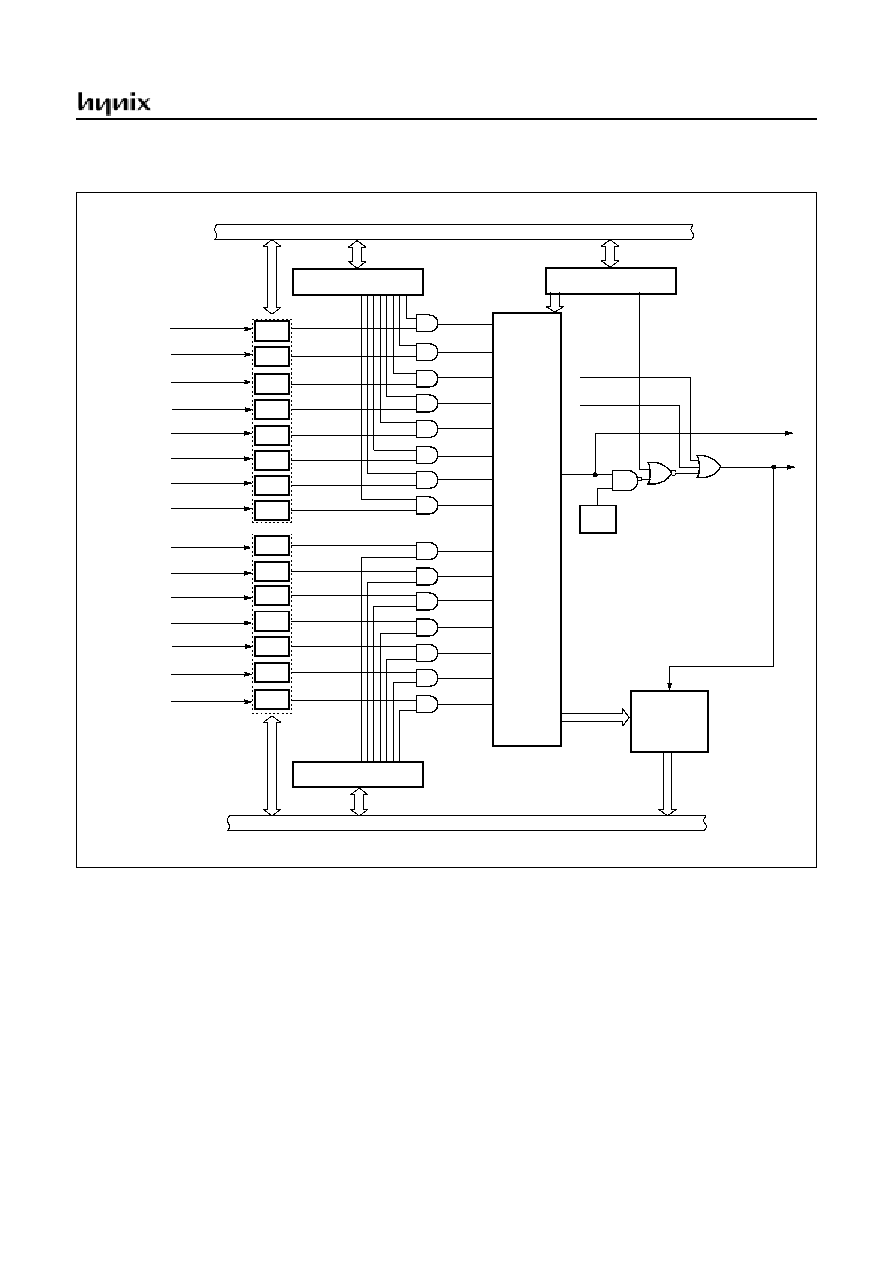
HMS81C4x60
November 2001 Ver 1.1
39
Figure 11-2 Block Diagram of Interrupt
T0
Timer 0
INT2
INT1
INT2
INT1
IFOSD
OSD
-
IENH [00F6
H
]
Interrupt Enable
IRQH
Interrupt
Vector
Address
Generator
Internal bus line
Register (Higher byte)
To CPU
Interrupt Master
Enable Flag
I Flag
Pri
o
rity
Co
n
t
ro
l
I-flag is in P SW , it is cleared by "D I", set by
"EI" instruction. W hen it goes interrupt service,
I-flag is cleared by hardw are, thus any other
interrupt are inhibited. W hen interrupt service is
com pleted by "R ET I" instruction, I-flag is set to
"1" by hardw are.
T2
Timer 2
SLICE
Slicer
VSync
IFVSync
WDT
IFWDT
IFBIT
BIT
-
IFI2C
I2C
IENL [00F4
H
]
IRQL
INTV
Intr. interval
T3
Timer 3
T1
Timer 1
[00F5
H
]
Internal bus line
IMOD [00F3
H
]
Bit5
Interrupt Enable
Register (Lower byte)
RESET
BRK
[0F7
H
]
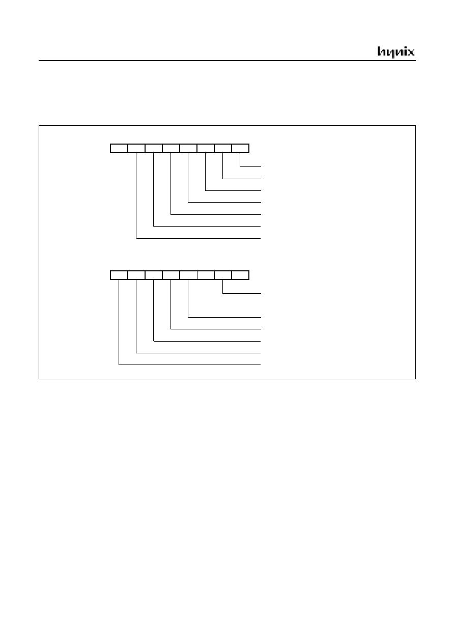
HMS81C4x60
40
November 2001 Ver 1.1
Interrupt request flag registers are shown in Figure 11-3.
Interrupt request is generated when suitable bit is set, and
suitable request flag of accepted interrup is clear when in-
terrupt processing cycle. Suitable bit is set when interrupt
request is occured, but no accepted request flag is set to
hold when the interrupt is accepted. Also, interrupt request
flag register(IRQH, IRQL) is the register of read or write.
So, request flag can be changed by program.
Figure 11-3 Interrupt Request Flag Registers
INT2
R/W
-
VSync interrupt request flag
INITIAL VALUE: 0000 0000
b
ADDRESS: 00F7
H
IRQH
OSD
MSB
LSB
SLICE VSync
T0
T2
INT1
R/W
R/W
WDT
R/W
T1
INITIAL VALUE: 0000 000-
b
ADDRESS: 00F5
H
IRQL
T3
MSB
I2C
BIT
INTV
R/W
R/W
R/W
-
R/W
R/W
R/W
R/W
R/W
R/W
R/W
R/W
Slicer interrupt request flag
Timer / Counter 2 interrupt request flag
Timer / Counter 0 interrupt request flag
External interrupt 2 interrupt request flag
External interrupt 1 interrupt request flag
On screen display interrupt request flag
I
2
C interrupt request flag
LSB
Basic interval timer interrupt request flag
Watch-dog timer interrupt request flag
Interrupt interval measurement interrupt request flag (INT3/4)
Timer / Counter 3 interrupt request flag
Timer / Counter 1 interrupt request flag
-
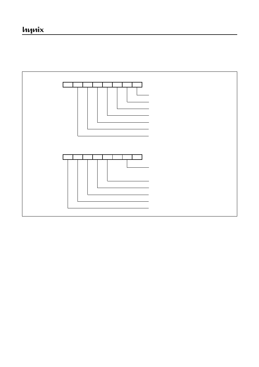
HMS81C4x60
November 2001 Ver 1.1
41
Interrupt enable flag registers are shown in Figure 11-4.
These registers are composed of interrupt enable flags of
each interrupt source, these flags determines whether an
interrupt will be accepted or not. When enable flag is "0",
a corresponding interrupt source is prohibited. Note that
PSW contains also a master enable bit, I-flag, which dis-
ables all interrupts at once.
Figure 11-4 Interrupt Enable Flag Regesters
INT2
R/W
-
VSync interrupt enable flag
INITIAL VALUE: 0000 0000
b
ADDRESS: 00F6
H
IENH
OSD
MSB
LSB
SLICE VSync
T0
T2
INT1
R/W
R/W
WDT
R/W
T1
INITIAL VALUE: 0000 000-
b
ADDRESS: 00F4
H
IENL
T3
MSB
I2C
BIT
INTV
R/W
R/W
R/W
-
R/W
R/W
R/W
R/W
R/W
R/W
R/W
R/W
Slicer interrupt enable flag
Timer / Counter 2 interrupt enable flag
Timer / Counter 0 interrupt enable flag
External interrupt 2 interrupt enable flag
External interrupt 1 interrupt enable flag
On screen display interrupt enable flag
I
2
C interrupt enable flag
LSB
Basic interval timer interrupt enable flag
Watch-dog timer interrupt enable flag
Interrupt interval measurement interrupt enable flag (INT3/4)
Timer / Counter 3 interrupt enable flag
Timer / Counter 1 interrupt enable flag
-
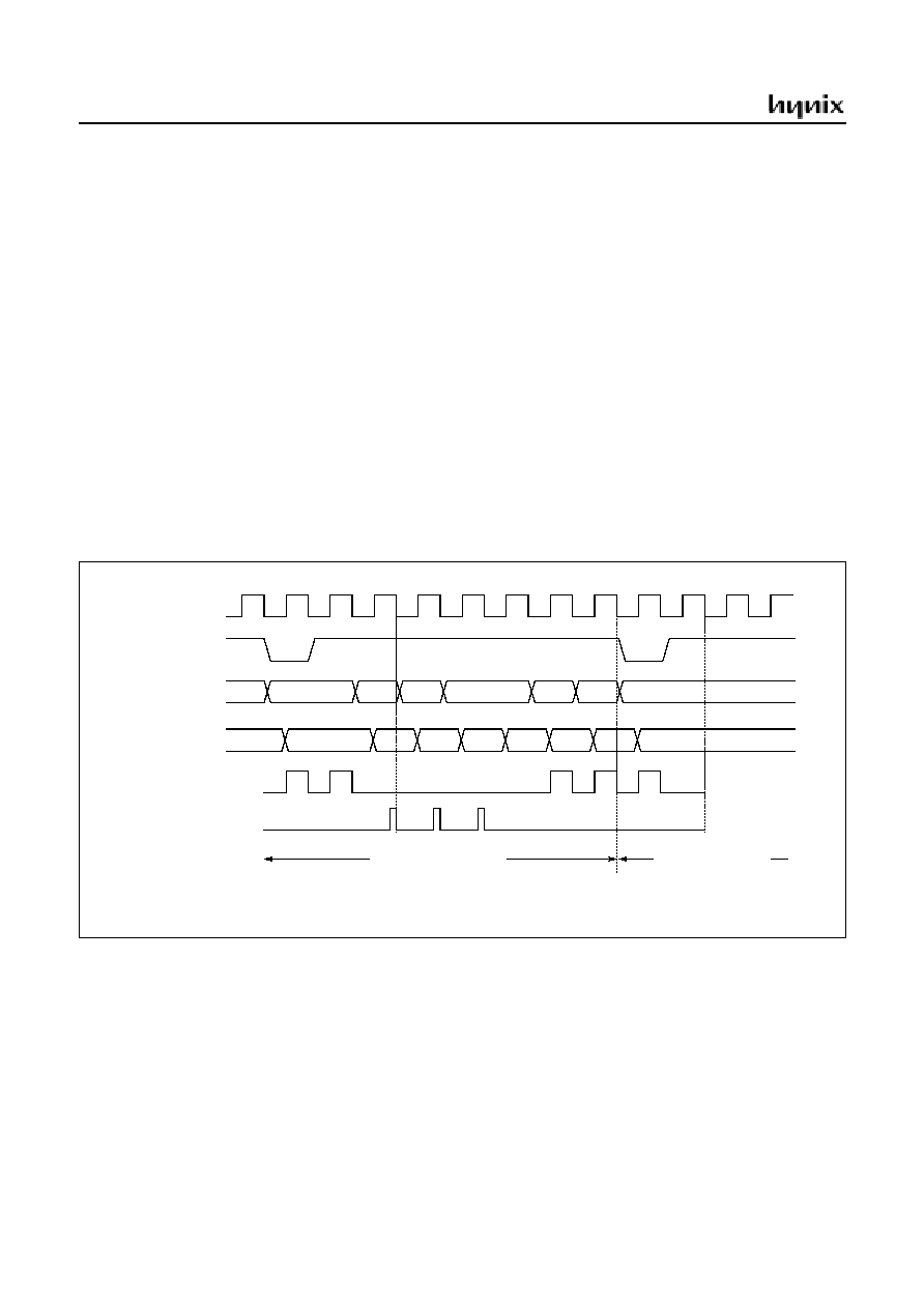
HMS81C4x60
42
November 2001 Ver 1.1
11.1 Interrupt Sequence
An interrupt request is held until the interrupt is accepted
or the interrupt latch is cleared to "0" by a reset or an in-
struction. Interrupt acceptance sequence requires 8 f
ex
(2
µ
s at f
MAIN
=4MHz) after the completion of the current in-
struction execution. The interrupt service task terminates
upon execution of an interrupt return instruction [RETI].
Interrupt acceptance
Figure 11-5 Interrupt Service routine Entering Timing
1. The interrupt master enable flag (I-flag) is cleared to
"0" to temporarily disable the acceptance of any fol-
lowing maskable interrupts. When a non-maskable in-
terrupt is accepted, the acceptance of any following
interrupts is temporarily disabled.
2. Interrupt request flag for the interrupt source accepted
is cleared to "0".
3. The contents of the program counter (return address)
and the program status word are saved (pushed) onto
the stack area. The stack pointer decrements 3 times.
4. The entry address of the interrupt service program is
read from the vector table address, and the entry ad-
dress is loaded to the program counter.
5. The instruction stored at the entry address of the inter-
rupt service program is executed.
V.L.
System clock
Address Bus
PC
SP
SP-1
SP-2
V.H.
New PC
V.L.
Data Bus
Not used
PCH
PCL
PSW
ADL
OP code
ADH
Instruction Fetch
Internal Read
Internal Write
Interrupt Processing Step
Interrupt Service Task
V.L. and V.H. are vector addresses.
ADL and ADH are start addresses of interrupt service routine as vector contents.
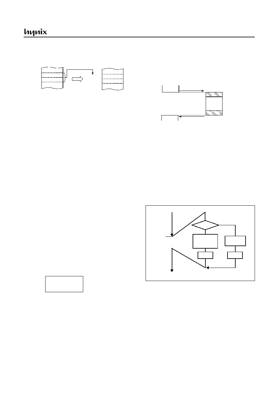
HMS81C4x60
November 2001 Ver 1.1
43
A maskable interrupt is not accepted until the I-flag is set
to "1" even if a maskable interrupt of higher priority than
that of the current interrupt being serviced.
When nested interrupt service is necessary, the I-flag is set
to "1" in the interrupt service program. In this case, accept-
able interrupt sources are selectively enabled by the indi-
vidual interrupt enable flags.
Saving/Restoring General-purpose Register
During interrupt acceptance processing, the program
counter and the program status word are automatically
saved on the stack, but not the accumulator and other reg-
isters. These registers are saved by the program if neces-
sary. Also, when nesting multiple interrupt services, it is
necessary to avoid using the same data memory area for
saving registers.
The following method is used to save/restore the general-
purpose registers.
Example: Register save using push and pop instructions
General-purpose register save/restore using push and pop
instructions;
11.2 BRK Interrupt
Software interrupt can be invoked by BRK instruction,
which is the lowest priority order.
Interrupt vector address of BRK is shared with the vector
of TCALL 0 (Refer to Program Memory Section). When
BRK interrupt is generated, B-flag of PSW is set to distin-
guish BRK from TCALL 0.
Each processing step is determined by B-flag as shown in
Figure 11-6.
Figure 11-6 Execution of BRK/TCALL0
INTxx:
PUSH
A
PUSH
X
LDA
DPGR
PUSH
A
;SAVE ACC.
;SAVE X REG.
;SAVE DPGR
; Direct page
; accessable reg.
;
:
interrupt processing
:
POP
A
STA
DPGR
POP
X
POP
A
RETI
;RESTORE DPGR
;RESTORE X REG.
;RESTORE ACC.
;RETURN
Basic Interval Timer
012
H
0E3
H
0FFE6
H
0FFE7
H
0E
H
2E
H
0E312
H
0E313
H
Entry Address
Correspondence between vector table address for BIT interrupt
and the entry address of the interrupt service program.
Vector Table Address
main task
interrupt
service task
saving
registers
restoring
registers
acceptance of
interrupt
interrupt return
B-FLAG
BRK
INTERRUPT
ROUTINE
RETI
TCALL0
ROUTINE
RET
BRK or
TCALL0
=0
=1

HMS81C4x60
44
November 2001 Ver 1.1
11.3 Multi Interrupt
If two requests of different priority levels are received si-
multaneously, the request of higher priority level is ser-
viced. If requests of the same priority level are received
simultaneously, an internal polling sequence determines
by hardware which request is serviced.
Figure 11-7 Execution of Multi Interrupt
However, multiple processing through software for special
features is possible. Generally when an interrupt is accept-
ed, the I-flag is cleared to disable any further interrupt. But
as user set I-flag in interrupt routine, some further interrupt
can be serviced even if certain interrupt is in progress.
Example: Even though Timer1 interrupt is in progress,
INT0 interrupt serviced without any suspend.
TIMER1:
PUSH
A
PUSH
X
PUSH
Y
LDM
IENH,#20H
;
Enable INT1 only
LDM
IENL,#0
;
Disable other
EI
;
Enable Interrupt
:
:
:
:
:
:
LDM
IENH,#FFH
;
Enable all interrupts
LDM
IENL,#FEH
POP
Y
POP
X
POP
A
RETI
enable INT0
TIMER 1
service
INT0
service
Main Program
service
Occur
TIMER1 interrupt
Occur
INT0
EI
disable other
enable INT0
enable other
In this example, the INT0 interrupt can be serviced without any
pending, even TIMER1 is in progress.
Because of re-setting the interrupt enable registers IENH,IENL
and master enable "EI" in the TIMER1 routine.

HMS81C4x60
November 2001 Ver 1.1
45
11.4 External Interrupt
The external interrupt on INT1, INT2... pins are edge trig-
gered depending the edge selection register.
Refer to "6. PORT STRUCTURES" on page 12.
The edge detection of external interrupt has three transition
activated mode: rising edge, falling edge, both edge.
Figure 11-8 External Interrupt Block Diagram
INT1, INT2 and INT3 are multiplexed with general I/O
ports. To use external interrupt pin, the bit of port function
register FUNC1 should be set to "1" correspondingly.
Response Time
The INT1, INT2 and INT3 edge are latched into INT1IF,
INT2IF and INT3IF at every machine cycle. The values
are not actually polled by the circuitry until the next ma-
chine cycle. If a request is active and conditions are right
for it to be acknowledged, a hardware subroutine call to the
requested service routine will be the next instruction to be
executed. For example, the DIV instruction takes twelve
machine cycles. Thus, a minimum of twelve complete ma-
chine cycles elapse between activation of an external inter-
rupt request and the beginning of execution of the first
instruction of the service routine
Figure 11-9 Interrupt Response Timing Diagram ( Interrupt overhead )
INT1IF
INT1 pin
INT1 INTERRUPT
INT2IF
INT2 pin
INT2 INTERRUPT
INT3IF
INT3 pin
INT3 INTERRUPT
IEDS
[00F2
H
]
e
dge
se
l
e
ction
System clock
Instruction Fetch
Last instruction execution (0~12cycle)
Enter interrupt service routine (8cycle)
Interrupt request sampling
1cycle
Interrupt overhaed (9~21cycle)
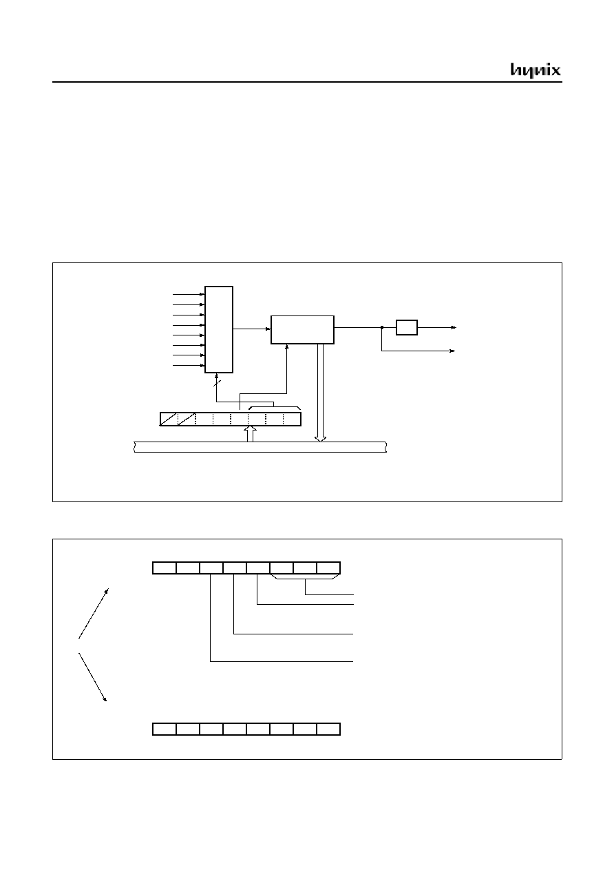
HMS81C4x60
46
November 2001 Ver 1.1
12. TIMER
12.1 Basic Interval Timer
The HMS81C4x60 has one 8-bit Basic Interval Timer that
is free-run and can not be stopped. Block diagram is shown
in Figure 12-1.
The Basic Interval Timer generates the time base for
watchdog timer counting, and etc. It also provides a Basic
interval timer interrupt (BITIF). As the count overflow
from FF
H
to 00
H
, this overflow causes the interrupt to be
generated. The Basic Interval Timer is controlled by the
clock control register (CKCTLR) shown in Figure 12-2.
Source clock can be selected by lower 3 bits of CKCTLR.
BITR and CKCTLR are located at same address, and ad-
dress 00D6
H
is read as a BITR and written to CKCTLR..
Figure 12-1 Block Diagram of Basic Interval Timer
Figure 12-2 BITR Basic Interval Timer Mode Register
MUX
Basic Interval Timer Interrupt
BITR
Select Input clock
3
source
clock
8-bit up-counter
BITCK
BTCL
f
ex
˜
2
10
f
ex
˜
2
9
f
ex
˜
2
8
f
ex
˜
2
7
f
ex
˜
2
6
f
ex
˜
2
5
f
ex
˜
2
4
Watchdog timer clock (WDTCK)
clear
overflow
Internal bus line
[0D6
H
]
[0D6
H
]
BITIF
Clock control register
CKCTLR
WDT ENPCK BTCL BTS2 BTS1 BTS0
ON
PS4
PS5
PS6
PS7
PS8
PS9
PS10
PS11
f
ex
˜
2
11
INITIAL VALUE: Undefined
ADDRESS: 00D6
H
MSB
LSB
R
R
R
R
R
R
R
R
BITR
INITIAL VALUE: --00 0000
b
ADDRESS: 00D6
H
MSB
LSB
B.I.T Clock
B.I.T clear (when write)
B.I.T value (when read)
W
W
W
W
W
W
W
W
B T S 1
B TS 2
B TC L
E N P C K
W D TO N
-
-
B T S 0
CKCTLR
0 : B.I.T Free-run
1 : B.I.T clear (Auto reset when after 1 cycle)
Peripherial clock enable (write time)
0 : Peripherial clock stop
1 : Peripherial clock supply
WDT function control
0 : 6 bit TIMER
1 : WATCH-DOG TIMER
Caution:
Both register are in same address,
when write, to be a CKCTLR,
when read, to be a BITR.
8-BIT BINARY COUNTER

HMS81C4x60
November 2001 Ver 1.1
47
12.2 Timer 0, 1
Timer 0, 1 consists of prescaler, multiplexer, 8-bit compare
data register, 8-bit count register, Control register, and
Comparator as shown in Figure 12-3 and Figure 12-4.
These Timers can run separated 8bit timer or combined
16bit timer. These timers are operated by internal clock.
The contents of TDR1 are compared with the contents of
up-counter T1. If a match is found, a timer/counter 1 inter-
rupt (T1IF) is generated, and the counter is cleared. Count-
ing up is resumed after the counter is cleared.
Note: You can read Timer 0, Timer 1 value from TDR0 or
TDR1. But if you write data to TDR0 or TDR1, it changes
Timer 0 or Timer 1 modulo data, not Timer value.
The content of TDR0, TDR1 must be initialized (by soft-
ware) with the value between 01
H
and FF
H
,not to 00
H
.
Or not, Timer 0 or Timer 1 can not count up forever.
The control registers for Timer 0,1 are shown below.
Figure 12-3 Timer / Event Count 0,1
(Example) TIMER0 1mS TIME INTERVAL INTERRUPT
:
:
TDR_CNT:
LDM
TDR0,#249
LDM
TDR1,#0
LDM
TM0,#0011_1101b
; 4uSEC PRESCALER FOR T0
:
:
INITIAL VALUE: -000 0000
b
ADDRESS: 00D0
H
MSB
LSB
T0 input clock select(f
ex
=4MHz)
Timer 0 Continue/Hold control
R/W
R/W
R/W
R/W
R/W
R/W
R/W
R/W
T 0S L1
T 0C N
T 0S T
T1S L0
T1S L1
T 1S T
-
T 0S L0
TM0
00 : PS2(1
µ
S)
0 : Count Hold
1 : Count Countinue
01 : PS4(4
µ
S)
10 : PS6(16
µ
S)
11 : PS8(64
µ
S)
Timer 0 Start control
0 : Count Hold
1 : Count Clear and Start
Timer 1 input clock(f
ex
=4MHz)
00 : Timer 0 overflow (16bit mode)
01 : PS2(1
µ
S)
10 : PS4(4
µ
S)
11 : PS6(16
µ
S)
Timer 1Start/Hold control
0 : Count Hold
0 : Count Clear and Start
MSB
LSB
R/W
R/W
R/W
R/W
R/W
R/W
R/W
R/W
TDR0
INITIAL VALUE: Undefined
ADDRESS: 00D2
H
MSB
LSB
R/W
R/W
R/W
R/W
R/W
R/W
R/W
R/W
TDR1
INITIAL VALUE: Undefined
ADDRESS: 00D3
H

HMS81C4x60
48
November 2001 Ver 1.1
.
Figure 12-4 Simplified Block Diagram of 8bit Timer0, 1
Figure 12-5 Count Example of Timer
8bit Comparator
Internal bus line
TM0
TDR0
Timer 0
T0IF
Clock
TDR1
Timer 1
Clock
Clear
Clear
8bit Comparator
T1IF
MUX
PS2
PS4
PS6
PS8
MUX
NC
PS2
PS4
PS6
T0CN
T0ST
T1ST
Timer 0 (T0IF)
Interrupt
TDR0
TIME
Occur interrupt
Occur interrupt
stop
clear & start
disable
enable
Start & Stop
T0ST
T0CN
Control count
up-c
ount
~~
~~
T0ST = 0
T0ST = 1
T0CN = 0
T0CN = 1
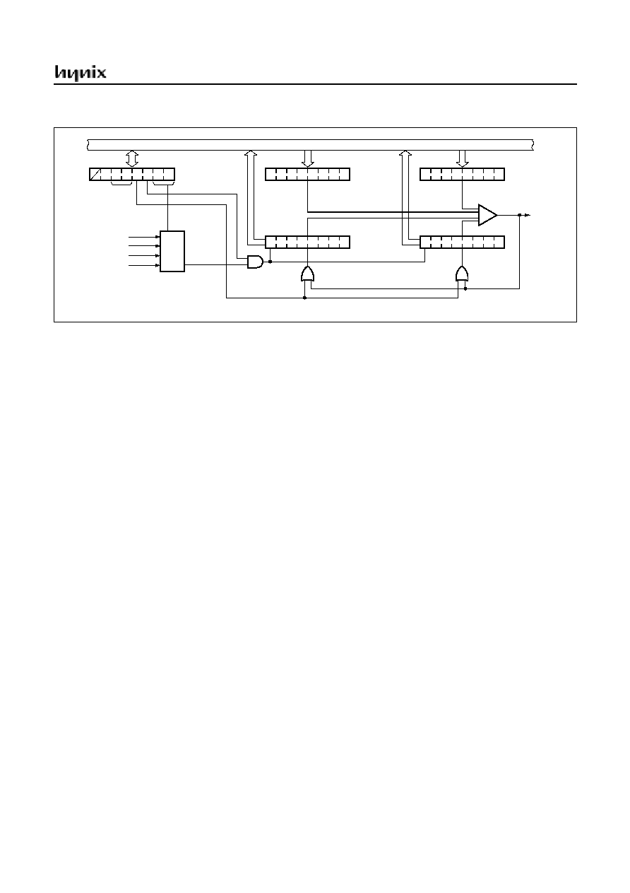
HMS81C4x60
November 2001 Ver 1.1
49
Figure 12-6 Simplified Block Diagram of 16bit Timer0, 1
Internal bus line
TM0
TDR0
Timer 0
Clock
TDR1
Timer 1
Clock
Clear
Clear
16bit Comparator
T1IF
MUX
PS2
PS4
PS6
PS8
T0CN
T0ST
0
0
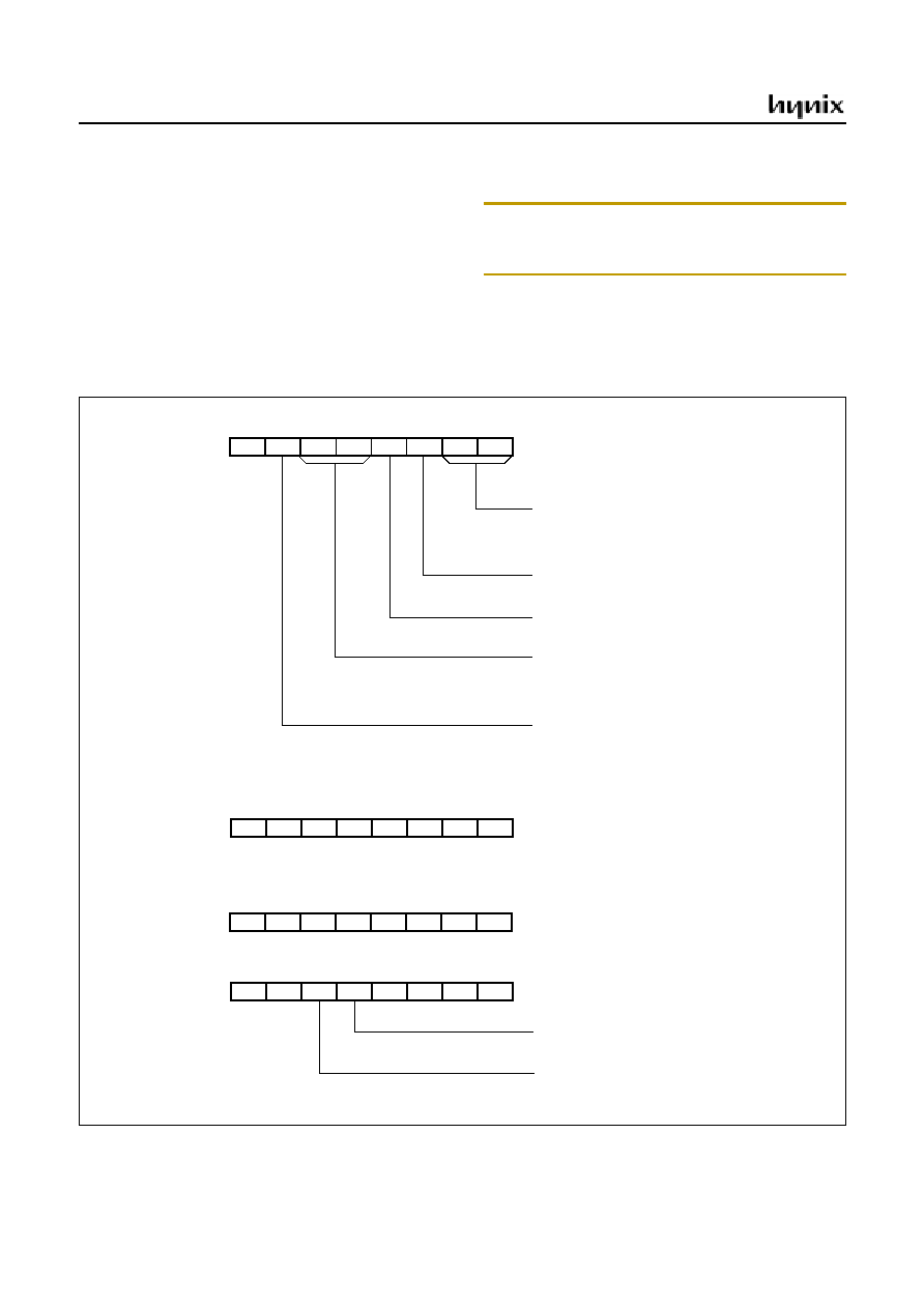
HMS81C4x60
50
November 2001 Ver 1.1
12.3 Timer / Event Counter 2, 3
Timer 2, 3 consists of prescaler, multiplexer, 8-bit compare
data register, 8-bit count register, Control register, and
Comparator as shown in Figure 12-7 and Figure 12-8.
These Timers have two operating modes. One is the timer
mode which is operated by internal clock, other is event
counter mode which is operated by external clock from pin
R24/EC2, R25/EC3.
These Timers can run separated 8bit timer or combined
16bit timer.
Note: You can read Timer 2, Timer 3 value from TDR2 or
TDR3. But if you write data to TDR2 or TDR3, it changes
Timer 2 or Timer 3 modulo data, not Timer value.
The content of TDR2, TDR3 must be initialized (by soft-
ware) with the value between 01
H
and FF
H
,not to 00
H
.
Or not, Timer 2 or Timer 3 can not count up forever.
The control registers for Timer 2,3 are shown below
Figure 12-7 Timer / Event Count 2,3
INITIAL VALUE: -000 0000
b
ADDRESS: 00D1
H
MSB
LSB
T2 input clock select
Timer 2 Continue/Hold control
R/W
R/W
R/W
R/W
R/W
R/W
R/W
R/W
T3S L1
T3C N
T3S T
T 3S L0
T 3S L1
T3S T
-
T3S L0
TM2
00 : External EVENT input(EC2)
0 : Count Hold
1 : Count Countinue
01 : PS2(1
µ
S)
10 : PS4(4
µ
S)
11 : PS6(16
µ
S)
Timer 2 Start/Hold control
0 : Count Hold
1 : Count Clear and Start
Timer 3 input clock
00 : Connected to T2(16bit mode)
01 : External EVENT input(EC3)
10 : PS2 (1
µ
S)
11 : PS6 (16
µ
S)
Timer 3 Start/Hold control
0 : Count Hold
0 : Count Clear and Start
MSB
LSB
R/W
R/W
R/W
R/W
R/W
R/W
R/W
R/W
T D R 1
TD R 2
TD R 3
TD R 4
TD R 5
T D R 6
T D R 7
TD R 0
TDR2
INITIAL VALUE: Undefined
ADDRESS: 00D4
H
MSB
LSB
R/W
R/W
R/W
R/W
R/W
R/W
R/W
R/W
TD R 1
TD R 2
TD R 3
TD R 4
TD R 5
TD R 6
TD R 7
TD R 0
TDR3
INITIAL VALUE: Undefined
ADDRESS: 00D5
H
INITIAL VALUE: 0000 000-
b
ADDRESS: 00CE
H
MSB
LSB
W
W
W
W
W
W
W
W
IN T1S
IN T 2S
IN T 3S
E C 0S
E C 1S
-
-
-
FUNC
R24/EC2 Select
R25/EC3 Select
0 : R24
1 : EC2
0 : R25
1 : EC3
HMS81C4x60
November 2001 Ver 1.1
51
.
Figure 12-8 Simplified Block Diagram of 8bit Timer/Event Counter 2,3
Figure 12-9 Count Example of Timer / Event counter
8bit Comparator
Internal bus line
TM2
TDR2
Timer 2
T2IF
Clock
TDR3
Timer 3
Clock
Clear
Clear
8bit Comparator
T3IF
MUX
EC2
PS2
PS4
PS6
MUX
NC
EC3
PS2
PS4
T2CN
T2ST
T3ST
Timer 2 (T2IF)
Interrupt
TDR2
TIME
Occur interrupt
Occur interrupt
stop
clear & start
disable
enable
Start & Stop
T2ST
T2CN
Control count
up-
co
unt
~~
~~
T2ST = 0
T2ST = 1
T2CN = 0
T2CN = 1
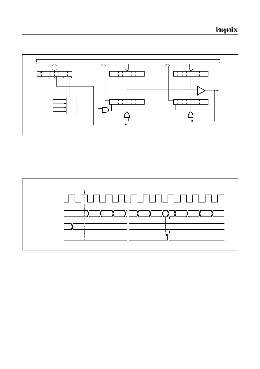
HMS81C4x60
52
November 2001 Ver 1.1
Figure 12-10 Simplified Block Diagram of 16bit Timer/Event Counter 2,3
Timer Mode
In the timer mode, the internal clock is used for counting
up. Thus, you can think of it as counting internal clock in-
put. The contents of TDRn (n=0~3) are compared with the
contents of up-counter, Timer n. If match is found, a timer
n interrupt (TnIF) is generated and the up-counter is
cleared to 0. Counting up is resumed after the up-counter
is cleared.
As the value of TDRn is changeable by software, time in-
terval is set as you want
U
Figure 12-11 Timer Mode Timing Chart
Event Counter Mode
In event timer mode, counting up is started by an external
trigger. This trigger means falling edge of the ECn (n=0~1
) pin input. Source clock is used as an internal clock select-
ed with TM2. The contents of TDRn are compared with the
contents of the up-counter. If a match is found, an TnIF in-
terrupt is generated, and the counter is cleared to 00
H
. The
counter is restarted by the falling edge of the ECn pin in-
put.
The maximum frequency applied to the ECn pin is f
ex
/2
[Hz] in main clock mode.
In order to use event counter function, the bit EC0S, EC1S
of the Port Function Select Register FUNC(address 0CE
H
)
is required to be set to "1".
After reset, the value of TDRn is undefined, it should be
Internal bus line
TM2
TDR2
Timer 2
Clock
TDR3
Timer 3
Clock
Clear
Clear
16bit Comparator
T3IF
MUX
EC2
PS4
PS6
PS8
T0CN
T0ST
0
0
0
N-2
2
0
N
3
N-1
N
~~
~~
~~
Source clock
Up-counter
TDRn (n=0~3)
TnIF (n=0~3) interrupt
Start count
~~
1
2
3
~~
~~
1
4
Match
Detect
Counter
Clear

HMS81C4x60
November 2001 Ver 1.1
53
initialized to between 01
H
~FF
H
S not to 00
H
U
Figure 12-12 Event Counter Mode Timing Chart
The interval period of Timer is calculated as below equa-
tion.
Figure 12-13 Count Example of Timer / Event counter
0
1
2
1
0
N
2
~~
~~
~~
N-1
N
~~
~~
~~
ECn (n=2~3) pin
Up-counter
TDRn (n=2~3)
TnIF (n=2~3) interrupt
Start count
Period
1
f
e x
------
Prescaler
◊
ratio
TDR
◊
n
=
~~
Timer 2 (T2IF)
Interrupt
TDR2
TIME
Occur interrupt
Occur interrupt
Occur interrupt
Interrupt period
up
-c
oun
t
~~
~~
0
1
2
3
4
5
6
7
8
n
n-1
P
CP
= P
CP
x n
n-2
TDR2=n
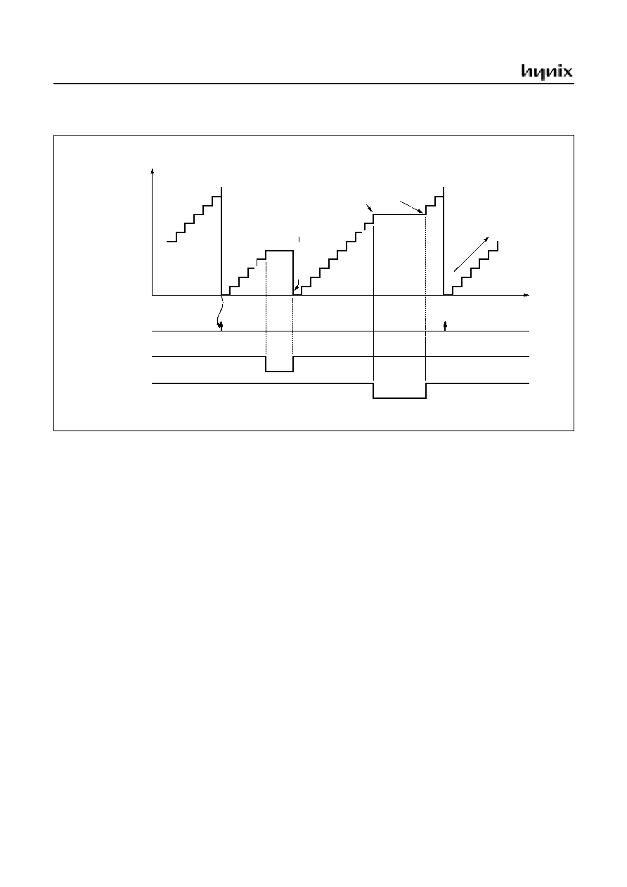
HMS81C4x60
54
November 2001 Ver 1.1
Figure 12-14 Count Operation of Timer / Event counter
Timer 2 (T2IF)
Interrupt
TDR2
TIME
Occur interrupt
Occur interrupt
stop
clear & start
disable
enable
Start & Stop
T2ST
T2CN
Control count
up-
co
unt
~~
~~
T2ST = 0
T2ST = 1
T2CN = 0
T2CN = 1
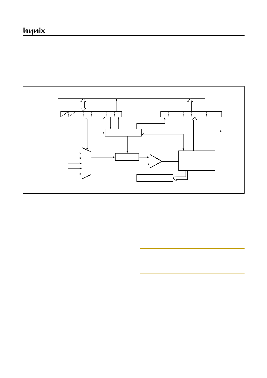
HMS81C4x60
November 2001 Ver 1.1
55
13. A/D Converter
The A/D converter circuit is shown in Figure 13-1.
The A/D converter circuit consists of the comparator and
c o n t r o l r e g i s t e r A I P S ( 0 0 E F
H
) , A D C M ( 0 0 F 0
H
) ,
ADR(00F1
H
). The AIPS register select normal port or an-
alog input. The ADCM register control A/D converter's
activity. The ADR register stores A/D converted 8bit re-
sult. The more details are shown Figure 13-2.
Figure 13-1 Block Diagram of A/D convertor circuit
Control
The HMS81C4x60 contains a A/D converter module
which has six analog inputs.
1. First of all, you have to select analog input pin by set the
ADCM and AIPS.
2. Set ADEN (A/D enable bit : ADCM bit5).
3. Set ADST (A/D start bit : ADCM bit1). We recommend
you do not set ADEN and ADST at once, it makes worse
A/D converted result.
4. ADST bit will be cleared 1 cycle automatically after you
set this.
[Example]
;Set AIPS, change ? to what you want
;
0 : digital port
;
1 : analog port
LDM AIPS,#0000_1000b
; Set ADEN, xxx is analog port number
LDM ADCM,#0010_1100b
; or "SET1 ADEN"
; Set ADST, xxx is analog port number
LDM ADCM,#0010_11110b
BBC
ADCM.ADSF,$
LDA
ADR
; or "SET1 ADST"
:
:
5. After A/D conversion is completed, ADSF bit and inter-
rupt flag IFA will be set. (A/D conversion takes 36 ma-
chine cycle : 18uS when f
ex
=4MHz).
Note: Make sure AIPS bits, if you using a port which is set
digital input by AIPS, analog voltage will be flow into MCU
internal logic not A/D converter. Sometimes device or port
is damaged permanently.
Comparator
AN0
MUX
AN1
AN2
AN3
port
select
+
-
S/H
ADCM [F0
H
]
ADEN ADS2 ADS1 ADS0 ADST ADSF
ADR [F1
H
]
AN4
Control circuit
Register ladder
Succesive
Approximation
Circuit
IFA
Vref
5
0
Data Bus
0 1 2 3 4 5 6 7
8
8
8
HMS81C4x60
56
November 2001 Ver 1.1
Figure 13-2 A/D convertor Registers
Figure 13-3 A/D Conversion Data Register
INITIAL VALUE: --01 1101
b
ADDRESS: 00F0
H
MSB
LSB
A/D Converter Status bit
A/D Converter Start bit
R/W
R/W
R/W
R/W
R/W
R/W
R/W
R
A D S T
A D S 0
A D S 1
A D S 2
A D E N
-
-
A D S F
ADCM
0 : Busy
0 : Ignore
1 : A/D start (`0' after 1 cycle)
1 : A/D conversion completed
Analog Port Select
000 : AN0 select
001 : AN1 select
010 : AN2 select
011 : AN3 select
A/D Converter Enable bit
0 : Disable
1 : Enable
100 : AN4 select
101 : Default
110 : Default
111 : Default
MSB
LSB
R
R
R
R
R
R
R
R
TD R 1
T D R 2
T D R 3
T D R 4
T D R 5
T D R 6
T D R 7
TD R 0
ADR
INITIAL VALUE: Undefined
ADDRESS: 00F1
H
MSB
LSB
W
W
W
W
W
W
W
W
A IP S 1
A IP S 2
A IP S 3
A IP S 4
-
-
-
A IP S 0
AIPS
INITIAL VALUE: ---0 0000
H
ADDRESS: 00EF
H
Analog Input Select
0 : P1 input
1 : ADC Input
ADS2
ADS1
ADS0
Function
PORT select
R14/AN4
R13/AN3
R12/AN2
R11/AN1
R10/AN0
9
0
9
AN0
R14
R13
R12
R11
AN0
9
0
:
AN1
R14
R13
R12
AN1
R10
0
1
9
AN2
R14
R13
AN2
R11
R10
0
1
:
AN3
R14
AN3
R12
R11
R10
1
0
9
AN4
AN4
R13
R12
R11
R10
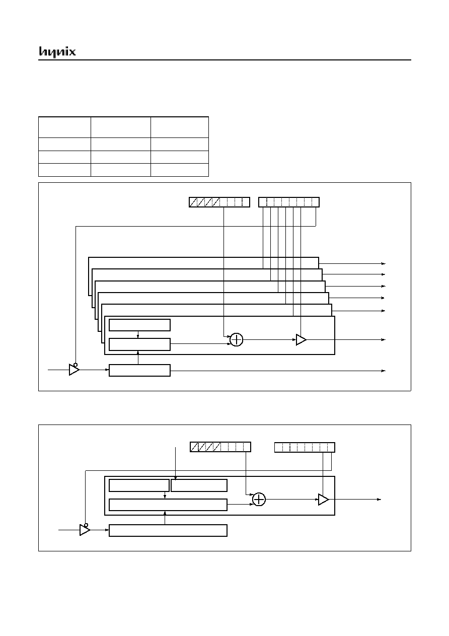
HMS81C4x60
November 2001 Ver 1.1
57
14. Pulse Width Modulation (PWM)
The PWM circuit is shown in Figure 14-1, .
The PWM circuit consists of the counter, comparator, Data
register.
The PWM control registers are PWMR4~0, PWMCR2~1,
PWM5H, PWM5L.
The more details about registers are shown Figure 14-2 .
Figure 14-1 8bit register (PWM7~0) circuit
Figure 14-2 14bit register (PWM8) circuit
Example
(f
ex
=4MHz)
14bit PWM
8bit PWM
Resolution
14 bits
8 bits
Input Clock
2MHz
250KHz
Frame cycle
8,192uS
1,024uS
PWMCR2 [EB
H
]
8bit counter
PWM0
PWMCR1 [EA
H
]
8bit comparator
PWMR0 [E0
H
]
EN
5
EN
4
EN
3
EN
2
EN
1
EN
0
PWMR1 [E1
H
]
PWMR2 [E2
H
]
PWMR3 [E3
H
]
PWMR4 [E4
H
]
PWMR5 [E5
H
]
PWM5
PWM4
PWM3
PWM2
PWM1
IF1Frame
PS5
CNTB
CNTB
EN5
EN4
EN3
EN2
EN1
EN0
3 2 1 0
PWMCR2 [EB
H
]
14bit counter
PWM8
PWMCR1 [EA
H
]
14bit comparator
PWMR5H 8bit [E8
H
]
EN8
PS2
CNTB
PWMR5L 6bit [E9
H
]
MSB
LSB
In
t
e
r
n
al
C
o
nt
r
o
l
CNT
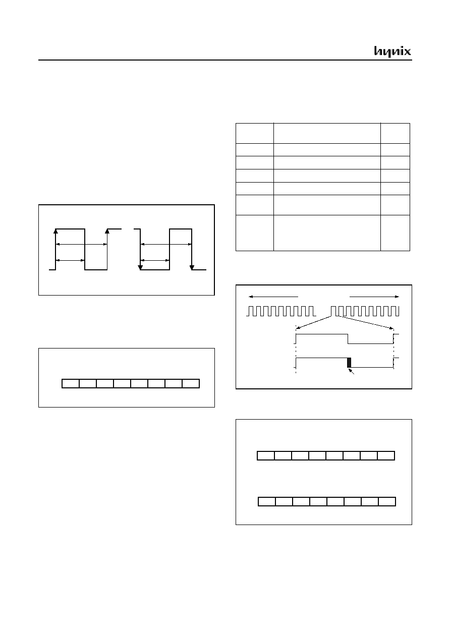
HMS81C4x60
58
November 2001 Ver 1.1
8bit PWM Control
The HMS81C4x60 contains a one 14bit PWM and five
8bit PWM module.
1. 8bit PWM0~5 is wholy same internal circuit, but
PWM0~5 output port is CMOS bidirectional I/O pin.
2. Al l PWM polarity has the same by POL2's value.
3. Calulate Frame cycle and Pulse width is as following.
PWM Frame Cycle = 2
13
/ f
ex
(Sec)
PWM Width = (PWMRn+1)
◊
2
5
/ f
ex
(n=0~5)
Pulse Duty (%) = (PWMRn +1) / 256
◊
100(%) (n=0~5)
Figure 14-3 Wave form example for 8bit PWM
4. PWM output is enabled during ENn(n=0~5) bit (See
PWMCR1~2) contains 1.
Figure 14-4 8bit PWM Registers
5. CNTB controls all PWM counter enable.
If CNTB=0, than Counter is disabled.
14bit PWM Control
1. 14bit PWM's operation concept is not the same as 8bit
PWM.
1 PWM frame contains 64 sub PWMs.
PWM5H : Set sub PWM's basic Pulse Width.
PWM5L : Number of sub PWM which is added 1 clock.
2. PWM polarity is selected by POL1's value.
If POL1=0, Positive Polarity.
3. Calulate Frame cycle and Pulse width is as following.
Main PWM Frame Cycle = 2
16
/ f
ex
(Sec).
Sub PWM Frame Cycle = Main Frame Cycle / 64.
4. Table 14-1, "PWM5L and Sub frame matching table,"
on page 58 show PWM5L function.
Figure 14-5 Wave form example for 14bit PWM
Figure 14-6 PWM5H, PWM5L Register
Positive Polarity (POL2=0)
1
2
Negative Polarity (POL2=1)
1
2
1. Frame cycle
2. Pulse Width
MSB
LSB
R/W
R/W
R/W
R/W
R/W
R/W
R/W
R/W
PW M0D7
PWMR4~0
INITIAL VALUE: Undefined
ADDRESS: 00E0
H
~E4
H
PW M0D6 PW M0D5 PW M0D4 PW M0D3 PW M0D2 PW M0D1 PW M0D0
Each PWM Data Store
Bit value
Sub frame number which is
added 1 clock
Pulse
count
if Bit0=1
32
1
if Bit1=1
16, 48
2
if Bit2=1
8, 24, 40, 56
4
if Bit3=1
4, 12, 20, 28, 36, 44, 52, 60
8
if Bit4=1
2, 6, 10, 14, 18, 22, 26, 30, 34,
38, 42, 46, 50, 54
16
if Bit5=1
1, 3, 5, 7, 9, 11, 13, 15, 17, 19,
21, 23, 25, 27, 29, 31, 33, 35, 37,
39, 41, 43, 45, 47, 49, 51, 53, 55,
57, 59, 61, 63
32
Table 14-1 PWM5L and Sub frame matching table
Main PWM Frame
.....
0
1 2
61 62 63
Sub PWM Frame
Sub PWM Frame
which is added
1 clock
1 clock width : PS2
MSB
LSB
R/W
R/W
R/W
R/W
R/W
R/W
R/W
R/W
PWM 5H7
PW M5H
INITIAL VALUE: Undefined
ADDRESS: 00E8
H
MSB
LSB
R/W
R/W
R/W
R/W
R/W
R/W
R/W
R/W
PWM5L
INITIAL VALUE: Undefined
ADDRESS: 00E9
H
PW M5H6 PW M5H5 PW M5H4 PW M5H3 PW M5H2 PW M5H1 PW M5H0
PW M5L0
PW M5L1
PW M5L3
PW M5L4
PW M5L5
-
-
PW M5L2
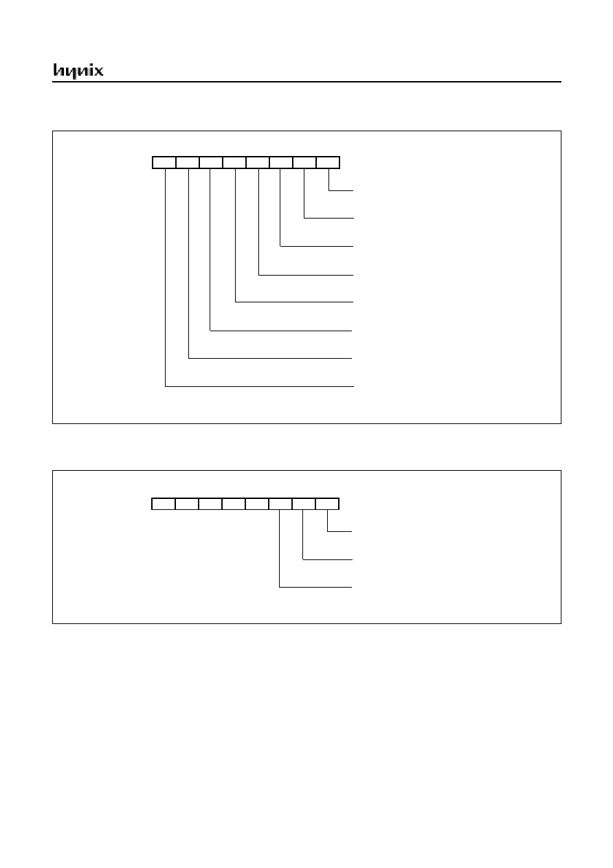
HMS81C4x60
November 2001 Ver 1.1
59
Figure 14-7 PWM Control Register 1
Figure 14-8 PWM Control Register 2
INITIAL VALUE: 0000 0000
b
ADDRESS: 00EA
H
MSB
LSB
R30/PWM0 Select
R31/PWM1 Select
R/W
R/W
R/W
R/W
R/W
R/W
R/W
R/W
E N 1
E N 2
E N 3
E N 4
E N 5
B U Z
TM R 1
E N 0
PW MCR1
0 : R30
0 : R31
1 : PWM1
1 : PWM0
R32/PWM2 Select
0 : R32
1 : PWM2
R33/PWM3 Select
0 : R33
1 : PWM3
R34/PWM4 Select
0 : R34
1 : PWM4
R35/PWM5 Select
0 : R35
1 : PWM5
R3
]
/
Buzzer
Select
0 : R36
1 : Buzzer output
R37/TMR1 Select
0 : R37
1 : TMR1
INITIAL VALUE: 0000 0000
b
ADDRESS: 00EB
H
MSB
LSB
14Bit/8Bit PWM Count stop/start
14Bit PWM Output Polarity
R/W
R/W
R/W
R/W
R/W
R/W
R/W
R/W
P O L14
P O L8
-
-
-
-
-
C N TB
PWMCR2
0 : Count start
0 : Positive Polarity
1 : Negitive Polarity
1 : Count stop
8Bit PWM Output Polarity
0 : Positive Polarity
1 : Negative Polarity

HMS81C4x60
60
November 2001 Ver 1.1
15. Interrupt Interval Measurement Circuit
The Interrupt interval measurement circuit is shown in Fig-
ure 15-1.
The Interrupt interval measurement circuit consists of the
input multiplexer, sampling clock multiplexer, Edge detec-
tor, 8bit counter, measured result storing register, FIFO (9
bit, 6 level) interrupt, Control register, etc.
The more details about registers are shown Figure 15-2 .
Figure 15-1 Block Diagram of Interrupt interval measurement circuit
Control
The HMS81C4x60 contains a Interrupt interval measure-
ment module.
1. Select interrupt input pin what you want to measure by
set the FUNC [00CE
H
].
2. Set IDCR [00F9
H
] : FIFO clear, interrupt mode select,
interrupt edge select, external interrupt INT3 select, sam-
pling clock select, COUNT start/stop select.
3. Set IDCR [00F9
H
] : set IDST to start measuring.
4. Counter value is stored to IDR [00FB
H
] when selected
edge is detected. After data was written, timer is cleard au-
tomatically and it counts continue.
5
. You can select interrupt occuring point by set Interrupt
Mode Select bit (IMS), every edge what you selected or
FIFO 4 level is filled.
6. If input signal's interval is larger than maximum counter
value (0FF
H
), counter occurring an interrupt and count
again from 00
H
.
7. See Figure 15-7 FIFO operating mechanism.
[Example]
;Set INT3 for remote control pulse
reception
LDM
FUNC,#0000_1001b;INT3 SET
LDM
IDCR,#1001_0001b ;64uSec PCS
:
:
MUX
IDCR [F9
H
]
I34H
I34L
ISEL
IDCK
IDST
IDFS [FA
H
]
INT3
8bit counter
FIFO
(9bit, 6level)
INT34
IMS
1
0
DPOL
FOE
FFUL FEMP
FCLR
MUX
PS8
PS9
1
0
MUX
0
1
Edge detector
Clear
IDR [FB
H
]
D7
D6
D5
D4
D3
D2
D1
D0
Overflow
8
4
FCLR
7
Data Bus
4

HMS81C4x60
November 2001 Ver 1.1
61
Figure 15-2 Int. interval determination control register
Figure 15-3 Port function select register
Figure 15-4 Port function select register
INITIAL VALUE: 0001 -000
b
ADDRESS: 00F9
H
MSB
LSB
Counter control
Sample Clock Select
R/W
R/W
R/W
R/W
R/W
R/W
R/W
R/W
ID C K
IS E L
-
I34L
I34H
IM S
FC LR
ID S T
IDCR
0 : Stop
0 : PS9(128uSec)
1 : PS8(64uSec)
1 : Clear & Count
External Interrupt Select
0 : INT3 fixed
Interrupt Mode
0 : Every Selected Edge by I34H/L
1 : Every FIFO 4Level is Filled
External Interrupt Edge Select
00 : No Select
01 : Falling Edge
10 : Rising Edge
11 : Both Edge
FIFO Clear
0 : Ignored
1 : Clear & Return to 0
INITIAL VALUE: 0--- -001
b
ADDRESS: 00FA
H
MSB
LSB
FIFO Empty Flag
FIFO Full flag
R/W
R/W
R/W
R/W
R/W
R/W
R/W
R/W
FF U L
FO E
D P O L
F E M P
IDFS
0 : Data Filled
0 : Not Full
1 : Full
1 : Empty
FIFO Overrun Error Flag
0 : No Error
1 : Error Detected
Data Polarity
0 : Data is stored every falling edge
1 : Data is stored every rising edge
INITIAL VALUE: --00 000-
b
ADDRESS: 00CE
H
MSB
LSB
W
W
W
W
W
W
W
W
IN T1S
IN T2S
IN T3S
E C 2S
E C 3S
-
-
-
FUNC
R24/INT3 Select
0 : R23
1 : INT3

HMS81C4x60
62
November 2001 Ver 1.1
Figure 15-5 Setting for measurement
Figure 15-6 INT. interval determination FIFO data
register
Figure 15-7 Example for FIFO operating mechanism
Item
Symbol
I34H
I34L
Detecting
edge
Frame Cycle
?
1
0
Rising edge
@
0
1
Falling
edge
Pulse width
A
1
1
Both edge
B
1
1
Both edge
c
f
d
e
Interrupt input
MSB
LSB
R
R
R
R
R
R
R
R
D 1
D 2
D 3
D 4
D 5
D 6
D 7
D 0
IDR
INITIAL VALUE: Undefined
ADDRESS: 00FB
H
1) FIFO storing mechanism
2) FIFO reading mechanism
FEMP=1, FFUL=0
FEMP=0, FFUL=0
FEMP=0, FFUL=0
FEMP=0, FFUL=1
FEMP=0, FFUL=1
FEMP=0
FEMP=0
FEMP=1
Read out
Read out
Data in
Data in
Data in
Data in
Data 6 will be erased.
Data 1
Data 1
Data 2
Data 1
Data 2
Data 3
Data 4
Data 5
Data 6
Data 1
Data 2
Data 2
Data 1
Data 2
Data 3
Data 4
Data 5
Data 7
FOE=1 (Over run error)
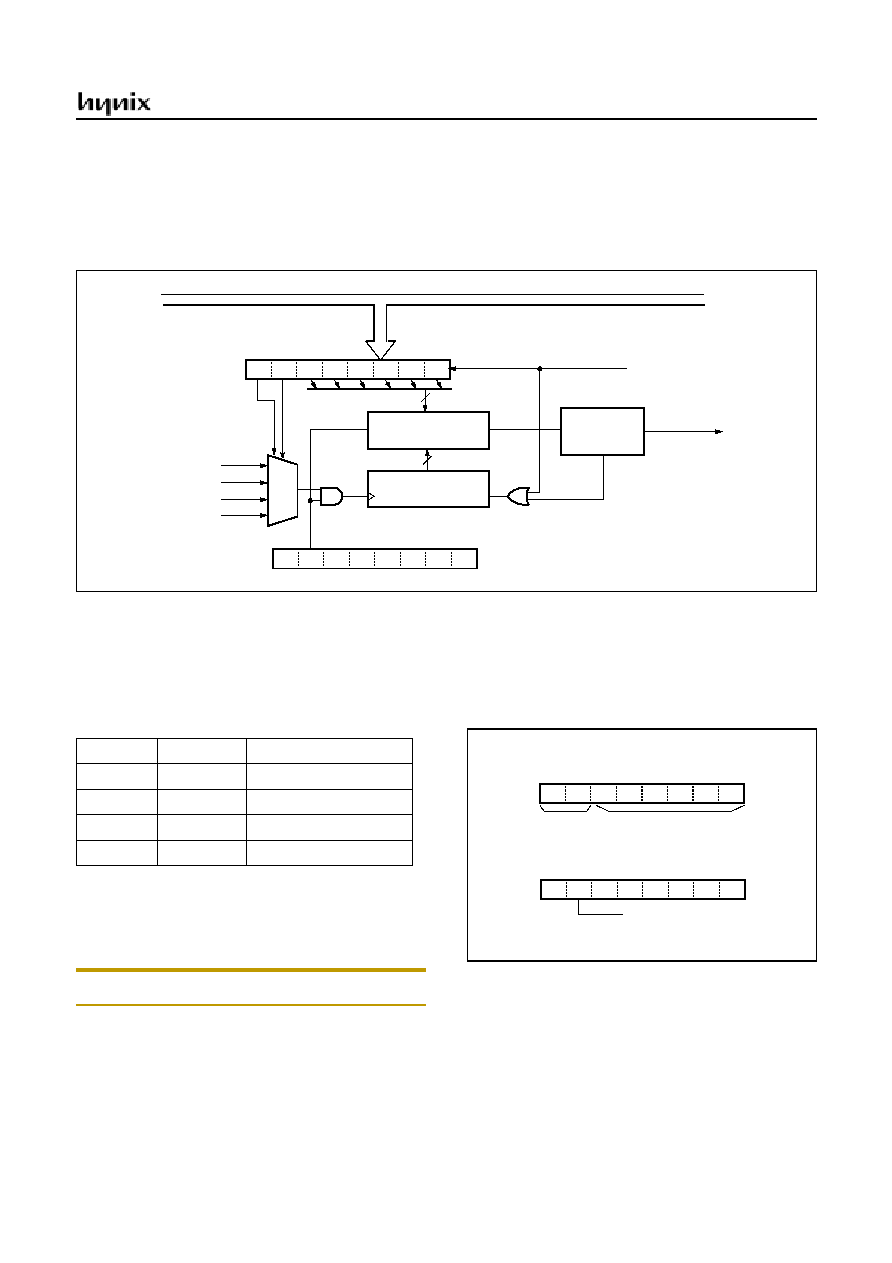
HMS81C4x60
November 2001 Ver 1.1
63
16. Buzzer driver
The Buzzer driver circuit is shown in Figure 16-1.
The Buzzer driver circuit consists of the 6bit counter, 6bit
comparator, Buzzer data register BUR(00EE
H
). The BUR
register controls source clock and output frequency.
The more details about registers are shown Figure 16-2 .
Figure 16-1 Block Diagram of Buzzer driver circuit
Control
The HMS81C4x60 contains a Buzzer driver module.
1. Select an input clock among PS7~PS10 by set the
BUCK1~0 of BUR.
2. Select output frequency by change the BU5~0.
Output frequency = 1 / (PSx
◊
BUy
◊
2) Hz.
x=7~10, y=5~0
See example Table 16-1.
Note: Do not select 00
H
to BU5~0. It means counter stop.
3. Set BUZ bit for output enable.
4. Output waveform is rectagle clock which has 50% duty.
5. You can use this clock for the other purposes.
Figure 16-2 Buzzer driver Registers
BUR [EE
H
]
BU5
BU4
BU3
BU2
BU1
BU0
6bit counter
Output
Generator
BUZZ
BUCK
MUX
PS7
PS9
PS8
PS10
BUCK
1
0
00
01
10
11
clear
6bit Comparator
clear
BUR write
6
6
Data Bus
8
PWMCR1
TM R1 BUZ
EN5
EN4
EN3
EN2
EN1
EN0
BUCK1
BUCK0
Clock source
0
0
PS7
0
1
PS8
1
0
PS9
1
1
PS10
Buzzer data Register
BUR
ADDRESS : 0EE
H
RESET VALUE : ???? ????
b
Input select
Buzzer count data
PWM control Register 1
PWMCR1
ADDRESS : 0EA
H
RESET VALUE : 0000 0000
b
R36/Buzz select
0: R36
1: Buzz output
W
W
W
W
W
W
W
W
RW
RW
RW
TM R1 BUZ
EN5
EN4
EN3
EN2
EN1
EN0
BUCK1 BUCK0 BU5
BU1
BU2
BU3
BU4
BU0
RW
RW
RW
RW
RW
HMS81C4x60
64
November 2001 Ver 1.1
BUR5~0
Output frequency (KHz)
Dec
Hex
PS7
(32
µ
S)
PS8
(64
µ
S)
PS9
(128
µ
S)
PS10
(256
µ
S)
1
2
3
4
5
6
7
8
9
10
11
12
13
14
15
16
17
18
19
20
21
22
23
24
25
26
27
28
29
30
31
32
33
34
35
36
37
38
39
40
41
42
43
44
45
46
47
48
49
50
51
52
53
54
55
56
57
58
59
60
61
62
63
01
02
03
04
05
06
07
08
09
0A
0B
0C
0D
0E
0F
10
11
12
13
14
15
16
17
18
19
1A
1B
1C
1D
1E
1F
20
21
22
23
24
25
26
27
28
29
2A
2B
2C
2D
2E
2F
30
31
32
33
34
35
36
37
38
39
3A
3B
3C
3D
3E
3F
31.25
15.625
10.436
7.813
6.25
5.208
4.464
3.907
3.472
3.125
2.841
2.604
2.404
2.242
2.083
1.953
1.838
1.736
1.644
1.562
1.438
1.420
1.359
1.302
1.25
1.202
1.158
1.116
1.078
1.042
1.008
0.976
0.947
0.919
0.893
0.868
0.845
0.822
0.801
0.781
0.762
0.744
0.727
0.710
0.694
0.679
0.665
0.651
0.638
0.625
0.613
0.601
0.590
0.579
0.568
0.558
0.548
0.539
0.530
0.521
0.512
0.504
0.496
62.50
31.25
20.872
15.626
12.50
10.416
8.928
8.814
6.942
6.25
5.682
5.208
4.808
4.484
4.166
3.906
3.676
3.472
3.288
3.124
2.876
2.840
2.718
2.604
2.50
2.404
2.316
2.232
2.156
2.084
2.016
1.952
1.894
1.838
1.786
1.736
1.690
1.644
1.602
1.562
1.524
1.488
1.454
1.420
1.388
1.358
1.33
1.302
1.276
1.25
1.226
1.202
1.18
1.158
1.136
1.116
1.096
1.078
1.06
1.042
1.024
1.008
0.992
125.0
62.5
41.744
31.252
25.0
20.832
17.858
17.628
13.884
12.5
12.364
10.416
9.616
8.968
8.332
7.812
7.342
6.944
6.576
6.248
5.752
5.680
5.436
5.208
5.0
4.808
4.632
4.464
4.302
4.168
4.032
3.904
3.788
3.676
3.552
3.472
3.380
3.288
3.204
3.124
3.048
2.978
2.908
2.840
2.776
2.706
2.66
2.604
2.542
2.5
2.452
2.404
2.36
2.316
2.272
2.232
2.192
2.156
2.12
2.084
2.048
2.016
1.984
250.0
125.0
83.488
62.504
50.0
41.664
35.716
35.256
27.768
25.0
24.728
20.832
19.232
17.936
16.664
15.624
14.684
13.888
13.152
12.496
11.504
11.360
10.872
10.416
10.0
9.616
9.262
8.928
8.604
8.336
8.064
7.808
7.576
7.352
7.104
6.944
6.760
6.576
6.408
6.248
6.096
5.956
5.816
5.680
5.552
5.412
5.320
5.208
5.184
5.0
4.904
4.808
4.720
4.632
4.544
4.464
4.384
4.312
4.24
4.168
4.096
4.032
3.968
Table 16-1 . Example for f
ex
=4MHz

HMS81C4x60
November 2001 Ver 1.1
65
17. On Screen Display (OSD)
The HMS81C4x60 can support 512 OSD chacters and font
size is used 12
◊10, 12◊12, 12◊14, 12◊16, 16◊18
. It can
support 48 character columns and 2 line buffers respective-
ly and also support full screen OSD when use interrupt.
Each characters have bit plane of 24bit and support at-
tribute with OSD line and full screen OSD respectively.
OSD circuit consists of the Position attribute register, Line
register, Full screen screen control register, I/O polarity
register, font ROM, VRAM, etc. On Screen Display block
diagram is shown in Figure 17-1 and the more details about
display characters are shown in Figure 17-2.
Figure 17-1 Block Diagram of On Screen Display circuit
L1ATTR [AF0
H
]
OSD Control
Circuit
OSDLN [AE5
H
]
OSDCON1 [AE0
H
]
OSDCON2 [AE1
H
]
Line 1,2 Attribute,
Position register
Line register
Full screen control
Display On/Off Control
register
L1VPOS [AF1
H
]
L2ATTR [AF3
H
]
L2VPOS [AF4
H
]
LHPOS [AE6
H
]
Horizontal position register
VRAM
Font ROM
DAC
Color Pallet
OSD Generation Circuit
Output
Control
Circuit
Synchronization
Circuit
HSYNC
VSYNC
R
G
B
YS
YM
dot clock
Xin
PLL
FDWSET [AE3
H
]
Field detection register
EDGECOL [AE4
H
]
Edge color register
OSDCON3 [AE2
H
]
I/O Porarity Rigister
register
HMS81C4x60
66
November 2001 Ver 1.1
Figure 17-2 OSD Character Font Example
[12
◊
10 Character Font]
[12
◊
12 Character Font]
[12
◊
14 Character Font]
[12
◊
16 Character Font]
[16
◊
18 Character Font]
OSD background shadow
Foreground Character
- 512 color (8 pallet)
- color selecting : VRAM n-character bit 19~16
Background
- 512 color (8 pallet)
- color selecting : VRAM n-character bit 23~20
Foreground Character outline
- setting by LnATTR register
- color selecting : EDGECOL register
Character shadow
- setting by LnATTR register and VRAM n-character bit 9
- color selecting : EDGECOL register
Background shadow color
- setting by VRAM n-character bit 15~12
- color selecting : EDGECOL register
- 512 color (8 pallet)
- Character flash
- background underline
- italic (only 12
◊
12 mode can be supported)
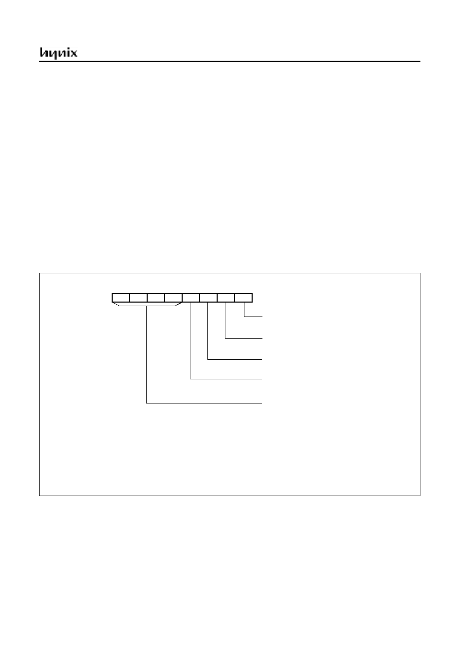
HMS81C4x60
November 2001 Ver 1.1
67
17.1 Feature of OSD
The Feature of OSD shown in below.
- Font pixel matrix
: 12
◊10, 12◊12, 12◊14, 12◊16, 16◊18
dots
- The number of font pattern
: 512 fonts
- Display ability
: 48Character
◊
n lines (multilined by OSD interrupt)
- 8 foreground pallet of 512 colors for each character
- 8 background pallet of 512 colors for each character
- Full screen 8 background color
- Character size
: 3 fonts(2 times, 1.5 times, 1 times)
- Progressive scan line switch
- Attribute
: Outline, Shadow, Rounding
- RGB DAC
: 8 level each color
- Display clock frequency
: 12MHz ~ 64MHz
17.2 OSD Registers
Figure 17-3 OSD Control Registers - 1
OSDCON1
bit 0: STOCK
It stop or start OSD clock. If oscillation is stoped, IC's
power consumption is decreased.
bit 1: DDCLK
If you set this bit to 1, OSD input clock is divided by two ,
than it makes OSD horisontal image size as doubled.
bit 2: DLINE
If you set this bit to 1, OSD vertical scan counter input
clock is doubled from normal state. It makes OSD vertical
INITIAL VALUE: 0000 0000
b
ADDRESS: 0AE0
H
MSB
LSB
Stop OSD clock
Double dot clock mode
R/W
R/W
R/W
R/W
R/W
R/W
R/W
R/W
D D C LK
DLIN E
P R S C N
FS B C 0
FS B C 1
FS B C 2
FS B C 3
S TO C K
OSDCON1
0 :Release OSD clock
0 : Normal
1 : Double
1 : Stop OSD clock
Double scan line mode
0 : Normal
1 : Double
Progressive scan line mode
0 : Interace mode
1 : Progressive mode
Full screen background color register
0000 : Transparency
0001 : Half blank
0010 : white
0011 : Black
0111 ~ 0100 : Reserved
1000 : color 0
1001 : color 1
1010 : color 2
1011 : color 3
1100 : color 4
1101 : color 5
1110 : color 6
1111 : color 7
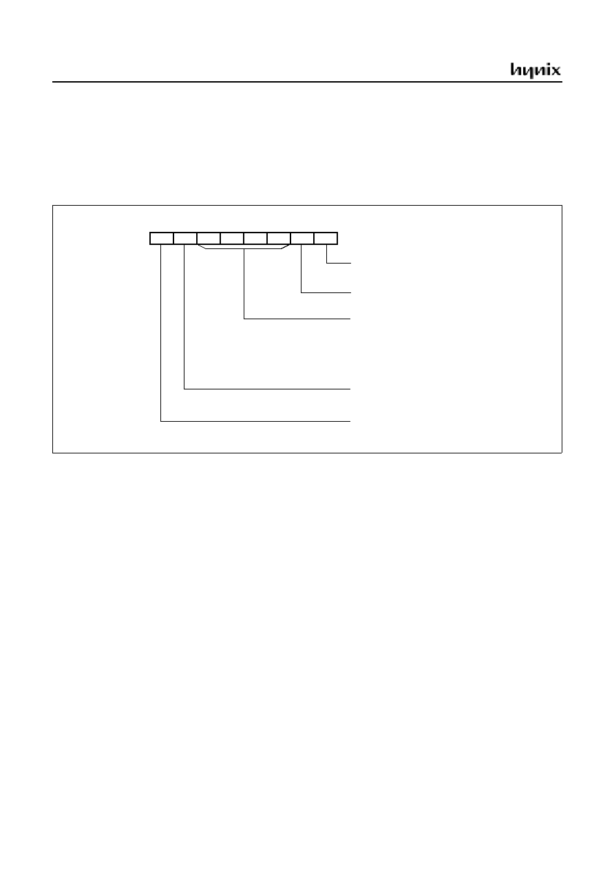
HMS81C4x60
68
November 2001 Ver 1.1
image size as doubled.
bit 3: PRSCN
It control progressive scan line mode.
bit clear than interace mode and bit set than processive
mode.
bit 7~4: FSBC3 ~ FSBC0
It controls full screen background color as figure shows.
NOTE:
Data slicer operate when OSDCON1.PRSCN(0AE0.3) bit of OSD register is
cleared. Namely, it operate interace scan display mode.
Figure 17-4 OSD Control Register - 2
OSDCON2
bit 0: OSDON
It controls OSD, Full screen background at once. It does
not affect anything to Vsync interrupt and OSD interrupt,
etc.
bit 1: ONL
It controls OSD line1 and line2 on/off. If its value is 1,
OSD line is on.
bit 2 ~ 5: FS0 ~ FS3
It controls OSD font size.
bit 6: OBGW
It controls dot background width. Default width is 12dots.
If its value is set, 2 dots (background color) are added both
left and right side of character.
bit 7: FLRAT
It controls OSD flash rate when closed caption decoder is
used. Bit clear than 32 Vsync is one period and bit set than
64 Vsync is one period.
INITIAL VALUE: 0000 0000
b
ADDRESS: 0AE1
H
MSB
LSB
On/off of all OSD
On OSD line1 and line2
R/W
R/W
R/W
R/W
R/W
R/W
R/W
R/W
O LN
FS 0
FS 1
FS 2
FS 3
O B G W
FLA R T
O S D O N
OSDCON2
0 :Off
0 : Off OSD line
1 : On OSD line
1 : On
Font size
12/14 dot background width of 1 OSD character
0 : 12 dot
1 : 14 dot
Flash rate when closed caption decoder is used
0 : 32 Vsync is one period
1 : 64 Vsync is one period
0000 : 12
◊
16
0001 : 12
◊
14
0010 : 12
◊
12
0011 : 12
◊
10
0111 ~ 0100 : Reseved
1000 : 16
◊
18
1111 ~ 1001 : Reserved

HMS81C4x60
November 2001 Ver 1.1
69
Figure 17-5 I/O Polarity(Initial) Register
OSDCON3
bit7~0 : SELCK1, SELCK0, ONDAC, POLRG, POLYM,
POLYS, POLHS, POLVS
It controls Hsync/Vsync polarity, YS/YM polarity, RGB
polarity, RGB DAC on/off and select dot clock.
FDWSET
FDWSET (Field Detection Window Setting) register de-
tects the begin of Vsync(Vertical Sync.) signal and distin-
guishs its current field is Even field or Odd field.
The region of FMIN[2:0] ~ FMAX[3:0] is field detection
window.
FMAX[3:0] can divide the region between Hsync(Hori-
zontal Sync.) by 16 windows. You can assume there is 4
bit horizontal counter, for example HCOUNT[3:0](hptr[10
:7]) which count 0~15.
INITIAL VALUE: 0000 0000
b
ADDRESS: 0AE2
H
MSB
LSB
Vsync polarity
Hsync polarity
W
W
W
W
W
W
W
W
SELCK1
OSDCON3
0 : Active low
0 : Active low
1 : Active high
1 : Active high
YS polarity
RGB pin polarity
0 : Active low
1 : Active high
On/Off of RGB DAC
0 : Off
1 : On
0 : Active low
1 : Active high
YM polarity
0 : Active low
1 : Active high
Select dot clock
00 : Clock from DLL
01 : Clock from LC OSC for EVA only
10 : Clock 1 for test
11 : Reserved
POLHS
POLVS
POLYS
POLYM
POLRG
ONDAC
SELCK2
INITIAL VALUE: 0111 1010
b
ADDRESS: 0AE3
H
MSB
LSB
Field Detection Min. Pointer
Field Detection Polarity
W
W
W
W
W
W
W
W
FM IN 1
F M IN 2
D B FLG
FM A X 0
FM A X 1
FM A X 2
FM A X 3
FM IN 0
FDWSET
0 : Masking between Min. and Max.
1 : Detect between Min. and Max.
Field Detection Max. Pointer
Field Detection Window:
( {1'b0, (FMIN2 ~ FMIN0)} < hptr[10:7] < (FMAX3 ~ FMAX0))
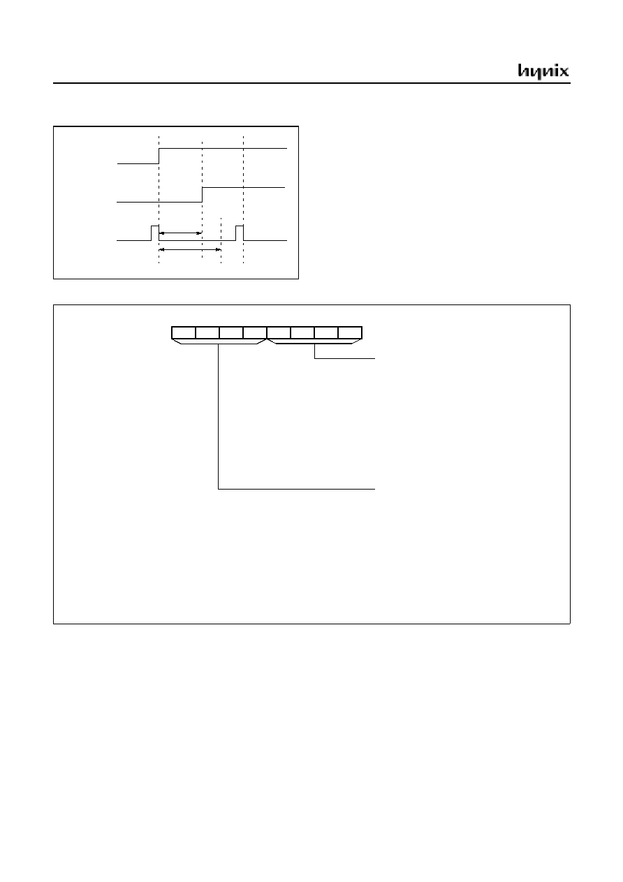
HMS81C4x60
70
November 2001 Ver 1.1
Figure 17-6 FDWSET detection region
If the start of Vsync is detected at the window, next field is
even. Else if Vsync is detected another region of the win-
dow, next field is odd.
It means start of Vsync is detected during FMIN[2:0] <
HCOUNT[3:0] < FMAX[3:0] and DBFLG value is 0, it
distinguish odd field.
And, start of Vsync is detected during FMIN[2:0] <
HCOUNT[3:0] < FMAX[3:0] and DBFLG value is 1, it
distinguish even field.
FMIN[2:0], FMAX[3:0] are compared with the horizontal
counter in OSD block.
Figure 17-7 Character, Window color Register
EDGECOL
bit 7 ~ bit 0 : EDG1C0,EDG1C1,EDG1C2,EDG1C3
EDG2C0,EDG2C1,EDG2C2,EDG2C3
It control shadow color, outline color and edge color.
Low 4 bits controls edge 1 shadow, outline color and high
4 bits controls edge 2 shadow, outline color.
HSync
Ex1: VSync(Odd)
Ex2: VSync(Even)
FMIN
FMAX
INITIAL VALUE: 1000 0111
b
ADDRESS: 0AE4
H
MSB
LSB
R/W
R/W
R/W
R/W
R/W
R/W
R/W
R/W
EDG2C3
EDGECOL
Edge 2 color of shadow, outline, edge
Edge 1 color of shadow, outline, edge
0000 : Transparency
0001 : Reserved
0010 : white
0011 : Black
0100 : Same as foreground character color
0111 ~ 0101 : Reserved
1000 : color 0
1001 : color 1
1010 : color 2
1011 : color 3
1100 : color 4
1101 : color 5
1110 : color 6
1111 : color 7
0000 : Transparency
0001 : Reserved
0010 : white
0011 : Black
0100 : Same as foreground character color
0111 ~ 0101 : Reserved
1000 : color 0
1001 : color 1
1010 : color 2
1011 : color 3
1100 : color 4
1101 : color 5
1110 : color 6
1111 : color 7
EDG2C2 EDG2C1 EDG2C0 EDG1C3 EDG1C2 EDG1C1 EDG1C0
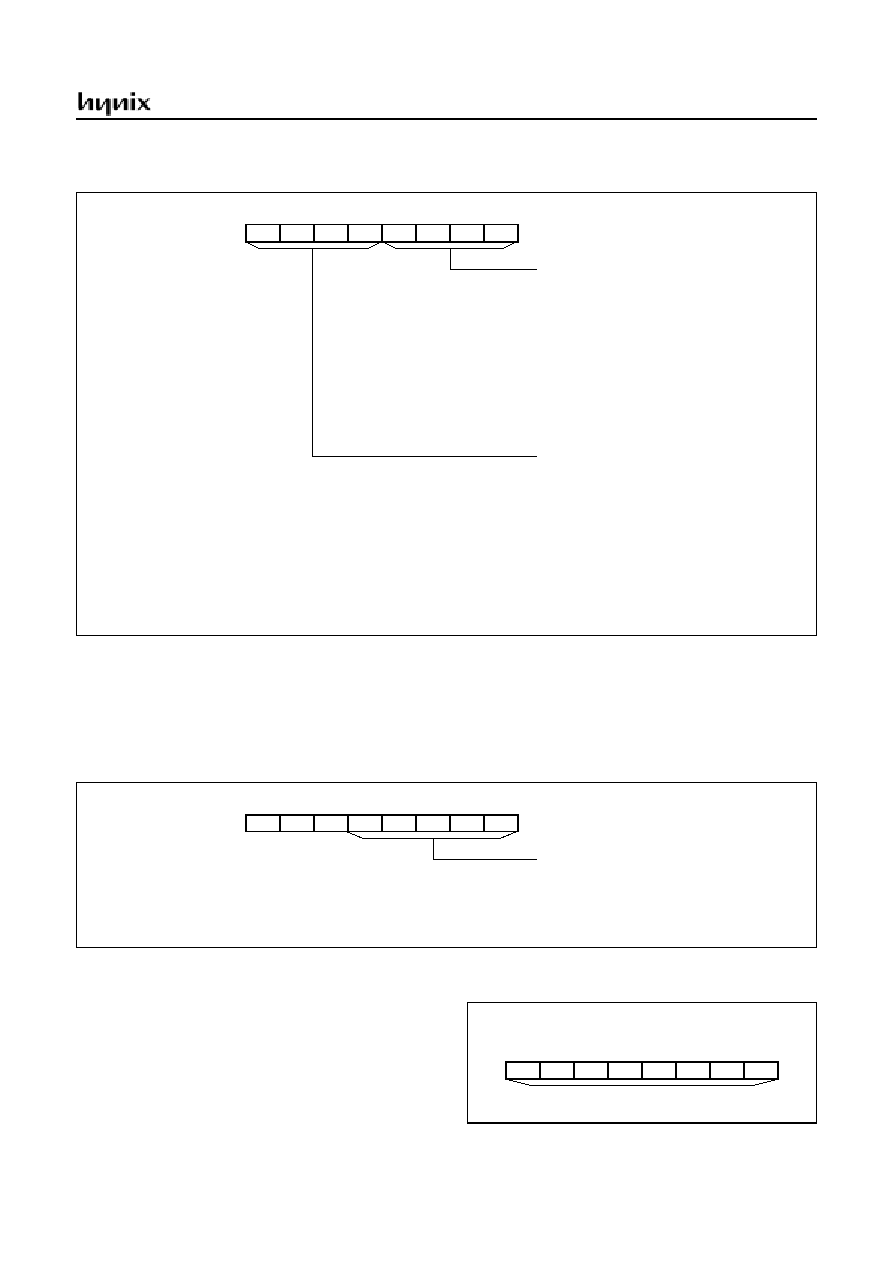
HMS81C4x60
November 2001 Ver 1.1
71
Figure 17-8 Scroll window color Register
CHEDCL
bit 7 ~ bit 0 : SHEC0,SHEC1,SHEC2,SHEC3
WINC0,WINC1,WINC2,WINC3
It controls foreground shadow and outline edge color and
scroll window background color.
Low 4 bits controls scroll window background color and
high 4 bits controls foreground shadow outline edge color.
Figure 17-9 OSD Line Register
OSDLN
bit 4 ~ bit 0 : VLR4 ~ VLR0
It shows current display OSD line from 1 to 31.
INITIAL VALUE: Undefined
ADDRESS: 0AE5
H
MSB
LSB
W
W
W
W
W
W
W
W
S H E C 1
S H E C 2
S H E C 3
W IN C 0
W IN C 1
W IN C 2
W IN C 3
S H E C 0
CHEDCL
Scroll window background color
Foreground shadow, outline edge color
0000 : Transparency
0001 : Reserved
0010 : white
0011 : Black
0100 : Same as foreground character color
0111 ~ 0101 : Reserved
1000 : color 0
1001 : color 1
1010 : color 2
1011 : color 3
1100 : color 4
1101 : color 5
1110 : color 6
1111 : color 7
0000 : Transparency
0001 : Reserved
0010 : White
0011 : Black
0111 ~ 0100 : Reserved
1000 : Color 0
1001 : Color 1
1010 : Color 2
1011 : Color 3
1100 : Color 4
1101 : Color 5
1110 : Color 6
1111 : Color 7
INITIAL VALUE: ---0 0000
H
ADDRESS: 0AE6
H
MSB
LSB
R
R
R
R
R
R
R
R
V LR 1
V LR 2
V LR 3
V LR 4
-
-
-
V LR 0
OSDLN
OSD line being displayed
00000 : Not displayed any OSD line yet after Vsync
00001 : 1st line OSD being displayed
.......
.......
11111 : 31st line OSD being displayed
MSB
LSB
W
W
W
W
W
W
W
W
LH 1
LH2
LH3
LH4
LH5
LH6
LH7
LH 0
LHPOS
INITIAL VALUE: Undefined
ADDRESS: 0AE7
H
OSD Line Horizontal Position 00
H
~ FF
H
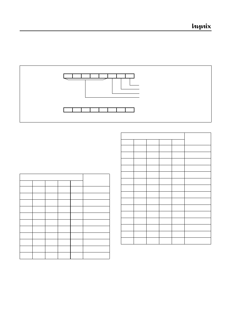
HMS81C4x60
72
November 2001 Ver 1.1
Figure 17-10 OSD Line Horizontal Position Register
LHPOS
bit 7 ~ bit 0 : LH7 ~ LH0
It control OSD line horizontal position. Position value
from 00h to FFh.
Figure 17-11 DLL mode Register
DLLMOD
bit 2 ~ 0 : If you set this bit to 1, the status is changed test
mode.
bit 7 ~ bit 3 : DCKF4 ~ DCKF0
It control dot clock frequency.
Dot clock frequency is as below.
Table 17-1 Dot Clock Frequency (f
ex
=4Mhz)
INITIAL VALUE: 0000 0000
H
ADDRESS: 0AE8
H
MSB
LSB
W
W
W
W
W
W
W
W
-
-
D C K F0
D C K F1
D C K F2
D C K F3
D C K F4
-
DLLMOD
1 : OSD test mode
1 : Dll test mode
1 : Reset clock count test mode
Dot clock frequency
INITIAL VALUE: --00 0000
H
ADDRESS: 0AE9
H
MSB
LSB
R
R
R
R
R
R
R
R
-
-
-
-
-
-
-
-
DLLTST
Value
Frequency
DCKF4
DCKF4
DCKF4
DCKF4
DCKF4
0
0
0
0
0
stop dll clock
0
0
0
0
1
reserved
0
0
0
1
0
reserved
0
0
0
1
1
64.00MHz
0
0
1
0
0
51.20MHz
0
0
1
0
1
42.67MHz
0
0
1
1
0
36.57MHz
0
0
1
1
1
32.00MHz
0
1
0
0
0
28.44MHz
0
1
0
0
1
25.60MHz
0
1
0
1
0
23.27MHz
0
1
0
1
1
21.33MHz
0
1
1
0
0
19.69MHz
0
1
1
0
1
18.29MHz
0
1
1
1
0
17.07MHz
0
1
1
1
1
16.00MHz
1
0
0
0
0
15.05MHz
1
0
0
0
1
14.22MHz
1
0
0
1
0
13.47MHz
1
0
0
1
1
12.80MHz
1
0
1
0
0
12.19MHz
1
0
1
0
1
11.63MHz
1
0
1
1
0
11.13MHz
1
0
1
1
1
10.67MHz
1
1
0
0
0
reserved
1
1
0
0
1
reserved
Value
Frequency
DCKF4
DCKF4
DCKF4
DCKF4
DCKF4

HMS81C4x60
November 2001 Ver 1.1
73
Figure 17-12 OSD line 1 attribute register
L1ATTR
bit 0 : L1V8
It is equivalent to L1VPOS's most significant bit(bit 8).
See more details in L1VPOS.
bit 1: FSC1
It selects character outline and shadow color. If it is 1, it se-
lect EDGE2 color of EDGECOL register. Or not, it select
EDGE1 color. According to EDGECOL register and this
bit character and shadow colors are selected simulteneous-
ly
bit 3~2: CSZ11~CSZ10
It controls OSD character's size ( normal, 1.5 times, 2
times). You can use this register and DDCLK, DLINE bit,
horizontal / vertical size can be controlled (x1, x1.5, x2).
bit 4: ENSH1
It enables line 1's character(foreground) shadow.
bit 5: ENOL1
It enables line 1's character(foreground) outline.
bit 6: WDSL1
It shows thickness of line 1's shadow and outline.This bit
is set than one dot and bit clear is proportional to character
size. If only character size is 2 times, 2 times per vertically
and horizontally. In case 1 dot width would be enable.
bit 7: OBGH1
It controls character's background height. Default height is
16dots. If its value is set, 2 dots (background color) are
added both top and bottom side of character.
INITIAL VALUE: 0000 0000
H
ADDRESS: 0AEA
H
MSB
LSB
W
W
W
W
W
W
W
W
FS C 1
C S Z10
C S Z11
E N S H 1
E N O L1
W D S L1
O B G H 1
L1V 8
L1ATTR
OSD line 1 vertical position (bit 8)
Size of character
Enable/disable of shadow
00 : Normal
01 : 1.5 times
10 : 2 times
11 : Reserved
0 : Disable
1 : Enable
Enable/disable of outline
0 : Disable
1 : Enable
Width of shadow, outline
0 : 1 dot
1 : Proportional to character size
OSD chraracter background height
0 : font height
1 : font height + 2
Foreground shadow or outline color select
0 : Edge 1 color
1 : Edge 2 color
HMS81C4x60
74
November 2001 Ver 1.1
L1EATR
It shows OSD line 1 extend attribute register.
L1VPOS
It shows OSD line 1's vertical position in 9bit format
(LIV8 + L1VPOS, 000 ~ 1FF
H
).
L2ATTR
It shows OSD line 2's attributes. Its function is the same as
L1ATTR.
L2EATR
It shows OSD line 2's extened attribute register.
L2VPOS
It shows OSD line 2's vertical position. Its function is the
same as L1VPOS.
INITIAL VALUE: Undefined
ADDRESS: 0AEB
H
MSB
LSB
W
W
W
W
W
W
W
W
S E L1IT
S E L1FL
S E L1O W
S E L1U L
-
-
-
S E L1S H
L1EATR
Select shadow/round of line 1 each character when
Select italic/upper edge of line 1 each character.
Select flash/left edge of line 1 character when
Select OSD/window when display. If this bit is 0,
Select underline /lower edge of line 1 each character
0 : Underline
1 : Lower edge line
VRAM.ENRND is set.
0 : round character
1 : shadow character
Italic character can be displayed only when character
size is 1, 1.5 times, and VRAM.BSU is set.
0 : Upper edge character
1 : Italic character
VRAM.BSL is set.
0 : Left edge character
1 : Flash
background window would be displayed.
0 : Background window selected
1 : OSD line selected
MSB
LSB
W
W
W
W
W
W
W
W
LIV 1
LIV 2
LIV 3
LIV 4
LIV 5
LIV 6
LIV 7
LIV 0
L1VPOS
INITIAL VALUE: Undefined
ADDRESS: 0AEC
H
OSD line 1 vertical position 000
H
~ 1FF
H
MSB
LSB
W
W
W
W
W
W
W
W
F S C 2
C S Z 21
C S Z 22
E N S H 2
E N O L2
W D S L2
O B G H 2
L2V 2
L2ATTR
INITIAL VALUE: Undefined
ADDRESS: 0AED
H
MSB
LSB
W
W
W
W
W
W
W
W
S E L2IT
S E L2F L
S E L2O W
S E L2UL
-
-
-
S E L2S H
L2EATR
INITIAL VALUE: Undefined
ADDRESS: 0AEE
H
MSB
LSB
W
W
W
W
W
W
W
W
L2V 1
L2V 2
L2V 3
L2V 4
L2V 5
L2V 6
L2V 7
L2V 0
L2VPOS
INITIAL VALUE: Undefined
ADDRESS: 0AEF
H

HMS81C4x60
November 2001 Ver 1.1
75
WINSH
It shows OSD scroll window start horizontal position.
WINSY
It shows OSD scroll window start vertical position.
WINEH
It shows OSD scroll window end horizontal position.
WINEY
It shows OSD scroll window end vertical position.
VCNT
It shows Vsync count register and counted by pixel clock.
VCNT counter clock start at Vsync start edge.
HCNT
It shows Hsync count register and counted by pixel clock.
HCNT counter clock start at Hsync start edge.
CULTAD
It shows normal and test mode and 1.5 times mode.
MSB
LSB
W
W
W
W
W
W
W
W
W IN SH 7
WINSH
INITIAL VALUE: Undefined
ADDRESS: 0AF0
H
OSD scroll window start horizontal position
W IN SH 6 W IN SH 5 W IN SH 4 W IN SH 3 W IN SH 2 W IN SH 1 W IN SH 0
MSB
LSB
W
W
W
W
W
W
W
W
W INSY7
WINSY
INITIAL VALUE: Undefined
ADDRESS: 0AF1
H
OSD scroll window start vertical position
W INSY6 W INSY5 W INSY4 W INSY3 W INSY2 W INSY1 W INSY0
MSB
LSB
W
W
W
W
W
W
W
W
W IN EH 7
WINEH
INITIAL VALUE: Undefined
ADDRESS: 0AF2
H
OSD scroll window end horizontal position
W IN EH 6 W IN EH 5 W IN EH 4 W IN EH 3 W IN EH 2 W IN EH 1 W IN EH 0
MSB
LSB
W
W
W
W
W
W
W
W
W INEY7
WINEY
INITIAL VALUE: Undefined
ADDRESS: 0AF3
H
OSD scroll window end vertical position
W INEY6 W INEY5 W INEY4 W INEY3 W INEY2 W INEY1 W INEY0
MSB
LSB
R
R
R
R
R
R
R
R
V C N T 6
V C N T6
V C N T6
V C N T6
V C N T6
V C N T6
V C N T6
F LD ID
VCNT
INITIAL VALUE: Undefined
ADDRESS: 0AF4
H
Current scan line line vertical position [6:0]
Current display field
0 : Odd field
1 : Even field
MSB
LSB
R
R
R
R
R
R
R
R
H C N T1
H C N T 2
H C N T 3
H C N T 4
H C N T 5
H C N T 6
H C N T 7
H C N T0
HCNT
INITIAL VALUE: Undefined
ADDRESS: 0AF5
H
Horizontal counter hptr[10:3]
MSB
LSB
W
W
W
W
W
W
W
W
F IL15
-
-
-
-
-
-
-
CULTAD
INITIAL VALUE: Undefined
ADDRESS: 0AF9
H
1.5 times character mode
0 : line double mode 1.5 times
1 : field interleaving mode 1.5 times
Normal/Test mode select
00 : Normal mode
01 ~ 11 : Test mode
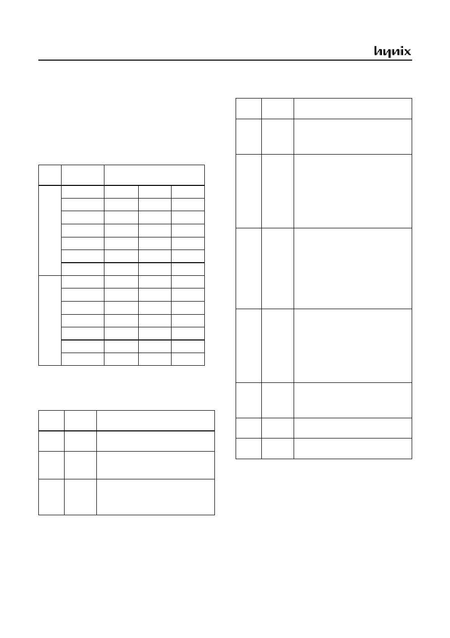
HMS81C4x60
76
November 2001 Ver 1.1
17.3 VRAM
VRAM contains a OSD line buffer, 48 character's at-
tributes.
Each character's attribute is constructed with 3 bytes, it
contains color data for background, shadow, outline, char-
acter and character number ( 000
H
~ 1FF
H
, 512 characters
), etc.
Table 17-3 VRAM attribute
Line
No.
Character
add. No.
Address (bit 47~0)
Hexa decimal
1
1
A80
A40
A00
2
A81
A41
A01
3
A82
A42
A02
:
:
:
:
46
AAD
A6D
A2D
47
AAE
A6E
A2E
48
AAF
A6F
A2F
2
1
B80
B40
B00
2
B81
B41
B01
3
B82
B42
B02
:
:
:
:
46
BAD
B6D
B2D
47
BAE
B6E
B2E
48
BAF
B6F
B2F
Table 17-2 VRAM memory map
Bit
No.
Name
Function
00~08
CG8
~CG0
Character font code
1FFh ~ 000h
09
ENRND
Round enable/disable
0 : disable
1 : enable
0A
BSCUL
Edge color of upper and left
background shadow edge
0 : edge 1 color
1 : edge 2 color
0B
BSCDR
Edge color of lower and right
background shadow edge
0 : edge 1 color
1 : edge 2 color
0C
BSU
Background shadow upper eddge
control/italic depend on
LxEATR.SELxIT
0 : disable
1 : enable
if(LxEATR.SELxIT == 0) background
shadow upper edge enable
else(LxEATR.SELxIT == 1) italic
enable
0D
BSD
Background shadow lower edge
control/underline depend on
LxEATR.SELxUL
0 : disable
1 : enable
if(LxEATR.SELxUL == 0)
background shadow lower edge
enable
else(LxEATR.SELxUL ==
1)underline enable
0E
BSL
Background shadoww left edge
control/flash(blInking) depend on
LxEATR.SELxFL
0 : disable
1 : enable
if(LxEATR.SELxFL == 0) background
shadow left edge enable
else(LxEATR.SELxFL == 1)
flash(flicking) enable
0F
BSR
Background shadow right edge
control
0 : disable
1 : enable
10~13
FC3
~FC0
Foreground color for character (11
colors)
14~17
BC3
~BC0
Background color for character (12
colors)
Bit
No.
Name
Function
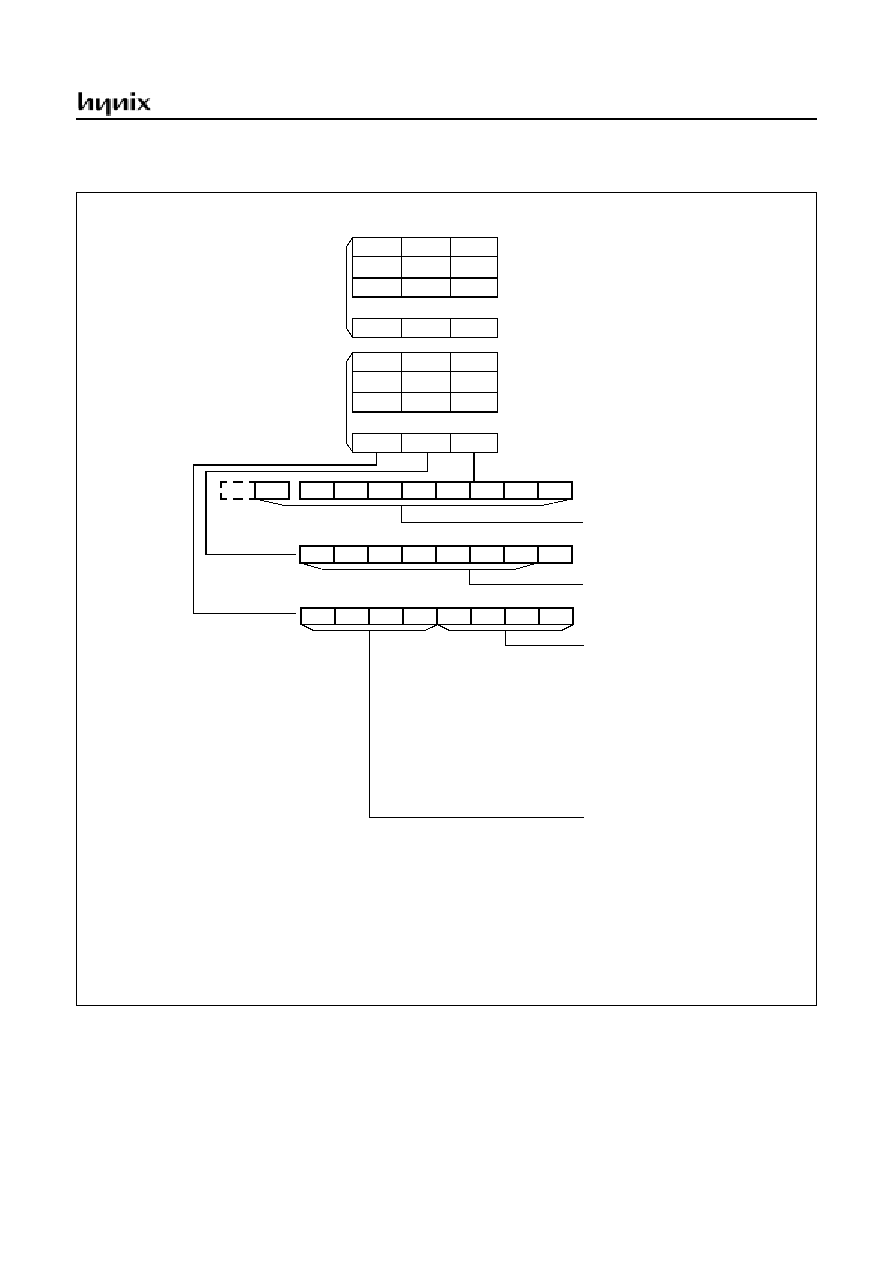
HMS81C4x60
November 2001 Ver 1.1
77
0A80 0A40 0A00
0A81 0A41 0A01
0A82 0A42 0A02
: : :
0AAF 0A6F 0A2F
LINE 1
(page A)
Character 1 Attr.
Character 2 Attr.
Character 3 Attr.
0B80 0B40 0B00
0B81 0B41 0B01
0B82 0B42 0B02
: : :
0BAF 0B6F 0B2F
LINE 2
(page B)
Character 1 Attr.
Character 2 Attr.
Character 3 Attr.
Character 48 Attr.
Character 48 Attr.
E N R N D
B S C U L
B S C D R
B S U
B S D
B S L
B S R
C G 8
C G 1
C G 2
C G 3
C G 4
C G 5
C G 6
C G 7
C G 0
RESET VALUE: Undefined
Composition of VRAM
Character font address (512 fonts)
C G 8
see table 17-3 VRAM attribute
F C 1
FC 2
FC 3
B C 0
B C 1
B C 2
B C 3
FC 0
Character color select (11 characters)
0000 : Transparency
0001 : Reserved
0010 : White
0011 : Black
0111 ~ 0100 : Reserved
1000 : Color 0
1001 : Color 1
1010 : Color 2
1011 : Color 3
1100 : Color 4
1101 : Color 5
1110 : Color 6
1111 : Color 7
Background color select (12 characters)
0000 : Transparency
0001 : Reserved
0010 : White
0011 : Black
0111 ~ 0100 : Reserved
1000 : Color 0
1001 : Color 1
1010 : Color 2
1011 : Color 3
1100 : Color 4
1101 : Color 5
1110 : Color 6
1111 : Color 7
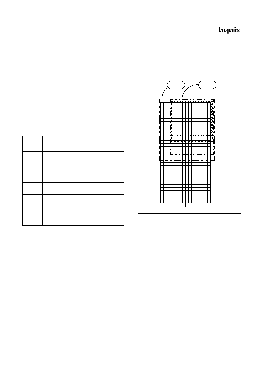
HMS81C4x60
78
November 2001 Ver 1.1
17.4 Character ROM
The HMS81C4x60 Character ROM are used 512 types of
Font Dot Pattern data. As displayed one character, need 12
◊
10 ~ 16
◊
18bits Dot Pattern data.
1. Each horizontal data (12dots) needs 2bytes ROM.
2. One character is constructed with 16 horizontal data to
vertically. As a result, one character needs 32bytes (2
◊
16
bytes).
3. HMS81C4x60 contains 512 characters. Total Font
ROM memory size is calculated as 16,384bytes ( 32bytes
/ character
◊
512 characters )
4. Font ROM memory is located from 10000
H
~ 17FFF
H
,
this memory can not be accessed by user program.
5. A character's address and dot position in font ROM is
described in Figure 17-13.
Figure 17-13 Character Dot Pattern
Charact
er code
Address range
Upper 8bit
Lower 8bit
000
H
14000
H
~ 14011
H
10000
H
~ 10011
H
001
H
14020
H
~ 14031
H
10020
H
~ 10031
H
002
H
14040
H
~ 14051
H
10040
H
~ 10051
H
:
:
:
xyz
H
(14000H + xyz0H) ~
(14000H + 2*xyzFH)
(10000H + xyz0H) ~
(10000H + 2*xyzFH)
:
:
:
1FD
H
17FA0
H
~ 17FB1
H
13FA0
H
~ 13FD1
H
1FE
H
17FC0
H
~ 17FD1
H
13FC0
H
~ 13FD1
H
1FF
H
17FE0
H
~ 17FF1
H
13FE0
H
~ 13FF1
H
Table 17-4 Font ROM memory map
Right
address
14060
14061
Left
address
14062
14063
14064
14065
14066
14067
14068
14069
1406A
1406B
1406C
1406D
1406E
1406F
14070
14071
14072
14073
14074
14075
14076
14077
14078
14079
1407A
1407B
1407C
1407D
1407E
1407F
10060
10061
10062
10063
10064
10065
10066
10067
10068
10069
1006A
1006B
1006C
1006D
1006E
1006F
10070
10071
10072
10073
10074
10075
10076
10077
10078
10079
1007A
1007B
1007C
1007D
1007E
1007F
12
◊
14
16
◊
18

HMS81C4x60
November 2001 Ver 1.1
79
17.5 Color Look Up Table
Figure 17-14 Color look up table
[Example] Color data table
Color_example_table:
db 0000_0000b ;color 0 = Gray
db 0000_0011b ;color 1 = Red
db 0010_1011b ;color 2 = Green
;
db 0000_0000b ;color 3 = Yellow
db 0000_0101b ;color 4 = Blue
db 0100_1101b ;color 5 = Magenta
;
db 0000_0000b ;color 6 = Cyan
db 1001_0001b ;color 7 = half blue
db 1111_0001b
<0AD0
H
>
RED0
<0AD1
H
>
RED1
<0AD2
H
>
RED2
<0AD3
H
>
GREEN0
<0AD4
H
>
GREEN1
<0AD5
H
>
GREEN2
<0AD6
H
>
BLUE0
<0AD7
H
>
BLUE1
<0AD8
H
>
BLUE2
W
W
W
W
W
W
W
W
7
6
5
4
3
2
1
0
B72
B62
B52
B42
B32
B22
B12
B02
R07
R60
R50
R40
R30
R20
R10
R00
R71
R62
R51
R41
R31
R21
R11
R01
R72
R62
R52
R42
R32
R22
R12
R02
G70
G60
G50
G40
G30
G20
G10
G00
G71
G61
G51
G41
G31
G21
G11
G01
G72
G62
G52
G42
G32
G22
G12
G02
B70
B60
B50
B40
B30
B20
B10
B00
B71
B61
B51
B41
B31
B21
B11
B01
Composition of color 3
Red : {R02,R01,R00}
Green : {G02,G01,G00}
Blue : {B02,B01,B00}
Composition of color 2
Composition of color 1
Composition of color 0
Composition of color 4
Composition of color 5
Composition of color 6
Composition of color 7
RESET VALUE : Undefined

HMS81C4x60
80
November 2001 Ver 1.1
18. DATA SLICER
HMS81C4x60 supports Closed Caption decoding standard
with 0.5MHz data rate. Also it can capture 4 horizontal
lines information per frame, because it has 4 horozontal
lines capture memory. It is able to select even or odd field
at one field interval. Data Slicer captures caption informa-
tion from line 21 in vertical blanking interval of CVBS,
and stores these data to buffer memory.
18.1 Data Slicer Circuit
Figure 18-1 shown the data slicer circuit.
Figure 18-1 Data Slicer Circuit
CVBS signal is entered to CVBS pin via 0.47uF capacitor.
The black level of signal is about 2V. SCAP pin is connect-
ed to external 560pF capacitor which adjust the referance
voltage of comparator. Its slicer level is adapted to input
signal.
18.2 Configuration of Data Slicer
Figure 18-2 shows the block diagram of the Data Slicer.
Figure 18-2 Data Slicer Block Diagram
This data slicer block separates caption information from
CVBS signal. Data slicer composes high speed comparator
and on-chip low pass filter. The output data of comparator
is stored in memory through the filter and memory inter-
face controller, which should be decoded to caption data
by software. Slicer memory addressed 600h ~ 6FFh.
SCAP
CVBS
560pF
0.47uF
HMS81C4x60
Run-in key timing
Sync-tip timing
Data capture
timing
Data
Filter
Memory
Interface
Controller
Slicer
Memory
Reference
Voltage
CVBS
Timing
Controller
CPU control
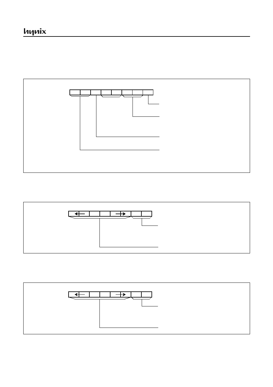
HMS81C4x60
November 2001 Ver 1.1
81
18.3 Slicer Registers
Slicer Control Register
Slicer Control Register is the specific control register,
which select operating frequency of the slicer, slicer de-
coding method and switch slicer on/off.
Figure 18-3 Slicer Control Register
Slicer Information Register 0
Slicer Information Register 0 selects even or odd field
buffer of line 0 and slicer line 0 position. Also it is used to
select line number in Vertical blanking interval.
Figure 18-4 Slicer Information Register 0
Slicer Information Register 1
Slicer Information Register 1 selects even or odd field
buffer of line 1 and slicer line 1 position. Also it is used to
select line number in Vertical blanking interval.
Figure 18-5 Slicer Information Register 1
INITIAL VALUE: 0000 0000
b
ADDRESS: 0BE0
H
MSB
LSB
R/W
R/W
R/W
R/W
R/W
R/W
R/W
R/W
D E M E 0
D E M E 1
-
-
S E LC K
R IK TS T
-
S LO N
SLCON
Slicer On/Off
Decoding Method
Slicer Clock
RIK slicer test mode
0 : Slicer Off
1 : Slicer On
00 : Normal
01 : Reserved
10 : Reserved
11 : Reversed
0 : Normal clock
1 : Test clock
00 : Normal clock
01 : Reserved
10 : Reserved
11 : Reserved
INITIAL VALUE: 0000 0000
b
ADDRESS: 0BE1
H
MSB
LSB
W
W
W
W
W
W
W
W
LFC 0
LF C 0
SLINF0
Line0 enable
Slicer line 0 position
00 : disable all line 0
01 : reserved
S LP O S 0
10 : reserved
11 : enable all line 0 (even and odd field)
INITIAL VALUE: 0000 0000
b
ADDRESS: 0BE2
H
MSB
LSB
W
W
W
W
W
W
W
W
LFC 1
LF C 1
SLINF1
Line 1 Field
Slicer line 1 position
00 : disable all line 1
01 : reserved
S LP O S 1
10 : reserved
11 : enable all line 1 (even and odd field)

HMS81C4x60
82
November 2001 Ver 1.1
Run-in key Start/End position Register
RIKST points the start postion of run-in key, it is delayed
from start edge of Hsync. RIKED points the end position
of run-in key, it is also delayed from start edge of Hsync.
Both timmings are counted up by 8MHz clock. The refer-
ance voltage of comparator is charged by external signal
during this time interval. Figure 18-6 and Figure 18-7
shows the RIK register's configure.
Figure 18-6 Run-in key Start Position Register
Figure 18-7 Run-in key End Position Register
Sync Start/End Position Register
Sync Start and End position Register are used to make
Sync tip window. Both timmings are counted up by
16MHz clock. Figure 18-8 and Figure 18-9 shows the
Sync-tip register's configure.
Figure 18-8 Sync-tip start position register
Figure 18-9 Sync-tip end position register
INITIAL VALUE: XXXX XXXX
b
ADDRESS: 0BE3
H
MSB
LSB
W
W
W
W
W
W
W
W
R IK S T1
R IK S T2
R IK S T3
R IK S T4
R IK S T5
R IK S T6
R IK S T7
R IK S T 0
RIKST
Run-in key window start position
INITIAL VALUE: XXXX XXXX
b
ADDRESS: 0BE4
H
MSB
LSB
W
W
W
W
W
W
W
W
R IK E D 1
R IK E D 2
R IK E D 3
R IK E D 4
R IK E D 5
R IK E D 6
R IK E D 7
R IK E D 0
RIKED
Run-in key window end position
INITIAL VALUE: XXXX XXXX
b
ADDRESS: 0BE7
H
MSB
LSB
W
W
W
W
W
W
W
W
SNCST
Sync-tip window start position
SNCST7 SNCST6 SNCST5 SNCST4 SNCST3 SNCST2 SNCST1 SNCST0
INITIAL VALUE: XXXX XXXX
b
ADDRESS: 0BE8
H
MSB
LSB
W
W
W
W
W
W
W
W
SNCED
Sync-tip window end position
SNCED7 SNCED6 SNCED5 SNCED4 SNCED3 SNCED2 SNCED1 SNCED0

HMS81C4x60
November 2001 Ver 1.1
83
18.4 Data Sampling
Line 21 Closed Caption signal
Figure 18-10 shows the closed caption signal. The signal
composes color burst, clock run-in, start bit(001), 16bit
ASCII data with 2 parity bit. Sliced raw datas are sampled
by 4MHz frequency.
Figure 18-10 Closed caption signal
Address assign
Table 18-1 shows the map of assigned buffer memory.
Table 18-1 Address assign
Interrupt occurrence
The slicer interrupt is occured after writing the sliced two
lines data to memory buffer.
Signal timing
Figure 18-11 shows an example of variable signals, which
includes Vsync(vertical Sync.), Hsync(horizontal Sync.),
CVBS(composit video in), SCAP(slicer capacitor), Run-in
key and Sync tip. Line 21 closed caption signal run after
Vsync interrupt. The signal's black(base) level voltage is
charged on Sync-tip switch-on period, and the referance
voltage of comparator is charged on RIK switch-on perid.
Because RIK time is related to SCAP voltage(comparator
referance voltage or slicer level) which is charged by clock
run-in signal, user can adjust the slicer level by RIK time.
The sliced data is stored to RAM buffer. (0600h~ 06FFh)
Setting
Address
First Line
Even Field
0600h ~ 063Fh
Odd Field
0640h ~ 067Fh
Secont Line
Even Field
0680h ~ 06BFh
Odd Field
06C0h ~ 06FFh
TW O (7 BIT + PARITY )
CHARACTERS
( DATA )
[ CAPTIO N DATA ]
START BIT(001)
CLO CK RU N IN
program
color
burst
3 3 .76u s
51 .2 6u s
61 .3 42 u s
1 2 .9 1 u s
3 .97 2 us
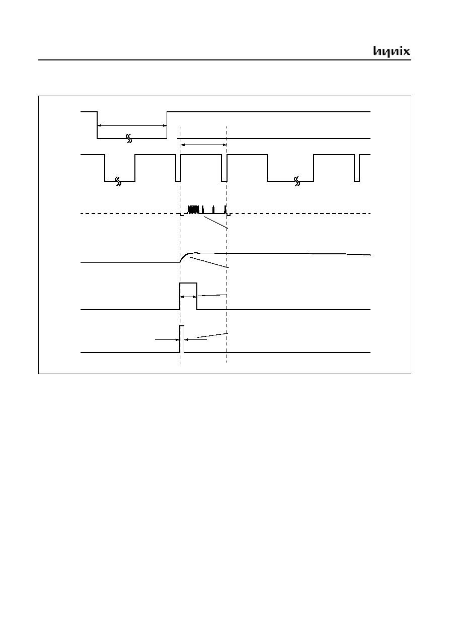
HMS81C4x60
84
November 2001 Ver 1.1
Figure 18-11 Signal timing
[Example]
Initializing slicer register.
CCD_INIT: LDM
SLINF0,#0011_0011b
; slicer line 21
LDM
SLINF1,#0000_0000b
; no field
LDM
RIKST,#01
; run-in key start : 1 -> 0.125uS(8MHz)
LDM
RIKED,#8Ch
; run-in key end : 8ch -> 17.5uS(8MHz)
LDM
SNCST,#01
; sync tip start : 1 -> 0.0625uS(16MHz)
LDM
SNCED,#58h
; sync tip end : 58h -> 5.5uS(16MHz)
LDM
SLCON,#01h
; normal clock, 16MHz, slicer start
Vsync
Hsync
CVBS
SCAP
RIK
Sync_tip
5V
5V
5V
5V
2.5V
2V
2.2V
0V
0V
5V
5V
0.5V
2
3
4
1
1 Hsync cycle
Run-in key start/stop timming
Sync-tip start/stop timming
Slicer capacitor charging level
line 21 signal
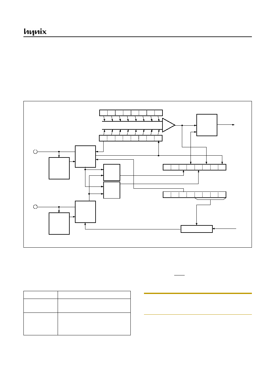
HMS81C4x60
November 2001 Ver 1.1
85
19. I
2
C Bus Interface
The I
2
C Bus interface circuit is shown in Figure 19-1.
The multi-master I
2
C Bus interface is a serial communica-
tions circuit, conforming to the Phlips I
2
C Bus data trans-
fer format. This interface, offering both arbitration lost
detection and a synchronous functions, is useful for the
multi-master serial communications.
This multi-master I
2
C Bus interface circuit consists of the
I
2
C address register, the I
2
C data shift register, the I
2
C
clock control register, the I
2
C control register, the I
2
C sta-
tus register and other control circuits.
The more details about registers are shown Figure 19-2~
Figure 19-5.
Figure 19-1 Block Diagram of multi-master I
2
C circuit
Control
The HMS81C4x60 contains two I
2
C Bus interface mod-
ules. It supports multi-master function, so it contains arbi-
tration lost detection, synchronization function,etc.
I
2
C address register
It contains slave address (7bit) which is used during slave
mode and Read/Write bit.
Bit 7 ~ 1 : Slave address 6~0
Note: Bit 7~1 (SAD6~0) store slave address. The address
data transmitted from the master is compared with the con-
tents of these bits.
ICAR [D8
H
]
IFI2CR
SCL
Address
comparator
ICDR [D9
H
]
D7
D6
D5
D4
D3
D2
D1
D0
Interrupt
Generation
Circuit
Data
Control
Circuit
ICSR [00DA
H
]
MST
TRX
BB
PIN
AL
AD0
ADRb
LRB
Noise
Elimination
Circuit
AL
Circuit
BB
Circuit
Clock
Control
Circuit
Noise
Elimination
Circuit
ICCR [00DB
H
]
B SEL1
CCR3
ESO
Clock division
Clock Source
SDA
SAD6 SDA5 SDA4 SDA3 SDA2 SDA1 SDA0 RWb
B SEL1 ACKb
CCR2 CCR1 CCR0
ITEM
Function
Format
Philips
I
2
C
standard
7bit addressing format
Communication
mode
Master transmitter
Master receiver
Slave transmitter
Slave receiver
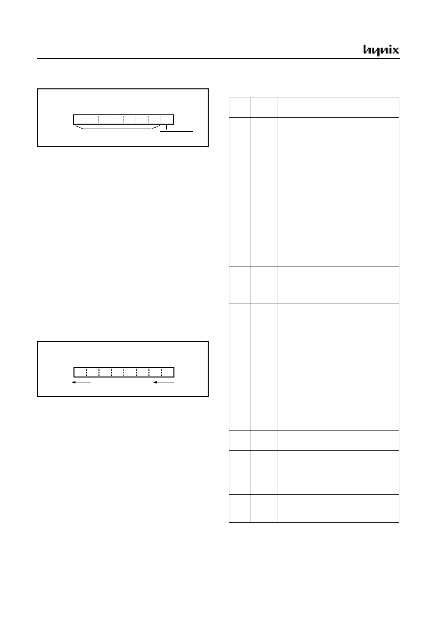
HMS81C4x60
86
November 2001 Ver 1.1
Figure 19-2 I
2
C address Register
I
2
C data shift register [ICDR]
The I
2
C data shift register is an 8bit shift register to store
received data and write transmit data.
When transmit data is written into this register, it is trans-
fered to the outside from bit7 in synchronization with the
SCL clock, and each time one-bit data is output, the data of
this register are shifted one bit to the left. When data is re-
ceived, it is input to this register from bit0 in synchroniza-
tion with the SCL clock, and each time one-bit data is
input, the data of this register are shifted one bit to the left.
The I
2
C data shift register is in a write enable status only
when the ESO bit of the I
2
C control register (address
00DC
H
) is "1". The bit counter is reset by a write instruc-
tion to the I
2
C data shift register. Reading data from the
I
2
C data shift register is always enabled regardless of the
ESO bit value.
Figure 19-3 Data shift register
I
2
C status register
The I
2
C status register controls the I
2
C Bus interface sta-
tus. The low-order 4bits are read only bits and the high-or-
der 4bits can be read out and written to.
The more details about its bits are shown Table 19-1.
ICAR
ADDRESS : 00D8
H
RESET VALUE : 0000 0000
b
SAD6 SDA5 SDA4 SDA3 SDA2 SDA1 SDA0 RWb
Slave address
RW
RW
RW
RW
RW
RW
RW
R
Read/Write Bit
ICDR
ADDRESS : 00D9
H
RESET VALUE : 0000 0000
b
RW
RW
RW
RW
RW
RW
RW
RW
D7
D6
D5
D4
D3
D2
D1
D0
S hift left 1-bit ea ch S C L
Bit
No.
Name
Function
7
6
MST
TRX
00: Slave / Receiver mode
01: Slave / Transmitter mode
10: Master / Receiver mode
11: Master / Transmitter mode
MST is cleared when
- After reset.
- After the arbitration lost is occured and
1 byte data transmission is finished.
- After stop condition is detected.
- When start condition is disabled by
start condition duplication preventation
function.
TRX is cleared when
- After reset.
- When arbitration lost or stop condition
is occured .
- When MST is `0', and start condition
or ACK non-return mode is detected.
5
BB
BB(Bus busy)bit is 1 during bus is busy.
This bit can be written by S/W. its value
is `1' by start condition, and cleared by
stop condition.
4
PIN
PIN(Pending Interrupt Not)bit is inter-
rupt request bit.
If I
2
C interrupt request is issued, its
value is 0.
PIN is cleared when
- After 1 byte trasmission / receive is fin-
ished.
PIN is set when
- After reset.
- After write instruction is excuted into
I
2
C data shift register ICDR.
- When PIN bit low, the output of SCL is
pulled down, So if you want to release
SCL, you must perform write instruction
CDR.
3
AL
Arbitration lost detection flag.
If arbitration lost is detected, AL=1, or 0.
2
AD0
General call detection flag.
If general call is detected, AD0=1, or
not 0.
* General call : If received address is all
`0' . it is called general call.
1
ADRb
Address represent flag
0 : current contents is address
1 : current contents is data

HMS81C4x60
November 2001 Ver 1.1
87
Figure 19-4 I
2
C status Register
I
2
C control register
It controls communication data format.
It controls SCL mode, SCL frequency, etc.
It contains 8bit data to transmit to external device when tr-
asmitter mode, or received 8bit data from external device
when receive mode.
Figure 19-5 I
2
C control Register
Figure 19-6 Interrupt request signal generation timing
0
LRB
Last received bit.
it is used for receive confirmation. If
ACK is returned, LRB=0, or not 1.
Bit
No.
Name
Function
Table 19-1 Bit function
ICSR
ADDRESS : 00DA
H
RESET VALUE : 0001 0000
b
RW
RW
RW
RW
R
R
R
R
MST
TRX
BB
PIN
AL
AD0
ADRb
LRB
ICCR
ADDRESS : 00DB
H
RESET VALUE : 0000 0000
b
ESO
CCR3 CCR2 CCR1 CCR0
BSEL0
RW
RW
RW
RW
RW
RW
RW
BSEL1
ACKb
RW
SCL
PIN
I
2
C Request
Bit
No.
Name
Function
7
6
BSEL1
BSEL0
I
2
C connection control.
00: No connection
01: SCL0, SDA0
10: SCL1, SDA1
11: SCL0, SDA0, SCL1, SDA1
5
ACK
If acknowlege clock is returned, this bit
is 0, or not 1.
4
ESO
I
2
C Bus interface use enable flag
0: Disabled
1: Enabled
3
2
1
0
CCR3
CCR2
CCR1
CCR0
SCL Frequency selection
SCL frequency = f
ex
/ (12 * CCR)
Value
f
ex
= 4MHz
0000
0001
0010
0011
0100
0101
0110
0111
1000
1001
1010
1011
1100
1101
1110
1111
Not allowed
Not allowed
333.3KHz
222.2KHz
166.6KHz
133.3KHz
111.1KHz
95.2KHz
83.3KHz
74.1KHz
66.6KHz
60.6KHz
55.5KHz
51.3KHz
47.6KHz
44.4KHz
Table 19-2 Bit function
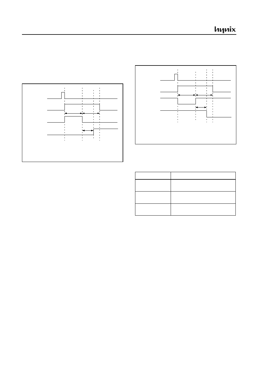
HMS81C4x60
88
November 2001 Ver 1.1
START condition generation
When the ESO bit of the I
2
C control register (00DB
H
) is
"1", writing to the I
2
C status register will generate START
condition. Refer to Figure 19-7 for the START condition
generation timing diagram.
Figure 19-7 START condition generation timing
RESTART condition generation
RESTART condition's setting sequence is as followings.
1. Write 020
H
to I
2
C status register (ICSR, 00DA
H
)
2. Write slave address to I
2
C data shift register (ICDR,
00D9
H
)
3. Write 0F0
H
to I
2
C status register (ICSR, 00DA
H
)
STOP condition generation
Writing `C0h' to ICSR will generate a stop condition,
when ESO (ICCR bit3) is `1'
Figure 19-8 STOP condition generating timing diagram
START / STOP condition generation time is shown Table
19-3.
ICSR write signal
SCL
SDA
BB (Bus busy) flag
t
SETUP
t
HOLD
t
BB
: Setup time
: Hold time
: Set time for BB
t
SETUP
t
HOLD
t
BB
(I
2
C status reg.)
ITEM
Timing SPEC.
Setup time
( t
SETUP
)
3.3uS (n=20cycles)
Hold time
( t
HOLD
)
3.3uS (n=20cycles)
Set/Reset time for
BB flag ( t
BB
)
3.0uS (n=18cycles)
Table 19-3 Example time ( f
ex
=4MHz )
ICSR write signal
SCL
SDA
BB (Bus busy) flag
t
SETUP
t
HOLD
t
BB
: Setup time
: Hold time
: Set time for BB
t
SETUP
t
HOLD
t
BB
(I
2
C status reg.)

HMS81C4x60
November 2001 Ver 1.1
89
START / STOP condition detect
START / STOP condition is detected when Table 19-3 is
satisfied.
Figure 19-9 START / STOP condition detection timing
START / STOP detection time is showed Table 19-4.
Address data communication
The first transmitted data from master is compared with
I
2
C address register (ICAR, 00D8
H
). At this time R/W is
not compared but it determines next data operation. i.e,
transmitting or receiving data
Figure 19-10 Address data communication format
SCL
SDA (START)
SDA (STOP)
t
SETUP
t
HOLD
: Setup time
: Hold time
t
SETUP
t
HOLD
SCL release time
ITEM
Timing SPEC.
SCL release time
> 2.0uS (n=12cycles)
Setup time
> 1.0uS (n=6cycles)
Hold time
> 1.0uS (n=6cycles)
Table 19-4 Example time ( f
ex
=4MHz )
Master -> Slave (with 7bit address)
START
R/W
ACK
ACK
ACK
/ACK
Data
STOP
Slave addr.
Slave -> Master (with 7bit address)
Data block from master to slave
Data block from slave to master
7bit
Data
START
R/W
ACK
ACK
ACK
Data
STOP
Slave addr.
7bit
Data
("1")
("0")
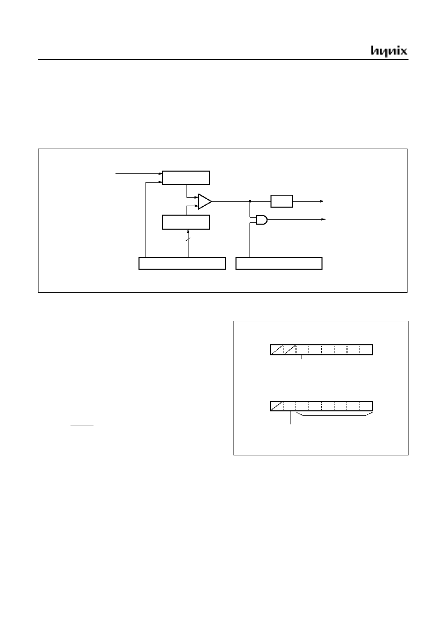
HMS81C4x60
90
November 2001 Ver 1.1
20. WATCHDOG TIMER
The watchdog timer rapidly detects the CPU malfunction
such as endless looping caused by noise or the like, and re-
sumes the CPU to the normal state.
The watchdog timer signal for detecting malfunction can
be selected either a reset CPU or a interrupt request.
When the watchdog timer is not being used for malfunc-
tion detection, it can be used as a timer to generate an in-
terrupt at fixed intervals.
Figure 20-1 Block Diagram of Watchdog Timer
Watchdog Timer Control
Figure 20-2 shows the watchdog timer control register.
The watchdog timer is automatically disabled after reset.
The CPU malfunction is detected as setting the detection
time, selecting output, and clearing the binary counter. Re-
peatedly clearing the binary counter within the setting de-
tection time.
If the malfunction occurs for any cause, the watchdog tim-
er output will become active at the rising overflow from
the binary counters unless the binary counter are cleared.
At this time, when WDTON=1 a reset is generated, which
drives the RESET pin low to reset the internal hardware.
When WDTON=0, a watchdog timer interrupt (IFWDT) is
generated.
Figure 20-2 Watchdog timer register
to reset CPU
WDTR
Watchdog Timer Register
(BIT overflow : IFBIT)
Clock source
6-bit up-counter
enable
WDT
6-bit compare data
comparator
6
WDTR[bit5~0]
Watchdog Timer interrupt
WDTCL[bit6]
clear
[00D7
H
]
IFWDT
CKCTLR
Clock control Register
[00D6
H
]
WDTON[bit5]
CKCTLR
ADDRESS : 00D6
H
RESET VALUE : 0000 0000
b
WDT
ENP BTCL BTS2 BTS1 BTS0
Watchdog timer On/Off control
W
W
W
W
W
R
WDTR
ADDRESS : 00D7
H
RESET VALUE : -011 1111
b
WDT
W D T R 5 ~ 0
Slave address
W
W
W
W
W
W
W
ON
CK
0: Normal 6bit timer, Watchdog off
1: Watchdog timer
CL
Watchdog timer Clear
0: Watchdog timer free run
1: Watchdog timer clear and free run
Automatically cleared this bit after 1cycle
HMS81C4x60
November 2001 Ver 1.1
91
Example: Sets the watchdog timer detection time
Enable and Disable Watchdog
Watchdog timer is enabled by setting WDTON (bit 5 in
CKTCLR) to "1". WDTON is initialized to "0" during re-
set, WDTON should be set to "1" to operate after reset is
released.
Example: Enables watchdog timer reset
:
LDM
CKTCLR,#001?????b ;WDTON
1
:
:
The watchdog timer is disabled by clearing bit 5 (WD-
TON) of CKTCLR.
Watchdog Timer Interrupt
The watchdog timer can also be used as a simple 6-bit tim-
er by clearing bit 5 (WDTON) of CKTCLR. The interval
of watchdog timer interrupt is decided by Basic Interval
Timer.
Interval equation is shown as below.
The stack pointer (SP) should be initialized before using
the watchdog timer output as an interrupt source.
Example: 6-bit timer interrupt setting up.
LDX
#03FH
TXSP
;SP
3F
LDM
CKTCLR,#000?????b ;WDTON
0
LDM
WDTR,#01??????b ;WDTCL
0
:
:
Refer table and see BIT timer ().
LDM
WDTR,#01??????b
;
Clear Counter and set value(??????b)
;
You have to set WDTR first, for prevent unpredictable interrupt
;
when you set WDTON bit.
LDM
CKCTLR,#00111???b
;
Select clock source(???b)
and WDTON=1
LDM
WDTR,#01??????b
;
Clear counter
:
:
:
:
LDM
WDTR,#01??????b
;
Clear counter
:
:
:
:
LDM
WDTR,#01??????b
;
Clear counter
Within WDT
detection time
Within WDT
detection time
T
WDTR
Interval of BIT
◊
=
CKCTLR
BTS2~0
BIT input
clock
Watchdog
timer input
clock
IFWDT cycle
000
b
PS4 (4uS)
1,024uS
32,256uS
001
b
PS5 (8uS)
2,028uS
64,512uS
010
b
PS6 (16uS)
4,096uS
129,024uS
011
b
PS7 (32uS)
8,192uS
258,048uS
100
b
PS8 (64uS)
16,384uS
516,096uS
101
b
PS9 (128uS)
32,768uS
1,032,192uS
110
b
PS10 (256uS)
65,536uS
2,064,384uS
111
b
PS11 (512uS)
131,072uS
4,128,768uS
Table 20-1 Watchdog timer MAX. cycle (Ex:f
ex
=4MHz)
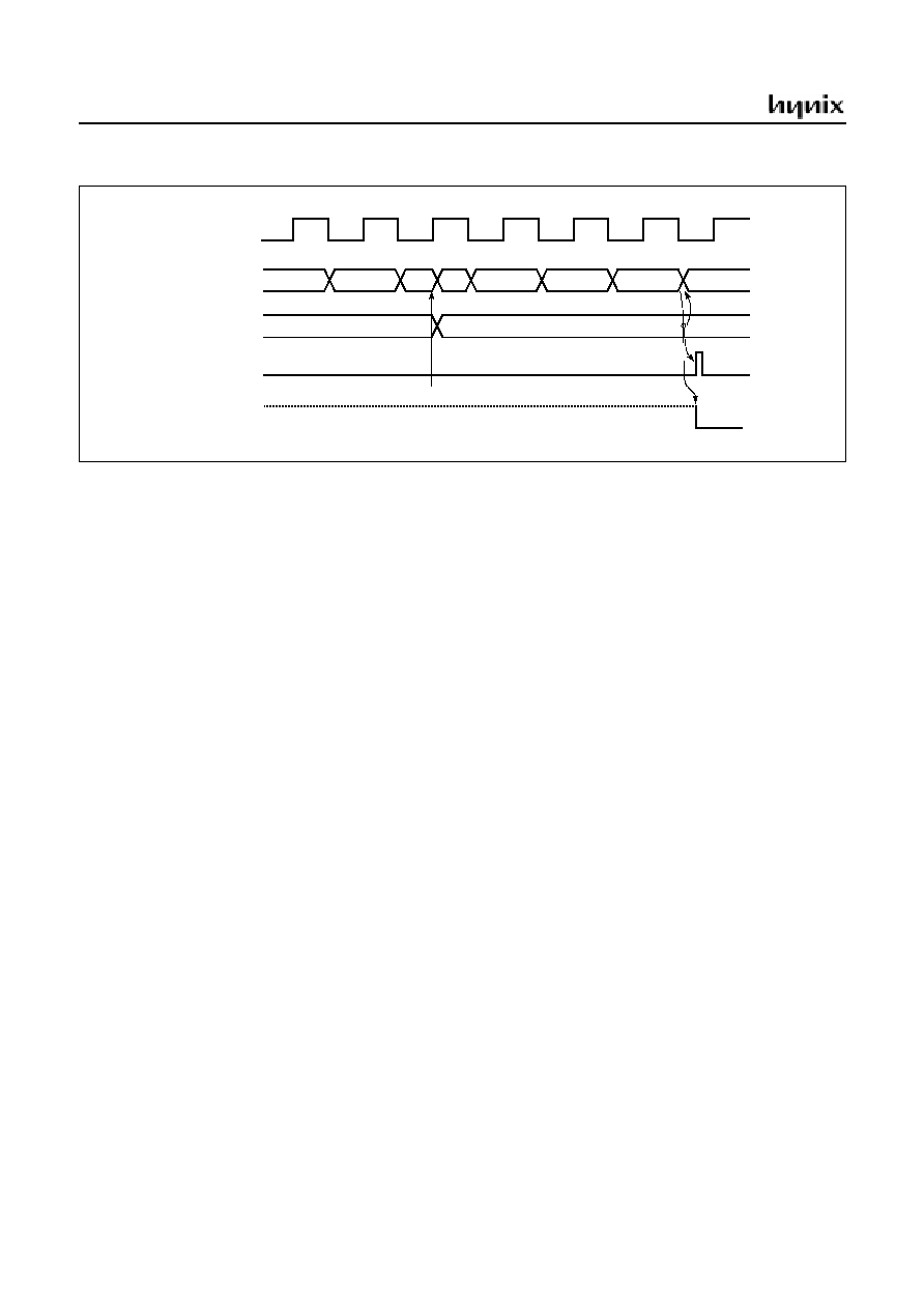
HMS81C4x60
92
November 2001 Ver 1.1
Figure 20-3 Watchdog timer Timing
Minimizing Current Consumption
It should be set properly that current flow through port
doesn't exist.
First conseider the setting to input mode. Be sure that there
is no current flow after considering its relationship with
external circuit. In input mode, the pin impedance viewing
from external MCU is very high that the current doesn't
flow.
But input voltage level should be V
SS
or V
DD
. Be careful
that if unspecified voltage, i.e. if unfirmed voltage level is
applied to input pin, there can be little current (max. 1mA
at around 2V) flow.
If it is not appropriate to set as an input mode, then set to
output mode considering there is no current flow. Setting
to High or Low is decided considering its relationship with
external circuit. For example, if there is external pull-up re-
sistor then it is set to output mode, i.e. to High, and if there
is external pull-down register, it is set to low. See Figure
20-4.
2
3
n
Source clock
Binary-counter
WDTR
IFWDT interrupt
WDTR
"0100_0011b"
1
0
Match
Detect
Counter
Clear
1
2
3
0
BIT overflow
3
WDT reset
reset
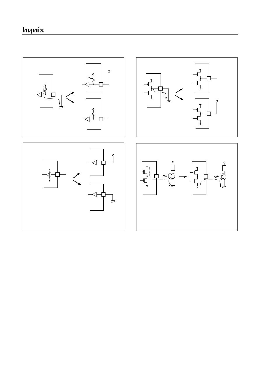
HMS81C4x60
November 2001 Ver 1.1
93
Figure 20-4 Application example of Port under Power Consumption
INPUT PIN
V
DD
GND
i
V
DD
OUTPUT PIN
GND
i
X
Weak pull-up current flows
In the left case, much current flows from port to GND.
X
ON
OFF
V
DD
internal
pull-up
OUTPUT PIN
GND
i
In the left case, Tr. base current flows from port to GND.
i=0
X
OFF
ON
V
DD
L
ON
OFF
OPEN
GND
V
DD
L
ON
OFF
To avoid power consumption, low output to the port .
INPUT PIN
i
V
DD
X
Very weak current flows
V
DD
O
O
OPEN
ON
OFF
OPEN
i=0
O
O
V
DD
O
i=0
O
GND
O
When port is configured as an input, input level should
be closed to 0V or 5V to avoid power consumption.
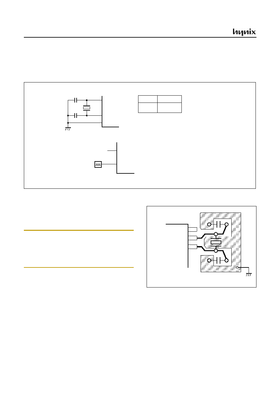
HMS81C4x60
94
November 2001 Ver 1.1
21. OSCILLATOR CIRCUIT
The HMS81C4x60 has two oscillation circuits internally.
X
IN
and X
OUT
are input and output for main frequency and
OSC1 and OSC2 are input and output for OSD(On Screen
display) frequency, respectively, of a inverting amplifier
which can be configured for use as an on-chip oscillator, as
shown in Figure 21-1 .
Figure 21-1 Oscillation Circuit
Oscillation components have their own characteristics, so
user should consult the component manufacturers for ap-
propriate values of external components.
In addition, see Figure 21-2 for the layout of the crystal.
Note: Minimize the wiring length. Do not allow wiring to in-
tersect with other signal conductors. Do not allow wiring to
come near changing high current. Set the potential of the
grounding position of the oscillator capacitor to that of V
SS
.
Do not ground to any ground pattern where high current is
present. Do not fetch signals from the oscillator.
Figure 21-2 Layout example of Oscillator PCB circuit
X
OUT
X
IN
V
SS
Recommend
C1
C2
X
OUT
X
IN
External Clock
Open
External Oscillator
Crystal Oscillator
fc (MHz)
fc (MHz)
4
C1 & C2 (pF)
15
X
OUT
X
IN
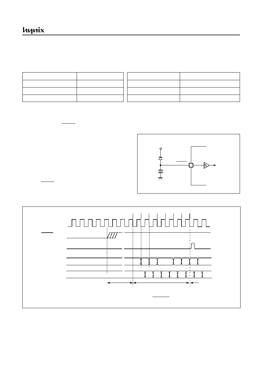
HMS81C4x60
November 2001 Ver 1.1
95
22. RESET
The HMS81C4x60 have two types of reset generation pro-
cedures; one is an external reset input, other is a watch-dog
timer reset. Table 22-1 shows on-chip hardware initializa-
tion by reset action.
Table 22-1 Initializing Internal Status by Reset Action
22.1 External Reset Input
The reset input is the RESET pin, which is the input to a
Schmitt Trigger. A reset in accomplished by holding the
RESET pin low for at least 8 oscillator periods, within the
operating voltage range and oscillation stable, a reset is ap-
plied and the internal state is initialized. After reset, 64ms
(at 4 MHz) add with 7 oscillator periods are required to
start execution as shown in Figure 22-2 .
Internal RAM is not affected by reset. When V
DD
is turned
on, the RAM content is indeterminate. Therefore, this
RAM should be initialized before reading or testing it.
When the RESET pin input goes high, the reset operation
is released and the program execution starts at the vector
address stored at addresses FFFE
H
- FFFF
H
.
A connecting for simple power-on-reset is shown in Figure
22-1 .
Figure 22-1 Simple Power-on-Reset Circuit
Figure 22-2 Timing Diagram after RESET
On-chip Hardware
Initial Value
On-chip Hardware
Initial Value
Program counter
PC
(FFFF
H
) - (FFFE
H
)
Peripheral clock
Off
RAM page register
DPGR
00
H
Watchdog timer
Disable
G-flag of PSW
G
0
Control registers
Refer to Table 8-1 on page 22
RESET
+
-
V
DD
GND
MCU
MAIN PROGRAM
Oscillator
(X
IN
pin)
?
?
FFFE FFFF
Stabilization Time
t
ST
= 62.5mS at 4.19MHz
RESET
ADDRESS
DATA
1
2
3
4
5
6
7
?
?
Start
?
?
?
FE
?
ADL
ADH
OP
BUS
BUS
RESET Process Step
~~
~~
~~
~~
~~
~~
t
ST
=
x 256
f
MAIN
˜
1024
1
Fetch
~~

HMS81C4x60
96
November 2001 Ver 1.1
22.2 Watchdog Timer Reset
Refer to "20. WATCHDOG TIMER" on page 90.

HMS81C4x60
November 2001 Ver 1.1
97
23. OTP Programming
23.1 HMS87C4x60 OTP Programming
User can burn out HMS87C4x60 OTP through the general
Gang programmer using special ROM writer. In Devleop-
ment tool package auxiliary, HMS87C4x60 has ROM
writer socket. HMS87C4x60 have two ROM memory ar-
eas. One is Program ROM memory and the other is Font
ROM memory. Program ROM area is from 1000h to
FFFFh Font ROM area is from 10000h to 17FFFh.
Blank Check
Figure 23-1 HMS87C4x60 OTP Memory Map
Program Writing
There are two kind of OTP file. One is program OTP
file(***.OTP) and the other is font OTP file(***.FNT).
You can make each file through ASMLINKER.exe and
OSDFONT.exe respectively. All OTP file is Motolora S-
format. You can burn the program file and font file respec-
tively or together. To burn program file and font file re-
spectively, refer following procedure
1. Make program OTP file and font OTP file repec-
tively.
2. Burn program OTP file(Set chip target address
1000h ~ FFFFh)
3. Burn font OTP file(Set chip target address 10000h
~17FFFh)
To burn program file and font file together, refer following
procedure
1. Add program OTP file and font OTP file
2. Burn OTP file(Set chip target address 1000h ~
17FFFh)
About other details, refer ROM wirter manual.
1000H
FFFFH
17FFFH
OSD Font
Memory
Program
Memory
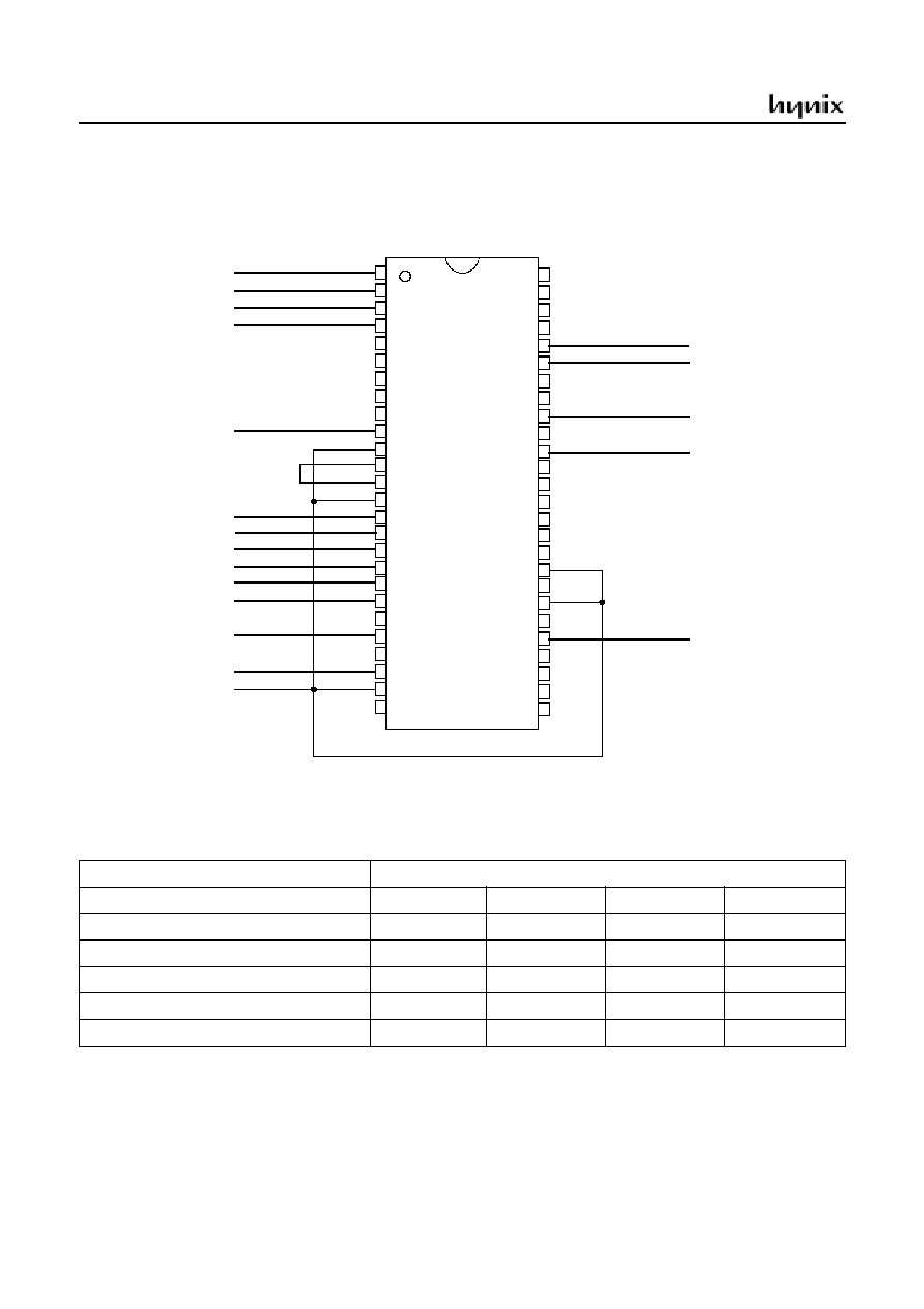
HMS81C4x60
98
November 2001 Ver 1.1
23.2 .Device Configuration Data
Figure 23-2 Figure Pin Configuration in OTP Programming Mode
Figure 23-3 Figure Mode Table
HYNIX
HMS87C
426
0
OM1
OM2
OM3
PGMB
DIO<4>
DIO<2>
DIO<3>
OEB
CEB
AHB
ALB
32SDIP
DIO<1>
DIO<0>
DIO<6>
DIO<5>
VPP
A16
1
2
3
4
5
6
7
8
9
10
11
12
13
14
15
16
17
18
19
20
21
22
23
24
25
26
52
51
50
49
48
47
46
45
44
43
42
41
40
39
38
37
36
35
34
33
32
31
30
29
28
27
DIO<7>
HMS87C4x60
Mode
VPP
CEB
OEB
PGMB
Program
11.25
Low
High
Low
Verify
11.25
Low
Low
High
Optional Verify
5
Low
Low
X
Gang Write
11.25
Low
High
Low
Gang Verify
11.25, 5
Low
Low
X

HMS81C4x60
November 2001 Ver 1.1
99
24. Assemble mnemonics
24.1 Instruction Map
00000
00
00001
01
00010
02
00011
03
00100
04
00101
05
00110
06
00111
07
01000
08
01001
09
01010
0A
01011
0B
01100
0C
01101
0D
01110
0E
01111
0F
000
NOP
SET1
dp.bit
BBS
A.bit,rel
BBS
dp.bit,rel
ADC
#imm
ADC
dp
ADC
dp+X
ADC
!abs
ASL
A
ASL
dp
TCALL
0
SETA1
.bit
BIT
dp
POP
A
PUSH
A
BRK
001
CLRC
//
//
//
SBC
#imm
SBC
dp
SBC
dp+X
SBC
!abs
ROL
A
ROL
dp
TCALL
2
CLRA1
.bit
COM
dp
POP
X
PUSH
X
BRA
rel
010
CLRG
//
//
//
CMP
#imm
CMP
dp
CMP
dp+X
CMP
!abs
LSR
A
LSR
dp
TCALL
4
NOT1
M.bit
TST
dp
POP
Y
PUSH
Y
PCALL
Upage
011
DI
//
//
//
OR
#imm
OR
dp
OR
dp+X
OR
!abs
ROR
A
ROR
dp
TCALL
6
OR1
OR1B
CMPX
dp
POP
PSW
PUSH
PSW
RET
100
CLRV
//
//
//
AND
#imm
AND
dp
AND
dp+X
AND
!abs
INC
A
INC
dp
TCALL
8
AND1
AND1B
CMPY
dp
CBNE
dp+X
TXSP
INC
X
101
SETC
//
//
//
EOR
#imm
EOR
dp
EOR
dp+X
EOR
!abs
DEC
A
DEC
dp
TCALL
10
EOR1
EOR1B
DBNE
dp
XMA
dp+X
TSPX
DEC
X
110
SETG
//
//
//
LDA
#imm
LDA
dp
LDA
dp+X
LDA
!abs
TXA
LDY
dp
TCALL
12
LDC
LDCB
LDX
dp
LDX
dp+Y
XCN
DAS
111
EI
//
//
//
LDM
dp,#imm
STA
dp
STA
dp+X
STA
!abs
TAX
STY
dp
TCALL
14
STC
M.bit
STX
dp
STX
dp+Y
XAS
10000
10
10001
11
10010
12
10011
13
10100
14
10101
15
10110
16
10111
17
11000
18
11001
19
11010
1A
11011
1B
11100
1C
11101
1D
11110
1E
11111
1F
000
BPL
rel
CLR1
dp.bit
BBC
A.bit,rel
BBC
dp.bit,rel
ADC
{X}
ADC
!abs+Y
ADC
[dp+X]
ADC
[dp]+Y
ASL
!abs
ASL
dp+X
TCALL
1
JMP
!abs
BIT
!abs
ADDW
dp
LDX
#imm
JMP
[!abs]
001
BVC
rel
//
//
//
SBC
{X}
SBC
!abs+Y
SBC
[dp+X]
SBC
[dp]+Y
ROL
!abs
ROL
dp+X
TCALL
3
CALL
!abs
TEST
!abs
SUBW
dp
LDY
#imm
JMP
[dp]
010
BCC
rel
//
//
//
CMP
{X}
CMP
!abs+Y
CMP
[dp+X]
CMP
[dp]+Y
LSR
!abs
LSR
dp+X
TCALL
5
MUL
TCLR1
!abs
CMPW
dp
CMPX
#imm
CALL
[dp]
011
BNE
rel
//
//
//
OR
{X}
OR
!abs+Y
OR
[dp+X]
OR
[dp]+Y
ROR
!abs
ROR
dp+X
TCALL
7
DBNE
Y
CMPX
!abs
LDYA
dp
CMPY
#imm
RETI
100
BMI
rel
//
//
//
AND
{X}
AND
!abs+Y
AND
[dp+X]
AND
[dp]+Y
INC
!abs
INC
dp+X
TCALL
9
DIV
CMPY
!abs
INCW
dp
INC
Y
TAY
101
BVS
rel
//
//
//
EOR
{X}
EOR
!abs+Y
EOR
[dp+X]
EOR
[dp]+Y
DEC
!abs
DEC
dp+X
TCALL
11
XMA
{X}
XMA
dp
DECW
dp
DEC
Y
TYA
110
BCS
rel
//
//
//
LDA
{X}
LDA
!abs+Y
LDA
[dp+X]
LDA
[dp]+Y
LDY
!abs
LDY
dp+X
TCALL
13
LDA
{X}+
LDX
!abs
STYA
dp
XAY
DAA
111
BEQ
rel
//
//
//
STA
{X}
STA
!abs+Y
STA
[dp+X]
STA
[dp]+Y
STY
!abs
STY
dp+X
TCALL
15
STA
{X}+
STX
!abs
CBNE
dp
XYX
NOP

HMS81C4x60
100
November 2001 Ver 1.1
24.2 Alphabetic order table of instruction
NO.
MNENONIC
OP
CODE
BYTE
NO.
CYCLE
NO
OPERATION
FLAG
NVGBHIZC
1
ADC #imm
04
2
2
Add with carry.
NV - - H - ZC
2
ADC dp
05
2
3
A
A + (M) + C
3
ADC dp + X
06
2
4
4
ADC !abs
07
3
4
5
ADC !abs+Y
15
3
5
6
ADC [dp+X]
16
2
6
7
ADC [dp]+Y
17
2
6
8
ADC {X}
14
1
3
9
ADDW dp
1D
2
5
16-bits add without carry : YA
YA + (dp+1)(dp)
NV - - H - ZC
10
AND #imm
84
2
2
Logical AND
N - - - - - Z -
11
AND dp
85
2
3
A
A ^ (M)
12
AND dp + X
86
2
4
13
AND !abs
87
3
4
14
AND !abs+Y
95
3
5
15
AND [dp+X]
96
2
6
16
AND [dp] + Y
97
2
6
17
AND {X}
94
1
3
18
AND1 M.bit
8B
3
4
Bit AND C-flag : C
C ^ (M.bit)
- - - - - - - C
19
AND1B M.bit
8B
3
4
Bit AND C-flag and NOT : C
C ^ ~(M.bit)
- - - - - - - C
20
ASL A
08
1
2
Arithmetic shift left
N - - - - - ZC
21
ASL dp
09
2
4
22
ASL dp + X
19
2
5
23
ASL !abs
18
3
5
24
BBC A.bit,rel
y2
2
4/6
Branch if bit clear :
- - - - - - - -
25
BBC dp.bit,rel
y3
3
5/7
if(bit) = 0, then PC
PC + rel
26
BBS A.bit,rel
x2
2
4/6
Branch if bit clear :
- - - - - - - -
27
BBS dp.bit,rel
x3
3
5/7
if(bit) = 1, then PC
PC + rel
28
BCC rel
50
2
2/4
Branch if carry bit clear :
if(C) = 0, then PC
PC + rel
MM - - - - Z -
29
BCS rel
D0
2
2/4
Branch if carry bit set : If (C) =1, then PC
PC + rel
- - - - - - - -
30
BEQ rel
F0
2
2/4
Branch if equal : if (Z) = 1, then PC
PC + rel
- - - - - - - -
31
BIT dp
0C
2
4
Bit test A with memory :
MM - - - - Z -
32
BIT !abs
1C
3
5
Z
A ^ M, N
(M
7
), V
(M
6
)
33
BMI rel
90
2
2/4
Branch if munus : if (N) = 1, then PC
PC + rel
- - - - - - - -
34
BNE rel
70
2
2/4
Branch if not equal : if (Z) = 0, then PC
PC + rel
- - - - - - - -
35
BPL rel
10
2
2/4
Branch if not minus : if (N) = 0, then PC
PC + rel
- - - - - - - -
36
BRA rel
2F
2
4
Branch always : PC
PC + rel
- - - - - - - -
37
BRK
0F
1
8
Software interrupt:
- - - 1 - 0 - -
B
"1", M(SP)
(PC
H
), SP
SP - 1,
M(s)
(PC
L
), SP
S - 1, M(SP)
PSW,
SP
SP - 1, PC
L
(0FFDE
H
), PC
H
(0FFDF
H
)
38
BVC rel
30
2
2/4
Branch if overflow bit clear :
- - - - - - - -
If (V) = 0, then PC
PC + rel
39
BVS rel
B0
2
2/4
Branch if overflow bit set :
- - - - - - - -
If (V) = 1, then PC
PC + rel
40
CALL !abs
3B
3
8
Subroutine call
- - - - - - - -
41
CALL [dp]
5F
2
8
M(SP)
(PC
H
), SP
SP-1, M(SP)
(PC
L
), SP
SP-1
if !abs, PC
abs ; if [dp], PC
L
(dp), PC
H
(dp+1)
42
CBNE dp,rel
FD
3
5/7
Compare and branch if not equal ;
- - - - - - - -
43
CBNE dp + X, rel
8D
3
6/8
If A
(M), then PC
PC + rel.
44
CLR1 dp.bit
y1
2
4
Clear bit : (M.bit)
"0"
- - - - - - - -
45
CLR1A A.bit
2B
2
2
Clear A.bit : (A.bit)
"0"
- - - - - - - -
46
CLRC
20
1
2
Clear C-flag : C
"0"
- - - - - - - 0
47
CLRG
40
1
2
Clear G-flag : G
"0"
- - 0 - - - - -
C 7 6 5 4 3 2 1 0
"
0
"

HMS81C4x60
November 2001 Ver 1.1
101
48
CLRV
80
1
2
Clear V-flag : V
"0"
- 0 - - 0 - - -
49
CMP #imm
44
2
2
Compare accumulator contents with memory contents
N - - - - - ZC
50
CMP dp
45
2
3
A - (M)
51
CMP dp + X
46
2
4
52
CMP !abs
47
3
4
53
CMP !abs + Y
55
3
5
54
CMP [dp + X]
56
2
6
55
CMP [dp] + Y
57
2
6
56
CMP {X}
54
1
3
57
CMPW dp
5D
2
4
Compare YA contents with memory pair contents :
N - - - - - ZC
YA - (dp+1)(dp)
58
CMPX #imm
5E
2
2
Compare X contents with memory contents
N - - - - - ZC
59
CMPX dp
6C
2
3
X - (M)
60
CMPX !abs
7C
3
4
61
CMPY #imm
7E
2
2
Compare Y contents with memory contents
N - - - - - ZC
62
CMPY dp
8C
2
3
Y - (M)
63
CMPY !abs
9C
3
4
64
COM dp
2C
2
4
1's complement : (dp)
~(dp)
N - - - - - Z -
65
DAA
DF
1
3
Decimal adjust for addition
N - - - - - ZC
66
DAS
CF
1
3
Decimal adjust for substraction
N - - - - - ZC
67
DBNE dp,rel
AC
3
5/7
Decrement and branch if not equal :
- - - - - - - -
68
DBNE Y,rel
7B
2
4/6
if (M)
0, then PC
PC + rel.
69
DEC A
A8
1
2
Decrement
N - - - - - Z -
70
DEC dp
A9
2
4
M
M - 1
71
DEC dp + X
B9
2
5
72
DEC !abs
B8
3
5
73
DEC X
AF
1
2
74
DEC Y
BE
1
2
75
DECW dp
BD
2
6
Decrement memory pair : (dp+1)(dp)
{(dp+1)(dp)} - 1
N - - - - - Z -
76
DI
60
1
3
Disable interrupts : I
"0"
- - - - - 0 - -
77
DIV
9B
1
12
Divide : YA / X
Q:A, R:Y
NV - - H - Z -
78
EI
E0
1
3
Enable interrupts : I
"1"
- - - - - 1 - -
79
EOR #imm
A4
2
2
Exclusive OR
N - - - - - Z -
80
EOR dp
A5
2
3
A
A
(M)
81
EOR dp + X
A6
2
4
82
EOR !abs
A7
3
4
83
EOR !abs + Y
B5
3
5
84
EOR [ dp + X]
96
2
6
85
EOR [dp] + Y
97
2
6
86
EOR {X}
94
1
3
87
EOR1 M.bit
AB
3
5
Bit exclusive-OR C-flag : C
C
(M.bit)
- - - - - - - C
88
EOR1B M.bit
AB
3
5
Bit exclusive-OR C-flag and NOT : C
C
(M.bit)
- - - - - - - C
89
INC A
88
1
2
Increment
N - - - - - ZC
90
INC dp
89
2
4
(M)
(M) + 1
N - - - - - Z -
91
INC dp + X
99
2
5
92
INC !abs
98
3
5
93
INC X
8F
1
2
94
INC Y
9E
1
2
95
INCW dp
9D
2
6
Increment memory pair : (dp+1)(dp)
{(dp+1)(dp)} + 1
N - - - - - Z -
96
JMP !abs
1B
3
3
Unconditional jump
- - - - - - - -
97
JMP [!abs]
1F
3
5
PC
jump address
98
JMP [dp]
3F
2
4
NO.
MNENONIC
OP
CODE
BYTE
NO.
CYCLE
NO
OPERATION
FLAG
NVGBHIZC
HMS81C4x60
102
November 2001 Ver 1.1
99
LDA #imm
C4
2
2
Load accumulator
N - - - - - Z -
100
LDA dp
C5
2
3
A
(M)
101
LDA dp + X
C6
2
4
102
LDA !abs
C7
3
4
103
LDA !abs + Y
D5
3
5
104
LDA [dp + X]
D6
2
6
105
LDA [dp]+Y
D7
2
6
106
LDA {X}
D4
1
3
107
LDA {X}+
DB
1
4
X-register auto-increment : A
(M), X
X + 1
108
LDC M.bit
CB
3
4
Load C-flag : C
(M.bit)
- - - - - - - C
109
LDCB M.bit
CB
3
4
Load C-flag with NOT : C
~(M.bit)
- - - - - - - C
110
LDM dp,#imm
E4
3
5
Load memory with immediate data : (M)
imm
- - - - - - - -
111
LDX #imm
1E
2
2
Load X-register
N - - - - - Z -
112
LDX dp
CC
2
3
X
(M)
113
LDX dp + Y
CD
2
4
114
LDX !abs
DC
3
4
115
LDY #imm
3E
2
2
Load X-register
N - - - - - Z -
116
LDY dp
C9
2
3
Y
(M)
117
LDY dp + Y
D9
2
4
118
LDY !abs
D8
3
4
119
LDYA dp
7D
2
5
Load YA : YA
(dp+1)(dp)
N - - - - - Z -
120
LSR A
48
1
2
Logical shift right
N - - - - - ZC
121
LSR dp
49
2
4
122
LSR dp + X
59
2
5
123
LSR !abs
58
3
5
124
MUL
5B
1
9
Multiply : YA
Y x A
N - - - - - Z -
125
NOP
00,FF
1
2
No operation
- - - - - - - -
126
NOT1 M.bit
4B
3
5
Bit complement : (M.bit)
~(M.bit)
- - - - - - - -
127
OR #imm
64
2
2
Logical OR
N - - - - - Z -
128
OR dp
65
2
3
A
A V (M)
129
OR dp + X
66
2
4
130
OR !abs
67
3
4
131
OR !abs + Y
75
3
5
132
OR [dp +X}
76
2
6
133
OR [dp] + Y
77
2
6
134
OR {X}
74
1
3
135
OR1 M.bit
6B
3
5
Bit OR C-flag : C
C V (M.bit)
- - - - - - - C
136
OR1B M.bit
6B
3
5
Bit OR C-flag and NOT : C
C V ~(M.bit)
- - - - - - - C
137
PCALL
4F
2
6
U-page call : M(SP)
(PC
H
), SP
SP -1,
- - - - - - - -
M(SP)
(PC
L
), SP
SP -1,
PC
L
(upage), PC
H
"OFF
H
"
138
POP A
0D
1
4
Pop from stack
- - - - - - - -
139
POP X
2D
1
4
SP
SP + 1, Reg.
M(SP)
140
POP Y
4D
1
4
141
POP PSW
6D
1
4
(restored)
142
PUSH A
0E
1
4
Push to stack
- - - - - - - -
143
PUSH X
2E
1
4
M(SP)
Reg. SP
SP - 1
144
PUSH Y
4E
1
4
145
PUSH PSW
6E
1
4
146
RET
6F
1
5
Return from subroutine :
- - - - - - - -
SP
SP+1, PC
L
M(SP), SP
SP+1, PC
H
M(SP)
147
RETI
7F
1
6
Return from interrupt :
(restored)
SP
SP+1, PSW
M(SP), SP
SP+1,PC
L
M(SP),
SP
SP+1, PC
H
M(SP)
NO.
MNENONIC
OP
CODE
BYTE
NO.
CYCLE
NO
OPERATION
FLAG
NVGBHIZC
7 6 5 4 3 2 1 0 C
"
0
"
HMS81C4x60
November 2001 Ver 1.1
103
148
ROL A
28
1
2
Rotate left through carry
N - - - - - ZC
149
ROL dp
29
2
4
150
ROL dp + X
39
2
5
151
ROL !abs
38
3
5
152
ROR A
68
1
2
Rotate right through carry
N - - - - - ZC
153
ROR dp
69
2
4
154
ROR dp + X
79
2
5
155
ROR !abs
78
3
5
156
SBC #imm
24
2
2
Substract with carry
NV - - HZC
157
SBC dp
25
2
3
A
A - (M) - ~(C)
158
SBC dp + X
26
2
4
159
SBC !abs
27
3
4
160
SBC !abs + Y
35
3
5
161
SBC [dp + X]
36
2
6
162
SBC [dp] + Y
37
2
6
163
SBC {X}
34
1
3
164
SET1 dp.bit
x1
2
4
Set bit : (M.bit)
"1"
- - - - - - - -
165
SETA1 A.bit
0B
2
2
Set A.bit : (A.bit)
"1"
- - - - - - - -
166
SETC
A0
1
2
Set C-flag : C
"1"
- - - - - - - 1
167
SETG
C0
1
2
Set G-flag : G
"1"
- - 1 - - - - -
168
STA dp
E5
2
3
Store accumulator contents in memory
- - - - - - - -
169
STA dp + X
E6
2
4
(M)
A
170
STA !abs
E7
3
4
171
STA !abs + Y
F5
3
5
172
STA [dp + X]
F6
2
6
173
STA [dp] + Y
F7
2
6
174
STA {X}
F4
1
3
175
STA {X}+
FB
1
4
X-register auto-increment : (M)
A, X
X + 1
176
STC M.bit
EB
3
6
Store C-flag : (M.bit)
C
- - - - - - - -
177
STX dp
EC
2
4
Store X-register contents in memory
- - - - - - - -
178
STX dp + Y
ED
2
5
(M)
X
179
STX !abs
FC
3
5
180
STY dp
E9
2
4
Store Y-register contents in memory
- - - - - - - -
181
STY dp + X
F9
2
5
(M)
Y
182
STY !abs
F8
3
5
183
STYA dp
DD
2
5
Store YA : (dp+1)(dp)
YA
- - - - - - - -
184
SUBW dp
3D
2
5
16-bits substract without carry : YA
YA - (dp+1)(dp)
NV - - H - ZC
185
TAX
E8
1
2
Transfer accumulator contents to X-register : X
A
N - - - - - Z -
186
TAY
9F
1
2
Transfer accumulator contents to Y-register : Y
A
N - - - - - Z -
187
TCALL n
nA
1
8
Table call :
- - - - - - - -
M(SP)
(PC
H
), SP
SP -1,
M(SP)
(PC
L
), SP
SP -1
PC
L
(Table vector L), PC
H
(Table vector H)
188
TCLR1 !abs
5C
3
6
Test and clear bits with A :
N - - - - - Z -
A - (M), (M)
(M) ^ ~(A)
189
TSET1 !abs
3C
3
6
Test and set bits with A :
N - - - - - Z -
A - (M), (M)
(M) V (A)
190
TSPX
AE
1
2
Transfer stack-pointer contents to X-register : X
SP
N - - - - - Z -
191
TST dp
4C
2
3
Test memory contents for negative or zero : (dp) - 00
H
N - - - - - Z -
192
TXA
C8
1
2
Transfer X-register contents to accumulator : A
X
N - - - - - Z -
193
TXSP
8E
1
2
Transfer X-register contents to stack-pointer : SP
X
N - - - - - Z -
194
TYA
BF
1
2
Transfer Y-register contents to accumulator : A
Y
N - - - - - Z -
195
XAX
EE
1
4
Exchange X-register contents with accumulator : X
f
A
- - - - - - - -
196
XAY
DE
1
4
Exchange Y-register contents with accumulator : Y
f
A
- - - - - - - -
NO.
MNENONIC
OP
CODE
BYTE
NO.
CYCLE
NO
OPERATION
FLAG
NVGBHIZC
C 7 6 5 4 3 2 1 0
7 6 5 4 3 2 1 0 C
HMS81C4x60
104
November 2001 Ver 1.1
24.3 Instruction Table by Function
1. Arithmetic/Logic Operation
197
XCN
CE
1
5
Exchange nibbles within the accumulator:
N - - - - - Z -
A
7
~ A
4
f
A
3
~ A
0
198
XMA dp
BC
2
5
Exchange memory contents with accumulator
N - - - - - Z -
199
XMA dp + X
AD
2
6
(M)
f
A
200
XMA {X}
BB
1
5
201
XYX
FE
1
4
Exchange X-register contents with Y-register : X
f
Y
- - - - - - - -
NO.
MNENONIC
OP
CODE
BYTE
NO.
CYCLE
NO
OPERATION
FLAG
NVGBHIZC
NO.
MNENONIC
OP
CODE
BYTE
NO.
CYCLE
NO
OPERATION
FLAG
NVGBHIZC
1
ADC #imm
04
2
2
Add with carry.
NV - - H - ZC
2
ADC dp
05
2
3
A
A + (M) + C
3
ADC dp + X
06
2
4
4
ADC !abs
07
3
4
5
ADC !abs+Y
15
3
5
6
ADC [dp+X]
16
2
6
7
ADC [dp]+Y
17
2
6
8
ADC {X}
14
1
3
9
AND #imm
84
2
2
Logical AND
N - - - - - Z -
10
AND dp
85
2
3
A
A ^ (M)
11
AND dp + X
86
2
4
12
AND !abs
87
3
4
13
AND !abs+Y
95
3
5
14
AND [dp+X]
96
2
6
15
AND [dp] + Y
97
2
6
16
AND {X}
94
1
3
17
ASL A
08
1
2
Arithmetic shift left
N - - - - - ZC
18
ASL dp
09
2
4
19
ASL dp + X
19
2
5
20
ASL !abs
18
3
5
21
CMP #imm
44
2
2
Compare accumulator contents with memory contents
N - - - - - ZC
22
CMP dp
45
2
3
A - (M)
23
CMP dp + X
46
2
4
24
CMP !abs
47
3
4
25
CMP !abs + Y
55
3
5
26
CMP [dp + X]
56
2
6
27
CMP [dp] + Y
57
2
6
28
CMP {X}
54
1
3
29
CMPX #imm
5E
2
2
Compare X contents with memory contents
N - - - - - ZC
30
CMPX dp
6C
2
3
X - (M)
31
CMPX !abs
7C
3
4
32
CMPY #imm
7E
2
2
Compare Y contents with memory contents
N - - - - - ZC
33
CMPY dp
8C
2
3
Y - (M)
34
CMPY !abs
9C
3
4
35
COM dp
2C
2
4
1's complement : (dp)
~(dp)
N - - - - - Z -
36
DAA
DF
1
3
Decimal adjust for addition
N - - - - - ZC
37
DAS
CF
1
3
Decimal adjust for substraction
N - - - - - ZC
38
DEC A
A8
1
2
Decrement
N - - - - - Z -
39
DEC dp
A9
2
4
M
M - 1
40
DEC dp + X
B9
2
5
41
DEC !abs
B8
3
5
42
DEC X
AF
1
2
43
DEC Y
BE
1
2
C 7 6 5 4 3 2 1 0
"
0
"

HMS81C4x60
November 2001 Ver 1.1
105
44
DIV
9B
1
12
Divide : YA /
X
Q:A, R:Y
NV - - H - Z -
45
EOR #imm
A4
2
2
Exclusive OR
N - - - - - Z -
46
EOR dp
A5
2
3
A
A
(M)
47
EOR dp + X
A6
2
4
48
EOR !abs
A7
3
4
49
EOR !abs + Y
B5
3
5
50
EOR [ dp + X]
96
2
6
51
EOR [dp] + Y
97
2
6
52
EOR {X}
94
1
3
53
INC A
88
1
2
Increment
N - - - - - ZC
54
INC dp
89
2
4
(M)
(M) + 1
N - - - - - Z -
55
INC dp + X
99
2
5
56
INC !abs
98
3
5
57
INC X
8F
1
2
58
INC Y
9E
1
2
59
LSR A
48
1
2
Logical shift right
N - - - - - ZC
60
LSR dp
49
2
4
61
LSR dp + X
59
2
5
62
LSR !abs
58
3
5
63
MUL
5B
1
9
Multiply : YA
Y x A
N - - - - - Z -
64
OR #imm
64
2
2
Logical OR
N - - - - - Z -
65
OR dp
65
2
3
A
A V (M)
66
OR dp + X
66
2
4
67
OR !abs
67
3
4
68
OR !abs + Y
75
3
5
69
OR [dp +X}
76
2
6
70
OR [dp] + Y
77
2
6
71
OR {X}
74
1
3
72
ROL A
28
1
2
Rotate left through carry
N - - - - - ZC
73
ROL dp
29
2
4
74
ROL dp + X
39
2
5
75
ROL !abs
38
3
5
76
ROR A
68
1
2
Rotate right through carry
N - - - - - ZC
77
ROR dp
69
2
4
78
ROR dp + X
79
2
5
79
ROR !abs
78
3
5
80
SBC #imm
24
2
2
Substract with carry
NV - - HZC
81
SBC dp
25
2
3
A
A - (M) - ~(C)
82
SBC dp + X
26
2
4
83
SBC !abs
27
3
4
84
SBC !abs + Y
35
3
5
85
SBC [dp + X]
36
2
6
86
SBC [dp] + Y
37
2
6
87
SBC {X}
34
1
3
88
TST dp
4C
2
3
Test memory contents for negative or zero : (dp) - 00
H
N - - - - - Z -
89
XCN
CE
1
5
Exchange nibbles within the accumulator:
N - - - - - Z -
A
7
~ A
4
f
A
3
~ A
0
NO.
MNENONIC
OP
CODE
BYTE
NO.
CYCLE
NO
OPERATION
FLAG
NVGBHIZC
7 6 5 4 3 2 1 0 C
"
0
"
C 7 6 5 4 3 2 1 0
7 6 5 4 3 2 1 0 C
HMS81C4x60
106
November 2001 Ver 1.1
2. Register / Memory Operation
3. 16-Bit Operation
NO.
MNENONIC
OP
CODE
BYTE
NO.
CYCLE
NO
OPERATION
FLAG
NVGBHIZC
1
LDA #imm
C4
2
2
Load accumulator
N - - - - - Z -
2
LDA dp
C5
2
3
A
(M)
3
LDA dp + X
C6
2
4
4
LDA !abs
C7
3
4
5
LDA !abs + Y
D5
3
5
6
LDA [dp + X]
D6
2
6
7
LDA [dp]+Y
D7
2
6
8
LDA {X}
D4
1
3
9
LDA {X}+
DB
1
4
X-register auto-increment : A
(M), X
X + 1
10
LDM dp,#imm
E4
3
5
Load memory with immediate data : (M)
imm
- - - - - - - -
11
LDX #imm
1E
2
2
Load X-register
N - - - - - Z -
12
LDX dp
CC
2
3
X
(M)
13
LDX dp + Y
CD
2
4
14
LDX !abs
DC
3
4
15
LDY #imm
3E
2
2
Load X-register
N - - - - - Z -
16
LDY dp
C9
2
3
Y
(M)
17
LDY dp + Y
D9
2
4
18
LDY !abs
D8
3
4
19
STA dp
E5
2
3
Store accumulator contents in memory
- - - - - - - -
20
STA dp + X
E6
2
4
(M)
A
21
STA !abs
E7
3
4
22
STA !abs + Y
F5
3
5
23
STA [dp + X]
F6
2
6
24
STA [dp] + Y
F7
2
6
25
STA {X}
F4
1
3
26
STA {X}+
FB
1
4
X-register auto-increment : (M)
A, X
X + 1
27
STX dp
EC
2
4
Store X-register contents in memory
- - - - - - - -
28
STX dp + Y
ED
2
5
(M)
X
29
STX !abs
FC
3
5
30
STY dp
E9
2
4
Store Y-register contents in memory
- - - - - - - -
31
STY dp + X
F9
2
5
(M)
Y
32
STY !abs
F8
3
5
33
TAX
E8
1
2
Transfer accumulator contents to X-register : X
A
N - - - - - Z -
34
TAY
9F
1
2
Transfer accumulator contents to Y-register : Y
A
N - - - - - Z -
35
TSPX
AE
1
2
Transfer stack-pointer contents to X-register : X
SP
N - - - - - Z -
36
TXA
C8
1
2
Transfer X-register contents to accumulator : A
X
N - - - - - Z -
37
TXSP
8E
1
2
Transfer X-register contents to stack-pointer : SP
X
N - - - - - Z -
38
TYA
BF
1
2
Transfer Y-register contents to accumulator : A
Y
N - - - - - Z -
39
XAX
EE
1
4
Exchange X-register contents with accumulator : X
f
A
- - - - - - - -
40
XAY
DE
1
4
Exchange Y-register contents with accumulator : Y
f
A
- - - - - - - -
41
XMA dp
BC
2
5
Exchange memory contents with accumulator
N - - - - - Z -
42
XMA dp + X
AD
2
6
(M)
f
A
43
XMA {X}
BB
1
5
44
XYX
FE
1
4
Exchange X-register contents with Y-register : X
f
Y
- - - - - - - -
NO.
MNENONIC
OP
CODE
BYTE
NO.
CYCLE
NO
OPERATION
FLAG
NVGBHIZC
1
ADDW dp
1D
2
5
16-bits add without carry : YA
YA + (dp+1)(dp)
NV - - H - ZC
2
CMPW dp
5D
2
4
Compare YA contents with memory pair contents :
N - - - - - ZC
YA - (dp+1)(dp)
3
DECW dp
BD
2
6
Decrement memory pair : (dp+1)(dp)
{(dp+1)(dp)} - 1
N - - - - - Z -
4
INCW dp
9D
2
6
Increment memory pair : (dp+1)(dp)
{(dp+1)(dp)} + 1
N - - - - - Z -

HMS81C4x60
November 2001 Ver 1.1
107
4. Bit Manipulation
5. Branch / Jump Operation
5
LDYA dp
7D
2
5
Load YA : YA
(dp+1)(dp)
N - - - - - Z -
6
STYA dp
DD
2
5
Store YA : (dp+1)(dp)
YA
- - - - - - - -
7
SUBW dp
3D
2
5
16-bits substract without carry : YA
YA - (dp+1)(dp)
NV - - H - ZC
NO.
MNENONIC
OP
CODE
BYTE
NO.
CYCLE
NO
OPERATION
FLAG
NVGBHIZC
NO.
MNENONIC
OP
CODE
BYTE
NO.
CYCLE
NO
OPERATION
FLAG
NVGBHIZC
1
AND1 M.bit
8B
3
4
Bit AND C-flag : C
C ^ (M.bit)
- - - - - - - C
2
AND1B M.bit
8B
3
4
Bit AND C-flag and NOT : C
C ^ ~(M.bit)
- - - - - - - C
3
BIT dp
0C
2
4
Bit test A with memory :
MM - - - - Z -
4
BIT !abs
1C
3
5
Z
A ^ M, N
(M
7
), V
(M
6
)
5
CLR1 dp.bit
y1
2
4
Clear bit : (M.bit)
"0"
- - - - - - - -
6
CLR1A A.bit
2B
2
2
Clear A.bit : (A.bit)
"0"
- - - - - - - -
7
CLRC
20
1
2
Clear C-flag : C
"0"
- - - - - - - 0
8
CLRG
40
1
2
Clear G-flag : G
"0"
- - 0 - - - - -
9
CLRV
80
1
2
Clear V-flag : V
"0"
- 0 - - 0 - - -
10
EOR1 M.bit
AB
3
5
Bit exclusive-OR C-flag : C
C
(M.bit)
- - - - - - - C
11
EOR1B M.bit
AB
3
5
Bit exclusive-OR C-flag and NOT : C
C
(M.bit)
- - - - - - - C
12
LDC M.bit
CB
3
4
Load C-flag : C
(M.bit)
- - - - - - - C
13
LDCB M.bit
CB
3
4
Load C-flag with NOT : C
~(M.bit)
- - - - - - - C
14
NOT1 M.bit
4B
3
5
Bit complement : (M.bit)
~(M.bit)
- - - - - - - -
15
OR1 M.bit
6B
3
5
Bit OR C-flag : C
C V (M.bit)
- - - - - - - C
16
OR1B M.bit
6B
3
5
Bit OR C-flag and NOT : C
C V ~(M.bit)
- - - - - - - C
17
SET1 dp.bit
x1
2
4
Set bit : (M.bit)
"1"
- - - - - - - -
18
SETA1 A.bit
0B
2
2
Set A.bit : (A.bit)
"1"
- - - - - - - -
19
SETC
A0
1
2
Set C-flag : C
"1"
- - - - - - - 1
20
SETG
C0
1
2
Set G-flag : G
"1"
- - 1 - - - - -
21
STC M.bit
EB
3
6
Store C-flag : (M.bit)
C
- - - - - - - -
22
TCLR1 !abs
5C
3
6
Test and clear bits with A :
N - - - - - Z -
A - (M), (M)
(M) ^ ~(A)
23
TSET1 !abs
3C
3
6
Test and set bits with A :
N - - - - - Z -
A - (M), (M)
(M) V (A)
NO.
MNENONIC
OP
CODE
BYTE
NO.
CYCLE
NO
OPERATION
FLAG
NVGBHIZC
1
BBC A.bit,rel
y2
2
4/6
Branch if bit clear :
- - - - - - - -
2
BBC dp.bit,rel
y3
3
5/7
if(bit) = 0, then PC
PC + rel
3
BBS A.bit,rel
x2
2
4/6
Branch if bit clear :
- - - - - - - -
4
BBS dp.bit,rel
x3
3
5/7
if(bit) = 1, then PC
PC + rel
5
BCC rel
50
2
2/4
Branch if carry bit clear :
if(C) = 0, then PC
PC + rel
MM - - - - Z -
6
BCS rel
D0
2
2/4
Branch if carry bit set : If (C) =1, then PC
PC + rel
- - - - - - - -
7
BEQ rel
F0
2
2/4
Branch if equal : if (Z) = 1, then PC
PC + rel
- - - - - - - -
8
BMI rel
90
2
2/4
Branch if munus : if (N) = 1, then PC
PC + rel
- - - - - - - -
9
BNE rel
70
2
2/4
Branch if not equal : if (Z) = 0, then PC
PC + rel
- - - - - - - -
10
BPL rel
10
2
2/4
Branch if not minus : if (N) = 0, then PC
PC + rel
- - - - - - - -
11
BRA rel
2F
2
4
Branch always : PC
PC + rel
- - - - - - - -
12
BVC rel
30
2
2/4
Branch if overflow bit clear :
- - - - - - - -
If (V) = 0, then PC
PC + rel
13
BVS rel
B0
2
2/4
Branch if overflow bit set :
- - - - - - - -
If (V) = 1, then PC
PC + rel

HMS81C4x60
108
November 2001 Ver 1.1
6. Control Operation & etc.
14
CALL !abs
3B
3
8
Subroutine call
- - - - - - - -
15
CALL [dp]
5F
2
8
M(SP)
(PC
H
), SP
SP-1, M(SP)
(PC
L
), SP
SP-1
if !abs, PC
abs ; if [dp], PC
L
(dp), PC
H
(dp+1)
16
CBNE dp,rel
FD
3
5/7
Compare and branch if not equal ;
- - - - - - - -
17
CBNE dp + X, rel
8D
3
6/8
If A
(M), then PC
PC + rel.
18
DBNE dp,rel
AC
3
5/7
Decrement and branch if not equal :
- - - - - - - -
19
DBNE Y,rel
7B
2
4/6
if (M)
0, then PC
PC + rel.
20
JMP !abs
1B
3
3
Unconditional jump
- - - - - - - -
21
JMP [!abs]
1F
3
5
PC
jump address
22
JMP [dp]
3F
2
4
23
PCALL
4F
2
6
U-page call : M(SP)
(PC
H
), SP
SP -1,
- - - - - - - -
M(SP)
(PC
L
), SP
SP -1,
PC
L
(upage), PC
H
"OFF
H
"
24
TCALL n
nA
1
8
Table call :
- - - - - - - -
M(SP)
(PC
H
), SP
SP -1,
M(SP)
(PC
L
), SP
SP -1
PC
L
(Table vector L), PC
H
(Table vector H)
NO.
MNENONIC
OP
CODE
BYTE
NO.
CYCLE
NO
OPERATION
FLAG
NVGBHIZC
NO.
MNENONIC
OP
CODE
BYTE
NO.
CYCLE
NO
OPERATION
FLAG
NVGBHIZC
1
BRK
0F
1
8
Software interrupt:
- - - 1 - 0 - -
B
"1", M(SP)
(PC
H
), SP
SP - 1,
M(s)
(PC
L
), SP
S - 1, M(SP)
PSW,
SP
SP - 1, PC
L
(0FFDE
H
), PC
H
(0FFDF
H
)
2
DI
60
1
3
Disable interrupts : I
"0"
- - - - - 0 - -
3
EI
E0
1
3
Enable interrupts : I
"1"
- - - - - 1 - -
4
NOP
FF
1
2
No operation
- - - - - - - -
5
POP A
0D
1
4
Pop from stack
- - - - - - - -
6
POP X
2D
1
4
SP
SP + 1, Reg.
M(SP)
7
POP Y
4D
1
4
8
POP PSW
6D
1
4
(restored)
9
PUSH A
0E
1
4
Push to stack
- - - - - - - -
10
PUSH X
2E
1
4
M(SP)
Reg. SP
SP - 1
11
PUSH Y
4E
1
4
12
PUSH PSW
6E
1
4
13
RET
6F
1
5
Return from subroutine :
- - - - - - - -
SP
SP+1, PC
L
M(SP), SP
SP+1, PC
H
M(SP)
14
RETI
7F
1
6
Return from interrupt :
(restored)
SP
SP+1, PSW
M(SP), SP
SP+1,PC
L
M(SP),
SP
SP+1, PC
H
M(SP)