HMS87C5216
Sep. 2001 Ver 1.0
1
HMS87C5216
CMOS SINGLE-CHIP 8-BIT MICROCONTROLLER
FOR UR(Universal Remocon) & WIRELESS KEYBOARD
1. OVERVIEW
1.1 Description
The HMS87C5216 is an advanced CMOS 8-bit microcontroller with 16K bytes of ROM. The device is one of GMS800 fam-
ily. The HYNIX Semicon HMS87C5216 is a powerful microcontroller which provides a highly flexible and cost effective
solution to many UR & Keyboard applications. The HMS87C5216 provides the following standard features: 16K bytes of
ROM, 320 bytes of RAM, 8-bit timer/counter, on-chip oscillator,clock circuitry and RC wake up function. 4 chanel ADC, In
addition, the HMS87C5216 Series supports power saving modes to reduce power consumption
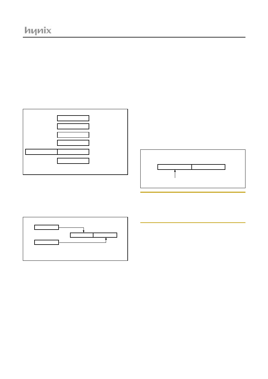
1.2 Features
∑ Instruction Cycle Time:
- 1us at 4MHz
∑ Programmable I/O pins
∑ Operating Voltage
- 2.0 ~ 5.5 V @ 4MHz
∑ Timer
- Timer / Counter ......... 16Bit * 1ch
........ 16Bit * 2ch
- Basic Interval Timer ...... 8Bit * 1ch
- Watch Dog Timer ............ 6Bit * 1ch
∑ 8 Interrupt sources
* Nested Interrupt control is available.
- External input: 2
- Keyscan input
- Basic Interval Timer
- Watchdog timer
- Timer : 3
∑ Power On Reset
∑ Power saving Operation Modes
- STOP
- SLEEP
∑ Low Voltage Detection Circuit
∑ Watch Dog Timer Auto Start (During 1second
after Power on Reset)
∑ 4 CHANEL ADC
∑ RC TIMER WAKE UP
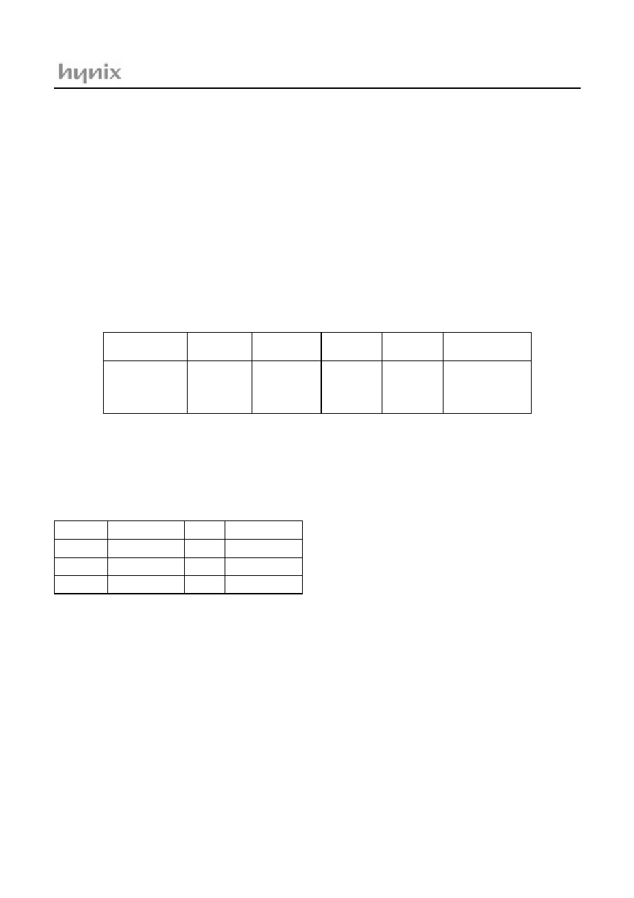
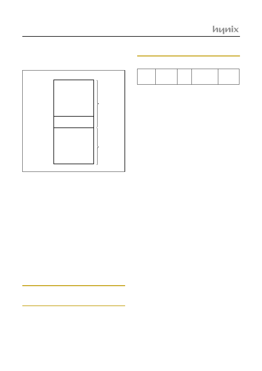
Device name
ROM Size
EPROM Size
RAM Size
Operatind
Voltage
Package
HMS87C5216
-
16K byte
320bytes
2.0 ~ 5.5V
28 SOP
40 PDIP
44 PLCC
44 QFP
28 PIN
40 PIN
44 PIN
INPUT
2
2
2
OUTPUT
2
2
2
I/O
22
34
38

HMS87C5216
2
Sep. 2001 Ver 1.0
1.3 Development Tools
The
HMS87C5216
and
HMS87C5216
are supported by a
full-featured macro assembler, an in-circuit emulator
CHOICE-Dr
TM
.
In Circuit Emulators
CHOICE-Dr.
Assembler
HME Macro Assembler
OTP Writer
Single Writer : Sigma
4-Gang Writer : Dr.Gang
OTP Devices
HMS87C5216
HMS87C5216
Sep. 2001 Ver 1.0
3
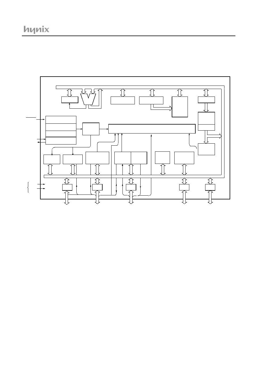
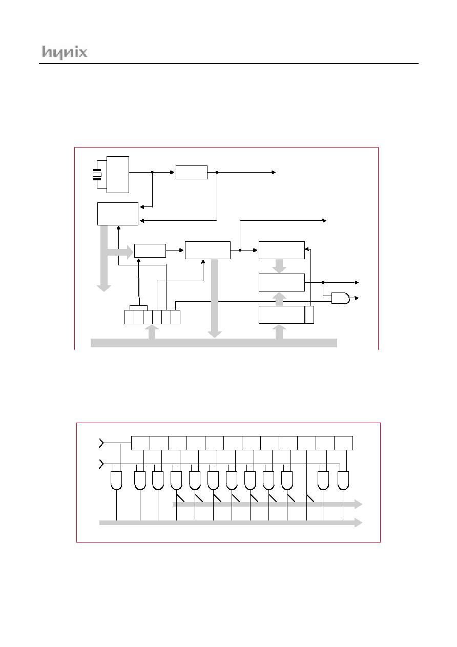
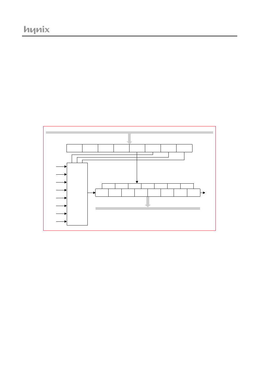
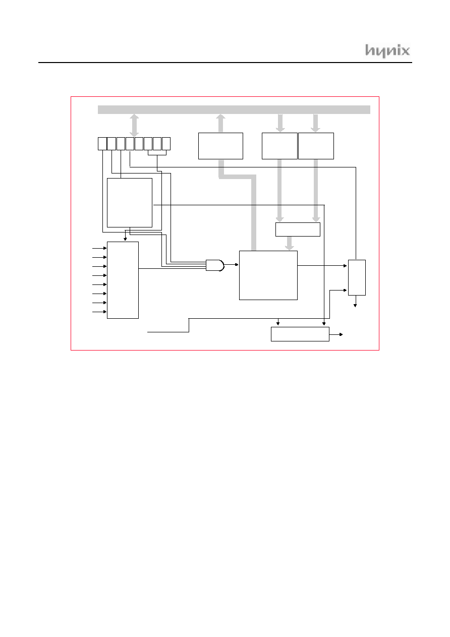
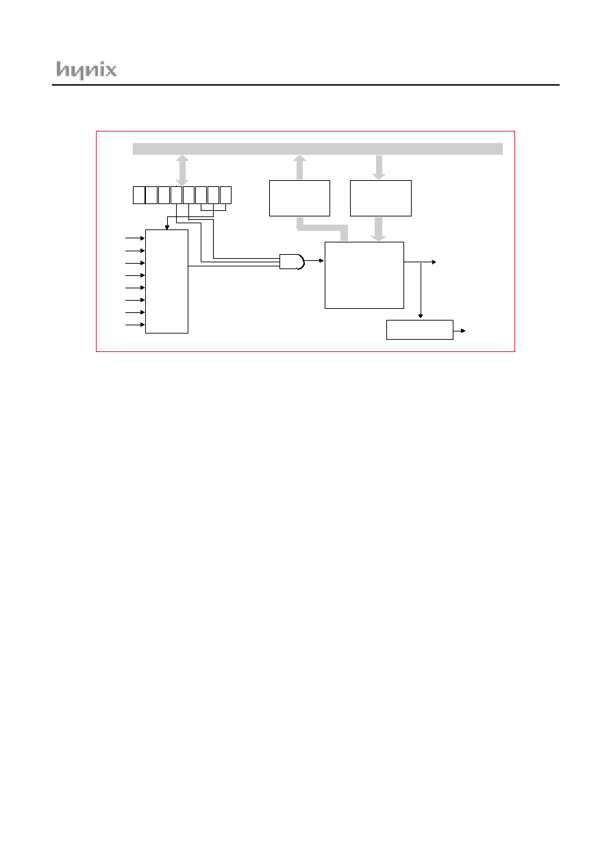
2. BLOCK DIAGRAM
ALU
Accumulator
Stack Pointer
Inte rrupt C ontroller
Data
Memory
8-bit
Converter
A/D
8-bit
Counter
Timer/
Program
Memory
Data Table
PC
8-bit Basic
Timer
Interval
Watch-dog
Instruction
R1
R2
R3
RC Watch
Timer
PSW
System controller
Timing generator
System
Clock Controller
Clock Generator
RESET
Xin
Xout
R10 / INT1
R11 / INT2
R12 / T0
R13 / T1
R14 / AN0
R15 / AN1
R16 / AN2
R17 / AN3
R20
R21
R22
R23
R24 /T2
V
DD
V
SS
Power
Supply
Decoder
Carrier
R25 / EC0
R26
R27
R4
LVD/POR
R0
R00 / KS0
R01 / KS1
R02 / KS2
R03 / KS3
R04 / KS4
R05 / KS5
R06 / KS6
R07 / KS7
Key Wake up
Generator
REMOUT
R30
R31
R32
R33
R34
R35
R36
R37
R40
R41
R42
R43
R44
HMS87C5216
4
Sep. 2001 Ver 1.0
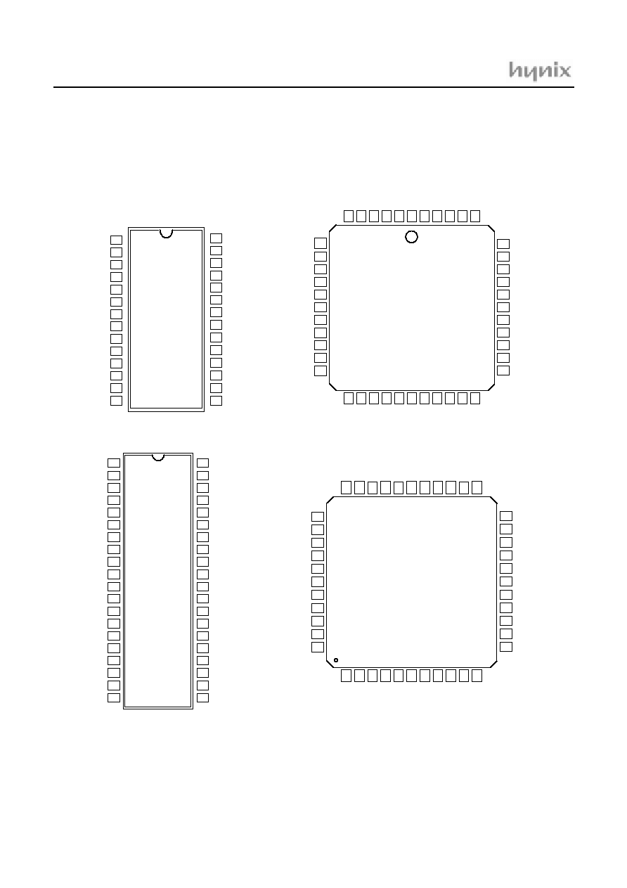
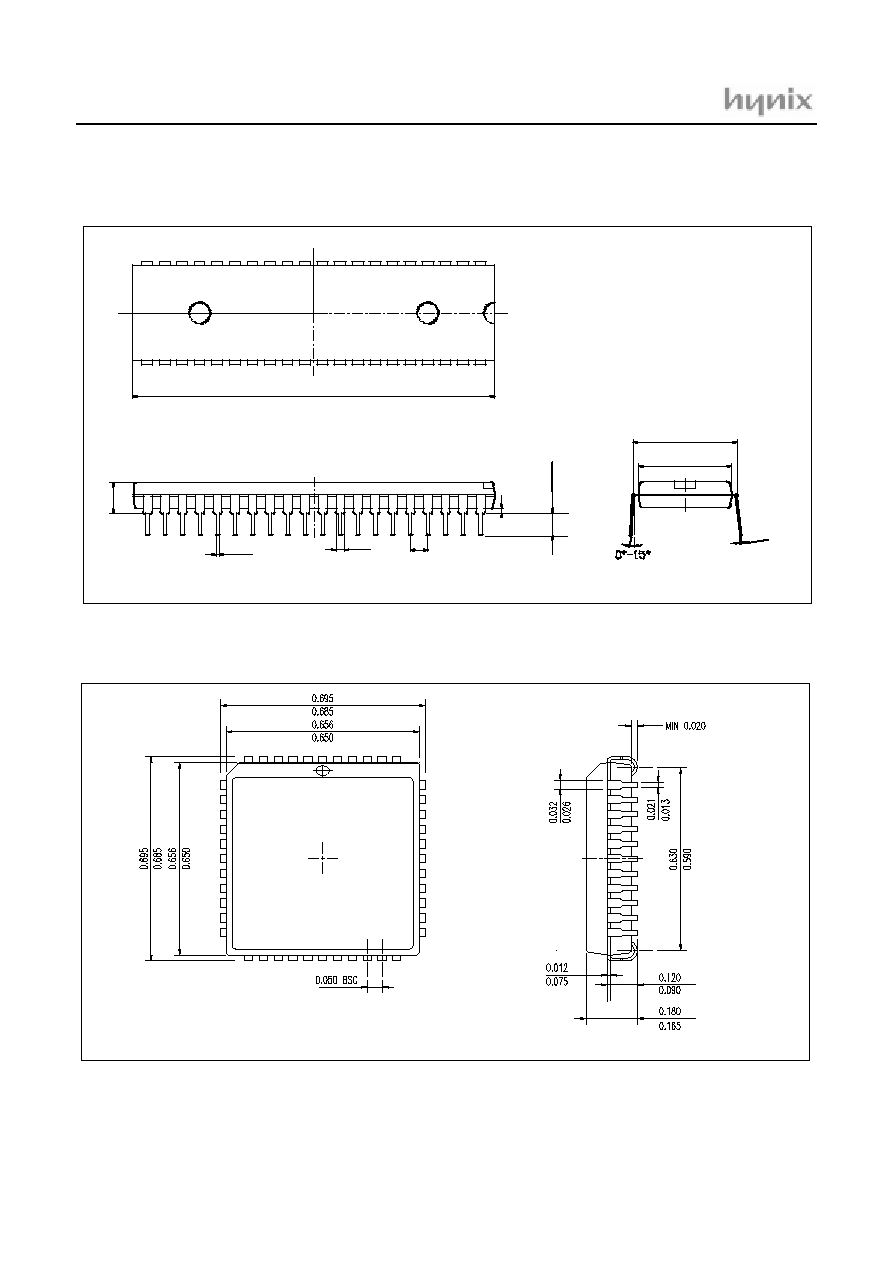
3. PIN ASSIGNMENT
28PIN
40PDIP
R00
1
R01
2
R02
3
R03
4
R04
5
R05
6
R06
7
R07
8
R34
9
R35
10
VDD
11
R36
12
R37
13
XOUT
14
XIN
15
R10
16
R11
17
R12
18
R15
19
RESETB
20
R14
REMOUT
R26
R25
R24
R23
R22
R21
R20
VSS
40
39
38
37
36
35
34
33
32
31
R33
R32
R31
R30
R17
R16
30
29
28
27
26
25
24
23
22
21
R13
R40
41
40
R00
R01
R24
R25
R26
R02
R03
R2
3
R04
R27
44PLCC
RESETB
REMOUT
R15
R12
R11
39
38
37
36
35
34
33
32
31
30
29
R40
R45
R10
R3
5
R3
4
R0
7
R0
6
18
19
20
21
22
23
24
25
26
27
28
VDD
R3
6
R3
7
XO
U
T
XI
N
R4
4
R0
5
7
8
9
10
11
12
13
14
R14
15
16
17
R4
2
R3
3
R2
0
R2
1
6
5
4
3
2
1
44
43
42
R3
2
R3
1
R3
0
R1
7
R2
2
VS
S
R16
R41
R13
R43
33
32
31
30
29
28
27
26
25
24
23
44QFP
22
21
20
19
18
17
16
15
14
13
12
1
2
3
4
5
6
7
8
9
10
11
34
35
36
37
38
39
40
41
42
43
44
R3
5
R3
4
R0
7
R0
6
VDD
R3
6
R3
7
XO
U
T
XI
N
R4
4
R0
5
R4
2
R3
3
R2
0
R2
1
R3
2
R3
1
R3
0
R1
7
R2
2
VS
S
R16
RESETB
REMOUT
R15
R12
R11
R40
R45
R10
R14
R41
R13
R00
R01
R24
R25
R26
R02
R03
R2
3
R04
R27
R43
1
2
3
4
5
6
7
8
9
10
11
12
13
14
15
16
17
18
19
20
28
27
26
25
24
23
22
21
R01
R02
R03
R04
R05
R06
R07
VDD
XOUT
XIN
R10
R11
R12
R13
R00
REMOUT
R25
R24
R23
R22
R21
R20
VSS
R17
R16
R15
R14
RESETB
R41
R27
HMS87C5216
Sep. 2001 Ver 1.0
5
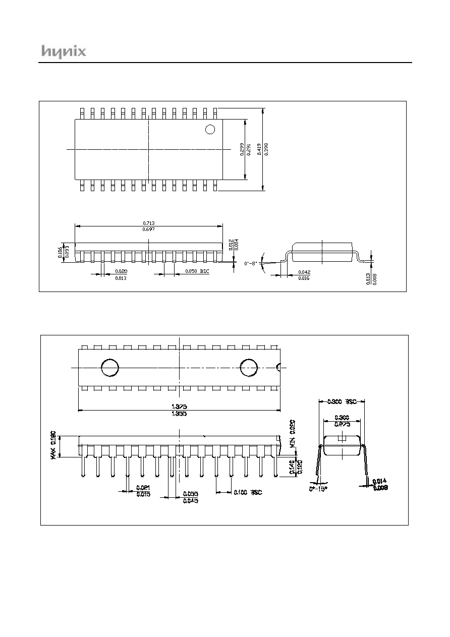
4. PIN DIAGRAM
HMS87C5216
6
Sep. 2001 Ver 1.0
2.045
2.075
0.065
0.015
0.022
0.
200
max.
0.530
0.550
0.045
0.100 BSC
0.600 BSC
0.
140
0.
120
MIN 0.
015
0.012
0.008

HMS87C5216
Sep. 2001 Ver 1.0
7

HMS87C5216
8
Sep. 2001 Ver 1.0
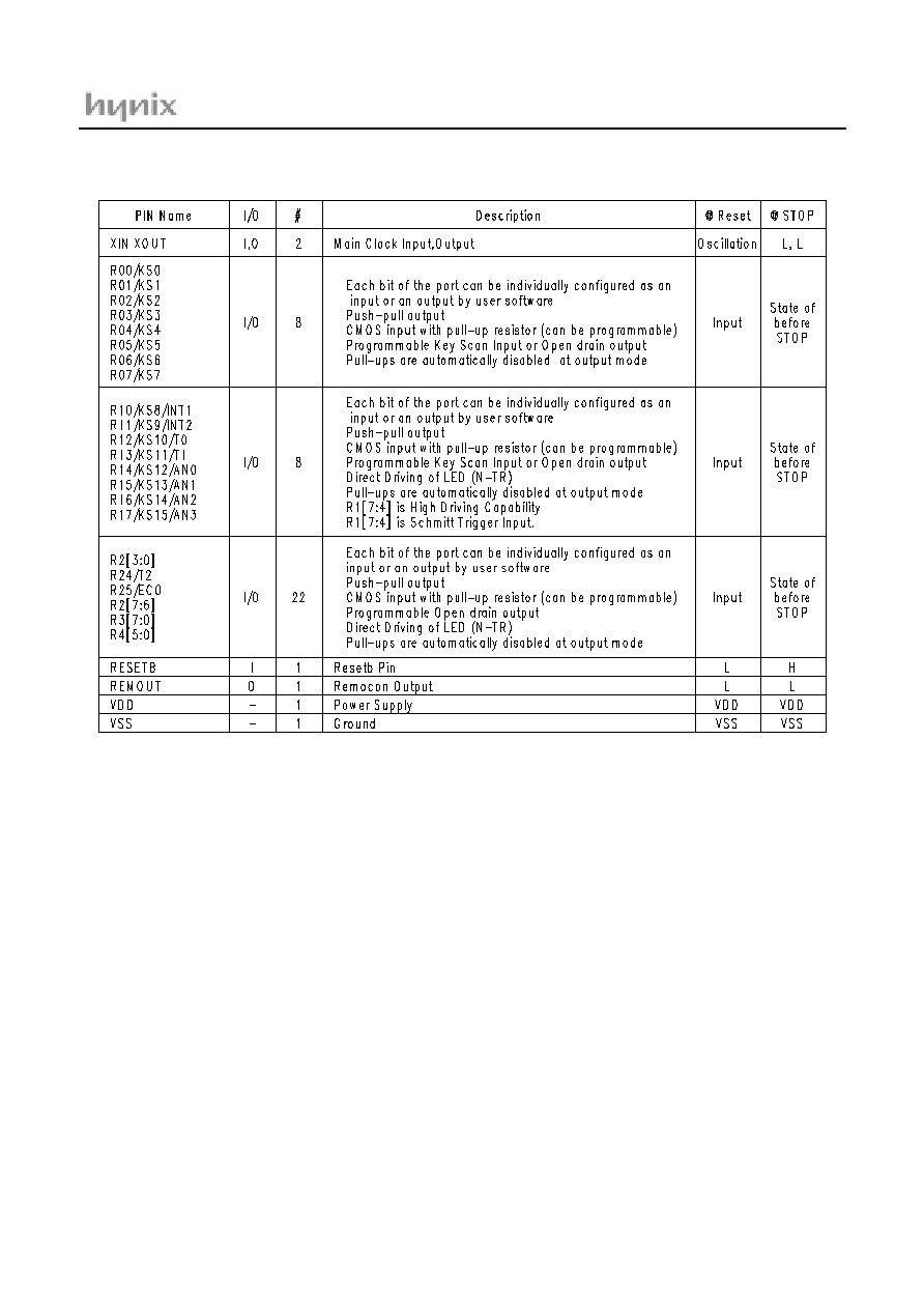
5. PIN FUNCTION
V
DD
: Supply voltage.
V
SS
: Circuit ground.
RESET: Reset the MCU.
X
IN
: Input to the inverting oscillator amplifier and input to
the internal main clock operating circuit.
X
OUT
: Output from the inverting oscillator amplifier.
R00~R07: R0 is an 8-bit CMOS bidirectional I/O port. R0
pins 1 or 0 written to the Port Direction Register can be
used as outputs or inputs.
R10~R17: R1 is an 8-bit CMOS bidirectional I/O port. R1
pins 1 or 0 written to the Port Direction Register can be
used as outputs or inputs.
In addition, R1 serves the functions of the various follow-
ing special features.
R20~R22, R30~R37 : R2 & R3 is a 8-bit CMOS bidirec-
tional I/O port. Each pins 1 or 0 written to the their Port Di-
rection Register can be used as outputs or inputs.
In addition, R2 serves the functions of the various follow-
ing special features.
R40~R43 : R4 is 1-bit CMOS bidirectional I/O port. This
pin 1 or 0 written to the its Port Direction Register can be
used as outputs or inputs.
Port pin
Alternate function
R10
R11
R12
R13
R14
R15
R16
R17
INT1 (External Interrupt input 1)
INT2 (External Interrupt input 2)
T0 (Timer / Counter inpit 0)
T1 (Timer / Counter inpit 1)
AN0 (ADC input 0)
AN1 (ADC input 1)
AN2 (ADC input 2)
AN3 (ADC input 3)
Port pin
Alternate function
R24
R25
T2 (Timer / Counter inpit 2)
/EC (Event Counter input )
HMS87C5216
Sep. 2001 Ver 1.0
9
6.
(
(
(
(
(
(
(
(
(
(
(
(
(
(
(
(
(
(
(
HMS87C5216
10
Sep. 2001 Ver 1.0
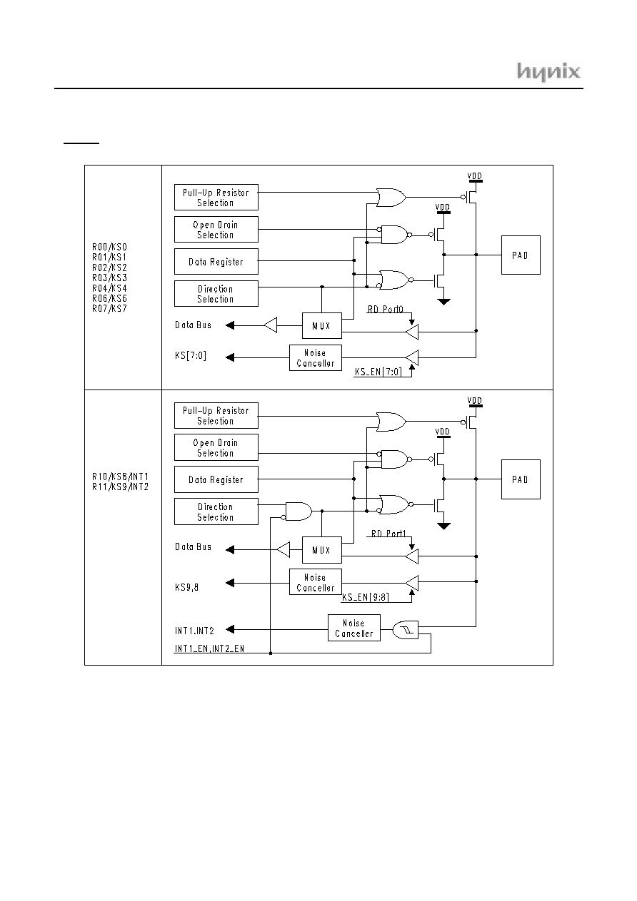
7. PORT STRUCTURES
∑ RESET
HMS87C5216
Sep. 2001 Ver 1.0
11
∑ Xin, Xout
⁄Þ \
HMS87C5216
12
Sep. 2001 Ver 1.0
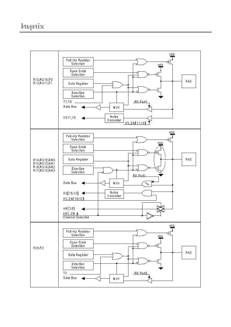
∑ RA0/EC0
⁄Þ \
HMS87C5216
Sep. 2001 Ver 1.0
13
∑ RA1/AN1 ~ RA7/AN7
XIN
XOUT

HMS87C5216
14
Sep. 2001 Ver 1.0
8. ELECTRICAL CHARACTERISTICS (HMS87C5216/GMS81C1408)
8.1 Absolute Maximum Ratings
Supply voltage ........................................... -0.3 to +7.0 V
Storage Temperature ................................-40 to +125
∞
C
aximum current out of V
SS
pin..........................TBD mA
Maximum current into V
DD
pin ........................TBD mA
Maximum current sunk by (I
OL
per I/O Pin) ....TBD mA
Maximum output current sourced by (I
OH
per I/O Pin)
...........................................................................TBD mA
Maximum current (
I
OL
) ...................................TBDmA
Maximum current (
I
OH
) ...................................TBDmA
Note: Stresses above those listed under "Absolute Maxi-
mum Ratings" may cause permanent damage to the
device. This is a stress rating only and functional op-
eration of the device at any other conditions above
those indicated in the operational sections of this
specification is not implied. Exposure to absolute
maximum rating conditions for extended periods
may affect device reliability.
8.2 Recommended Operating Conditions
8.3 A/D Converter Characteristics
(T
A
=25
∞
C, V
SS
=0V, V
DD
=3.072V @
f
XIN
=4MHz)
8.4 DC Electrical Characteristics
(T
A
=-20~85
∞
C for HMS87C5216/1408 or T
A
=-40~85
∞
C for HMS87C5216E/1408E, V
DD
=2.2~5.5V
,
V
SS
=0V)
,
Parameter
Symbol
Condition
Specifications
Unit
Min.
Max.
Supply Voltage
V
DD
f
XIN
=4MHz
2.0
5.5
V
Operating Frequency
f
XIN
V
DD
=2.0~5.5V
1
4
MHz
Operating Temperature
T
OPR
V
DD
=2.0~5.5V
-20 85
∞
C
Parameter
Symbol
Condition
Specifications
Unit
Min.
Typ.
Max.
Analog Input Voltage Range
V
AIN
-
V
SS-
0.3
-
V
DD
+0.3
V
Current Following Between AVdd and AVss
IAVdd
-
-
-
200
uA
Overall Accuracy
N
ACC
-
-
±
1.0
±
2.0
LSB
Non-Linearity Error
N
NLE
-
-
±
1.0
±
2.0
LSB
Differential Non-Linearity Error
N
DNLE
-
-
±
1.0
±
2.0
LSB
Zero Offset Error
N
ZOE
-
±
0.5
±
1.5
LSB
Full Scale Error
N
FSE
-
±
0.25
±
0.5
LSB
Gain Error
N
NLE
-
±
1.0
±
1.5
LSB
Conversion Time
T
CONV
f
XIN
=4MHz
-
-
30
uS
Parameter
Symbol
Pin
Condition
Specifications
Unit
Min.
Typ.
Max.
Input High Voltage
V
IH1
X
IN
, RESET
0.8 V
DD
-
V
DD
V
HMS87C5216
Sep. 2001 Ver 1.0
15
Input High Voltage
V
IH1
RESET,XIN,INT1,IN
T2,EC0,R1<7:4>
0.8V
DD
-
V
DD
V
V
IH2
R0,R1,R2,R3,R4
0.7V
DD
-
V
DD
V
Input Low Voltage
V
IL1
RESET,XIN,INT1,IN
T2,EC0,R1<7:4>
0
-
0.2V
DD
V
V
IL2
R0,R1,R2,R3,R4
0
-
0.3V
DD
V
Input High
Leakage Current
I
IH
R0,R1,R2,R3,R4
RESETB
V
IH
=VDD
-
-
1.0
µ
A
Input Low
Leakage Current
I
IL
R0,R1,R2,R3,R4
V
IL
=0V
-
-
-1.0
µ
A
Output High Voltage
V
OH1
R0,R1<3:0>,R2,R3,
R4
Ioh1=-0.8mA,VDD=3V
VDD-0.4
-
-
V
V
OH2
R1<7:0>,
I
oh2=-2.0mA,VDD=3V
VDD-0.4
-
-
V
V
OH3
XOUT
Ioh3=-50uA,VDD=3V
VDD-0.5
-
-
V
Output Low Voltage
V
OL1
R0,R1<3:0>,R2,R3,
R4
I
OL
=5mA,V
DD
=3V
-
-
0.8
V
V
OL2
XOUT
I
OL
=50uA,V
DD
=3V
-
-
0.5
V
Output High
Leakage Current
I
IOHL
R0,R1,R2,R3,R4
V
OH
=VDD
-
-
1.0
µ
A
Output Low
Leakage Current
I
IOLL
R0,R1,R2,R3,R4
V
OL
=0V
-
-
-1.0
µ
A
Output High Current
I
OH
REMOUT
VDD=3V,VOH=2.0V
-20
-
-5
mA
Output Low Current
I
OL
REMOUT
VDD=3V,VOL=1.0V
-0.5
-
3
mA
Input Pull-up
I
P
R0,R1,R2,R3,R4
RESETB
V
DD
=3V
50
100
200
Hysteresis
| V
T
|
Hysteresis Input
1
V
DD
=5V
0.5
-
-
V
Feed Back Resistor
RF!
M ain O S C Feedback
R esistor
V
DD
=3.0V, f
XIN
=4MHz
0.2
-
1.0
Supply Currnet
I
DD
Active Mode
V
DD
=4.0V
-
4.0
10
mA
V
DD
=2.0V
-
2.4
6
mA
I
sleep
Sleep Mode
V
DD
=4.0V
-
2.0
3.0
mA
V
DD
=2.0V
-
1.0
2.0
mA
I
stop
Stop Mode,Osc Stop
V
DD
=4.0V
-
5.0
30
µ
A
V
DD
=2.0V
-
3.0
25
µ
A
Parameter
Symbol
Pin
Condition
Specifications
Unit
Min.
Typ.
Max.
HMS87C5216
16
Sep. 2001 Ver 1.0
8.5 AC Characteristics
(T
A
=-20~85
∞
C for HMS87C5216/1408 or T
A
=-40~85
∞
C for HMS87C5216E/1408E, V
DD
=5V
±
10%
,
V
SS
=0V)
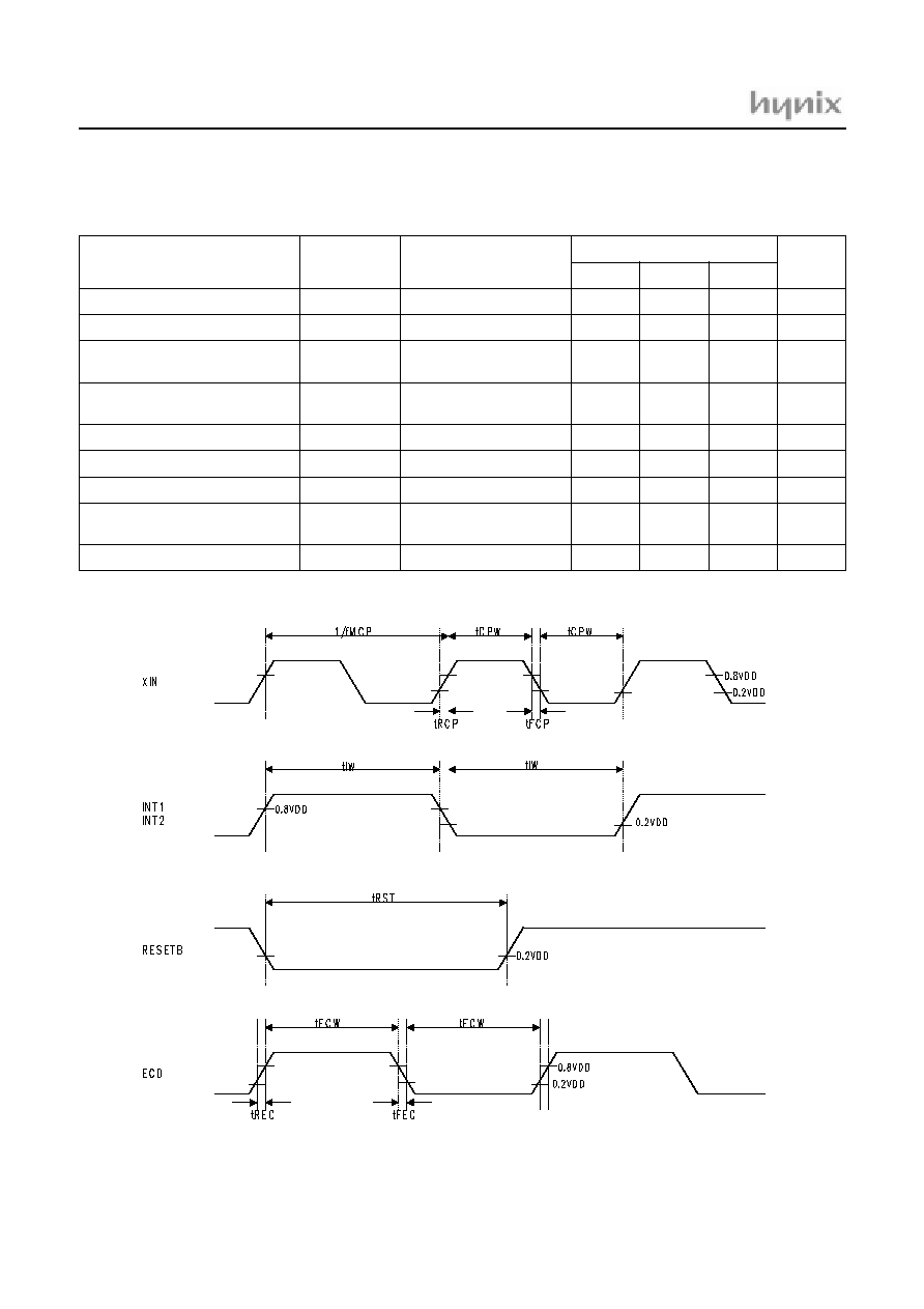
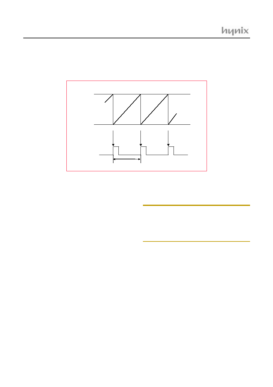
Figure 8-1 Timing Chart
Parameter
Symbol
Pins
Specifications
Unit
Min.
Typ.
Max.
Operating Frequency
f
MCP
X
IN
1
-
4
MHz
Systemp Clock Cycle Time
t
SYS
-
0.5
-
2.0
uS
Oscillation Stabilizing
Time(4MHz)
t
MST!
X
IN
, X
OUT
-
-
20
mS
External Clock "H" or "L" Pulse
Width
t
CPW
X
IN
80
nS
External Clock Transition Time
t
RCP,
t
FCP
X
IN
-
-
20
nS
Interrupt Input Pulse Width
t
lW
INT1,INT2
2
-
t
SYS
RESETB Input Pulse "L" Width
t
RST
RESETB
8
-
-
t
SYS
Event Couter Input "H" or "L"
Pulse Width
t
TCW
ECo
2
-
-
t
SYS
Event Couter Transition Time
t
REC,
t
FEC
ECo
0
-
20
nS
HMS87C5216
Sep. 2001 Ver 1.0
17
9. MEMORY ORGANIZATION
The HMS87C5216 have separate address spaces for Pro-
gram memory and Data Memory. Program memory can
only be read, not written to. It can be up to 16K bytes of
Program memory. Data memory can be read and written to
up to 320 bytes including the stack area.
9.1 Registers
This device has six registers that are the Program Counter
(PC), a Accumulator (A), two index registers (X, Y), the
Stack Pointer (SP), and the Program Status Word (PSW).
The Program Counter consists of 16-bit register.
Figure 9-1 Configuration of Registers
Accumulator: The Accumulator is the 8-bit general pur-
pose register, used for data operation such as transfer, tem-
porary saving, and conditional judgement, etc.
The Accumulator can be used as a 16-bit register with Y
Register as shown below.
Figure 9-2 Configuration of YA 16-bit Register
X, Y Registers: In the addressing mode which uses these
index registers, the register contents are added to the spec-
ified address, which becomes the actual address. These
modes are extremely effective for referencing subroutine
tables and memory tables. The index registers also have in-
crement, decrement, comparison and data transfer func-
tions, and they can be used as simple accumulators.
Stack Pointer: The Stack Pointer is an 8-bit register used
for occurrence interrupts and calling out subroutines. Stack
Pointer identifies the location in the stack to be accessed
(save or restore).
Generally, SP is automatically updated when a subroutine
call is executed or an interrupt is accepted. However, if it
is used in excess of the stack area permitted by the data
memory allocating configuration, the user-processed data
may be lost.
The stack can be located at any position within 100
H
to
17F
H
of the internal data memory. The SP is not initialized
by hardware, requiring to write the initial value (the loca-
tion with which the use of the stack starts) by using the ini-
tialization routine. Normally, the initial value of "17F
H
" is
used.
Note: The Stack Pointer must be initialized by software be-
cause its value is undefined after RESET.
Example: To initialize the SP
LDX
#07FH
TXSP
; SP
7F
H
Program Counter: The Program Counter is a 16-bit wide
which consists of two 8-bit registers, PCH and PCL. This
counter indicates the address of the next instruction to be
executed. In reset state, the program counter has reset rou-
tine address (PC
H
:0FF
H
, PC
L
:0FE
H
).
Program Status Word: The Program Status Word (PSW)
contains several bits that reflect the current state of the
CPU. The PSW is described in Figure 9-3 . It contains the
Negative flag, the Overflow flag, the Break flag the Half
Carry (for BCD operation), the Interrupt enable flag, the
Zero flag, and the Carry flag.
[Carry flag C]
This flag stores any carry or borrow from the ALU of CPU
after an arithmetic operation and is also changed by the
Shift Instruction or Rotate Instruction.
[Zero flag Z]
This flag is set when the result of an arithmetic operation
or data transfer is "0" and is cleared by any other result.
A
ACCUMULATOR
X REGISTER
Y REGISTER
STACK POINTER
PROGRAM COUNTER
PROGRAM STATUS
WORD
X
Y
SP
PCL
PCH
PSW
Two 8-bit Registers can be used as a "YA" 16-bit Register
Y
A
Y
A
SP
1
Stack Address (100
H
~17F
H
)
15
0
8
7
Hardware fixed
HMS87C5216
18
Sep. 2001 Ver 1.0
Figure 9-3 PSW (Program Status Word) Register
[Interrupt disable flag I]
This flag enables/disables all interrupts except interrupt
caused by Reset or software BRK instruction. All inter-
rupts are disabled when cleared to "0". This flag immedi-
ately becomes "0" when an interrupt is served. It is set by
the EI instruction and cleared by the DI instruction.
[Half carry flag H]
After operation, this is set when there is a carry from bit 3
of ALU or there is no borrow from bit 4 of ALU. This bit
can not be set or cleared except CLRV instruction with
Overflow flag (V).
[Break flag B]
This flag is set by software BRK instruction to distinguish
BRK from TCALL instruction with the same vector ad-
dress.
[Overflow flag V]
This flag is set to "1" when an overflow occurs as the result
of an arithmetic operation involving signs. An overflow
occurs when the result of an addition or subtraction ex-
ceeds +127(7F
H
) or -128(80
H
). The CLRV instruction
clears the overflow flag. There is no set instruction. When
the BIT instruction is executed, bit 6 of memory is copied
to this flag.
[Negative flag N]
This flag is set to match the sign bit (bit 7) status of the re-
sult of a data or arithmetic operation. When the BIT in-
struction is executed, bit 7 of memory is copied to this flag.
[Direct page flag G]
This flag assigns RAM page for direct addressing mode. In
the direct addressing mode, addressing area is from zero
page 00 to FF when this flag is 0. If it is set to 1, addressing
area is 1 page. It is set by instruction and cleared by
CLRG.
N
NEGATIVE FLAG
V
G
B
H
I
Z
C
MSB
LSB
RESET VALUE: 00
H
PSW
OVERFLOW FLAG
SELECT DIRECT PAGE FLAG
CARRY FLAG RECEIVES
ZERO FLAG
INTERRUPT ENABLE FLAG
CARRY OUT
HALF CARRY FLAG RECEIVES
CARRY OUT FROM BIT 1 OF
ADDITION OPERLANDS
BRK FLAG
HMS87C5216
Sep. 2001 Ver 1.0
19
9.2 Program Memory
A 16-bit program counter is capable of addressing up to
64K bytes, but these devices have 16K bytes program
memory space only physically implemented. Accessing a
location above FFFF
H
will cause a wrap-around to 0000
H
.
Figure 9-4 , shows a map of Program Memory. After reset,
the CPU begins execution from reset vector which is stored
in address FFFE
H
and FFFF
H
as shown in Figure 9-5 .
As shown in Figure 9-4 , each area is assigned a fixed lo-
cation in Program Memory. Program Memory area con-
tains the user program.
Figure 9-4 Program Memory Map
Page Call (PCALL) area contains subroutine program to
reduce program byte length by using 2 bytes PCALL in-
stead of 3 bytes CALL instruction. If it is frequently called,
it is more useful to save program byte length.
Table Call (TCALL) causes the CPU to jump to each
TCALL address, where it commences the execution of the
service routine. The Table Call service area spaces 2-byte
for every TCALL: 0FFC0
H
for TCALL15, 0FFC2
H
for
TCALL14, etc., as shown in Figure 9-6 .
Example: Usage of TCALL
The interrupt causes the CPU to jump to specific location,
where it commences the execution of the service routine.
The External interrupt 0, for example, is assigned to loca-
tion 0FFFA
H
. The interrupt service locations spaces 2-byte
interval: 0FFF8
H
and 0FFF9
H
for External Interrupt 1,
0FFFA
H
and 0FFFB
H
for External Interrupt 0, etc.
As for the area from 0FF00
H
to 0FFFF
H
, if any area of
them is not going to be used, its service location is avail-
able as general purpose Program Memory.
Figure 9-5 Interrupt Vector Area
PROGRAM
MEMORY
TCALL
AREA
INTERRUPT
VECTOR AREA
C000H
FEFFH
FF00H
FFC0H
FFDFH
FFE0H
FFFFH
PCALL
AREA
F000H
LDA
#5
TCALL
0FH
;
1BYTE INSTR UCTIO N
:
;
INSTEAD O F 3 BYTES
:
;
NO R M AL C ALL
;
;TABLE CALL ROUTINE
;
FUNC_A:
LDA
LRG0
RET
;
FUNC_B:
LDA
LRG1
RET
;
;TABLE CALL ADD. AREA
;
ORG
0FFC0H
;
TCALL ADDRESS AREA
DW
FUNC_A
DW
FUNC_B
1
2
0FFE0
H
E2
Address
Vector Area Memory
E4
E6
E8
EA
EC
EE
F0
F2
F4
F6
F8
FA
FC
FE
-
-
ADC Interrupt Vector Area
RC WT Interrupt Vector Area
WDT Interrupt Vector Area
-
Timer/Counter 2 Interrupt Vector Area
Timer/Counter 0 Interrupt Vector Area
-
EXT2 Interrupt Vector Area
KEY SCAN Interrupt Vector Area
-
RESET Vector Area
EXT1 Interrupt Vector Area
Timer/Counter 1 Interrupt Vector Area
BIT Interrupt Vector Area
"-" means reserved area.
NOTE:
HMS87C5216
20
Sep. 2001 Ver 1.0
Figure 9-6 PCALL and TCALL Memory Area
PCALL
rel
4F35
PCALL 35H
TCALL
n
4A
TCALL
4
0FFC0
H
C1
Address
Program Memory
C2
C3
C4
C5
C6
C7
C8
0FF00
H
Address
PCALL Area Memory
0FFFF
H
PCALL Area
(256 Bytes)
* means that the BRK software interrupt is using
same address with TCALL0.
NOTE:
TCALL 15
TCALL 14
TCALL 13
TCALL 12
TCALL 11
TCALL 10
TCALL 9
TCALL 8
TCALL 7
TCALL 6
TCALL 5
TCALL 4
TCALL 3
TCALL 2
TCALL 1
TCALL 0 / BRK *
C9
CA
CB
CC
CD
CE
CF
D0
D1
D2
D3
D4
D5
D6
D7
D8
D9
DA
DB
DC
DD
DE
DF
4F
~
~
~
~
NEXT
35
0FF35H
0FF00H
0FFFFH
11111111 11010110
01001010
PC:
F
H
F
H
D
H
6
H
4A
~
~
~
~
25
0FFD6H
0FF00H
0FFFFH
F1
NEXT
0FFD7H
˛
¿
√
0F125H
Reverse

HMS87C5216
Sep. 2001 Ver 1.0
21
Example: The usage software example of Vector address and the initialize part.
ORG
0FFE0H
DW
NOT_USED
; (0FFEO)
DW
NOT_USED
; (0FFE2)
DW
ADC_INT
; (0FFE4) A/D Interface
DW
RC_WT_INT
; (0FFE6) RC WAKE UP Timer
DW
BIT_INT
; (0FFE8) BIT Timer
DW
WDT_INT
; (0FFEA) WDT
DW
NOT_USED
; (0FFEC)
DW
TMR2_INT
; (0FFEE) Timer-2
DW
TMR1_INT
; (0FFF0) Timer-1
DW
TMR0_INT
; (0FFF2) Timer-0
DW
NOT_USED
; (0FFF4)
DW
EXT2_INT
; (0FFF6) External2
DW
EXT1_INT
; (0FFF8) External1
DW
KEY_SCAN
; (0FFFA) Key Scan
DW
NOT_USED
; (0FFFC)
DW
RESET
; (0FFFE) Reset
ORG
0F000H
;********************************************
;
MAIN PROGRAM
*
;*******************************************
;
RESET:
DI
;Disable All Interrupts
LDX
#0
RAM_CLR: LDA
#0
;RAM Clear(!0000H->!00BFH)
STA
{X}+
CMPX
#0C0H
BNE
RAM_CLR
;
LDX
#07FH
;Stack Pointer Initialize
TXSP
;
CALL
INITIAL
;
;
LDM
R1, #0
;Normal Port A
LDM
R1DD,#1000_0010B
;Normal Port Direction
LDM
R2, #0
;Normal Port B
LDM
R2DD,#1000_0010B
;Normal Port Direction
:
:
:
:
HMS87C5216
22
Sep. 2001 Ver 1.0
9.3 Data Memory
Figure 9-7 shows the internal Data Memory space availa-
ble. Data Memory is divided into two groups, a user RAM
(including Stack) and control registers.
Figure 9-7 Data Memory Map
User Memory
The HMS87C5216 has 330
◊
8 bits for the user memory
(RAM).
Control Registers
The control registers are used by the CPU and Peripheral
function blocks for controlling the desired operation of the
device. Therefore these registers contain control and status
bits for the interrupt system, the timer/ counters, analog to
digital converters and I/O ports. The control registers are in
address range of 0C0
H
to 0FF
H
.
Note that unoccupied addresses may not be implemented
on the chip. Read accesses to these addresses will in gen-
eral return random data, and write accesses will have an in-
determinate effect.
More detailed informations of each register are explained
in each peripheral section.
Note: Write only registers can not be accessed by bit ma-
nipulation instruction. Do not use read-modify-write
instruction. Use byte manipulation instruction.
Example; To write at CKCTLR
LDM
CKCTLR,#09H ;Divide ratio
˜
16
Note: Several names are given at same address. Refer to-
USER
MEMORY
CONTROL
REGISTERS
0000H
00BFH
00C0H
00FFH
PAGE0
USER
MEMORY
(including STACK)
0100H
017FH
PAGE2
Address
Symbol
R/W
RESET
Value
Addressing
m ode
Table 9-1 Control Registers
HMS87C5216
Sep. 2001 Ver 1.0
23
below table.
Stack Area
The stack provides the area where the return address is
saved before a jump is performed during the processing
routine at the execution of a subroutine call instruction or
the acceptance of an interrupt.
When returning from the processing routine, executing the
subroutine return instruction [RET] restores the contents of
the program counter from the stack; executing the interrupt
return instruction [RETI] restores the contents of the pro-
gram counter and flags.
The save/restore locations in the stack are determined by
the stack pointed (SP). The SP is automatically decreased
after the saving, and increased before the restoring. This
means the value of the SP indicates the stack location
number for the next save.
Address
Symbol
R/W
RESET
Value
Addressing
mode
0C0H
0C1H
0C2H
0C3H
0C4H
0C5H
0C6H
0C7H
0C7H
0C8H
0C9H
0CAH
0CBH
0CCH
0CDH
0CEH
0CFH
R0
R0DR
R1
R1DR
R2
R2DR
TMR1
CKCTLR
BITR
WDTR
PSR
RCWTR
IESR
IENL
IRQL
IENH
IRQH
R/W
W
R/W
W
R/W
W
W
W
R
W
W
W
W
R/W
R/W
R/W
R/W
Undefined
0000_0000
Undefined
0000_0000
Undefined
0000_0000
0000_0000
--11_0111
0000_0000
-000_1111
--00_0000
----_1000
--00_00--
-000_-0--
-000_-0--
000-_000-
000-_000-
byte, bit
1
byte
2
byte, bit
byte
byte, bit
byte
byte
byte
byte
byte
byte
byte,bit
byte,bit
byte,bit
byte,bit
byte,bit
byte,bot
0D0H
0D1H
0D2H
0D3H
0D4H
0D5H
0D5H
0D6H
0D6H
0D7H
0D8H
0D8H
0D9H
0D9H
0DAH
0DCH
0DDH
0DEH
0DFH
TM0
TM1
TM2
T0HMD
T0HLD
T0MC
T0LMD
T0LC
T0LLD
T1HD
T1C
T1LD
T2C
T2D
TM01
KSR0
KSR1
R10D
R2OD
R/W
R/W
R/W
W
W
R
W
R
W
W
R
W
R
W
R/W
W
W
W
W
0000_0000
0000_-000
---0_0000
Undefined
Undefined
0000_0000
Undefined
0000_0000
Undefined
Undefined
0000_0000
Undefined
0000_0000
Undefined
0000_0000
00000_000
0000_0000
0000_0000
0000_0000
byte, bit
byte, bit
byte, bit
byte
byte
byte
byte
byte
byte
byte
byte
byte
byte
byte
byte
byte
byte
byte
byte,bit
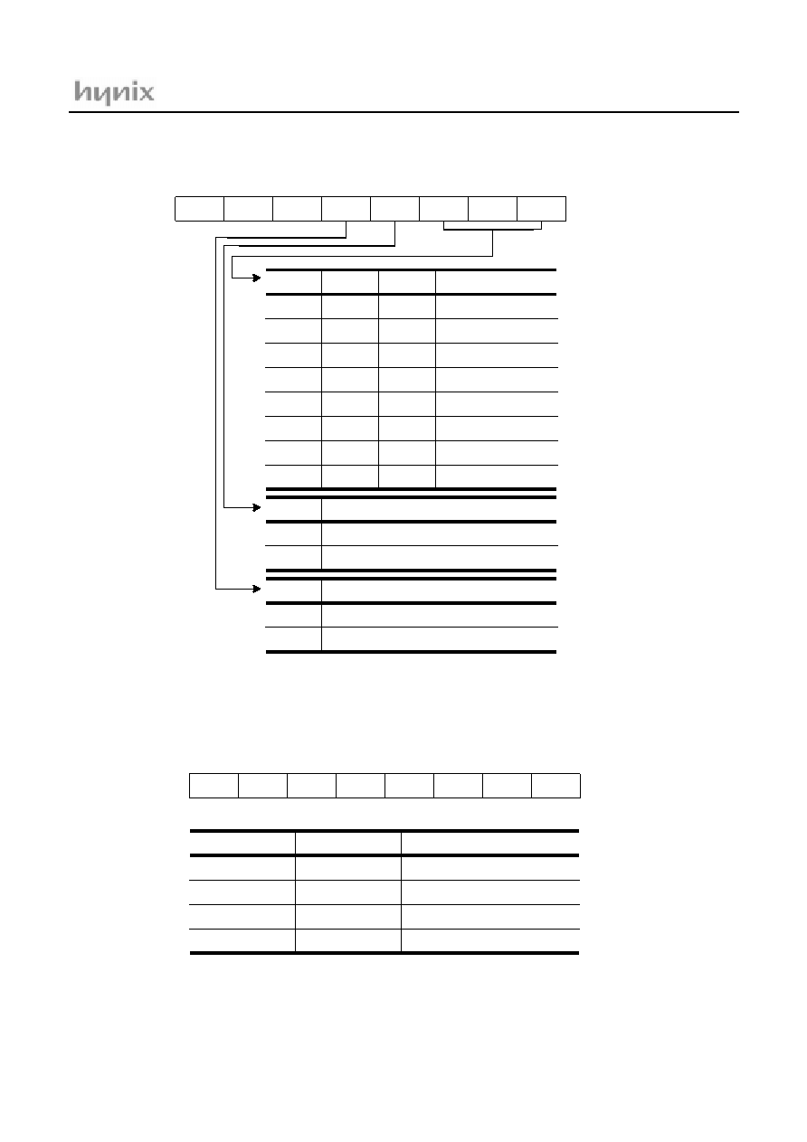
0E0H
0E1H
0E4H
0E5H
0E6H
0E7H
0E8H
0EEH
0EFH
R3OD
R4OD
R0OD
R3
R3DR
R4
R4DR
TMR2
LVDR
W
W
W
R/W
W
R/W
W
R
R
0000_0000
--00_0000
0000_0000
Undefined
0000_0000
Undefined
66
00_0000
0000_0000
666
_
6
00
6
byte
byte
byte
byte
5
bit
byte
byte,bit
byte
byte
byte
Table 9-1 Control Registers
0F0H
0F4H
0F5H
0F6H
0F7H
0F8H
0F9H
0FAH
0FBH
0FCH
SMR
ADMR
ADDR
KRL0
KRL1
R0PU
R1PU
R2PU
R3PU
R4PU
W
R/W
R
W
W
W
W
W
W
W
----_---0
-000_0001
Undefined
0000_0000
0000_0000
0000_0000
0000_0000
0000_0000
0000_0000
--00_0000
byte
byte, bit
byte
byte
byte
byte
byte
byte
byte
byte
1. "byte, bit" means that register can be addressed by not only bit
but byte manipulation instruction.
2. "byte" means that register can be addressed by only byte
manipulation instruction. On the other hand, do not use any
read-modify-write instruction such as bit manipulation for
clearing bit.
Table 9-1 Control Registers
HMS87C5216
24
Sep. 2001 Ver 1.0
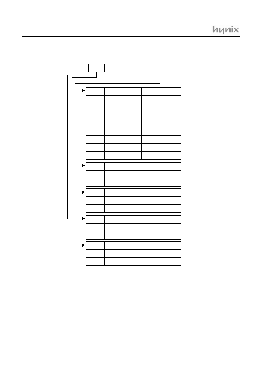
9.4 Addressing Mode
The HMS87C5216 and GMS81C1408 uses six addressing
modes;
∑ Register addressing
∑ Immediate addressing
∑ Direct page addressing
∑ Absolute addressing
∑ Indexed addressing
∑ Register-indirect addressing
(1) Register Addressing
Register addressing accesses the A, X, Y, C and PSW.
(2) Immediate Addressing
#imm
In this mode, second byte (operand) is accessed as a data
immediately.
Example:
0435
ADC
#35H
E45535
LDM
35H,#55H
(3) Direct Page Addressing
dp
In this mode, a address is specified within direct page.
Example;
C535
LDA
35H
;A
RAM[35H]
(4) Absolute Addressing
!abs
Absolute addressing sets corresponding memory data to
Data, i.e. second byte(Operand I) of command becomes
lower level address and third byte (Operand II) becomes
upper level address.
With 3 bytes command, it is possible to access to whole
memory area.
ADC, AND, CMP, CMPX, CMPY, EOR, LDA, LDX,
LDY, OR, SBC, STA, STX, STY
Example;
0735F0
ADC
!0F035H
;A
ROM[0F035H]
35
A+35H+C
A
04
MEMORY
E4
0F100
H
data
55H
~
~
~
~
data
0035
H
˛
35
0F102
H
55
0F101
H
¿
data
35
0035
H
0F551
H
data
A
¿
˛
~
~
~
~
C5
0F550
H
07
0F100
H
~
~
~
~
data
0F035
H
˛
F0
0F102
H
35
0F101
H
¿
A+data+C
A
address: 0F035
HMS87C5216
Sep. 2001 Ver 1.0
25
The operation within data memory (RAM)
ASL, BIT, DEC, INC, LSR, ROL, ROR
Example; Addressing accesses the address 0135
H
.
983500
INC
!0035H
;A
RAM[035H]
(5) Indexed Addressing
X indexed direct page (no offset)
{X}
In this mode, a address is specified by the X register.
ADC, AND, CMP, EOR, LDA, OR, SBC, STA, XMA
Example; X=15
H
D4
LDA
{X}
;ACC
RAM[X].
X indexed direct page, auto increment
{X}+
In this mode, a address is specified within direct page by
the X register and the content of X is increased by 1.
LDA, STA
Example; X=35
H
DB
LDA
{X}+
X indexed direct page (8 bit offset)
dp+X
This address value is the second byte (Operand) of com-
mand plus the data of
-register. And it assigns the mem-
ory in Direct page.
ADC, AND, CMP, EOR, LDA, LDY, OR, SBC, STA
STY, XMA, ASL, DEC, INC, LSR, ROL, ROR
Example; X=015
H
C645
LDA
45H+X
98
0F100
H
~
~
~
~
data
0035
H
˛
00
0F102
H
35
0F101
H
¿
data+1
data
√
address: 0035
data
D4
15
H
0E550
H
data
A
¿
˛
~
~
~
~
data
DB
35
H
data
A
¿
˛
~
~
~
~
36H
X
data
45
5A
H
0E551
H
data
A
¿
˛
~
~
~
~
C6
0E550
H
45H+15H=5AH
√
HMS87C5216
26
Sep. 2001 Ver 1.0
Y indexed direct page (8 bit offset)
dp+Y
This address value is the second byte (Operand) of com-
mand plus the data of Y-register, which assigns Memory in
Direct page.
This is same with above (2). Use Y register instead of X.
Y indexed absolute
!abs+Y
Sets the value of 16-bit absolute address plus Y-register
data as Memory. This addressing mode can specify mem-
ory in whole area.
Example; Y=55
H
D500FA
LDA
!0FA00H+Y
(6) Indirect Addressing
Direct page indirect
[dp]
Assigns data address to use for accomplishing command
which sets memory data(or pair memory) by Operand.
Also index can be used with Index register X,Y.
JMP, CALL
Example;
3F35
JMP
[35H]
X indexed indirect
[dp+X]
Processes memory data as Data, assigned by 16-bit pair
m e m o r y w h i c h i s d e t e r m i n e d b y p a i r d a t a
[dp+X+1][dp+X] Operand plus X-register data in Direct
page.
ADC, AND, CMP, EOR, LDA, OR, SBC, STA
Example; X=10
H
1625
ADC
[25H+X]
D5
0F100
H
data
A
˛
~
~
~
~
data
0FA55
H
0FA00H+55H=0FA55H
√
FA
0F102
H
00
0F101
H
¿
0A
35
H
jump to address 0E30A
H
˛
~
~
~
~
35
0FA00
H
E3
36
H
¿
3F
0E30A
H
NEXT
~
~
~
~
05
35
H
0E005
H
~
~
~
~
25
0FA00
H
E0
36
H
16
0E005
H
data
~
~
~
~
√
A + data + C
A
25 + X(10) = 35
H
˛
¿
HMS87C5216
Sep. 2001 Ver 1.0
27
Y indexed indirect
[dp]+Y
Processes memory data as Data, assigned by the data
[dp+1][dp] of 16-bit pair memory paired by Operand in Di-
rect page plus Y-register data.
ADC, AND, CMP, EOR, LDA, OR, SBC, STA
Example; Y=10
H
1725
ADC
[25H]+Y
Absolute indirect
[!abs]
The program jumps to address specified by 16-bit absolute
address.
JMP
Example;
1F25E0
JMP
[!0C025H]
05
25
H
0E005
H
+ Y(10) = 0E015
H
˛
~
~
~
~
25
0FA00
H
E0
26
H
¿
17
0E015
H
data
~
~
~
~
√
A + data + C
A
25
0E025
H
jump to
~
~
~
~
E0
0FA00
H
E7
0E026
H
¿
25
0E725
H
NEXT
~
~
~
~
1F
PROGRAM MEMORY
˛
address 0E30A
H
HMS87C5216
28
Sep. 2001 Ver 1.0
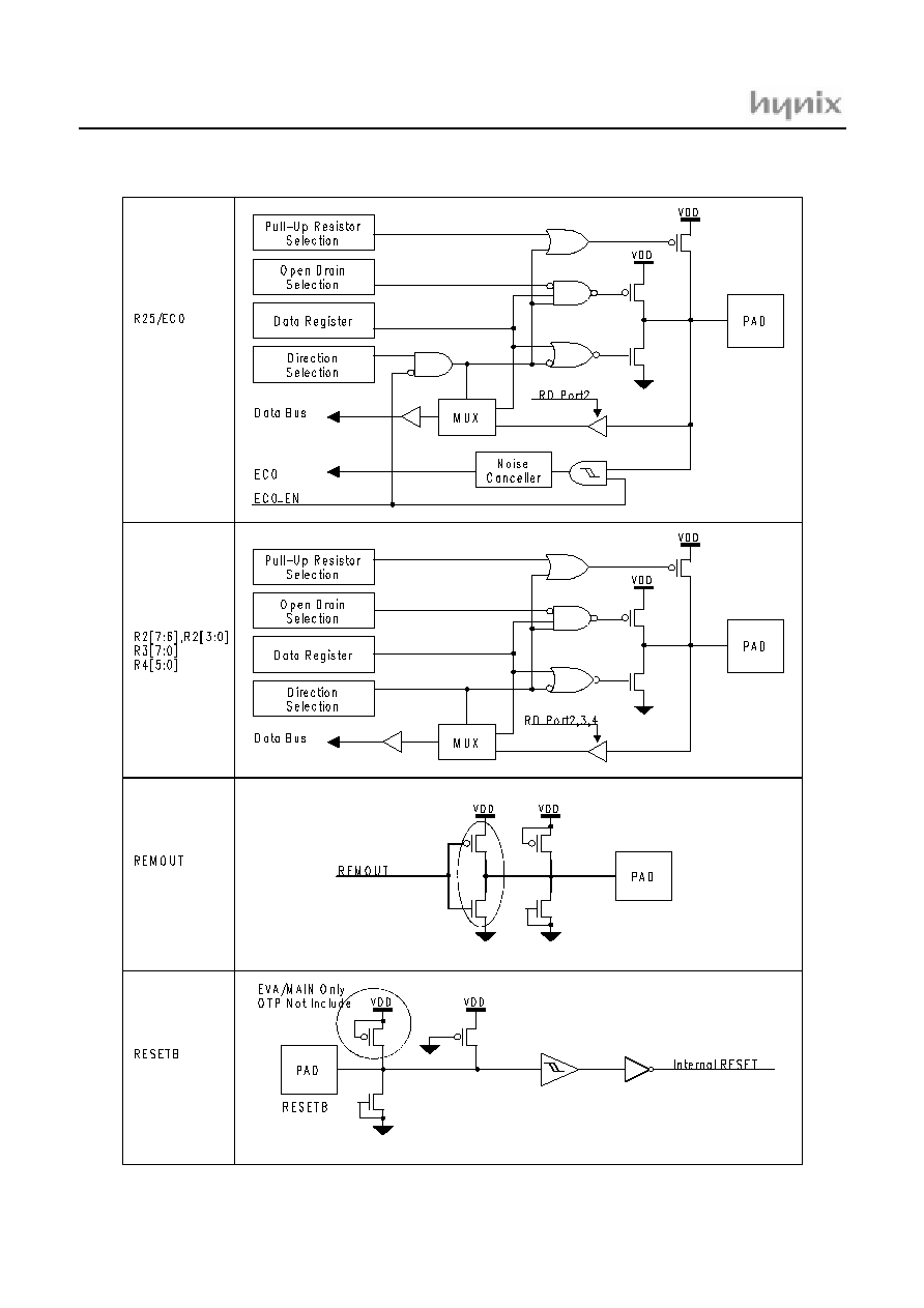
10. I/O PORTS
The GMS87C5216 has 38 I/O ports which are PORT0(8 I/
O), PORT1 (8 I/O), PORT2 (8 I/O), PORT3 (8 I/O),
PORT4 (6 I/O). Pull-up resistor of each port can be select-
able by program. Each port contains data direction register
which controls I/O and data register which stores port data
10.1 R0 Ports
R0 is an 8-bit CMOS bidirectional I/O port (address
0C0
H
). Each I/O pin can independently used as an input or
an output through the R0DD register (address 0C1
H
).
R0 has internal pull-ups that is independently connected or
disconnected by R0PC. The control registers for R0 are
shown below.
(1) R0 I/O Data Direction Register (R0DD)
R0 I/O Data Direction Register (R0DD) is 8-bit register,
and can assign input state or output state to each bit. If
R0DD is ``1``, port R0 is in the output state, and if ``0``, it
is in the input state. R0DD is write-only register. Since
R0DD is initialized as ``00 h`` in reset state, the whole port
R0 becomes input state.
(2) R0 Data Register (R0)
R0 data register (R0) is 8-bit register to store data of port
R0. When set as the output state by R0DD, and data is writ-
ten in R0, data is outputted into R0 pin. When set as the in-
put state, input state of pin is read. The initial value of R0
is unknown in reset state.
(3) R0 Open drain Assign Register (R0ODC)
R0 Open Drain Assign Register (R0ODC) is 8bit register,
and can assign R0 port as open drain output port each bit,
if corresponding port is selected as output. If R0ODC is
selected as ``1``, port R0 is open drain output, and if select-
ed as ``0``, it is push-pull output. R0ODC is write-only
register and initialized as ``00 h`` in reset state.
(4) R0 Pull-up Resistor Control Register (R0PC)
R0 pull-up resistor control register (R0PC) is 8-bit register
and can control pull-up on or off each bit, if corresponding
port is selected as input. If R0PC is selected as ``1``, pull-
up ia disabled and if selected as ``0``, it is enabled. R0PC
is write-only register and initialized as ``00 h`` in reset
state. The pull-up is automatically disabled, if correspond-
ing port is selected as output.
10.2 R1 Ports
R1 is an 8-bit CMOS bidirectional I/O port (address
0C2
H
). Each I/O pin can independently used as an input or
an output through the R1DD register (address 0C3
H
).
R1 has internal pull-ups that is independently connected or
disconnected by register R1PC. The control registers for
R1 are shown below.
R0 Data Register (R/W)
R0
ADDRESS : 0C0
H
RESET VALUE : Undefined
R07 R06 R05 R04 R03 R02 R01 R00
Port Direction
R0 Direction Register (W)
R0DD
ADDRESS : 0C1
H
RESET VALUE : 00
H
0: Input
1: Output
Pull-up select
R0 Pull-up Selection Register (W)
R0PC
ADDRESS :0F8
H
RESET VALUE : 00
H
1: Without pull-up
0: With pull-up
Open drain select
R0 Open drain Assign Register (W)
R0ODC
ADDRESS :0E4
H
RESET VALUE : 00
H
0: Push-pull
1: Open drain
HMS87C5216
Sep. 2001 Ver 1.0
29
(1) R1 I/O Data Direction Register (R1DD)
R1 I/O Data Direction Register (R1DD) is 8-bit register,
and can assign input state or output state to each bit. If
R1DD is ``1``, port R1 is in the output state, and if ``0``, it
is in the input state. R1DD is write-only register. Since
R1DD is initialized as ``00 h`` in reset state, the whole port
R1 becomes input state.
(2) R1 Data Register (R1)
R1 data register (R1) is 8-bit register to store data of port
R1. When set as the output state by R1DD, and data is writ-
ten in R1, data is outputted into R1 pin. When set as the in-
put state, input state of pin is read. The initial value of R1
is unknown in reset state.
(3) R1 Mode Register (PMR1)
R1 Port Mode Register (PMR1) is 8-bit register, and can
assign the selection mode for each bit. When set as ``0``,
corresponding bit of PMR1 acts as port R1 selection mode,
and when set as ``1``, it becomes function selection mode.
PMR1 is write-only register and initialized as ``00 h`` in
reset state. Therefore, becomes Port selection mode. Port
R1 can be I/O port by manipulating each R1DD bit, if cor-
responding PMR1 bit is selected as ``0``.
Table 10-1
Selection mode of PMR1
(4) R1 Pull-up Resistor Control Register (R1PC)
R1 pull-up resistor control register (R1PC) is 8-bit register
and can control pull-up on or off each bit, if corresponding
port is selected as input. If R1PC is selected as ``1``, pull-
up ia disabled and if selected as ``0``, it is enabled. R1PC
is write-only register and initialized as ``00 h`` in reset
state. The pull-up is automatically disabled, if correspond-
ing port is selected as output.
10.3 R2 Port
R2 is an 8-bit CMOS bidirectional I/O port (address
0C4
H
). Each I/O pin can independently used as an input or
an output through the R2DD register (address 0C5
H
).
R1 Data Register (R/W)
R1
ADDRESS : 0C2
H
RESET VALUE : Undefined
R17 R16 R15 R14 R13 R12 R11 R10
Port Direction
R1 Direction Register (W)
R1DD
ADDRESS : 0C3
H
RESET VALUE : 00
H
0: Input
1: Output
Pull-up select
R1 Pull-up Selection Register (W)
R1PC
ADDRESS : 0F9
H
RESET VALUE : 00
H
1: Without pull-up
0: With pull-up
Open drain select
R1 Open drain Assign Register (W)
P1ODC
ADDRESS : 0DE
H
RESET VALUE : 00
H
0: Push-pull
1: Open drain
Mode select
R1 Port Mode Register (W)
PMR1
ADDRESS : 0C9
H
RESET VALUE : 00
H
0: Port R1 selection
1: Function selection
Pin Name
PMR1
Selection
Mode
Remarks
-
-
EC0
0
R25(I/O)
-
1
EC0(I)
EVENT COUNT0
T2
0
R24(I/O)
-
1
T2(O)
TIMER2
T1
0
R13 (I/O)
-
1
T1(O)
TIMER1
T0
0
R12 (I/O)
-
1
T0(O)
TIMER0
INT2
0
R11 (I/O)
-
1
INT2(I)
EXT INT2
INT1
0
R10(I/O)
-
1
INT1(I)
EXT INT1
HMS87C5216
30
Sep. 2001 Ver 1.0
R2 has internal pujll-ups that is independently connected
or disconnected by R2PC (address 0FA
H
). The control reg-
isters for R2 are shown as below.
(1) R2 I/O Data Direction Register (R2DD)
R2 I/O Data Direction Register (R2DD) is 8-bit register,
and can assign input state or output state to each bit. If
R2DD is ``1``, port R2 is in the output state, and if ``0``, it
is in the input state. R2DD is write-only register. Since
R2DD is initialized as ``00 h`` in reset state, the whole port
R2 becomes input state.
(2) R2 Data Register (R2)
R2 data register (R2) is 8-bit register to store data of port
R2. When set as the output state by R2DD, and data is writ-
ten in R2, data is outputted into R2 pin. When set as the in-
put state, input state of pin is read. The initial value of R2
is unknown in reset state.
(3) R2 Open drain Assign Register (R2ODC)
R2 Open Drain Assign Register (R2ODC) is 8bit register,
and can assign R2 port as open drain output port each bit,
if corresponding port is selected as output. If R2ODC is
selected as ``1``, port R2 is open drain output, and if select-
ed as ``0``, it is push-pull output. R2ODC is write-only
register and initialized as ``00 h`` in reset state.
(4) R2 Pull-up Resistor Control Register (R2PC)
R2 pull-up resistor control register (R2PC) is 8-bit register
and can control pull-up on or off each bit, if corresponding
port is selected as input. If R2PC is selected as ``1``, pull-
up ia disabled and if selected as ``0``, it is enabled. R2PC
is write-only register and initialized as ``00 h`` in reset
state. The pull-up is automatically disabled, if correspond-
ing port is selected as output.
R2 Data Register (R/W)
R2
ADDRESS : 0C4
H
RESET VALUE : Undefined
R27 R26 R25 R24 R23 R22 R21 R20
Port Direction
R2 Direction Register (W)
R2DD
ADDRESS : 0C5
H
RESET VALUE : 00
H
0: Input
1: Output
Pull-up select
R2 Pull-up Selection Register (W)
R2PC
ADDRESS :0FA
H
RESET VALUE : 00
H
1: Without pull-up
0: With pull-up
Open drain select
R2 Open drain Assign Register (W)
R2ODC
ADDRESS :0DF
H
RESET VALUE : 00
H
0: Push-pull
1: Open drain
HMS87C5216
Sep. 2001 Ver 1.0
31
R3 Port
R3 is an 8-bit CMOS bidirectional I/O port (address
0E5
H
). Each I/O pin can independently used as an input or
an output through the R3DD register (address 0E6
H
).
R3 has internal pull-ups that is independently connected or
disconnected by R3PC (address 0FB
H
). The control regis-
ters for R3 are shown as below.
(1) R3 I/O Data Direction Register (R3DD)
R3 I/O Data Direction Register (R3DD) is 8-bit register,
and can assign input state or output state to each bit. If
R3DD is ``1``, port R3 is in the output state, and if ``0``, it
is in the input state. R3DD is write-only register. Since
R3DD is initialized as ``00 h`` in reset state, the whole port
R3 becomes input state.
(2) R3 Data Register (R3)
R3 data register (R3) is 8-bit register to store data of port
R3. When set as the output state by R3DD, and data is writ-
ten in R3, data is outputted into R3 pin. When set as the in-
put state, input state of pin is read. The initial value of R3
is unknown in reset state.
(3) R3 Open drain Assign Register (R3ODC)
R3 Open Drain Assign Register (R3ODC) is 8bit register,
and can assign R3 port as open drain output port each bit,
if corresponding port is selected as output. If R3ODC is
selected as ``1``, port R3 is open drain output, and if select-
ed as ``0``, it is push-pull output. R3ODC is write-only
register and initialized as ``00 h`` in reset state.
(4) R3 Pull-up Resistor Control Register (R3PC)
R3 pull-up resistor control register (R3PC) is 8-bit register
and can control pull-up on or off each bit, if corresponding
port is selected as input. If R3PC is selected as ``1``, pull-
up ia disabled and if selected as ``0``, it is enabled. R3PC
is write-only register and initialized as ``00 h`` in reset
state. The pull-up is automatically disabled, if correspond-
ing port is selected as output.
R3 Data Register (R/W)
R3
ADDRESS : 0E5
H
RESET VALUE : Undefined
R37 R36 R35 R34 R33 R32 R31 R30
Port Direction
R3 Direction Register (W)
R3DD
ADDRESS : 0E6
H
RESET VALUE : 00
H
0: Input
1: Output
Pull-up select
R3 Pull-up Selection Register (W)
R3PC
ADDRESS :0FB
H
RESET VALUE : 00
H
1: Without pull-up
0: With pull-up
Open drain select
R3 Open drain Assign Register (W)
R3ODC
ADDRESS :0E0
H
RESET VALUE : 00
H
0: Push-pull
1: Open drain
HMS87C5216
32
Sep. 2001 Ver 1.0
R4 Port
R4 is an 1-bit CMOS bidirectional I/O port (address
0E7
H
). Each I/O pin can independently used as an input or
an output through the R4DD register (address 0E8
H
).
R3 has internal pull-ups that is independently connected or
disconnected by R4PC (address 0FC
H
). The control regis-
ters for R4 are shown as below.
(1) R4 I/O Data Direction Register (R4DD)
R4 I/O Data Direction Register (R4DD) is 1-bit register,
and can assign input state or output state to each bit. If
R4DD is ``1``, port R4 is in the output state, and if ``0``, it
is in the input state. R4DD is write-only register. Since
R4DD is initialized as ``00 h`` in reset state, the whole port
R4 becomes input state.
(2) R4 Data Register (R4)
R4 data register (R4) is 1-bit register to store data of port
R4. When set as the output state by R4DD, and data is writ-
ten in R4, data is outputted into R4 pin. When set as the in-
put state, input state of pin is read. The initial value of R4
is unknown in reset state.
(3) R4 Open drain Assign Register (R4ODC)
R4 Open Drain Assign Register (R4ODC) is 1-bit register,
and can assign R4 port as open drain output port each bit,
if corresponding port is selected as output. If R4ODC is
selected as ``1``, port R4 is open drain output, and if select-
ed as ``0``, it is push-pull output. R4ODC is write-only
register and initialized as ``00 h`` in reset state.
(4) R4 Pull-up Resistor Control Register (R4PC)
R4 pull-up resistor control register (R4PC) is 1-bit register
and can control pull-up on or off each bit, if corresponding
port is selected as input. If R4PC is selected as ``1``, pull-
up ia disabled and if selected as ``0``, it is enabled. R4PC
is write-only register and initialized as ``00 h`` in reset
state. The pull-up is automatically disabled, if correspond-
ing port is selected as output.
R4 Data Register (R/W)
R4
ADDRESS : 0E7
H
RESET VALUE : Undefined
Port Direction
R4 Direction Register (W)
R4DD
ADDRESS : 0E8
H
RESET VALUE : 00
H
0: Input
1: Output
Pull-up select
R4 Pull-up Selection Register (W)
R4PC
ADDRESS :0FC
H
RESET VALUE : 00
H
1: Without pull-up
0: With pull-up
Open drain select
R4 Open drain Assign Register (W)
R4ODC
ADDRESS :0E1
H
RESET VALUE : 00
H
0: Push-pull
1: Open drain
R44 R43 R42 R41 R40
HMS87C5216
Sep. 2001 Ver 1.0
33
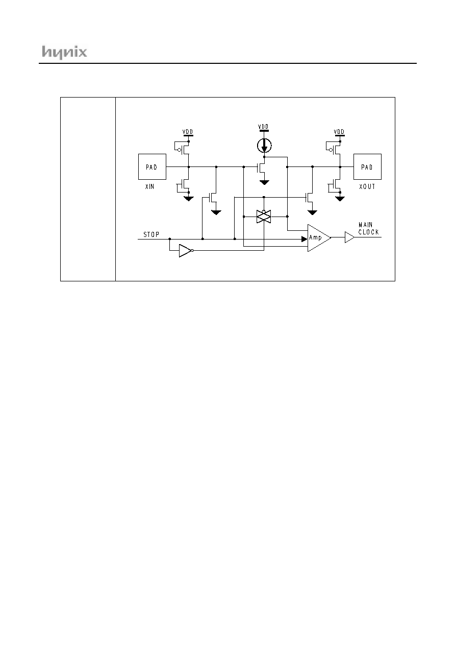
11. CLOCK GENERATOR
Clock generating circuit consists of Clock Pulse Generator
(C.P.G), Prescaler, Basic Interval Timer (B.I.T) and Watch
Dog Timer. The clock applied to the Xin pin divided by
two is used as the internal system clock.
Figure 11-1 Block Diagram of Clock Generator
Prescaler consists of 12-bit binary counter. The clock sup-
plied from oscillation circuit is input to prescaler (fex).
The divided output from each bit of prescaler is provided
to peripheral hardware.
Figure 11-2 Block diagram of Prescaler
9
PRESCALER
C.P.G
MUX
WDT (6)
COMPARATOR
Internal Data Bus
0
1
2
3
4
0
5
6
6
WDTON
To Reset
Circuit
IFWDT
WDTCL
IFBIT
5
0
7
0
fcpu
fex
PS1
ENPCK
Peripheral
CKCTLR
BTCL
3
8
OSC
Circuit
B.I.T (8)
6
WDTR
Internal System Clock
5
B.I.T
Peripheral
PS0
PS1
PS2
PS3
PS4
PS5
PS6
PS7
PS8
PS9
PS10 PS11
PS12
fex
ENPCK
fcpu
PS1
PS2
PS3
PS4
PS5
PS6
PS7
PS8
PS9
PS10
PS11
PS12

HMS87C5216
34
Sep. 2001 Ver 1.0
Table 11-1 ps output period
lock to peripheral hardware can be stopped by bit4 (EN-
PCK) of CKCTLR Register. ENPCK is set to ``1`` in reset
state.
fex (MHz)
4 MHz
2 MHz
frequency
period
frequency
period
ps 0
ps 1
ps 2
ps 3
ps 4
ps 5
ps 6
ps 7
ps 8
ps 9
ps 10
ps 11
ps 12
4 MHz
2 MHz
1 MHz
500 KHz
250 KHz
125 KHz
62.5 KHz
31.25 KHz
15.63 KHz
7.183 KHz
3.906 KHz
1.953 KHz
0.976 KHz
250 ns
500 ns
1 us
2 us
4 us
8 us
16 us
32 us
64 us
128 us
256 us
512 us
1024 us
2 MHz
1 MHz
500 KHz
250 KHz
125 KHz
62.5 KHz
31.25 KHz
15.63 KHz
7.183 KHz
3.906 KHz
1.953 KHz
0.976 KHz
0.488 KHz
500 ns
1 us
2 us
4 us
8 us
16 us
32 us
64 us
128 us
256 us
512 us
1024 us
2048 us
HMS87C5216
Sep. 2001 Ver 1.0
35
12. Timer
12.1 Basic Interval Timer
The GMS81C5016/24/32 has one 8-bit Basic Interval Tim-
er that is free-run and can not stop. Block diagram is shown
in Figure 12-1 .
The Basic Interval Timer generates the time base for key
scanning, watchdog timer counting, and etc. It also pro-
vides a Basic interval timer interrupt (IFBIT). As the count
overflow from FF
H
to 00
H
, this overflow causes the inter-
rupt to be generated.
-8bit binary counter
-Use the bit output of prescaler as input to secure the oscil-
lation stabilization time after power-on
-Secures the oscillation stabilization time in standby mode
(stop mode) release
-Contents of B.I.T can be read
-Provides the clock for watch dog timer.
Figure 12-1 Block Diagram of Basic Interval Timer
(1) Control of B.I.T
The Basic Interval Timer is controlled by the clock control
register (CKCTLR) shown in Figure 12-2 . If bit3(BTCL)
of CKCTLR is set to ``1``, B.I.T is cleared, and then, after
one machine cycle, BTCL becomes ``0``, and B.I.T starts
counting. BTCL is set to ``0`` in reset state.
MUX
BITR
IFBIT
PS3
PS4
PS5
PS6
PS7
PS8
PS9
PS10
DATA BUS
DATA BUS
-
-
WDTON
ENPCK
BTCL
BTS2
BTS1
BTS0
CKCTLR
BIT0
BIT1
BIT2
BIT3
BIT4
BIT5
BIT6
BIT7
HMS87C5216
36
Sep. 2001 Ver 1.0
Figure 12-2 BTCL mode of B.I.T
(2) Input clock selection of B.I.T
The input clock of B.I.T can be selected from the prescaler
within a range of 2us to 256us by clock input selection bits
(BTS2~BTS0). (at fex = 4MHz). In reset state, or power
on reset, BTS2=``1``, BTS1=``1``, BTS0=``1`` to secure
the longest oscillation stabilization time. B.I.T can gener-
ate the wide range of basic interval time interrupt request
(IFBIT) by selecting prescaler output. Interrupt interval
can be selected to kinds of interval time as shown in
Figure 12-3 .
Figure 12-3 Basic Interval Timer Interrupt Time
(3) Reading Basic Interval Timer
By reading of the Basic Interval Timer Register (BITR),
we can read counter value of B.I.T. Because B.I.T can be
cleared or read, the spending time up to maximum 65.5ms
can be available. B.I.T is read-only register. If B.I.T reg-
0
-
-
WDTON
ENPCK
BTCL
BTS2
BTS1
BTS0
7
W <00C7 h>
CKCTLR
Clock Control Register
BTCL
Periphral clock
0
1
free-run
Automatically cleared, after one cycle
512 us
1,024 us
2,048 us
4,096 us
8,192 us
16,384 us
32,768 us
65,536 us
0
-
-
WDTON
ENPCK
BTCL
BTS2
BTS1
BTS0
7
W <00C7 h>
CKCTLR
Clock Control Register
BTS0
B.I.T. Input clock
0
1
BTS1
0
0
BTS2
0
0
Standby release time
0
1
0
1
1
0
0
0
1
1
0
1
0
1
1
1
1
1
PS3 (2us)
PS4 (4us)
PS5 (8us)
PS6 (16us)
PS7 (32us)
PS8 (64us)
PS9 (128us)
PS10 (256us)

HMS87C5216
Sep. 2001 Ver 1.0
37
ister is written, then CKCTLR register with same address
is written.
12.2 Timer0, Timer1, Timer2
(1) Timer Operation Mode
Timer consists of 16bit binary counter Timer0 (T0), 8bit
binary Timer1 (T1), Timer2 (T2), Timer Data Register,
Timer Mode Register (TM01, TM0, TM1, TM2) and con-
trol circuit. Timer Data Register Consists of Timer0 High-
MSB Data Register (T0HMD), Timer0 High-LSB Data
Register (T0HLD), Timer0 Low-MSB Data Register
(T0LMD), Timer0 Low-LSB Data Register (T0LLD),
Timer1 High Data Register (T1HD), Timer1 Low Data
Register (T1LD), Timer2 Data Register (T2DR). Any of
the PS0 ~ PS5, PS11 and external event input EC can be
selected as clock source for T0. Any of the PS0 ~ PS3, PS7
~ PS10 can be selected as clock T1. Any of the PS5 ~ PS12
can be selected as clock source for T2.
* Relevant Port Mode Register (PMR1 : 00C9 h) value
should be assigned for event counter,
0
BIT7
BIT6
BIT5
BIT4
BIT3
BIT2
BIT1
BIT0
7
R <00C7 h>
BITR
Basic Interval Timer Register
Timer0
- 16-bit Interval Timer
- 16-bit Event Counter
- 16-bit Input Capture
- 16-bit rectangular-wave output
- Single/Modulo-N Mode
- Timer Output Initial Value Setting
- Timer0~Timer1 combination Logic Output
- One Interrupt Generating Every 2nd
Counter Overflow
Timer1
- 8-bit Interval Timer
- 8-bit rectangular-wave output
Timer2
- 8-bit Interval Timer
- 8-bit rectangular-wave output
- Modulo-N Mode
HMS87C5216
38
Sep. 2001 Ver 1.0
Figure 12-4 Timer / Counter Block diagram
(2) Function of Timer & Counter
T2 OUT / R15
TIMER0 (16 BIT)
Polarity
Selection
T0HMD
T0HLD
T0LMD
T0LLD
Tout LOGIC
T1HD
T1LD
TIMER1 (8 BIT)
EDGE
Selection
T1 OUT / R16
REMOUT
T0 OUT / R17
EC / R14
INT2 / R12
(Capture
Signal)
16
8
8
8
8
8
8
16
TIMER2 (8 BIT)
T2DR
PS0 ( 0.25 us)
16,384 us
PS0 ( 0.25 us)
64 us
PS5 ( 8 us)
2.048 us
PS1 ( 0. 5 us)
32,768 us
PS1 ( 0.5 us)
128 us
PS6 ( 16 us)
4,096 us
PS2 ( 1 us)
65,536 us
PS2 ( 1 us)
256 us
PS7 ( 32 us)
8,192 us
PS3 ( 2 us)
131,072 us
PS3 ( 2 us)
512us
PS8 ( 64 us)
16,384 us
PS4 ( 4 us)
262,144 us
PS7 ( 32 us)
8,192 us
PS9 ( 128 us)
32,768 us
PS5 ( 8 us)
524,288 us
PS8 ( 64 us)
16,384 us
PS10 ( 256 us)
65,536 us
PS11 ( 512 us)
33,554,432 us
PS9 ( 128 us)
32,768 us
PS11 ( 512 us)
131,072 us
EC
-
PS10 ( 256 us)
65,536 us
PS12 (1,024 us)
262,144 us
fex = 4MHz
16bit Timer (T0)
8bit Timer (T1)
8bit Timer (T2)
Resolution (CK)
Max. Count
Resolution (CK)
Max. Count
Resolution (CK)
Max. Count
HMS87C5216
Sep. 2001 Ver 1.0
39
Figure 12-5 Block Diagram of Timer0
Internal Data Bus
TIMER0 H
COUNT
REG
TIMER0 L
COUNT
REG
TIMER0
HM
DATA
REG
TIMER0
HL
DATA
REG
TIMER0
LM
DATA
REG
TIMER0
LL
DATA
REG
SINGLE/
MODULO-N
SELECTION
MUX
CK
T0 COUNTER
(16 BIT)
Clear
PS0
PS1
PS2
PS3
PS4
PS5
PS11
EC
M
U
X
D
E
L
A
Y
EDGE
SELECTION
MUX
Int.
Gen.
OUTPUT GEN.
TM0
R / W
<00D0 h>
<00D5 h>
<00D6 h>
<00D3 h>
<00D4 h>
<00D5 h>
<00D6 h>
16
16
16
INT2
T0INT
T0 OUT
IFT0
DATA READ
7
6
5
4
3
2
1
0
HMS87C5216
40
Sep. 2001 Ver 1.0
Figure 12-6 Block Diagram of Timer1
Internal Data Bus
7
6
5
4
3
2
1
0
TIMER1
COUNT REG
TIMER1
H
DATA
REG
TIMER1
L
DATA
REG
SINGLE/
MODULO-N
SELECTION
MUX
CK
T1 COUNTER
(8 BIT)
PS0
PS1
PS2
PS3
PS7
PS8
PS9
PS10
Int.
Gen.
OUTPUT GEN.
TM1
R/W
<00D1h>
<00D7 h>
<00D8 h>
T1OUT
IFT1
OUTPUT GEN.
X
<00D8 h>
T1INT
HMS87C5216
Sep. 2001 Ver 1.0
41
Figure 12-7 Block Diagram of Timer2
Internal Data Bus
7
6
5
4
3
2
1
0
TIMER2
COUNT REG
MUX
CK
T2 COUNTER
(8 BIT)
PS5
PS6
PS7
PS8
PS9
PS10
PS11
PS12
OUTPUT GEN.
TM2
R/W
<00D2 h>
<00D9 h>
T2 OUT
<00D9 h>
TIMER2
DATA REG
IFT2
HMS87C5216
42
Sep. 2001 Ver 1.0
Figure 12-8 Timer0 / Timer1 Mode Register
0
TOUTS
TOUTB
-
T0OUTP
T0INIT
T1INIT
TOUT1
TOUT0
7
R / W <00DA h>
TM01
Timer0 / Timer1 Mode Register
TOUT0
TOUT1
TOUT LOGIC
0
0
0
1
1
0
1
1
T1INIT
Timer1 Output Initial Value
0
1
T0INIT
0
1
T0OUTP
T0OUT Polarity Selection
0
1
TOUTB
REMOUT Port Bit Control
0
1
TOUTS
REMOUT Port Output Selection
(TOUT logic or TOUTB)
0
1
AND of T0 OUTPUT and T1 OUTPUT
NAND of T0 OUTPUT and T1 OUTPUT
OR of T0 OUTPUT and T1 OUTPUT
NOR of T0 OUTPUT and T1 OUTPUT
Timer1 output low
Timer1 output high
Timer0 Output Initial Value
Timer0 Output Low
Timer0 Output High
T0OUT polarity equal to TOUT logic input signal
T0OUT polarity reverse to TOUT logic input signal
REMOUT output low
REMOUT output high
Bit (TOUTB) output through REMOUT
TOUT logic output through REMOUT
HMS87C5216
Sep. 2001 Ver 1.0
43
Figure 12-9 Timer0 Mode Register
0
CAP0
T0ST
T0CN
T0MOD
T0IFS
T0SL2
T0SL1
T0SL0
7
R / W <00D0 h>
TM0
Timer0 Mode Register
T0SL2
T0SL1
Input clock selection
0
0
0
0
0
1
0
1
T0IFS
Timer0 Interrupt Selection
0
1
1
0
1
0
1
1
1
1
T0SL0
0
1
0
1
0
1
0
1
Notes
PS0 (250ns)
PS1 (500ns)
PS2 ( 1us)
PS3 ( 2us)
PS4 ( 4us)
PS5 ( 8us)
PS11 (512us)
EC
Event
Counter
*
Interrupt every counter overflow
Interrupt every 2nd counter overflow
T0MOD
Timer0 Single/Modulo-N Selection
0
1
Modulo-N
Single
T0CN
Timer0 Counter Continuation/Pause Control
0
1
Count pause
Count contination
T0ST
Timer0 Start/Stop Control
0
1
Timer0 Stop
Timer Start after clear
CAP0
Timer0 Interrupt Selection
0
1
Timer/Counter
Input capture *
* PS1 : not supporting input capture.
HMS87C5216
44
Sep. 2001 Ver 1.0
Figure 12-10 Timer1 Mode Register
0
T1ST
T1CN
T1MOD
T1IFS
-
T1SL2
T1SL1
T1SL0
7
R / W <00D1 h>
TM1
Timer1 Mode Register
T1SL2
T1SL1
Input clock selection
0
0
0
0
0
1
0
1
T1IFS
Timer1 Interrupt Selection
0
1
1
0
1
0
1
1
1
1
T1SL0
0
1
0
1
0
1
0
1
PS0 (250ns)
PS1 (500ns)
PS2 ( 1us)
PS3 ( 2us)
PS7 ( 32us)
PS8 ( 64us)
PS9 (128us)
Interrupt every counter overflow
Interrupt every 2nd counter overflow
T1MOD
Timer1 Single/Modulo-N Selection
0
1
Modulo-N
Single
T1CN
Timer1 Counter Continuation/Pause Control
0
1
Count pause
Count contination
T1ST
Timer1 Start/Stop Control
0
1
Timer1 Stop
Timer1 Start after clear
PS10 (256us)
HMS87C5216
Sep. 2001 Ver 1.0
45
Figure 12-11 Timer2 Mode Register
Figure 12-12 External Interrupt Signal Edge Selection Register
0
-
-
-
T2ST
T2CN
T2SL2
T2SL1
T2SL0
7
R / W <00D2 h>
TM2
Timer2 Mode Register
T2SL2
T2SL1
Input clock selection
0
0
0
0
0
1
0
1
1
0
1
0
1
1
1
1
T2SL0
0
1
0
1
0
1
0
1
PS5 ( 8us)
PS6 ( 16us)
PS7 ( 32us)
PS8 ( 64us)
PS9 ( 128us)
PS10 ( 256us)
PS11 ( 512us)
T2CN
Timer2 Counter Continuation/Pause Control
0
1
Count pause
Count contination
T2ST
Timer2 Start/Stop Control
0
1
Timer2 Stop
Timer2 Start after clear
PS12 (1024us)
IED*H
IED*L
INT*
0
-
-
IED2H
IED2L
IED1H
IED1L
-
-
7
W <00CB h>
IEDS
External Interrupt Signal Edge Selection Register
0
0
0
1
1
1
0
1
-
Falling Edge Selection
Rising Edge Selection
Both Edge Selection
HMS87C5216
46
Sep. 2001 Ver 1.0
(3) Timer0, Timer1
TIMER0 and TIMER1 have an up-counter. When value of
the up-counter reaches the content of Timer Data Register
(TDR), the up-counter is cleared to ``00 h``, and interrupt
(IFT0, IFT1) is occured at the next clock.
Figure 12-13 Operatiion of Timer0
For Timer0, the internal clock (PS) and the external clock
(EC) can be selected as counter clock. But Timer1 and
Timer2 use only internal clock. As internal clock. Timer0
can be used as internal-timer which period is determined
by Timer Data Register (TDR). Chosen as external
clock, Timer0 executes as event-counter. The counter ex-
ecution of Timer0 and Timer1 is controlled by T0CN,
T0ST, CAP0, T1CN, T1ST, of Timer Mode Register TM0
and TM1. T0CN, T1CN are used to stop and start Timer0
and Timer1 without clearing the counter. T0ST, T1ST is
used to clear the counter. For clearing and starting the
counter, T0ST or T1ST should be temporarily set to ``0``
and then set to ``1``. T0CN, T1CN, T0ST and T1ST
should be set ``1``, when Timer counting-up. Controlling
of CAP0 enables Timer0 as input capture. By program-
ming of CAP0 to ``1``, the period of signal from INT2 can
be measured and then, event counter value for INT2 can
be read. During counting-up, value of counter can be read.
Timer execution is stopped by the reset signal (RESET
= ``L``)
Note: In the process of reading 16-bit Timer Data, first
read the upper 8-bit data. Then read the lower 8-bit data,
and read the upper 8-bit data again. If the earlier read up-
per 8-bit data are matched with the later read upper 8-bit
data, read 16-bit data are correct. If not, caution should be
taken in the selection of upper 8-bit data.
(Example)
1) Upper 8-bit Read 0A 0A
2) Lower 8-bit Read FF 01
3) Upper 8-bit Read 0B 0B
=====================
- -
0AFF 0B01
Concurrence
Concurrence
Concurrence
CLEAR
CLEAR
CLEAR
0
T0 Data
Registers
Value
T0 Value
INTERRUPT
INTERRUPT
INTERRUPT
Interval period
IFT0
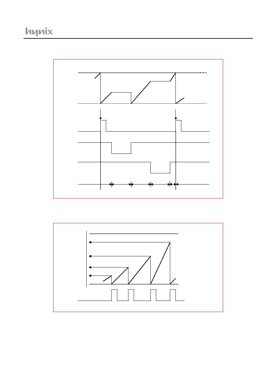
HMS87C5216
Sep. 2001 Ver 1.0
47
Figure 12-14 Start/Stop operation of Timer0
Figure 12-15 Input capture operation of Timer0
Concurrence
CLEAR
INTERRUPT
Concurrence
CLEAR
INTERRUPT
IFT0
T0ST
T0CN
0
0
1
0
1
Counter
Count
Stop
Clear
& Count
Stop
Count
continue
Clear & Start
T0 Data
Register
Value
T0 Value
Clear & Start
T0
T1
T2
T3
INT2
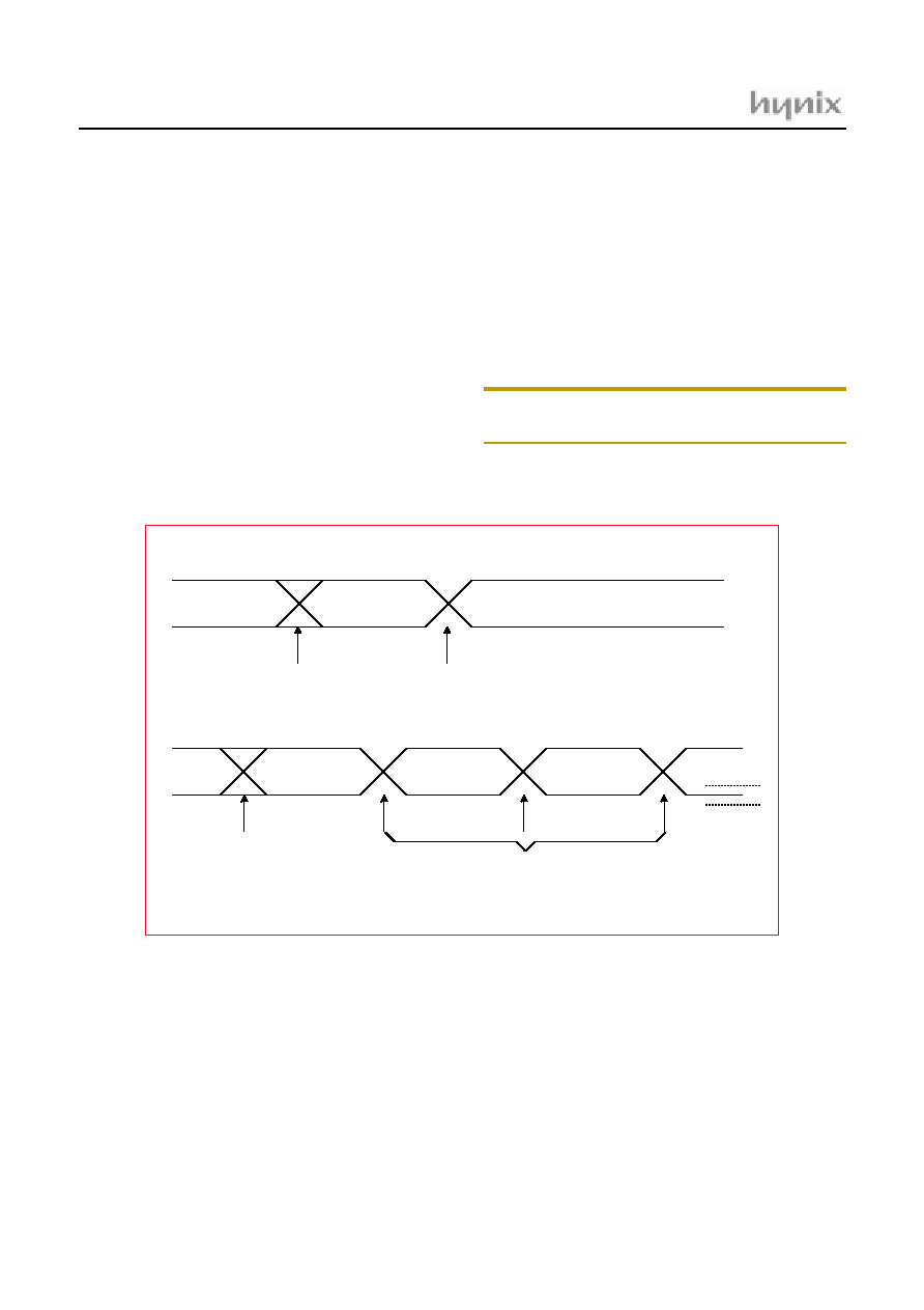
HMS87C5216
48
Sep. 2001 Ver 1.0
* Single/Modulo-N Mode
Timer0 (Timer1) can select initial (T0INIT, T1INIT of
TM01) output level of Timer Output port. If initial level is
``L``, Low-Data Register value of Timer Data Register is
transferred to comparator and T0OUT (T1OUT) is to be
``Low``, if initial level is High? High -Data Register is
transferred and to be ``High``. Single Mode can be set by
Mode Select bit (T0MOD, T1MOD) of Timer Mode Reg-
ister (TM0, TM1) to ``1`` When used as Single Mode,
Timer counts up and compares with value of Data Regis-
ter. If the result is same, Time Out interrupt occurs and
level of Timer Output port toggle, then counter stops as re-
set state. When used as Modulo-N Mode, T0MOD
(T1MOD) should be set ``0``. Counter counts up until the
value of Data Register and occurs Time-out interrupt. The
level of Timer Output port toggle and repeats process of
counting the value which is selected in Data Register.
During Modulo-N Mode, If interrupt select bit (T0IFS,
T1IFS) of Mode Register is ``0``, Interrupt occurs on ev-
ery Time-out. If it is ``1``, Interrupt occurs every second
time-out.
Note: (*note. Timer Output is toggled whenever time
out happen)
Figure 12-16 Operation Diagram for Single/Modulo-N Mode
(4) Timer 2
Timer2 operates as a up-counter. The content of T2DR are
compared with the contents of up-counter. If a match is
found. Timer2 interrupt (IFT2) is generated and the up-
counter is cleared to ``00 h``. Therefore, Timer2 executes
as a interval timer. Interrupt period is determined by the
count source clock for the Timer2 and content of T2DR.
When T2ST is set to ``1``, count value of Timer 2 is
cleared and starts counting-up. For clearing and starting
the Timer2. T2ST have to set to ``1`` after set to ``0``. In
order to write a value directly into the T2DR, T2ST should
be set to ``0``. Count value of Timer2 can be read at any
time.
8bit / 16bit
counting
8bit / 16bit
counting
Timer Enable initial.
value toggle.
Timer-output toggle.
interrupt occurs.
count stop.
Timer Enable initial.
value toggle.
Timer-Output Toggle.
Int occurs (IFS = 1) Each 2nd time out.
Int occurs (IFS = 0) When Time out.
[ Single Mode ]
[ Modulo-N Mode ]
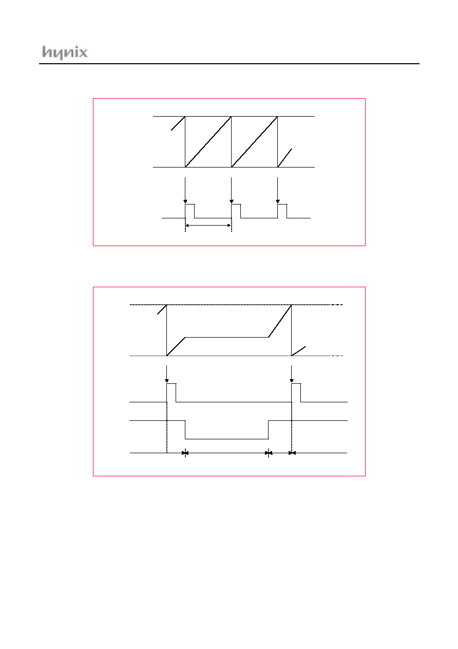
HMS87C5216
Sep. 2001 Ver 1.0
49
Figure 12-17 Operation of Timer2
Figure 12-18 Start/Stop of Timer2
Concurrence
Concurrence
Concurrence
CLEAR
CLEAR
CLEAR
0
T2 Data
Registers
Value
T2 Value
INTERRUPT
INTERRUPT
INTERRUPT
Interval period
IFT0
Concurrence
CLEAR
INTERRUPT
Concurrence
CLEAR
INTERRUPT
IFT2
T2ST
0
count stop by 0
count start clear by 1
Counter
Count up
Count
continue
Count up after clear
T2 Data
Register
Value
T2 Value
Count Stop
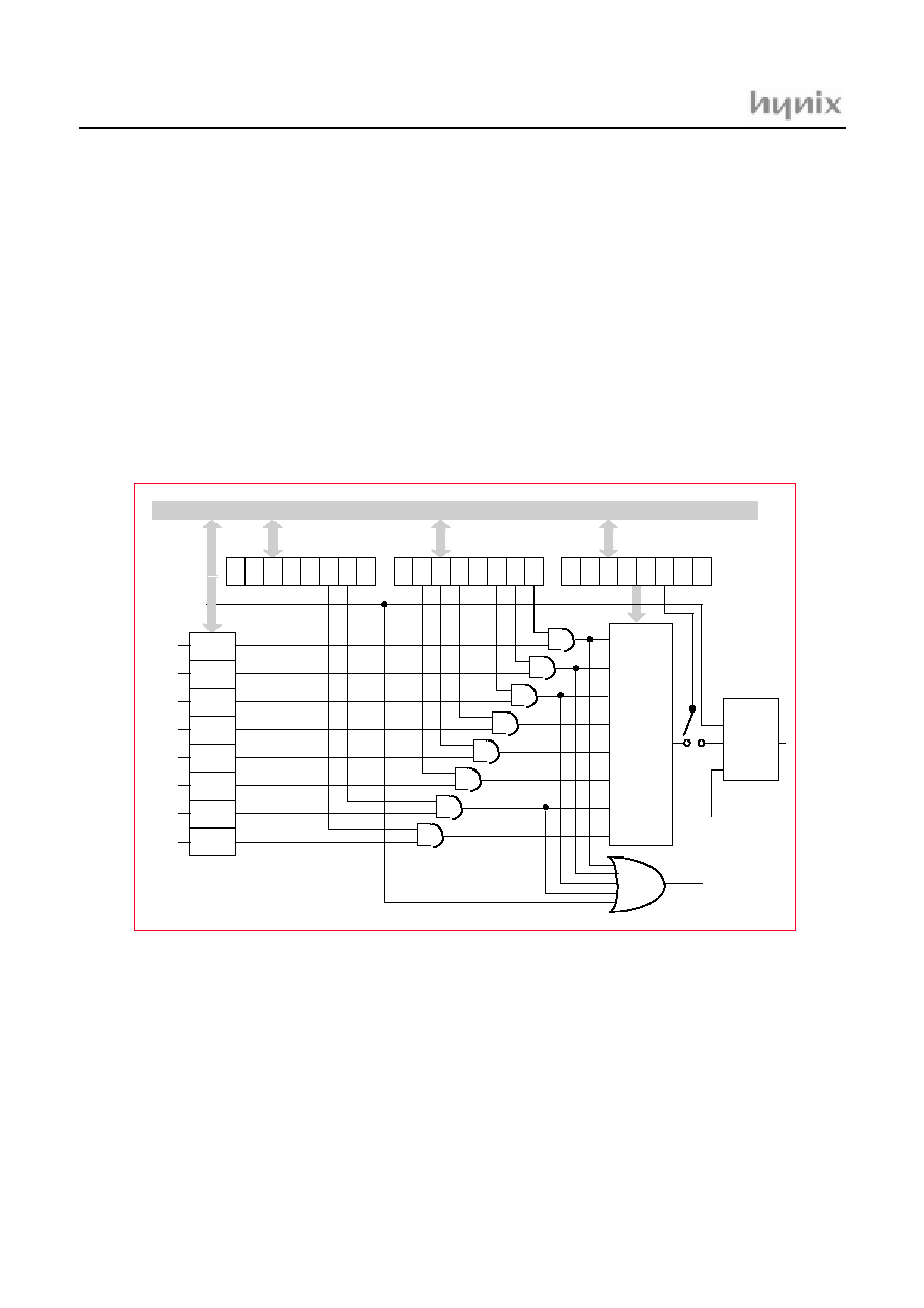
HMS87C5216
50
Sep. 2001 Ver 1.0
13. INTERRUPTS
The GMS81C5016/24/32 interrupt circuits consist of In-
terrupt Mode Register (MOD), Interrupt enable register
(IENH, IENL), Interrupt request flags of IRQH, IRQL,
Priority circuit and Master enable flag ("I" flag of PSW). 8
interrupt sources are provided. The configuration of inter-
rupt circuit is shown in Figure 13-1 .
The GMS81C5016/24/32 contains 8 interrupt sources; 3
externals and 5 internals. Nested interrupt services with
priority control is also possible. Software interrupt is non-
maskable interrupt, the others are all maskable interrupts.
- 8 interrupt source (2Ext, 3Timer, BIT, WDT and Key
Scan)
- 8 interrupt vector
- Nested interrupt control is possible
- Programmable interrupt mode
- Hardware accept mode
- Software selection accept mode
- Read and write of interrupt request flag are possible.
- In interrupt accept, request flag is automatically cleared.
Figure 13-1 Block Diagram of Interrupt
13.1 Interrupt priority and sources.
Each interrupt vector is independent and has its own prior-
ity. Software interrupt (BRK) is also available. Interrupt
source classification is shown in Table 13-1.
Internal Data Bus
KSCNR
INT1R
INT2R
T0R
T1R
T2R
WDTR
BITR
PRIORITY
CONTROL
IENL
IENH
IMOD
IRQ
KSCN
INT1
INT2
IFT0
IFT1
IFT2
IFWDT
IFBIT
INT.
VECTOR
ADDR.
BRK
Standby Mode Release
7
0
-
-
7
0
-
-
7
0
-
-
-
-
-
-
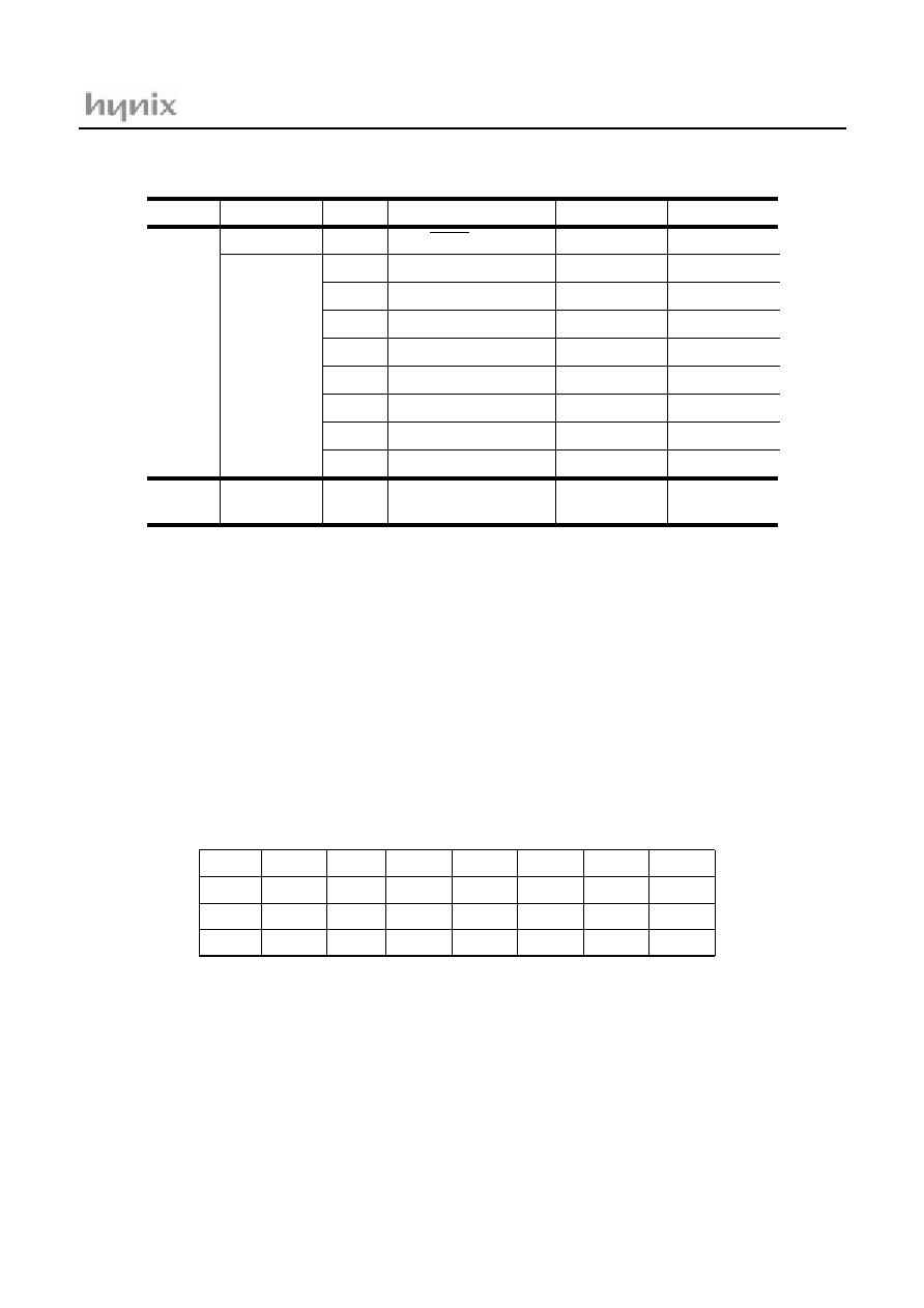
HMS87C5216
Sep. 2001 Ver 1.0
51
Table 13-1 Interrupt Priority & Source
13.2 INTERRUPT CONTROL REGISTER
I flag of PSW is a interrupt mask enable flag. When I flag
= ``0``, all interrupts become disable. When I flag = ``1``,
interrupts can be selectively enabled and disabled by con-
tents of corresponding Interrupt Enable Register. When in-
terrupt is occured, interrupt request flag is set, and
Interrupt request is detected at the edge of interrupt signal.
The accepted interrupt request flag is automatically cleared
during interrupt cycle process. The interrupt request flag
maintains ``1`` until the interrupt is accepted or is cleared
in program. In reset state, interrupt request flag register
(IRQH, IRQL) is cleared to ``0``. It is possible to read the
state of interrupt register and to mainpulate the contents of
register and to generate interrupt. (Refer to software inter-
rupt).
Mask
Priority
Interrupt Source
INT Vector High
INT Vector Low
Hardwar
e
Interrupt
INT2R (External Interrupt2)
non-maskable
maskable
-
0
1
2
3
4
5
6
7
-
INT1R (External Interrupt1)
-
WDTR (Watctdog Timer)
BITR (Basic Interval Timer)
RST (RESET pin)
KSCNR (Key Scan)
T0R (Timer0)
T1R (Timer1)
T2R (Timer2)
BRK instruction
FFFF
FFFE
FFFB
FFFA
FFF9
FFF8
FFF7
FFF6
FFF3
FFF2
FFF1
FFF0
FFEF
FFEE
FFE9
FFE8
FFE7
FFE6
FFDF
FFDE
-
WDTR
BITE
-
-
-
-
-
KSCNE
INT1E
INT2E
-
T0E
T1E
T2E
-
-
WDTR
BITE
-
-
-
-
-
KSCNE
INT1R
INT2R
-
T0R
T1R
T2R
-
IRQL
IRQH
R/W <00CFh>
R/W <00CDh>
R/W <00CEh>
R/W <00CCh>
IENH
IE N L
IENL : INTERRUPT ENABLE REGISTER LOW
IENH : INTERRUPT ENABLE REGISTER HIGH
IRQL : INTERRUPT REQUEST REGISTER LOW
IRQH : INTERRUPT REQUEST REGISTER HIGH
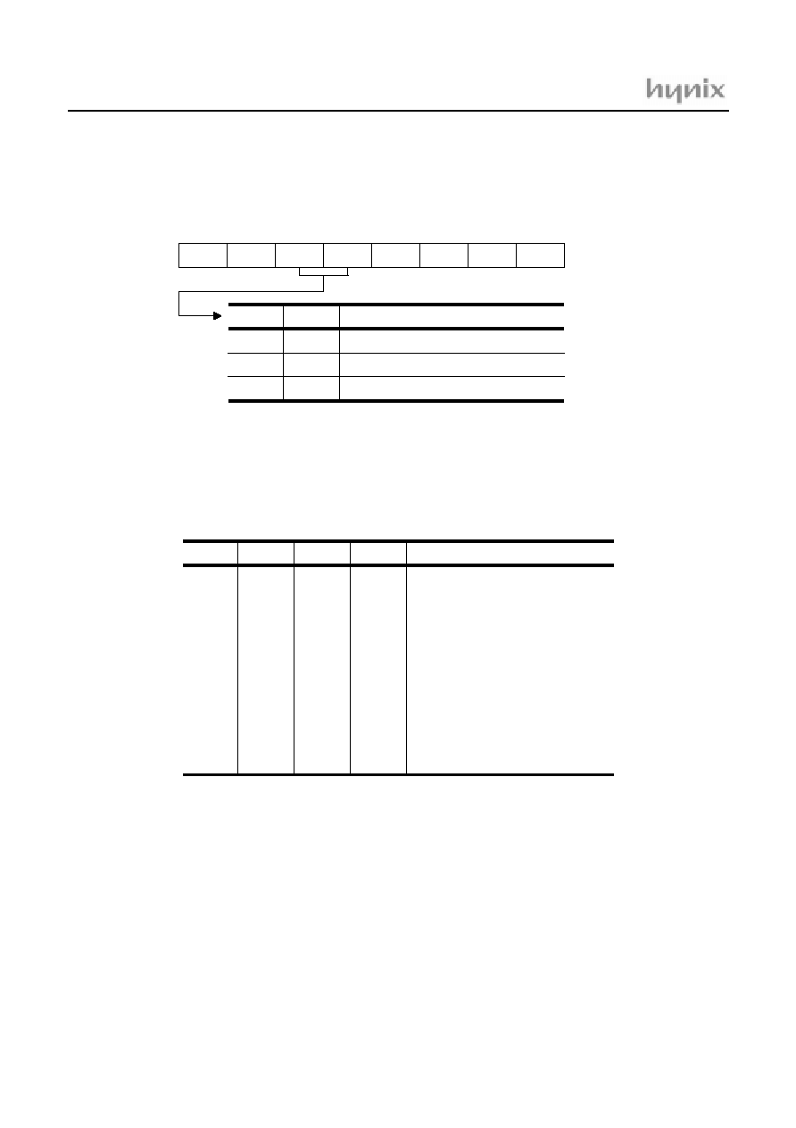
HMS87C5216
52
Sep. 2001 Ver 1.0
13.3 INTERRUPT ACCEPT MODE
The interrupt priority order is determined by bit (IM1,
IM0) of IMOD register.
(1) Selection of Interrupt by IP3-IP0
The condition allow for accepting interrupt is set state of
the interrupt mask enable flag and
the interrupt enable bit must be ``1``. In Reset state, these
IP3 - IP0 registers become all ``0``.
Table 13-2 Interrupt Selection by IP3 - IP0
0
-
-
IM1
IM0
IP3
IP2
IP1
IP0
7
R/W <00CA h>
IMOD
Interrupt Mode Register
IM1
IM0
0
0
0
1
1
*
Priority
fixed by hardware
changeable by IP3~ IP0
Interrupt is inhibited
Assigning by interrupt accept mode bit
0
0
0
0
0
0
0
1
1
1
1
1
0
0
0
1
1
1
1
0
0
0
0
1
0
1
1
0
0
1
1
0
0
1
1
0
1
0
1
0
1
0
1
0
1
0
1
0
KSCNR (Key Scan)
INT1R (External interrupt 1)
INT2R (External interrupt 2)
Reserved
T0R (Timer 0)
T1R (Timer 1)
T2R (Timer 2)
Reserved
Reserved
WDTR (Watch Dog Timer)
BITR (Basic Interval Timer)
Reserved
IP3
IP2
IP1
IP0
Selection Interrupt
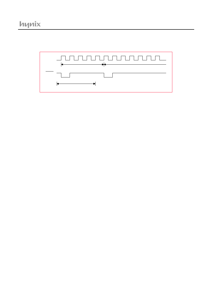
HMS87C5216
Sep. 2001 Ver 1.0
53
(2) Interrupt Timing
Figure 13-2 Interrupt Enable Accept Timing
*Interrupt Request sampling time
-Maximum 12 machine cycle (When execute DIV
instruction)
-Minimum 0 machine cycle
*Interrupt preprocess step is 8 machine cycle
*Interrupt overhead
-Maximum 1 + 12 + 8 = 21 machine cycle
-Minimum 1 + 0 + 8 = 9 machine cycle
(3) The valid timing after executing Interrupt control instructions
I flag is valid just after executing of EI/DI on the contrary.
Interrupt Enable register is valid one instruction after con-
trolling interrupt Enable Register.
13.4 INTERRUPT PROCESSING SEQUENCE
When an interrupt is accepted, the on-going process is
stopped and the interrupt service routine is executed. After
the interrupt service routine is completed it is necessary to
restore everything to the state before the interrupt oc-
cured.As soon as an interrupt is accepted, the content of the
program counter and PSW are savedin the stack area. At
the same time, the content of the vector address corre-
sponding to the accepted interrupt, which is in the interrupt
vector table, enters into the program counter and interrupt
service is executed. In order to execute the interrupt ser-
vice routine, it is necessary to write the jump addresses in
the vector table (FFE0 h ~ FFFF h) corresponding to each
interrupt
* Interrupt Processing Step
1) Store upper byte of Program Counter, SP <= SP
2) Store lower byte of Program Counter, SP <= SP - 1
3) Store Program Status Word, SP <= SP - 2
4) After resetting of I-flag, clear accepted Interrupt Re-
quest Flag. (Set B-flag for BRK Instruction)
5) Call Interrupt service routine
CLOCK
SYNC
A command before interrupt
interrupt process step
Interrupt Request Sampling
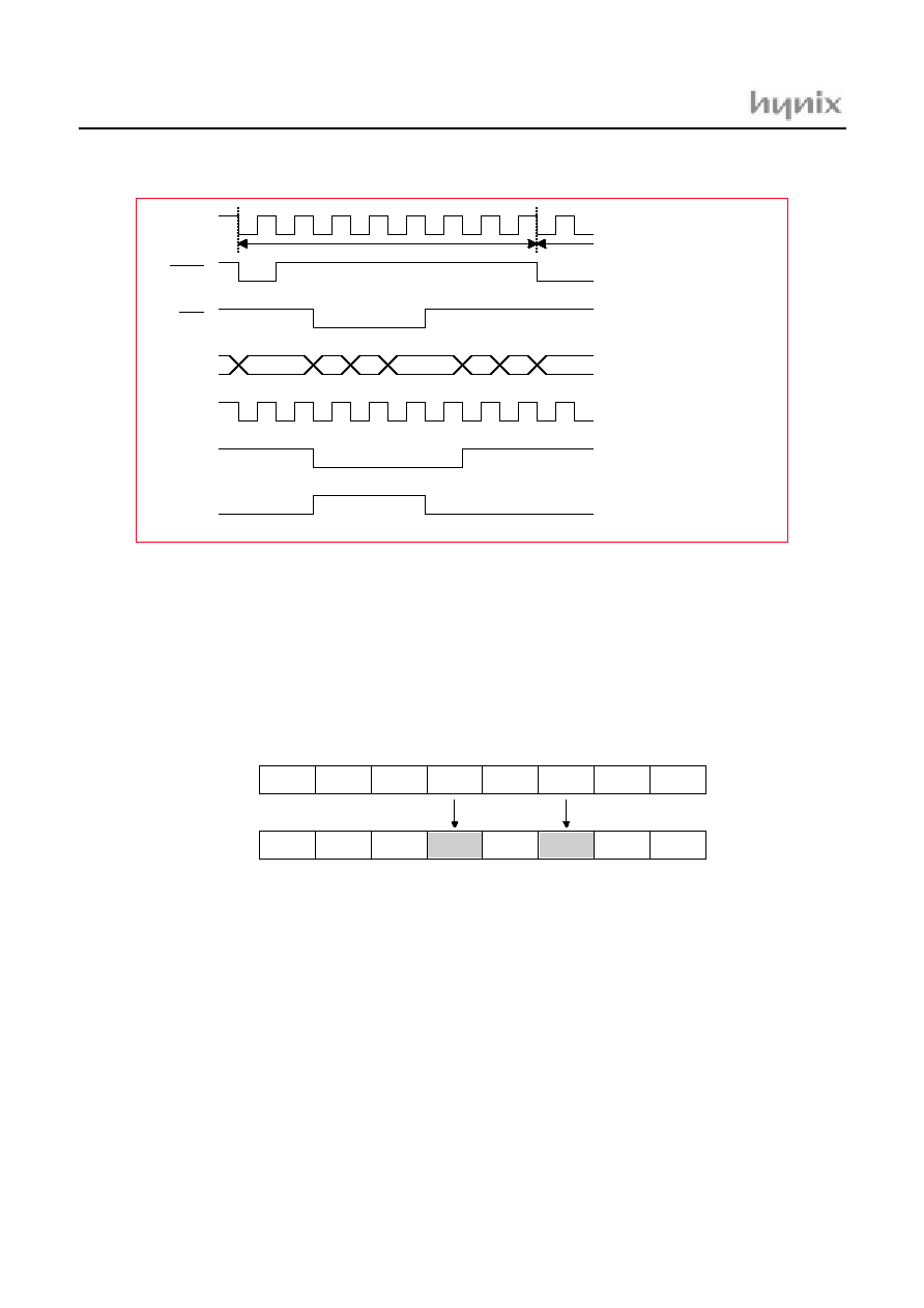
HMS87C5216
54
Sep. 2001 Ver 1.0
Figure 13-3 Interrupt Procesing Step Timing
13.5 SOFTWARE INTERRUPT (Interrupt by Break (BRK) Instruction)
S o f t w a r e i n t e r r u p t i s a v a i l a b l e j u s t b y w r i t i n g
``Break(BRK)`` instruction. The values of PC and PSW is
stacked by BRK instruction and then B flag of PSW is set
and I flag is reset.
Interrupt vector of BRK instruction is shared by vector of
Table Call (TCALL0). When both instruction of BRK and
TCALL0 are used, as shown in Figure 13-4 each process-
ing routine is judged by contents of B flag. There is no in-
struction to reset directly B flag.
*1 ISR
: Interrupt Service
Routine
*2 LVA
: Low Vector Address
*3 HVA
: High Vector Address
PC
Ê
OP
CODE
Interrupt Process Step
ISR
SP
SP-1
SP-2
LVA
HVA
new PC
*2
*3
*1
Ê
OP
CODE
Ê
PCH
Ê
PCL
Ê
PSW
Ê
``L``
vector
Ê
``H``
vector
clock
SYNC
R/W
internal
addr bus
internal
data bus
internal
READ
internal
WRITE
set
reset
(Right after BRK execution)
N
V
G
B
H
I
Z
C
PSW
Flag change by BRK execution
N
V
G
1
H
0
Z
C
PSW
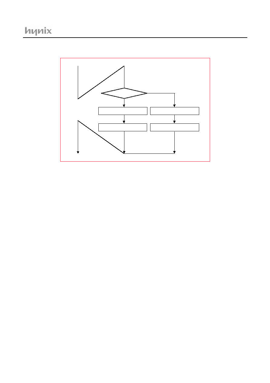
HMS87C5216
Sep. 2001 Ver 1.0
55
Figure 13-4 Execution of BRK or TCALL0
13.6 MULTIPLE INTERRUPT
If there is an interrupt, Interrupt Mask Enable Flag is auto-
matically cleared before entering the Interrupt Service
Routine. After then, no interrupt is accepted. If EI instruc-
tion is executed, interrupt mask enable bit becomes ``1``,
and each enable bit can accept interrupt request. When two
or more interrupts are generated simultaneously, the high-
est priority interrupt set by Interrupt Mode Register is ac-
cepted.
13.7 Key Scan Input Processing
(1) Standby Mode Release Register (SMRR)
Key Scan Interrupt is generated by detecting low or high
Input from each Input pin (R0, R1) is one of the sources
which release standby (SLEEP, STOP) mode. Key Scan
ports are all 16bit which are controlled by Standby Mode
Release Register (SMRR0, SMRR1). Key Input is consid-
ered as Interrupt, therefore, KSCNE bit of IEHN should be
set for correct interrupt executing, SLEEP mode and STOP
mode, the rest of executing is the same as that of external
Interrupt. Each SMRR Register bit is allowed for each port
(for Bit= ``0``, no Key Input, for Bit= ``1``, Key Input
available). At reset, SMRR becomes ``00 h``. So, there is
no Key Input source.
B flag
BRK INTERRUPT ROUTINE
TCALL0 ROUTINE
RETI
RET
BRK or
TCALL0
0
1
HMS87C5216
56
Sep. 2001 Ver 1.0
Figure 13-5 Key Scan Block
R00
R01
.
.
.
R07
R10
R11
.
.
.
R17
R0 port
Selection Logic
SMRR0
W <00DC h>
Internal
Key Scan
Interrupt
7
0
SMRR1
W <00DD h>
7
0
R0 port
Selection Logic
0
KR07
KR06
KR05
KR04
KR03
KR02
KR01
KR00
7
W <00DC h>
SMRR0
SMRR0 Register
0
KR17
KR16
KR15
KR14
KR13
KR12
KR11
KR10
7
W <00DD h>
SMRR1
SMRR1 Register
HMS87C5216
Sep. 2001 Ver 1.0
57
(2) Standby Release Level Control Register (SRLC)
Standby release level control register (SRLC) can select
the key scan input level ``L`` or ``H`` for standby release
by each bit pin (R0, R1). Standby release level control reg-
ister (SRLC) is write-only register and initialized as ``00
h`` in reset state.
SMRR0
KR07
Key Input Selection
0
1
no select
select
SMRR1
KR17
0
1
KR06
0
1
no select
select
KR16
0
1
KR05
0
1
no select
select
KR15
0
1
KR04
0
1
no select
select
KR14
0
1
KR03
0
1
no select
select
KR13
0
1
KR02
0
1
no select
select
KR12
0
1
KR01
0
1
no select
select
KR11
0
1
KR00
0
1
no select
select
KR10
0
1
0
KLR07
KLR06
KLR05
KLR04
KLR03
KLR02
KLR01
KLR00
7
W <00F6 h>
SRLC0
SRLC0 Register
0
KLR17
KLR16
KLR15
KLR14
KLR13
KLR12
KLR11
KLR10
7
W <00F7 h>
SRLC1
SRLC1 Register
HMS87C5216
58
Sep. 2001 Ver 1.0
SRLC0
KLR07
Key Input Level
0
1
Low
High
SRLC1
KLR17
0
1
KLR06
0
1
KLR16
0
1
KLR05
0
1
KLR15
0
1
KLR04
0
1
KLR14
0
1
KLR03
0
1
KLR13
0
1
KLR02
0
1
KLR12
0
1
KLR01
0
1
KLR11
0
1
KLR00
0
1
KLR10
0
1
Low
High
Low
High
Low
High
Low
High
Low
High
Low
High
Low
High
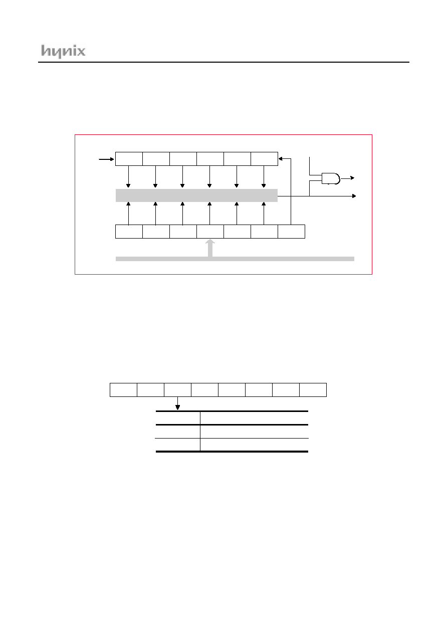
HMS87C5216
Sep. 2001 Ver 1.0
59
14. WATCH DOG TIMER
Watch Dog Timer (WDT) consists of 6-bit binary counter,
6-bit comparator, and Watch Dog Timer Register
(WDTR).
Figure 14-1 Block diagram of Watch Dog Timer
14.1 Control of WDT
Watch Dog Timer can be used 6-bit general Timer or spe-
cific Watch dog timer by setting
bit5 (WDTON) of Clock Control Register (CKCTLR).
By assigning bit6(WDTCL) of WDTR, 6-bit counter can
be cleared.
IFBIT
0
5
6BIT COMPARATOR
WDTR
W <00C8 h>
IF WDT
CLR
WDTON
To Reset circuit
Internal Data Bus
WDT0
WDT1
WDT2
WDT3
WDT4
WDT5
WDTR0
WDTR1
WDTR2
WDTR3
WDTR4
WDTR5
WDTCL
0
6
0
-
-
WDTON
ENPCK
BTCL
BTS2
BTS1
BTS0
7
W <00C7 h>
CKCTLR
Clock Control Register
WDTON
Watch Dog Timer Function Control
0
1
6-bit Timer
Watch Dog Timer
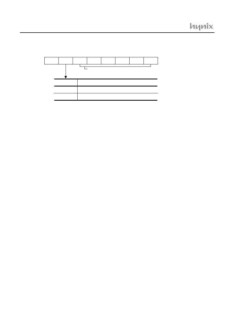
HMS87C5216
60
Sep. 2001 Ver 1.0
14.2 WDT Interrupt Interval
WDT Interrupt (IFWDT) interval is determined by the in-
terrupt IFBIT interval of Basic Interval Timer and the val-
ue of WDT Register.
-Interval of IFWDT = (IFBIT interval) * (WDTR value)
-Interval of IFWDT : 512 us * 1 = 512 us (MIN>)
-65,536us * 63 = 4,128,768 us (MAX>)
As IFBIT (Basic Interval Timer Interrupt Request) is used
for input clock of WDT, Input clock cycle is possible from
512 us to 65,536 us by BTS. (at fex = 4MHz)
*At Hardware reset time ,WDT starts automatically.
Therefore, the user must select the CKCTLR, WDTR be-
fore WDT overflow.
-Reset WDTR value = 0F h,15
-interval of WDT = 65,536 * 15 = 983040 us
(about 1second )
Determine Interval of IFWDT
Interval of IFWDT = Value of WDTR
ð
Interval of IFBIT
0
-
WDTCL
WDTR5
WDTR4
WDTR3
WDTR2
WDTR1
WDTR0
7
W <00C8 h>
WDTR
Watch DOG Timer Register
WDTCL
Watch Dog Timer Operation
0
1
free-run
Automatically cleared, after one machine cycle
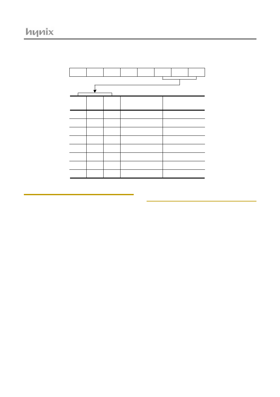
HMS87C5216
Sep. 2001 Ver 1.0
61
N o t e : W h e n W D T R R e g i s t e r v a l u e i s 6 3 ( 3 F h )
(Caution) : Do not use ``0`` for WDTR Register value.
Device come into the reset state by WDT
32,756 us
64,512 us
129,024 us
258,048 us
516,096 us
1,032,192 us
2,064,384 us
4,128,768 us
0
-
-
WDTON
ENPCK
BTCL
BTS2
BTS1
BTS0
7
W <00C7 h>
CKCTLR
Clock Control Register
BTS0
WDT Input clock
0
1
BTS1
0
0
BTS2
0
0
Max. Interval of WDT
Output (*note1)
0
1
0
1
1
0
0
0
1
1
0
1
0
1
1
1
1
1
512 us
1,024 us
2,048 us
4,096 us
8,192 us
16,384 us
32,768 us
65,536 us
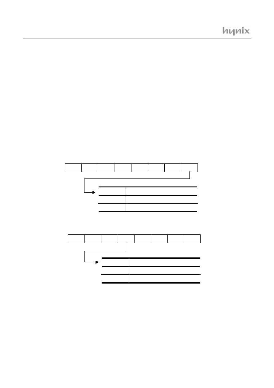
HMS87C5216
62
Sep. 2001 Ver 1.0
15. STANDBY FUNCTION
To save power consumption, there is STOP modes. In this
modes, the execution of program stops.
15.1 Sleep Mode
SLEEP mode can be entered by setting the bit of SLEEP
mode register (SLPM). In the mode, CPU clock stops but
oscillator keeps running. B.I.T and a part of peripheral
hardware execute, but prescalerÌs output which provide
clock to peripherals can be stopped by program. (Except,
PS10 canÌt stopped.) In SLEEP mode, more consuming
power can be saved by not using other peripheral hardware
except for B.I.T. By setting ENPCK (peripheral clock con-
trol bit) of CKCTLR (clock control register) to ``0``, pe-
ripheral hardware halted, and SLEEP mode is entered. To
release SLEEP mode by BITR (basic interval timer inter-
rupt), bit10 of prescaler should be selected as B.I.T input
clock before entering SLEEP mode. ``NOP`` instruction
should be follows setting of SLEEP mode for rising pre-
charge time of data bus line.
(ex) setting of SLEEP mode : set the bit of SLEEP
; mode register (SLPM)
NOP : NOP instruction
15.2 STOP MODE
STOP mode can be entered by STOP instruction during
program. In STOP mode, oscillator is stopped to make all
clocks stop, which leads to less power consumption. All
registers and RAM data are preserved. ``NOP`` instruction
should be follows STOP instruction for rising precharge
time of Data Bus line.
(ex) STOP : STOP instruction execution
NOP : NOP instruction
0
-
-
SLPM0
7
W <00F0 h>
SLPM
SLEEP MODE CONTROL Register
SLPM0
0
1
condition
sleep mode release
sleep mode
-
-
-
-
-
0
-
-
WDTON
ENPCK
BTCL
BTS2
BTS1
BTS0
7
W <00C8 h>
CKCTLR
Colck Control Register
ENCPK
0
1
Peripheral Clock
stopped
provided
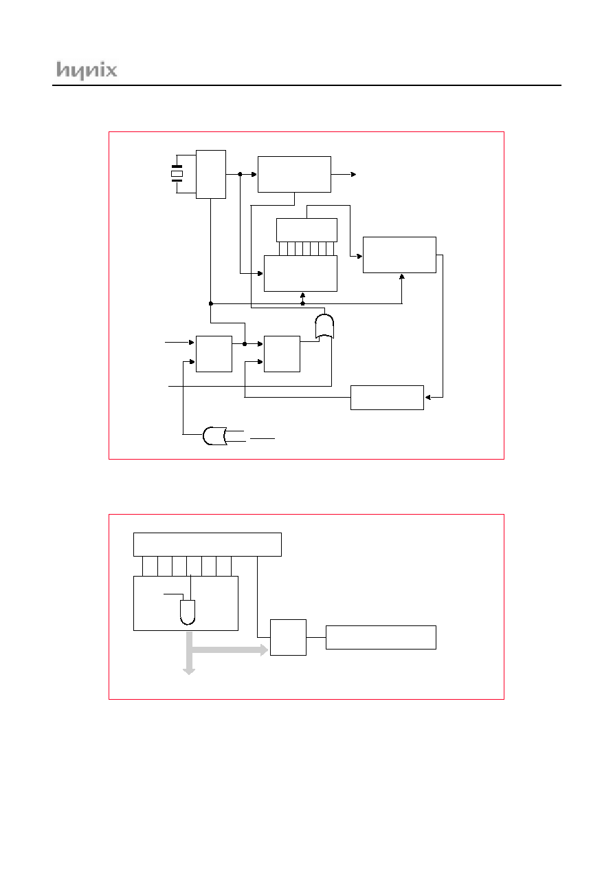
HMS87C5216
Sep. 2001 Ver 1.0
63
Figure 15-1 Block Diagram of Standby Circuit
Figure 15-2 ENPCK and Basic Interval Timer Clock
OSC.
Circuit
Clock Pulse GEN
CLR
MUX
Prescaler
CLR
S Q
R
S Q
R
Overflow Detection
Basic Interval Timer
CLR
CPU Clock
B.I.T 7
STOP
Release Signal From Interrupt Circuit
RESET
Control
Signal
Selector
Prescaler
ENPCK
Basic Interval Timer
PS10
Peripheral
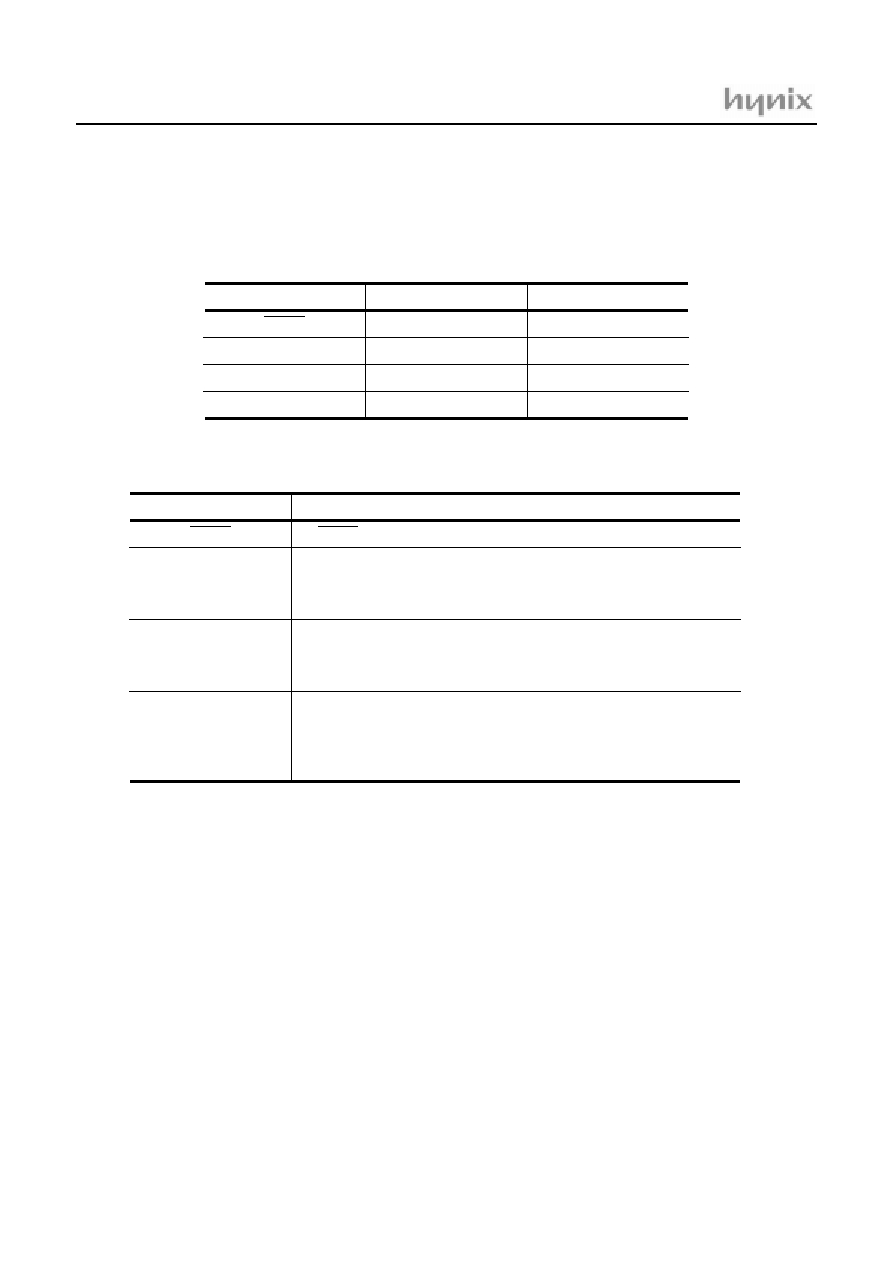
HMS87C5216
64
Sep. 2001 Ver 1.0
15.3 STANDBY MODE RELEASE
Release of STANDBY mode is executed by RESET input
and Interrupt signal. Register value is defined when Reset.
When there is a release signal of STOP mode (Interrupt,
RESET input), the instruction execution starts after stabi-
lization oscillation time is set by value of BTS2 ~ BTS0
and set ENPCK to ``1``.
Table 15-1 Standby Mode Register
Table 15-2 Standby Mode Release
Release Signal
KSCN (key input)
SLEEP
RESET
INT1 , INT2
B.I.T
STOP
O
O
O
O
O
O
O
X
Release Factor
KSCN
(key input)
Release Method
RESET
INT1
INT2
Basic Interval Timer
(IFBIT)
Standby mode is released by low input of selected pin by key scan Input
(SMRR0, SMRR1) In case of interrupt mask enable flag = ``0``,
program executes just after standby instruction,
if flag = ``1``, enters each interrupt service routine.
When external interrupt (INT1, INT2) enable flag is ``1``, standby mode is released
at the rising edge of each terminal. When Standby mode is released at interrupt.
Mask Enable flag = ``0``, program executes from the next instruction of standby
instruction. When ``1``, enters each interrupt service routine.
When B.I.T is executed only by bit10 of prescaler (PS10), SLEEP mode can be
release. Interrupt release SLEEP mode, when BIT interrupt enable flag is ``1``.
When standby mode is released at interrupt. Mask enable flag = ``0``,
program executes from the next instruction of SLEEP instruction.
When ``1``, enters each interrupt service routine.
By RESET Pin = Low level, Standby mode is release and system is initialized
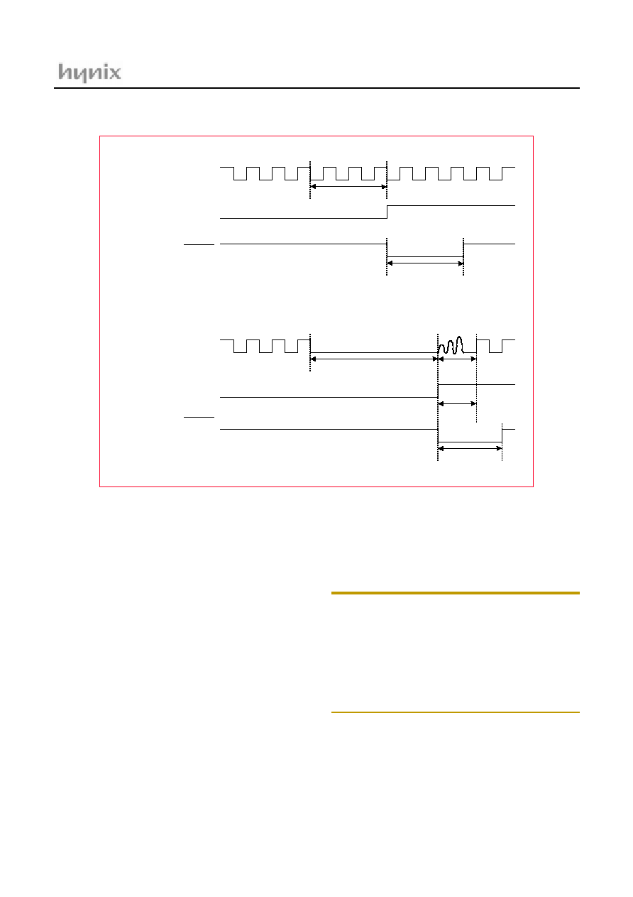
HMS87C5216
Sep. 2001 Ver 1.0
65
Figure 15-3 Release Timing of Standby Mode
15.4 RELEASE OPERATION OF STANDBY MODE
After standby mode is released, the operation begins ac-
cording to content of related interrupt register just before
standby mode start (Figure 15-4 )
(1) Interrupt Enable Flag(I) of PSW = ``0``
Release by only interrupt which interrupt enable flag =
``1``, and starts to execute from next to standby instruction
(SLEEP or STOP).
(2) Interrupt Enable Flag(I) of PSW = ``1``
Released by only interrupt which each interrupt enable flag
= ``1``, and jump to the relevant interrupt service routine.
Note: When STOP instruction is used, B.I.T should guar-
antee the stabilization oscillation time. Thus, just before en-
tering STOP mode, clock of bit10 (PS10) of prescaler is
selected or peripheral hardware clock control bit (ENPCK)
to ``1``, Therefore the clock necessary for stabilization os-
cillation time should be input into B.I.T. otherwise, standby
mode is released by reset signal. In case of interrupt re-
quest flag and interrupt enable flag are both ``1``, standby
mode is not entered.
STOP Mode
Stable
OSC. time
Program Setting Time by
CKCTLR
Longer than
stable OSC. Time
Xin
Longer than
2 machine cycle
SLEEP Mode
SLEEP command
[ SLEEP MODE ]
[ STOP MODE ]
release by interrupt
RESET
clock
release by interrupt
RESET
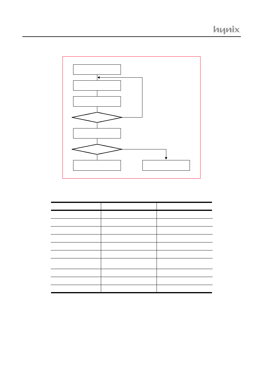
HMS87C5216
66
Sep. 2001 Ver 1.0
Figure 15-4 Standby Mode Release Flow
Table 15-3 Operation State in Standby Mode
STOP Command
Standby Mode
Interrupt Request GEN.
IE Flag
Standby Mode Release
PSW
IE Flag
Interrupt Service Routine
Standby Next Command
Execution
0
1
0
1
Internal circuit
STOP mode
SLEEP mode
Oscillator
Internal CPU clock
Register
RAM
I/O port
Prescaler
Basic Interval Timer
Watch Dog Timer
Timer
Address Bus, Data Bus
Active
Stop
Retained
Retained
Retained
Active
PS10 selected : Active
Others : Stop
Stop
Stop
Retained
Stop
Stop
Retained
Retained
Retained
Retained
Stop
Stop
Stop
Retained
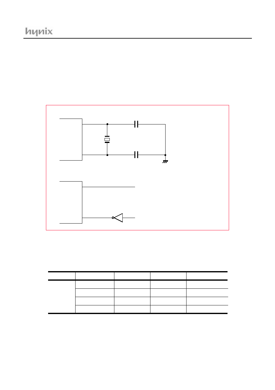
HMS87C5216
Sep. 2001 Ver 1.0
67
16. OSCILLATION CIRCUIT
Oscillation circuit is designed to be used either with a ce-
ramic resonator or crystal oscillator. Fig. 4.2-(a) shows
circuit diagrams using a crystal (or ceramic) oscillator. As
shown in the diagram, oscillation circuits can be construct-
ed by connecting a oscillator between Xout and Xin.
Clock from oscillation circuit makes CPU clock via clock
pulse generator, and then enters prescaler to make periph-
eral hardware clock. Alternately, the oscillator may be
driven from an external source as shown is Fig. 4.2.-(b). In
the Standby (STOP) mode, oscillatiion stop, Xout state
goes to ``HIigh``, Xin state goes to ``Low``, and built-in
feed back resistor is disabled.
Figure 16-1 Oscillator configurations
* Recommendable resonator
* MC type is building in load capacitior.CCR type is chip type.
Cout
Cin
Xin
Xout
(b) External clock input circuit
Xin
Xout
External clock
(a) External Crystal (Ceramic) oscillator circuit
Frequency
Resonator Maker
Part Name
Load Capacitor
Operating Voltage
4.0 MHz
CQ
ZTA4.00MG
Cin=Cout=30pF
2.2 ~ 4.0V
TDK
FCR4.0MC5
Cin=Cout=open
2.2 ~ 4.0V
TDK
FCR4.0M5
Cin=Cout=33pF
2.2 ~ 4.0V
TDK
CCR4.0MC3
2.2 ~ 4.0V
HMS87C5216
68
Sep. 2001 Ver 1.0
17. RESET FUNCTION
17.1 EXTERNAL RESET
The RESET pin should be held at low for at least 2machine
cycles with the power supply voltage within the operating
voltage range and must be connected 0.1uF capacitor for
stable system initialization. The RESET pin contains a
Schmitt trigger with an internal pull-up resistor.
Figure 17-1
17.2 POWER ON RESET
Power On Reset circuit automatically detects the rise of
power voltage (the rising time should be within 50ms) the
power voltage reaches a certain level, RESET terminal is
maintained at ∞ªL∞ª Level until a crystal ceramic oscillator
oscillates stably. After power applies and starting of oscil-
lation, this reset state is maintained for about oscillation
cycle of 219 (about 65.5ms : at 4MHz).The execution of
built-in Power On Reset circuit is as follows :
(1) Latch the pulse from Power On Detection Pulse Gener-
ator circuit, and reset Prescaler, B.I.T and B.I.T Overflow
detection circuit.
(2) Once B.I.T Overflow detection circuit is reset. Then,
Prescaler starts to count.
(3) Prescaler output is inputted into B.I.T and PS10 of
Prescaler output is automatically selected. If overflow of
B.I.T is detected, Overflow detection circuit is set.
(4) Reset circuit generates maximum period of reset pulse
from Prescaler and B.I.T.
Figure 17-2 Block Diagram of Power On Reset Circuit
RESET
0.1 uF Capacitor
RESET
Power On DET
Pulse GEN.
OSC.
CLR
Prescaler
CLR
Basic Interval
Tiemr
CLR
Basic Interval
Tiemr
XTAL
PS10
MSB
Internal Reset
VDD
VSS
0.1uF
Internal IC
HMS87C5216
Sep. 2001 Ver 1.0
69
Note: Notice ; When Power On Reset, oscillator stabiliza-
tion time doesn`t include OSC. Start time.
Figure 17-3 Oscillator stabilization diagram
Figure 17-4 Reset Timing by Diagram
17.3 Low Voltage Detection Mode
(1) Low voltage detection condition
An on board voltage comparator checks that VDD is at the
required level to ensure correct operation of the device. If
VDD is below a certain level, Low voltage detector forces
the device into low voltage detection mode.
(2) Low Voltage Detection Mode
There is no power consumption except stop current, stop
mode release function is disabled. All I/O port is config-
ured as input mode and Data memory is retained until volt-
age through external capacitor is worn out. In this mode,
all port can be selected with Pull-up resistor by Mask op-
tion. If there is no information on the Mask option sheet
,the default pull up option (all port connect to pull-up resis-
}kk
vzjU z{hy{ {ptpun
wylzjhsly jv|u{ z{hy{
RESET
ADDR. BUS
INTERNAL
DATA BUS
SP
SP-1
SP-2
FFFE
FFFF
NEW PC
FE
LSB
VECTOR
MSB
VECTOR
INTERNAL
RESET
HMS87C5216
70
Sep. 2001 Ver 1.0
tor ) is selected.
(3) Release of Low Voltage Detection Mode
Reset signal result from new battery(normally 3V) wakes
the low voltage detection mode and come into normal reset
state. It depends on user whether to execute RAM clear
routine or not.
Figure 17-5 Low Voltage vs Temperature
(4) SRAM BACK-UP after Low Voltage Detection.
0.0
0.2
0.4
0.6
0.8
1.0
1.2
1.4
1.6
1.8
2.0
2.2
2.4
0
◊
10
◊
20
◊
30
◊
40
◊
50
◊
60
◊
70
◊
{O◊P
s } O}P
2.6
2.8
3.0
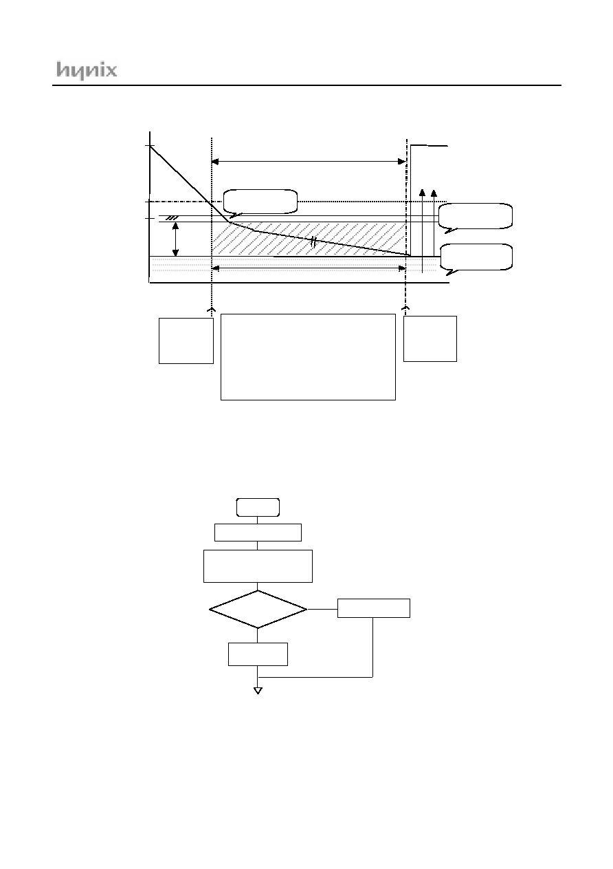
HMS87C5216
Sep. 2001 Ver 1.0
71
Figure 17-6 Low Voltage Detection and Protection
(5) S/W flow chart example after Reset using SRAM Back-up
Figure 17-7 S/W Flow Chart Example for SRAM Back-up
3.0V
1.8V(TYP)
( 20
◊P
* SRAM Data Backup
User
Removes
Batteries
User
Replace
Batteries
Interrupt :
disable
Stop release
: disable
All I/O port
: input Mode
Remout port
: Low Level
OSC :
STOP
All I/O port pull-up ON (Mask Option )
SRAM Data retention
* The operation after Low voltage detection
about hours depend on Vcc-Gnd Capacitor
0V
Low Voltage Detection
point
MCU OPR.
Voltage
Power On Reset
( SRAM unstable )
Power On Reset
( SRAM retention)
0.7V(V
RET
)
RESET
Stack Pointer initialize
SRAM DATA IS VALID?
Check the SRAM value
(RAM Pattern, Check sum..)
N
Y
Clear All Ram area
Use saved SRAM
value

HMS87C5216
72
Sep. 2001 Ver 1.0
17.4 Low Voltage Indicator Register (LVIR)
Low Voltage Indication Register (LVIR) is read only Reg-
ister. It is useful to display the consumption of Batteries.
If VDD power level is below a cirtain level which is higher
than low voltage detection level ( refer to Figure 17-6 ) ,
The bit of LVIR register could be set according to the VDD
level sequentially. The VDD dection levels for Indication
are two , that is , Bit1 and Bit0 of LVIR Register. The de-
tection level of Bit0 is higer than Bit1.
-
-
-
-
-
-
LVIR1
LVIR0
<00EF h>
LVIR
bit
7
6
5
4
3
2
1
0
initial value
-
-
-
-
-
0
0
R / W
-
-
-
-
-
R
R
-
-
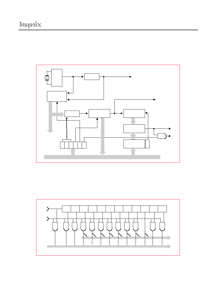
HMS87C5216
Sep. 2001 Ver 1.0
73
18. CLOCK GENERATOR
Clock generating circuit consists of Clock Pulse Generator
(C.P.G), Prescaler, Basic Interval Timer (B.I.T) and Watch
Dog Timer. The clock applied to the Xin pin divided by
two is used as the internal system clock.
Figure 18-1 Block Diagram of Clock Generator
Prescaler consists of 12-bit binary counter. The clock sup-
plied from oscillation circuit is input to prescaler (fex).
The divided output from each bit of prescaler is provided
to peripheral hardware.
Figure 18-2 Block diagram of Prescaler
9
PRESCALER
C.P.G
MUX
WDT (6)
COMPARATOR
Internal Data Bus
0
1
2
3
4
0
5
6
6
WDTON
To Reset
Circuit
IFWDT
WDTCL
IFBIT
5
0
7
0
fcpu
fex
PS1
ENPCK
Peripheral
CKCTLR
BTCL
3
8
OSC
Circuit
B.I.T (8)
6
WDTR
Internal System Clock
5
B.I.T
Peripheral
PS0
PS1
PS2
PS3
PS4
PS5
PS6
PS7
PS8
PS9
PS10 PS11
PS12
fex
ENPCK
fcpu
PS1
PS2
PS3
PS4
PS5
PS6
PS7
PS8
PS9
PS10
PS11
PS12
HMS87C5216
74
Sep. 2001 Ver 1.0
Table 18-1 ps output perio Basic Interval Timer
The HMS87C5216 and GMS81C1408 has one 8-bit Basic
Interval Timer that is free-run, can not stop. Block diagram
is shown in Figure 18-3 .The 8-bit Basic interval timer reg-
ister (BITR) is increased every internal count pulse which
is divided by prescaler. Since prescaler has divided ratio by
8 to 1024, the count rate is 1/8 to 1/1024 of the oscillator
frequency. As the count overflows from FF
H
to 00
H
, this
overflow causes to generate the Basic interval timer inter-
rupt. The BITF is interrupt request flag of Basic interval
timer.
When write "1" to bit BTCL of CKCTLR, BITR register is
cleared to "0" and restart to count-up. The bit BTCL be-
comes "0" after one machine cycle by hardware.
If the STOP instruction executed after writing "1" to bit
WAKEUP of CKCTLR, it goes into the wake-up timer
mode. In this mode, all of the block is halted except the os-
cillator, prescaler (only fxin
˜
2048) and Timer0.
If the STOP instruction executed after writing "1" to bit
RCWDT of CKCTLR, it goes into the internal RC oscillat-
ed watchdog timer mode. In this mode, all of the block is
halted except the internal RC oscillator, Basic Interval
Timer and Watchdog Timer. More detail informations are
explained in Power Saving Function. The bit WDTON de-
cides Watchdog Timer or the normal 7-bit timer
Note: All control bits of Basic interval timer are in CKCTLR
register which is located at same address of BITR
(address EC
H
). Address EC
H
is read as BITR, writ-
ten to CKCTLR. Therefore, the CKCTLR can not be
accessed by bit manipulation instruction.
.
Figure 18-3 Block Diagram of Basic Interval Timer
fex (MHz)
4 MHz
2 MHz
frequency
period
frequency
period
ps 0
ps 1
ps 2
ps 3
ps 4
ps 5
ps 6
ps 7
ps 8
ps 9
ps 10
ps 11
ps 12
4 MHz
2 MHz
1 MHz
500 KHz
250 KHz
125 KHz
62.5 KHz
31.25 KHz
15.63 KHz
7.183 KHz
3.906 KHz
1.953 KHz
0.976 KHz
250 ns
500 ns
1 us
2 us
4 us
8 us
16 us
32 us
64 us
128 us
256 us
512 us
1024 us
2 MHz
1 MHz
500 KHz
250 KHz
125 KHz
62.5 KHz
31.25 KHz
15.63 KHz
7.183 KHz
3.906 KHz
1.953 KHz
0.976 KHz
0.488 KHz
500 ns
1 us
2 us
4 us
8 us
16 us
32 us
64 us
128 us
256 us
512 us
1024 us
2048 us
˜
8
˜
16
˜
128
˜
256
˜
512
˜
1024
˜
32
˜
64
0
1
MUX
8
3
fxin
BITR (8BIT)
BITIF
BTS[2:0]
RCWDT
Internal RC OSC
Basic Interval Timer
Interrupt
BTCL
Clear
To Watchdog Timer
HMS87C5216
Sep. 2001 Ver 1.0
75
Figure 18-4 CKCTLR: Clock Control Register
Clock Control Register
CKCTLR
ADDRESS : ECH
RESET VALUE : -0010111
-
WAKEUP
RCWDT
WDTON
BTCL
BTS2
BTS1
BTS0
Basic Interval Timer Clock Selection
000 : fxin
˜
8
001 : fxin
˜
16
100 : fxin
˜
128
101 : fxin
˜
256
110 : fxin
˜
512
111 : fxin
˜
1024
010 : fxin
˜
32
011 : fxin
˜
64
Symbol
Function Description
WAKEUP
1 : Enables Wake-up Timer
0 : Disables Wake-up Timer
RCWDT
1 : Enables Internal RC Watchdog Timer
0 : Disables Internal RC Watchdog Time
WDTON
1 : Enables Watchdog Timer
0 : Operates as a 7-bit Timer
BTCL
1 : BITR is cleared and BTCL becomes "0" automatically
after one machine cycle, and BITR continue to count-up
Bit Manipulation Not Available
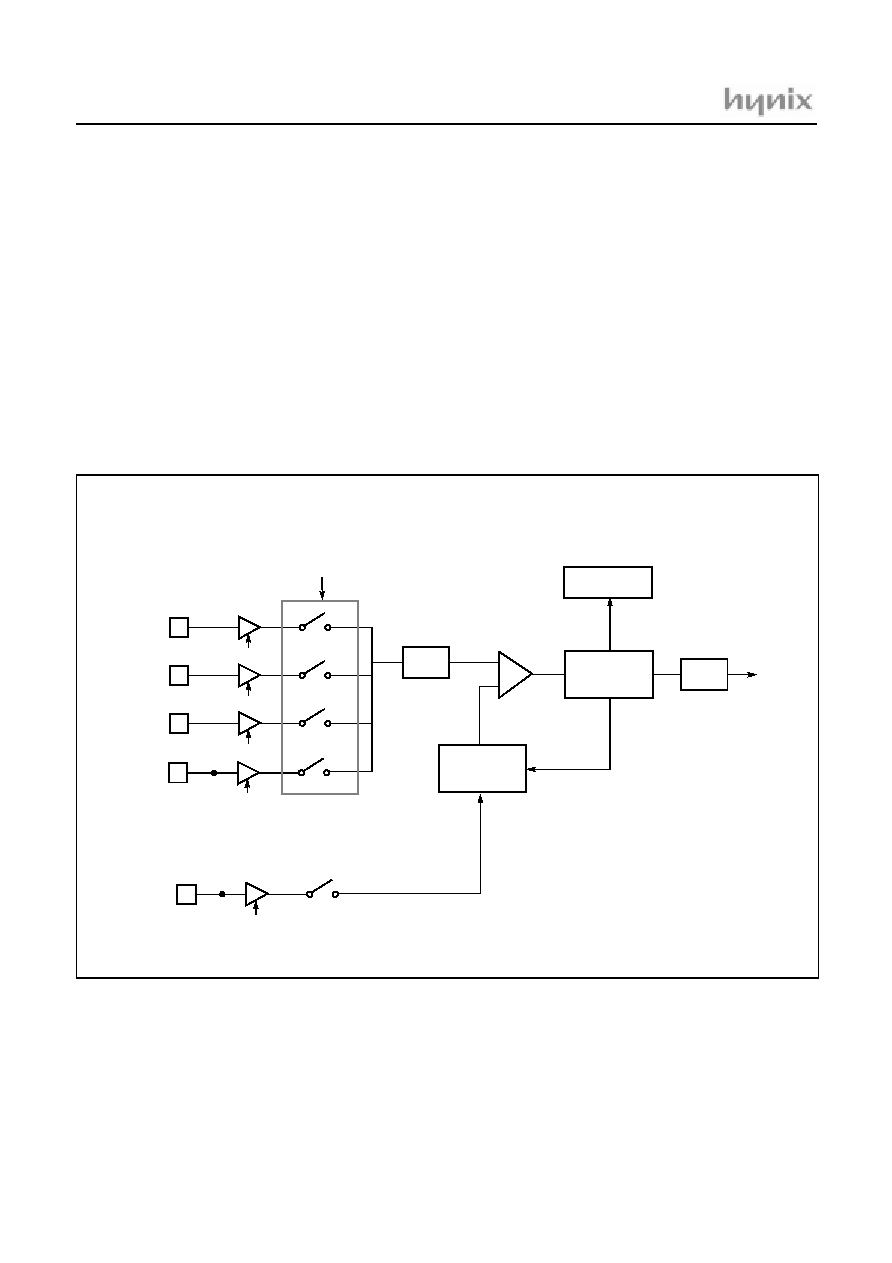
HMS87C5216
76
Sep. 2001 Ver 1.0
19. ANALOG TO DIGITAL CONVERTER
The analog-to-digital converter (A/D) allows conversion
of an analog input signal to a corresponding 8-bit digital
value. The A/D module has eight analog inputs, which are
multiplexed into one sample and hold. The output of the
sample and hold is the input into the converter, which gen-
erates the result via successive approximation.
The analog reference voltage is V
DD
. The A/D module has
two registers which are the control register ADMR and A/
D result register ADDR. The ADMR register, shown in
Figure 19-2 , controls the operation of the A/D converter
module. The port pins can be configure as analog inputs or
digital I/O.
To use analog inputs, each port is assigned analog input
port by setting the bit ANSEL[7:0] in RAFUNC register.
And selected the corresponding channel to be converted by
setting ADS[2:0].
The processing of conversion is start when the start bit
ADST is set to "1". After one cycle, it is cleared by hard-
ware. The register ADCR contains the results of the A/D
conversion. When the conversion is completed, the result
is loaded into the ADCR, the A/D conversion status bit
ADSF is set to "1", and the A/D interrupt flag ADIF is set.
The block diagram of the A/D module is shown in Figure
19-1 . The A/D status bit ADSF is set automatically when
A/D conversion is completed, cleared when A/D conver-
sion is in process. The conversion time takes maximum 30
uS (at fxin=4 MHz).
Figure 19-1 A/D Converter Block Diagram
R1[4]/AN0
ADEN
R1[5]/AN1
ADEN
R1[6]/AN2
ADEN
R1[7]/AN3
ADEN
00
01
10
11
S/H
Successive
Approximation
Circuit
A D IF
Resistor
Ladder
Circuit
ADDR(8-bit)
Sample & Hold
A/D Interrupt
ADDRESS : EDH
RESET VALUE : Undefined
A/D Result Register
AVDD
ADEN
ADAN[1:0]
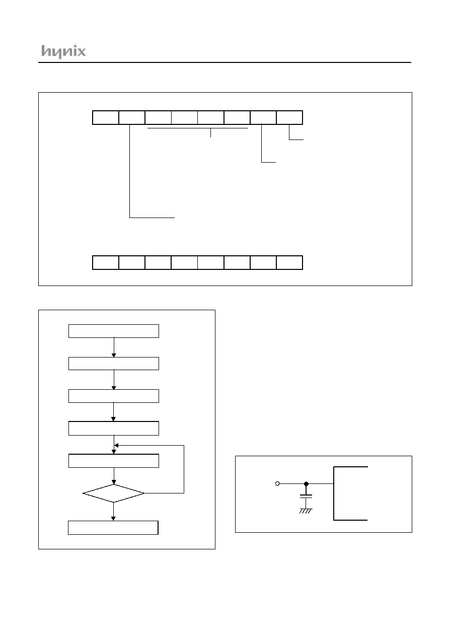
HMS87C5216
Sep. 2001 Ver 1.0
77
Figure 19-2 A/D Converter Registers
Figure 19-3 A/D Converter Operation Flow
A/D Converter Cautions
(1) Input range of AN0 to AN3
The input voltage of AN0 to AN3 should be within the
specification range. In particular, if a voltage above
VDD
or below Vss is input (even if within the absolute maximum rat-
ing range), the conversion value for that channel can not be inde-
terminate. The conversion values of the other channels may also
be affected.
(2) Noise countermeasures
In order to maintain 8-bit resolution, attention must be paid to
noise on pins VDD and AN0 to AN3. Since the effect increases
in proportion to the output impedance of the analog input source,
it is recommended that a capacitor be connected externally as
shown in Figure 19-4 in order to reduce noise.
Figure 19-4 Analog Input Pin Connecting Capacitor
(3) Pins AN0/R1[4] and AN1/R1[5] to AN3/R1[7]
ADMR
ADDRESS : F4H
RESET VALUE : --000001
-
ANEN
ADAN3
ADAN2
ADAN1
ADAN0
ADST
ADF
Analog Channel Select
A/D Status bit
0 : A/D Conversion is in process
1 : A/D Conversion is completed
A/D Start bit
1 : A/D Conversion is started
After 1 cycle, cleared to "0"
0 : Bit force to zero
0000 : Channel 0 (R1[4]/AN0)
0001 : Channel 1 (R1[5]/AN1)
0010 : Channel 2 (R1[6]/AN2)
0011 : Channel 3 (R1[7]/AN3)
A/D Enable bit
1 : A/D Conversion is enable
0 : A/D Converter module shut off
and consumes no operation current
A/D Control Register
ADCR
ADDRESS : F5H
RESET VALUE : Undefined
ADCR7
ADCR6
ADCR5
ADCR4
ADCR3
ADCR2
ADCR1
ADCR0
A/D Result Data Register
ENABLE A/D CONVERTER
A/D START (ADST = 1)
NOP
ADSF = 1
A/D INPUT CHANNEL SELECT
ANALOG REFERENCE SELECT
READ ADCR
YES
NO
AN0~AN3
100~1000pF
Analog
Input

HMS87C5216
78
Sep. 2001 Ver 1.0
The analog input pins AN0 to AN3 also function as input/
output port (PORT R1 ) pins. When A/D conversion is per-
formed with any of pins AN0 to AN3 selected, be sure not
to execute a PORT input instruction while conversion is in
progress, as this may reduce the conversion resolution.
Also, if digital pulses are applied to a pin adjacent to the
pin in the process of A/D conversion, the expected A/D
conversion value may not be obtainable due to coupling
noise. Therefore, avoid applying pulses to pins adjacent to
the pin undergoing A/D conversion.