/home/web/htmldatasheet/RUSSIAN/html/hynix/173032
HMS91C7134
November.2001 ver1.0 1
HMS91C7134
CMOS SINGLE-CHIP 8-BIT MICROCONTROLLER
FOR MONITOR
1. OVERVIEW
1.1 Description
The HMS9xC7134 is a single-chip microcontroller of the 80C51 family, which is dedicated for monitor application. It is particularly suit-
able for multi-sync computer monitor controller. This contains DDC interfaces to the PC host, sync-detector and sync-processor for auto-
sync application, ADC, static PWM, dynamic PWM and I
2
C bus interface for control of the video and deflection functions of the monitor.
1.2 Features
· 80C51 core
· 32K bytes of ROM for HMS91C7134
(32K bytes of EPROM for HMS97C7134)
· 256 bytes of RAM and 256 bytes of XRAM for
DDC operation
· Uses an external crystal of 12.0 MHz
· One DDC compliant interface :
- Fully supports DDC1 with dedicated hardware
- DDC2B, DDC2AB and DDC2B+ compliant dedi-
cated hardware based on an I
2
C bus interface
- RAM buffer with programmable size, 128 bytes
or 256 bytes, which can be used for DDC opera-
tion or shared as system RAM
· On-chip sync processor
- HSYNC frequency with 12-bit resolution
- VSYNC frequency with 12-bit resolution
- HSYNC and VSYNC polarity
- HSYNC and VSYNC presence detection
- Composite sync separation
- Free running sync. generation
- Clamping pulse output
- Pattern generation
- Separate input for a SOG signal
- Missing pulse insertion option
- HSYNC/ VSYNC change interrupt
· One multi-master/slave I2C interface (up to
400K bit/s) for control of other system IC's
· Eight 8-bit Static PWM outputs for digital con-
trol applications
· Two 8-bit Dynamic PWM outputs for various
waveform generation
· One 8-bit ADC with 4 input channels
· LED driver port ; two port lines with
15 mA drive capability
· One 8-bit port only for I/O function
· 24 derivative I/O ports configurable for alterna-
tive functions
· Watchdog timer (524ms max.)
· On-chip low VDD voltage detect and reset
(reset period: 524ms)
· Operating temperature : 0
to 70
· Special idle and power-down modes with low
power consumption
· Single power supply : 4.5V to 5.5V
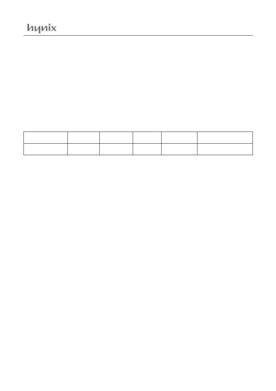
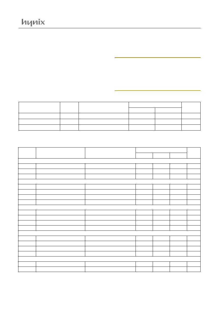
Device name
ROM Size
RAM
Size
I/O
OTP
Package
HMS91C7134
32K bytes
Mask ROM
512 bytes
30(42DIP)
32(42SDIP)
HMS97C7134
40DIP(HMS91C7134),
42SDIP(HMS91C7134K)
HMS91C7134
2
November.2001 ver1.0
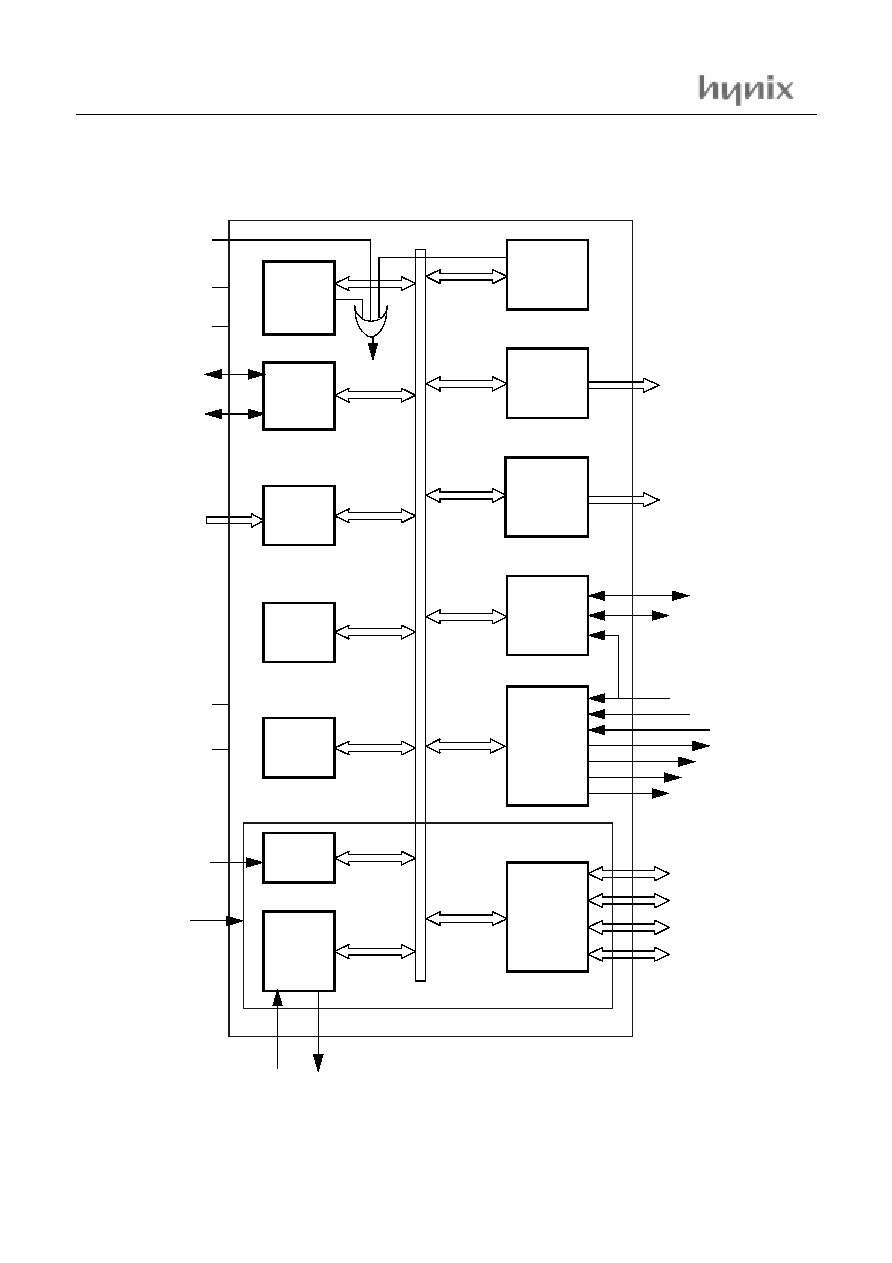
2. BLOCK DIAGRAM
VD
D2
V
S
S
2
RE
S
E
T
S
DA2
S
C
L
2
A
C
H
[
3:
0]
V
DD1
V
SS1
IN
T
0
XT
AL
1
XT
AL
2
DP
W
M
0
t
o
DP
W
M
1
PW
M
0
t
o
PW
M
7
SD
A
1
SC
L
1
P
0
P
1
P
2
P
3
P
A
T
OUT
C
L
A
M
P
HS
YNC
o
u
t
VS
YNC
o
u
t
VS
YNC
i
n
HS
YNC
i
n
S
OGi
n
T
h
r
ee 1
6
-
B
i
t
T
i
m
e
r
s
(
T0,
T1,
T
2
)
CP
U
P
r
ogr
a
m
Me
m
o
r
y
(
64K
B
)
D
a
t
a
Me
m
o
r
y
(
64K
B
)
8-
B
i
t
ADC
I
2
C-
Bu
s
S
e
ri
a
l
I/
O
Wa
t
c
h
D
o
g
T
i
m
e
r
P
a
r
a
lle
l
I/
O
P
o
rt
s
&
Ex
t
e
r
n
a
l
B
u
s
S
y
n
c
.
D
e
te
c
tio
n
&
S
ync
.
P
r
oc
e
s
s
DDC
In
t
e
rfa
c
e
8x8-
B
i
t
S
t
a
tic
PW
M
2x8-
B
i
t
D
yna
m
i
c
PW
M
L
o
w
V
o
lta
g
e
R
e
s
e
t
80
C
5
1 c
o
r
e
HMS91C7134
November.2001 ver1.0 3
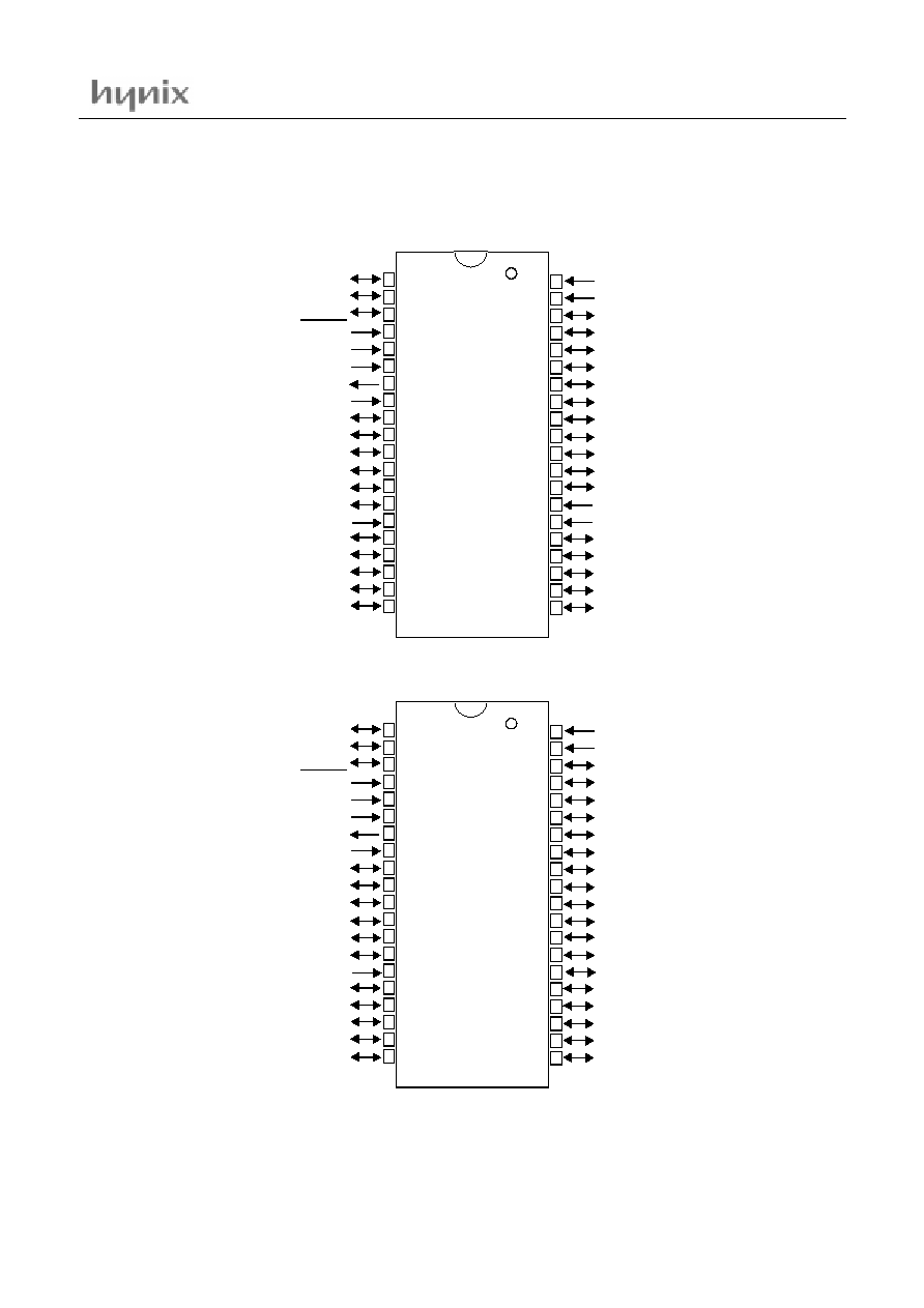
3. PIN ASSIGNMENT
3.1 40PDIP pinning
Vsync-IN
Hsync-IN
PWM1* /P2.3
PWM2* /P2.4
PWM3* /P2.5
PWM4* /P2.6
PWM5* /P2.7
Hsync-OUT /P3.2
Vsync-OUT /P3.3
PWM6* /INT1 /P3.4
CLAMP/PWM /P3.5
PADOUT /P3.6
SOG /P3.7
V
DD2
V
SS2
SCL1** /P1.0
SDA1** /P1.1
ACH0 /P1.2
ACH1 /P1.3
ACH2 /P1.4
PWM0* /P2.2
DPWM0* /P2.1
DPWM0* /P2.0
RESET
V
DD1
V
SS1
XTAL2
XTAL1
SDA2** /P1.7
SCL2** /P1.6
P0.7**
P0.6**
P0.5**
P0.4**
INT0/VPP
P0.3**
P0.2**
P0.1**
P0.0**
ACH3 /P1.5
40
39
38
37
36
35
34
33
32
31
30
29
28
27
26
25
24
23
22
21
1
2
3
4
5
6
7
8
9
10
11
12
13
14
15
16
17
18
19
20
H
M
S
9
x
C
71
32
* : Open-drain option
** : Open-drain type pin
40DIP
(Top View)
Vsync-IN
Hsync-IN
PWM1* /P2.3
PWM2* /P2.4
PWM3* /P2.5
PWM4* /P2.6
PWM5* /P2.7
Hsync-OUT /P3.2
Vsync-OUT /P3.3
PWM6* /INT1 /P3.4/CLAMP
PWM /P3.5
PADOUT /P3.6
SOG /P3.7
P3.0
P3.1
SCL1** /P1.0
SDA1** /P1.1
ACH0 /P1.2
ACH1 /P1.3
ACH2 /P1.4
PWM0* /P2.2
DPWM0* /P2.1
DPWM0* /P2.0
RESET
V
DD1
V
SS1
XTAL2
XTAL1
SDA2** /P1.7
SCL2** /P1.6
P0.7**
P0.6**
P0.5**
P0.4**
INT0/VPP
P0.3**
P0.2**
P0.1**
P0.0**
ACH3 /P1.5
40
39
38
37
36
35
34
33
32
31
30
29
28
27
26
25
24
23
22
21
1
2
3
4
5
6
7
8
9
10
11
12
13
14
15
16
17
18
19
20
H
M
S
9
xC
71
34
* : Open-drain option
** : Open-drain type pin
40DIP
(Top View)
HMS91C7134
4
November.2001 ver1.0
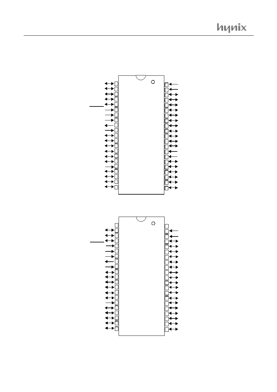
3.2 42SDIP pinning
Vsync-IN
Hsync-IN
PWM1* /P2.3
PWM2* /P2.4
PWM3* /P2.5
PWM4* /P2.6
PWM5* /P2.7
Hsync-OUT /P3.2
Vsync-OUT /P3.3
PWM6* /INT1 /P3.4
CLAMP/PWM /P3.5
PADOUT /P3.6
SOG /P3.7
V
DD2
V
SS2
SCL1** /P1.0
SDA1** /P1.1
ACH0 /P1.2
ACH1 /P1.3
ACH2 /P1.4
ACH3 /P1.5
PWM0* /P2.2
DPWM0* /P2.1
DPWM0* /P2.0
P3.1
P3.0
RESET
V
DD1
V
SS1
XTAL2
XTAL1
SDA2** /P1.7
SCL2** /P1.6
P0.7**
P0.6**
P0.5**
P0.4**
INT0/VPP
P0.3**
P0.2**
P0.1**
P0.0**
42
41
40
39
38
37
36
35
34
33
32
31
30
29
28
27
26
25
24
23
22
1
2
3
4
5
6
7
8
9
10
11
12
13
14
15
16
17
18
19
20
21
H
M
S
9
x
C
71
32
K
* : Open-drain option
** : Open-drain type pin
42SDIP
(Top View)
NC
Vsync-IN
Hsync-IN
PWM1* /P2.3
PWM2* /P2.4
PWM3* /P2.5
PWM4* /P2.6
PWM5* /P2.7
Hsync-OUT /P3.2
Vsync-OUT /P3.3
PWM6* /INT1 /P3.4/CLAMP
PWM7* /P3.5
PADOUT /P3.6
SOG /P3.7
P3.0
P3.1
SCL1** /P1.0
SDA1** /P1.1
ACH0 /P1.2
ACH1 /P1.3
ACH2 /P1.4
NC
PWM0* /P2.2
DPWM0* /P2.1
DPWM0* /P2.0
RESET
V
DD1
V
SS1
XTAL2
XTAL1
SDA2** /P1.7
SCL2** /P1.6
P0.7**
P0.6**
P0.5**
P0.4**
INT0/VPP
P0.3**
P0.2**
P0.1**
P0.0**
ACH3 /P1.5
42
41
40
39
38
37
36
35
34
33
32
31
30
29
28
27
26
25
24
23
22
1
2
3
4
5
6
7
8
9
10
11
12
13
14
15
16
17
18
19
20
21
H
M
S
9
x
C
71
34
K
* : Open-drain option
** : Open-drain type pin
42SDIP
(Top View)
HMS91C7134
November.2001 ver1.0 5
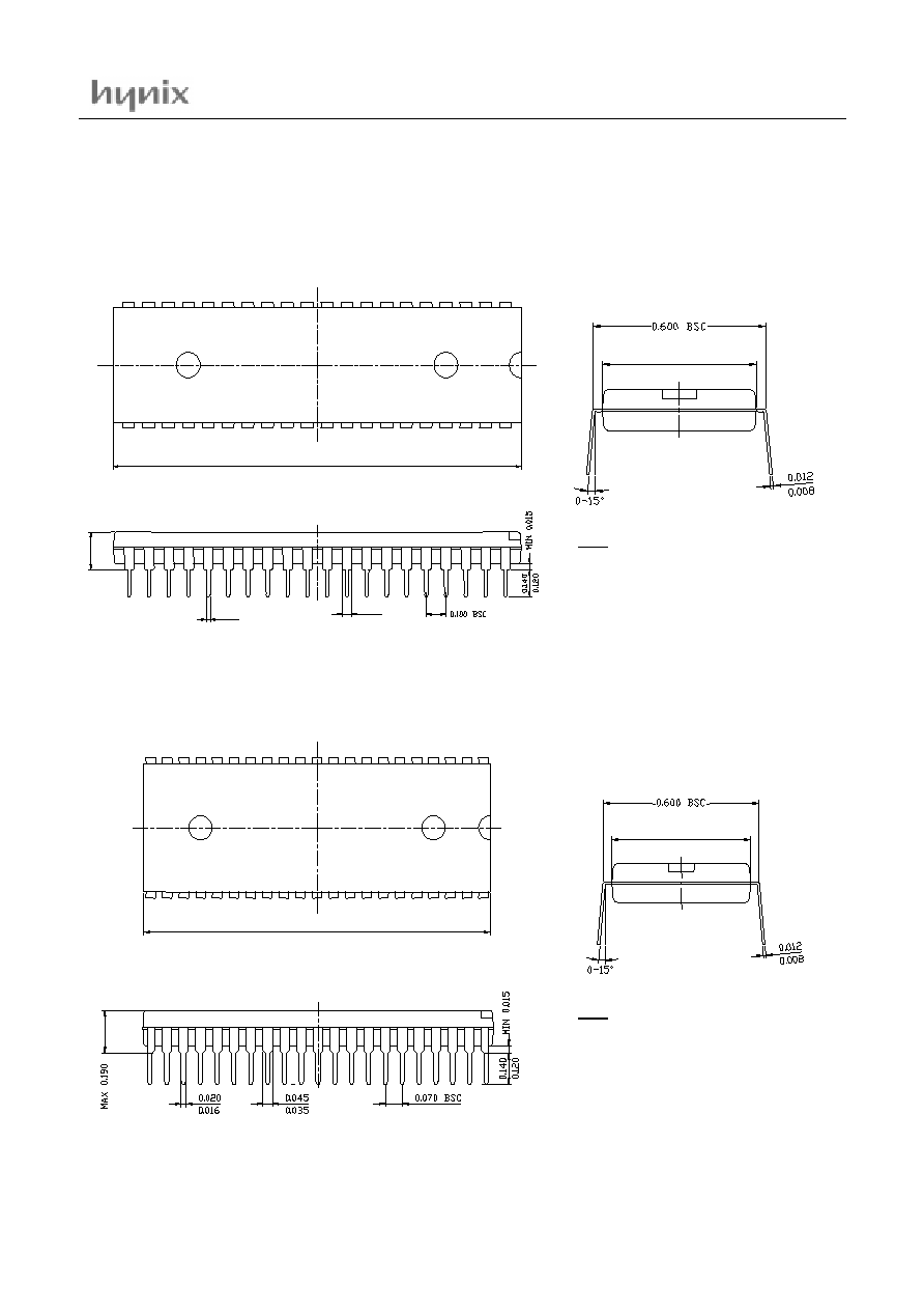
4. PACKAGE DIMENSIONS
4.1 40 PDIP
4.2 42 SDIP
2.075
2.045
M
AX 0.
20
0
0.022
0.015
0.065
0.045
NOTE
1. DIMENSIONS DO NOT INCLUDE MOLD
FLASH AND DAMBAR PROTRUSION.
ALLOWABLE MOLD FLASH IS 0.010 INCH.
2. CONTROLLING DIMENSION : INCH.
0.550
0.530
1.470
1.450
NOTE
1. DIMENSIONS DO NOT INCLUDE MOLD
FLASH AND DAMBAR PROTRUSION.
ALLOWABLE MOLD FLASH IS 0.010 INCH.
2. CONTROLLING DIMENSION : INCH.
0.550
0.530

HMS91C7134
6
November.2001 ver1.0
5. PIN FUNCTION
V
DD1
: Supply voltage (Digital).
V
SS1
: Circuit ground (Digital).
V
DD2
: Supply voltage (Analog).
V
SS2
: Circuit ground (Analog).
RESET: Reset the MCU.
XTAL1: Input to the inverting oscillator amplifier and input to
the internal main clock operating circuit.
XTAL2: Output from the inverting oscillator amplifier.
HSYNC
IN
: Horizontal sync input
VSYNC
IN
: Vertical sync input
INT0/V
PP
: External Interrupt input. Programming supply volt-
age(during OTP programming)
PORT:
The HMS9xC7134 has four 8-bit ports (Port0, Port1, Port2,
and Port3). Port0 - Port3 are the same as in the 80C51, with
the exception of the additional functions of Port1, Port2 and
Port3. Each has latch, SFR P0~P3' output driver and input
buffer.
P0.0~P0.7: P0 is an 8-bit CMOS bidirectional I/O port. P0 pins
have not pull-up resister and open-drain port. It has the capability
of drive LED. However, while the alternative function is per-
formed, the port type will remain the same. In case of application
to extention of external memory, P0 outputted Write/Read byte
and lower byte of external memory address. Therefore when it is
used as normal I/O port, P0 is open-drain driver and when it used
as bus port, P0 is 3-state driver.
P1.0~P1.7: P1 is an 8-bit CMOS bidirectional I/O port. Because
P1 pins have pull-up resister, it is called as Quasi-Bidirectional
port.
P2.0~P2.7: P2 is an 8-bit CMOS bidirectional I/O port. Because
P2 pins have pull-up resister, it is called as Quasi-Bidirectional
port. .
P3.0~P3.7: P3 is an 8-bit CMOS bidirectional I/O port. Because
P3 pins have pull-up resister, it is called as Quasi-Bidirectional
port.
Port pin
Alternate function
P0.0
P0.1
P0.2
P0.3
P0.4
P0.5
P0.6
P0.7
No (Only for I/O function)
No (Only for I/O function)
No (Only for I/O function)
No (Only for I/O function)
No (Only for I/O function)
No (Only for I/O function)
No (Only for I/O function)
No (Only for I/O function)
Port pin
Alternate function
P1.0
P1.1
P1.2
P1.3
P1.4
P1.5
P1.6
P1.7
SCL1 (DDC-SCL)
SDA1 (DDC-SDA)
ACH0
ACH1
ACH2
ACH3
SCL2 (I
2
C-SCL)
SDA2 (I
2
C-SDA)
Port pin
Alternate function
P2.0
P2.1
P2.2
P2.3
P2.4
P2.5
P2.6
P2.7
DPWM0*
DPWM1*
PWM0*
PWM1*
PWM2*
PWM3*
PWM4*
PWM5*
Port pin
Alternate function
P3.0
P3.1
P3.2
P3.3
P3.4
P3.5
P3.6
P3.7
Reserved
Reserved
HSYNC
OUT
VSYNC
OUT
PWM6*
CLAMP/PWM7
PATOUT
SOG
HMS91C7134
November.2001 ver1.0 7
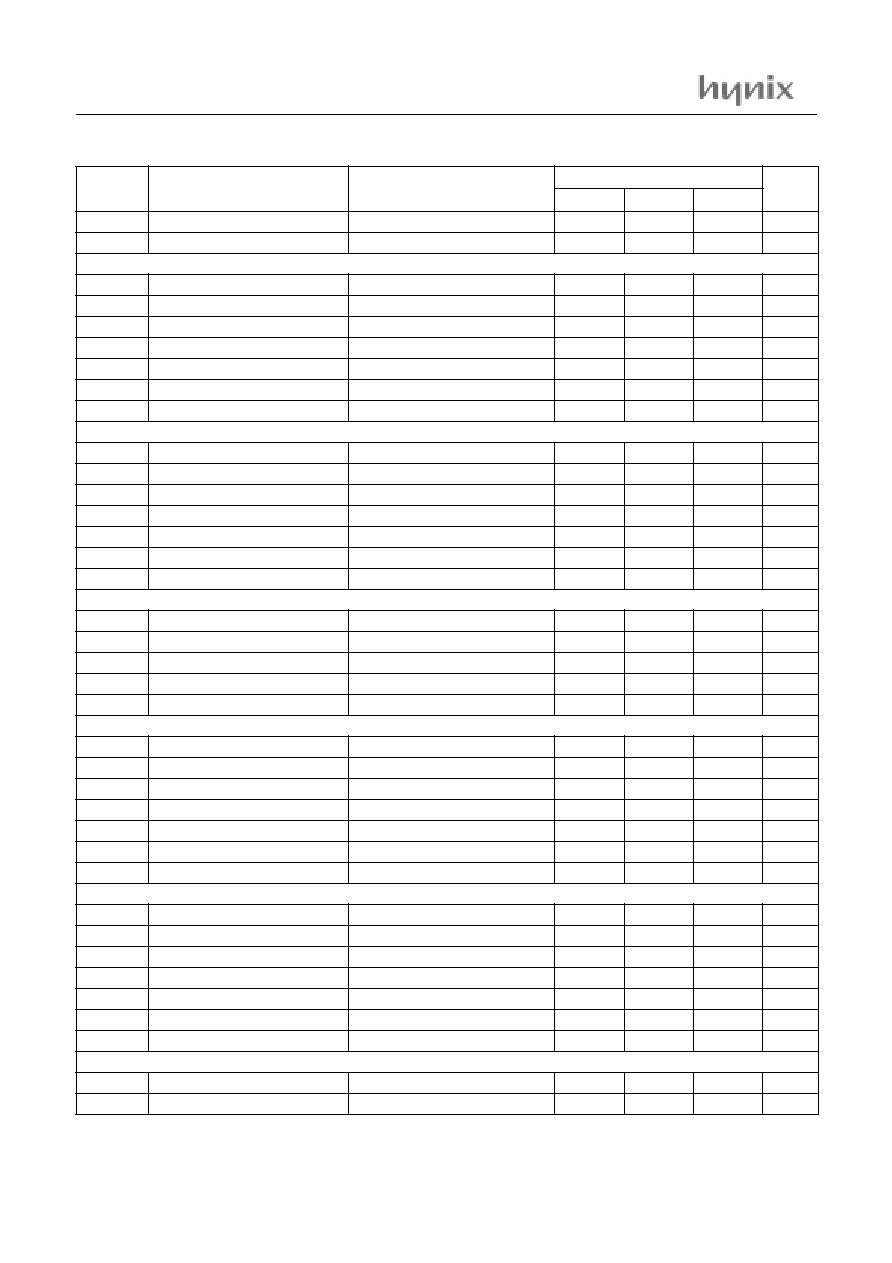
5.1 40DIP Pin Description
PIN NAME
(Alternate)
Pin
No.
In/Out
(Alter-
nate)
Function
Basic
Alternate
PWM0 /P2.2
1
I/O
General I/O port P2.2
8-bit Pulse Width Modulation output0
DPWM0 /P2.1
2
I/O
General I/O port P2.1
8-bit Dynamic Pulse Width Modulation output0
DPWM0 /P2.0
3
I/O
General I/O port P2.0
8-bit Dynamic Pulse Width Modulation output1
RESET
4
I
Reset input
V
DD1
5
-
Power supply1(+5V)
V
SS1
6
-
Ground1
XTAL2
7
O
Oscillator output pin for system clock
XTAL1
8
I
Oscillator input pin for system clock
SDA2 /P1.7
9
I/O
General I/O port P1.7
I
2
C serial data I/O port
SCL2 /P1.6
10
I/O
General I/O port P1.6
I
2
C serial clock I/O port
P0.7
11
I/O
General I/O port P0.7; adapted for LED driver
P0.6
12
I/O
General I/O port P1.6; adapted for LED driver
P0.5
13
I/O
General I/O port P0.5
P0.4
14
I/O
General I/O port P0.4
INT0 /V
PP
15
I
External interrupt input0; Programming supply voltage (during OTP programming)
P0.3
16
I/O
General I/O port P0.3
P0.2
17
I/O
General I/O port P0.2
P0.1
18
I/O
General I/O port P0.1
P0.0
19
I/O
General I/O port P0.0
ACH3 /P1.5
20
I/O
General I/O port P1.5
ADC channel3 input
ACH2 /P1.4
21
I/O
General I/O port P1.4
ADC channel2 input
ACH0 /P1.3
22
I/O
General I/O port P1.3
ADC channel1 input
ACH0 /P1.2
23
I/O
General I/O port P1.2
ADC channel0 input
SDA1 /P1.1
24
I/O
General I/O port P1.1
I
2
C serial data I/O port for DDC interface
SCL1 /P1.0
25
I/O
General I/O port P1.0
I
2
C serial clock I/O port for DDC interface
P3.1
26
I/O
General I/O port P3.1
P3.0
27
I/O
General I/O port P3.0
SOGin /P3.7
28
I/O
General I/O port P3.7
Sync on Green input
PATOUT /P3.7
29
I/O
General I/O port P3.6
Pattern out
PWM7 /P3.5 /
PROG
30
I/O
General output only port P3.5
Program pulse input(during OTP
programming)
8-bit Pulse Width Modulation output7
PWM6 /P3.4 /
INT1/CLAMP
31
I/O
General I/O port P3.4
8-bit Pulse Width Modulation output6; External
interrupt input1; Clamp out
VSYNCout /P3.3
32
I/O
General I/O port P3.3
Vertical sync output
HSYNCout /P3.2
33
I/O
General I/O port P3.2
Horizontal sync output
PWM5 /P2.7
34
I/O
General I/O port P2.7
8-bit Pulse Width Modulation output5
PWM4 /P2.6
35
I/O
General I/O port P2.6
8-bit Pulse Width Modulation output4
PWM3 /P2.5
36
I/O
General I/O port P2.5
8-bit Pulse Width Modulation output3
PWM2 /P2.4
37
I/O
General I/O port P2.4
8-bit Pulse Width Modulation output2
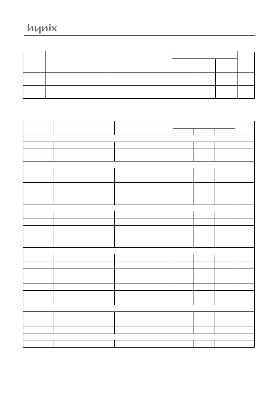
Table 5-1 Port Function Description(40DIP)

HMS91C7134
8
November.2001 ver1.0
5.2 42SDIP Pin Description
The 42SDIP type pin description is the same as The 40DIP type pin description except for adding two pins(P3.1, P3.0) to it
between pin no.4 and 5.
PWM1 /P2.3
38
I/O
General I/O port P2.3
8-bit Pulse Width Modulation output1
HSYNCin
39
I
Horizontal sync input
VSYNCin
40
I
Vertical sync input
PIN NAME
(Alternate)
Pin
No.
In/Out
(Alter-
nate)
Function
Basic
Alternate
Table 5-1 Port Function Description(40DIP)
HMS91C7134
November.2001 ver1.0 9
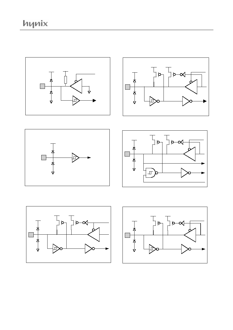
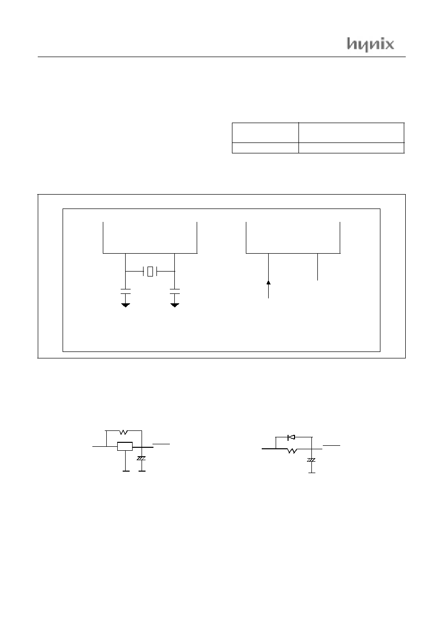
6. PORT STRUCTURES
P0.0 - P0.7
P1.2 - P1.5
P3.2, P3.3, P3.5
P3.7
data
CMOS
15mA
oen
data
CMOS
TTL
adc_enb
oen
data
adc_in
CMOS
internal reset
data
TTL
oen
data
TTL
P1.0, P1.1, P1.6, P1.7, P2, P3.0, P3.1, P3.4, P3.6
HSYNCIN, VSYNCIN
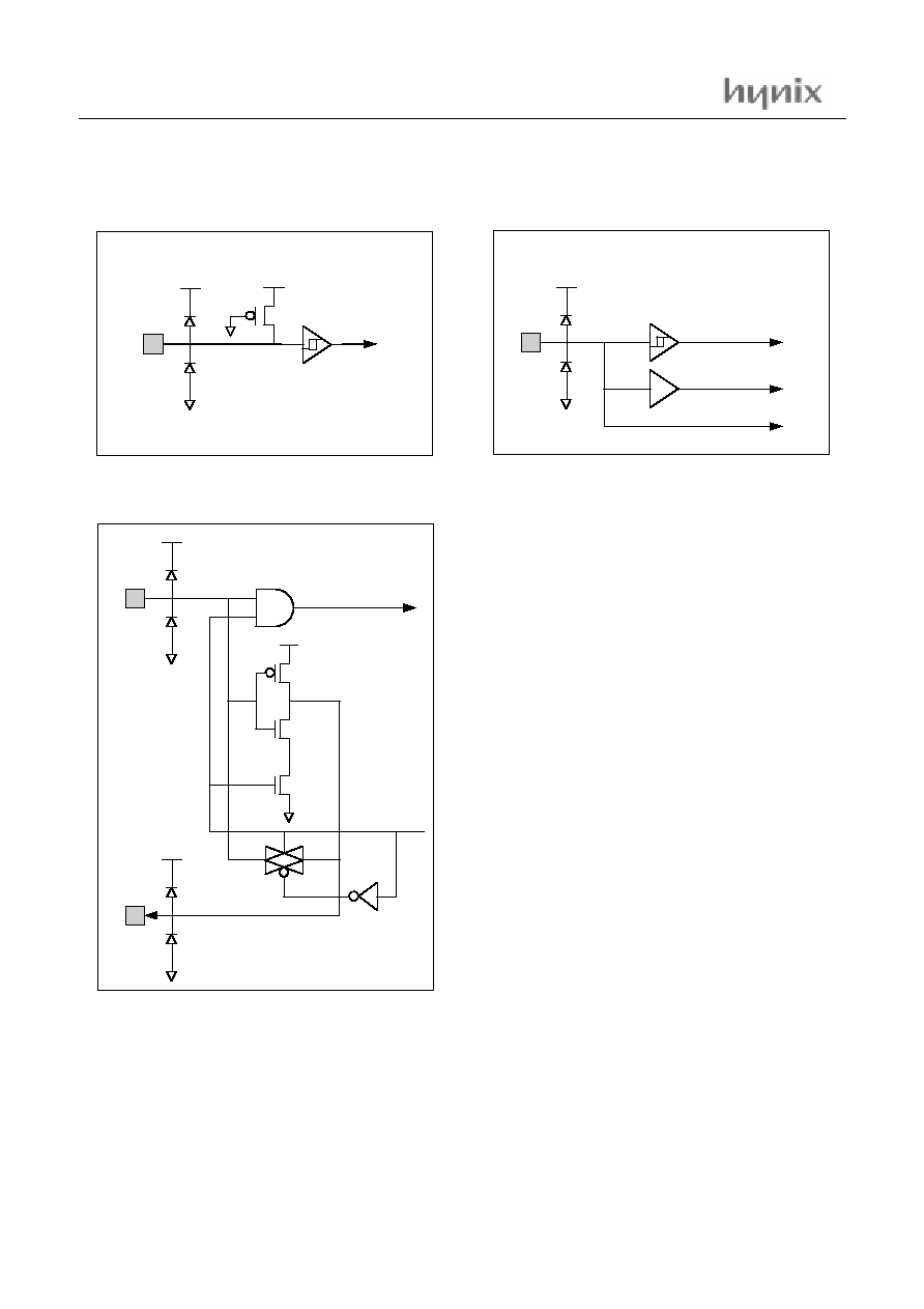
HMS91C7134
10
November.2001 ver1.0
INT0/VPP
XTAL1, XTAL2
CMOS
H
TTL
VPP detector
VPP
pdb
RESET
HMS91C7134
November.2001 ver1.0
11
7. ELECTRICAL CHARACTERISTICS
7.1 Absolute Maximum Ratings
Supply voltage......................................................-0.5 to +6.5 V
Input voltage...............................................-0.5 to VDD+0.5 V
Operating Temperature ............................................0 to +70
°
C
Storage Temperature .......................................... -65 to +150
°
C
Poweer Dissipation .................................................... TBD mW
Note: Stresses above those listed under "Absolute Maxi-
mum Ratings" may cause permanent damage to the de-
vice. This is a stress rating only and functional operation of
the device at any other conditions above those indicated in
the operational sections of this specification is not implied.
Exposure to absolute maximum rating conditions for ex-
tended periods may affect device reliability.
7.2 Recommended Operating Conditions
7.3 DC Electrical Characteristics
(T
A
= 0~70
°
C, V
DD
=4.5~5.5V, V
SS
=0V )
,
Parameter
Symbol
Condition
Specifications
Unit
Min.
Max.
Supply Voltage
V
DD
f
XIN
=12MHz
4.5
5.5
V
Operating Frequency
f
XIN
V
DD
=4.5~5.5V
10
16
MHz
Operating Temperature
T
OPR
-
0
70
°
C
Symbol
Parameter
Condition
Specifications
Unit
Min.
Typ.
Max.
SUPPLY
VDD
power supply voltage
-
4.5
5.0
5.5
V
IDD
power supply current
Fosc = 12MHz
-
TBD
-
mA
VLVR
low voltage reset
-
-
-
4.0
V
OTP SUPPLY
VDD
power supply voltage
-
4.5
5.0
5.5
V
VPP
programming voltage
-
-
12.75
-
V
IDDP
power supply current
Fosc = 5 MHz
-
TBD
-
mA
IPP
programming current
Fosc = 5 MHz
-
TBD
-
mA
RESET
IRST
RESET input pull-up resistance
VIN = 0V
-
33
-
µ
A
IIH
input leakage current
VIN = VDD
-
0
1
µ
A
VIL1
LOW-level input voltage
-
VSS-0.5
-
0.4VDD
V
VIH1
HIGH-level input voltage
-
0.75VDD
-
VDD+0.5
V
XTAL
VOP
open bias voltage
-
-
2.5
-
V
IFR
feedback resistor current
VIN = 5V
-
10
-
µ
A
VIL1
LOW-level input voltage
-
VSS-0.5
-
0.3VDD
V
VIH1
HIGH-level input voltage
-
0.7VDD
-
VDD+0.5
V
INT0, HSYNCIN, VSYNCIN
IIL
input leakage current
VIN = VSS
-1
0
-
µ
A
IIH
input leakage current
VIN = VDD
-
0
1
µ
A
HMS91C7134
12
November.2001 ver1.0
VIL
LOW-level input voltage
-
VSS-0.5
-
0.8
V
VIH
HIGH-level input voltage
-
2.0
-
VDD+0.5
V
SOG/P3.7
IIL1
input leakage current
VIN = 0.45V
-270
-
-70
µ
A
ITL
input transition current
VIN = 2.0V
-600
-
-180
µ
A
IIH
input leakage current
VIN = VDD
-
0
1
µ
A
VIL
LOW-level input voltage
-
VSS-0.5
-
0.8
V
VIH
HIGH-level input voltage
-
2.0
-
VDD+0.5
V
VOL
LOW-level output voltage
IOL = 5mA
0
-
0.4
V
VOH
HIGH-level input voltage
IOH = 5mA
3.5
-
VDD
V
P3.2, P3.3, P3.5,(EAN, ALD,PSENN)
IIL2
input low current
VIN = 0.45 V
-960
0
-320
µ
A
ITL2
input ltransition current
VIN = 2.0 V
-1240
0
-350
µ
A
IIH
input leakage current
VIN = VDD
-
0
1
µ
A
VIL
LOW-level input voltage
-
VSS-0.5
-
0.8
V
VIH
HIGH-level input voltage
-
2.0
-
VDD+0.5
V
VOL
LOW-level output voltage
IOL = 5mA
0
-
0.4
V
VOH
HIGH-level output voltage
IOH = 5mA
3.5
-
VDD
V
P0.0 to P0.7
IP0
input low current
VIN = VSS
-380
0
-150
µ
A
IIH
input leakage current
VIN = VDD
-
0
1
µ
A
VIL1
LOW-level input voltage
-
VSS-0.5
-
0.3VDD
V
VIH1
HIGH-level input voltage
-
0.7VDD
-
VDD+0.5
V
VOL1
LOW-level output voltage
IOL = 10mA
0
-
0.4
V
P2.0 to P2.7(BP2.0 to BP2.7)
IIL1
input low current
VIN = 0.45V
-270
-
-70
µ
A
ITL1
input transition current
VIN = 3.5V
-420
-
-100
µ
A
IIH
input leakage current
VIN - VDD
-
0
1
µ
A
VIL1
LOW-level input voltage
-
VSS-0.5
-
0.3VDD
V
VIH1
HIGH-level input voltage
-
0.7VDD
-
VDD+0.5
V
VOL
LOW-level output voltage
IOL = 5mA
0
-
0.4
V
VOH
HIGH-level input voltage
IOH = 5mA
3.5
-
VDD
V
P1.0 to P1.5,P3.0,P3.1,P3.4,P3.6,P3.7
IIL1
input low current
VIN = 0.45V
-270
-
-70
µ
A
ITL1
input transition current
VIN = 3.5V
-420
-
-100
µ
A
IIH
input leakage current
VIN = VDD
-
0
1
µ
A
VIL1
LOW-level input voltage
-
VSS-0.5
-
0.3VDD
V
VIH1
HIGH-level input voltage
-
0.7VDD
-
VDD+0.5
V
VOL
LOW-level output voltage
IOL = 5mA
0
-
0.4
V
VOH
HIGH-level input voltage
IOH = 5mA
3.5
-
VDD
V
P31.6, P1.7
IIL1
input low current
VIN = 0.45V
-270
-70
µ
A
ITL4
input transition current
VIN = 3.5V
-700
-210
µ
A
Symbol
Parameter
Condition
Specifications
Unit
Min.
Typ.
Max.
HMS91C7134
November.2001 ver1.0
13
7.4 AC Characteristics
(T
A
=-0~70
°
C, V
DD
=5.0V, V
SS
=0V)
IIH
input leakage current
VIN = VDD
0
1
µ
A
VIL1
LOW-level input voltage
-
VSS-0.5
0.3VDD
V
VIH1
HIGH-level input voltage
-
0.7VDD
VDD+0.5
V
VOL
LOW-level output voltage
IOL = 5mA
0
0.4
V
VOH
HIGH-level input voltage
IOH = 5mA
3.5
VDD
V
Symbol
Parameter
Condition
Specifications
Unit
Min.
Typ.
Max.
Symbol
Parameter
Condition
Specifications
Unit
Min.
Typ.
Max.
XTAL
fosc
oscillator frequency
VDD = 5V
10
12
16
MHz
C1
xtal1 external Cap.
-
-
20
-
pF
C2
xtal2 external Cap.
-
-
20
-
pF
A/D Converter
V
AIN
analog input voltage
-
VSS
-
VDD
V
n
AOFF
zero offset error
-
-
-
TBD
LSB
n
FS
full scale error
-
-
-
TBD
LSB
n
ACC
overall accuracy
-
-
-
TBD
LSB
t
CONV
conversion time
fosc = 12MHz
-
13
-
µ
s
DDC1 Mode
t
H(VCLK)
VCLK high time
-
20
-
-
µ
s
t
L(VCLK)
VCLK low time
-
20
-
-
µ
s
t
DOV
VCLK to output valid
fosc = 12MHz
-
-
680
ns
t
SU(DDC1)
DDC1 mode setup time
-
-
TBD
-
µ
s
t
NC(IN)
cancelled noise input
fosc = 12MHz
-
-
300
ns
DDC2 Mode
f
SCL
SCL clock frequency
-
0
-
100
kHz
t
HD(SDA)
Start condition hold time
-
4.0
-
-
µ
s
t
SU(STO)
Stop condition setup time
-
4.0
-
-
µ
s
t
HD(DAT)
Data hold time
-
300
-
-
ns
t
SU(STA)
Rstart(1) condition setup time
-
4.7
-
-
µ
s
t
H(SCL)
SCL high period
-
4.0
-
-
µ
s
t
L(SCL)
SCL low period
-
4.7
-
-
µ
s
HSYNCin
f
(HSYNC)
HSYNC input frequency
-
12
-
120
kHz
t
W(HSYNC)
HSYNC input pulse width
-
0.25
-
8
µ
s
d
(HSYNC)
HSYNC duty cycle
-
-
-
25
%
VSYNCin
f
(VSYNC)
VSYNC input frequency
-
32
-
200
Hz
HMS91C7134
14
November.2001 ver1.0
t
W(VSYNC)
VSYNC input pulse width
-
1
-
24
t
P(H)
d
(VSYNC)
VSYNC duty cycle
-
-
-
25
%
SOGin
t
P(EQ)
equalizing pulse period
-
-
0.5
-
t
P(H)
t
W(EQ)
equalizing pulse width
-
-
0.5
-
t
W(H)
n
(EQ)
equalizing pulse interval
-
-
-
30
t
P(H)
HSYNCout, VSYNCout
t
D(HSYNC)
HSYNC input to output
-
-
-
100
ns
t
D,MAX(HSYNC)
HSYNC input to output
after missing HSYNCin
-
-
-
250
ns
t
D(HSYNC)
VSYNC input to output
-
-
-
180
ns
t
D,MAX(VSYNC)
VSYNC input to output
after missing VSYNCin
-
-
-
1
t
P(H)
t
D(CLAMP)
HSYNCin to CLAMP
-
-
-
100
ns
Symbol
Parameter
Condition
Specifications
Unit
Min.
Typ.
Max.
HMS91C7134
November.2001 ver1.0
15
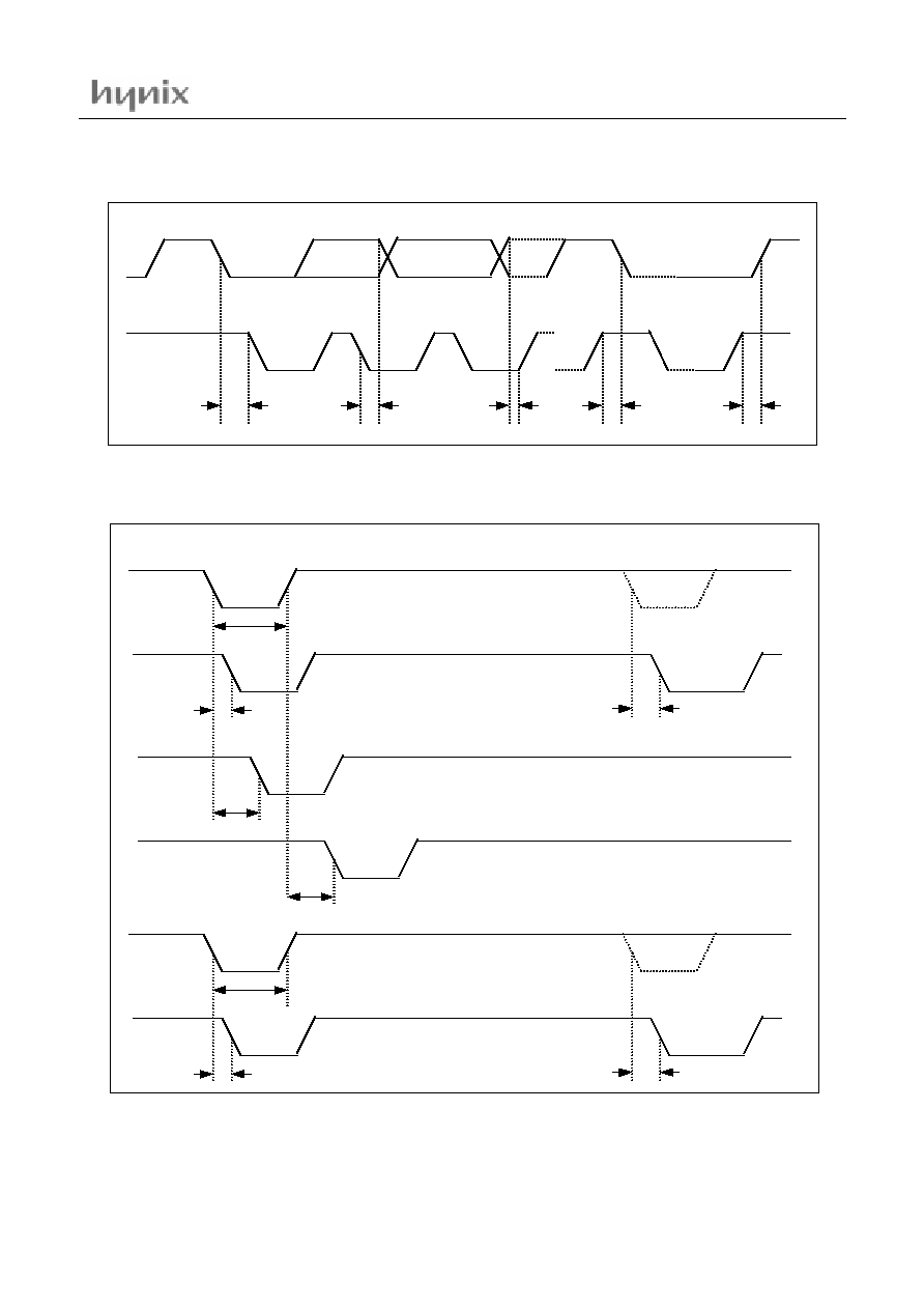
Figure 7-1 timing on the I2C-bus
Figure 7-2 SYNC timing
SDA
SCL
t
HD(SDA)
t
HD(DAT)
t
SU(DAT)
t
SU(STA)
t
SU(STO)
HSYNCin
HSYNCout
t
D(HSYNC)
t
D,MAX(HSYNC)
t
W(HSYNC)
CLAMP
(front porch)
t
D(CLAMP)
t
D(CLAMP)
CLAMP
(back porch)
VSYNCin
VSYNCout
t
D(VSYNC)
t
D,MAX(VSYNC)
t
W(VSYNC)
HMS91C7134
16
November.2001 ver1.0
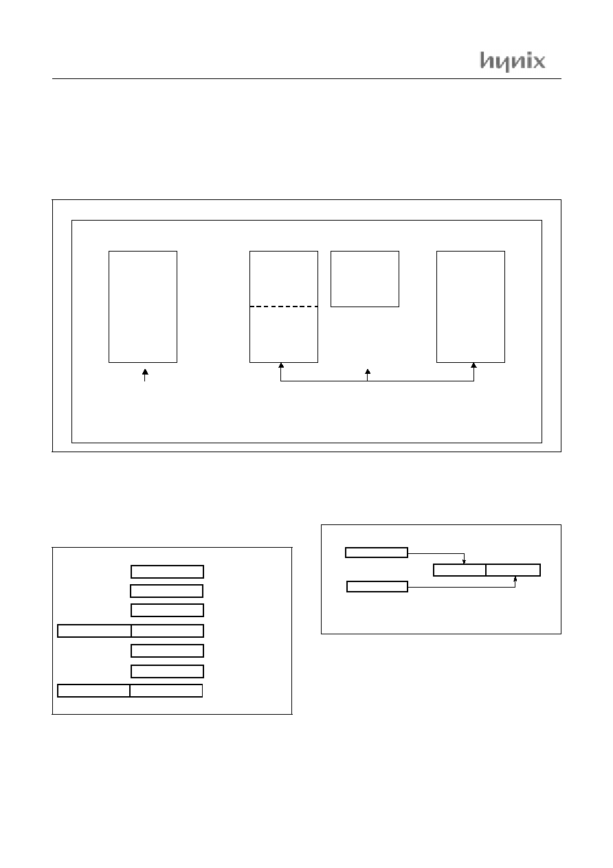
8. MEMORY ORGANIZATION
The HMS91C7132 has separate address spaces for Program
memory, Data Memory. Program memory can only be read, not
written to. It can be up to 32K bytes of Program memory.(OPT
type: HMS97C7134 32K bytes)
Data memory can be read and written to up to 256 bytes including
the stack area.(Internal RAM) and 256bytes (External RAM:
256bytes of XRAM0).
Figure 8-1 Memory map and address spaces
8.1 Registers
This device has several registers that are the Program Counter
(PC), Accumulator (A), B register(B), the Stack Pointer (SP), the
P r o g r a m S t a t u s W o r d ( P S W ) , G e n e r a l p u r p o s e r e g i s -
ter(R0~R7)and DPTR(Data pointer register).
Figure 8-2 Configuration of Registers
Accumulator: The Accumulator is the 8-bit general purpose reg-
ister, used for data operation such as transfer, temporary saving,
and conditional judgement, etc. The Accumulator can be used as
a 16-bit register with B Register as shown below.
Figure 8-3 Configuration of BA 16-bit Registers
B Register: The B Register is the 8-bit purpose register, used for
an arithmatic operation such as multiply, division with Accumu-
lator
Stack Pointer: The Stack Pointer is an 8-bit register used for oc-
currence interrupts and calling out subroutines. Stack Pointer
identifies the location in the stack to be access (save or re-
store).The stack can be located at any position within 0000
H
to
007F
H
of the internal data memory. The SP is not initialized by
hardware, requiring to write the initial value (the location with
32K ROM
Indirect
only
("mov @ri")
Direct("mov")
or Indirect
("mov @ri")
0
127
255
Direct
("mov") or
Indirect
("mov @ri" )
Indirect
("movx @ri" or
movx @dptr)
(XRAMS = 0)
data memory
program memory
SFR
XRAM
RAM
A
ACCUMULATOR
STACK POINTER
PROGRAM COUNTER
PROGRAM STATUS
WORD
SP
PCL
PCH
PSW
R0~R7
GENERAL PURPOSE
B
B REGISTER
REGISTER (BANK0~3)
DPTR(DPL)
DPTR(DPH)
DATA POINTER
REGISTER
Two 8-bit Registers can be used as a "BA" 16-bit Register
B
A
B
A
HMS91C7134
November.2001 ver1.0
17
which the use of the stack starts) by using the initialization rou-
tine. Normally, the initial value of "07
H
" is used and the stack
area is 00
H
to 7F
H
.
Program Counter: The Program Counter is a 16-bit wide which
consists of two 8-bit registers, PCH and PCL. This counter indi-
cates the address of the next instruction to be executed. In reset
state, the program counter has reset routine address (PC
H
:0FF
H
,
PC
L
:0FE
H
).
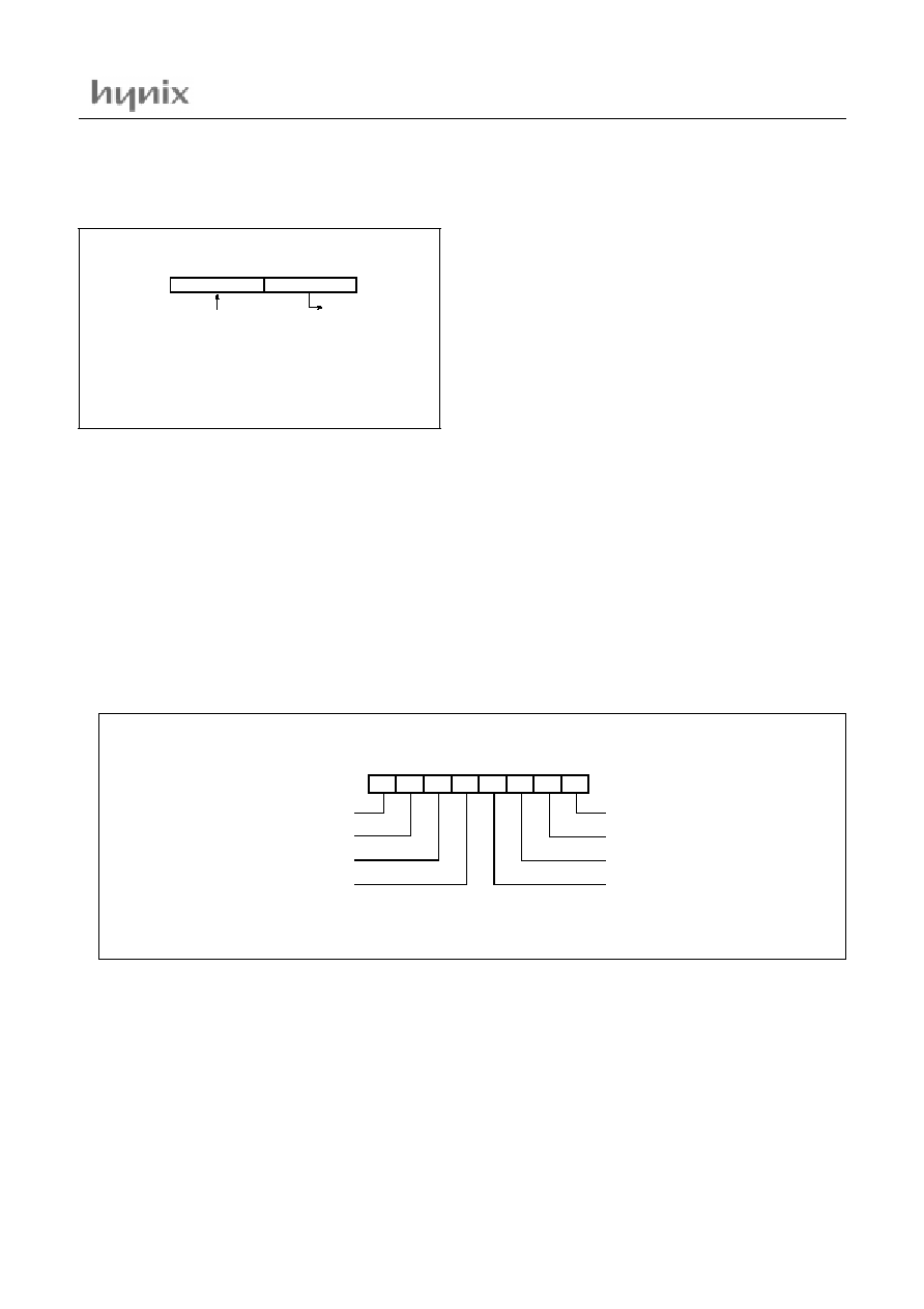
Program Status Word: The Program Status Word (PSW) con-
tains several bits that reflect the current state of the CPU and se-
lect Internal RAM(00H~1FH:Bank0~Bank3). The PSW is
described in Figure 8-4. It contains the Carry flag, the Auxiliary
carry flag, the Half Carry (for BCD operation), the General pur-
pose flag, the Register bank select flags, the Overflow flag, the
undefined flag and Parity flag.
[Carry flag CY]
This flag stores any carry or not borrow from the ALU of CPU
after an arithmetic operation and is also changed by the Shift In-
struction or Rotate Instruction.
[Auxiliary carry flag AC]
After operation, this is set when there is a carry from bit 3 of ALU
or there is no borrow from bit 4 of ALU.
[Register bank select flags RS0, RS1]
This flags select one of four bank(00~07H:bank0, 08~0fH:bank1,
10~17H:bank2, 17~1FH:bank3)in Internal RAM.
[Overflow flag OV]
This flag is set to "1" when an overflow occurs as the result of an
arithmetic operation involving signs. An overflow occurs when
the result of an addition or subtraction exceeds +127(7F
H
) or -
128(80
H
). The CLRV instruction clears the overflow flag. There
is no set instruction. When the BIT instruction is executed, bit 6
of memory is copied to this flag.
[Parity flag P]
This flag reflect on number of Accumulator's 1. If number of Ac-
uumulator's 1 is odd, P=0. otherwise P=1. Sum of adding Acu-
umulator's 1 to P is always even.
R0~R7: General purpose register.
Data Pointer Register:Data Pointer Register is 16-bit wide
which consists of two-8bit registers, DPH and DPL. This register
is used as a data pointer for the data transmission with external
data memory.
Figure 8-4 PSW(Program Status Word)Register
8.2 Program Memory
The program memory consists of ROM : 32K bytes (HMS91C7132) and 32K bytes (HMS97C7134)
8.3 Data memory
The internal data memory is divided into four physically separat-
ed part : 256 bytes of RAM, 256 bytes of XRAM0, and 128 bytes
of Special Function Registers (SFRs) areas.
RAM
Four register banks, each 8 registers wide, occupy locations 0
through 31 in the lower RAM area. Only one of these banks may
be enabled at a time. The next 16 bytes, locations 32 through 47,
SP
00
H
Stack Area (30
H
~ 7F
H
)
Bit 15
Bit 0
8 7
Hardware fixed
00
H
~7F
H
SP (Stack Pointer) could be in 00
H
~7F
H
.
CARRY FLAG
MSB
LSB
RESET VALUE: 00
H
PSW
AUXILIARY CARRY FLAG
REGISTER BANK SELECT FLAG
PARITY FLAG
NOT ASSIGNED BIT
OVERFLOW FLAG
REGISTER BANK SELECT FLAG
GENERAL PURPOSE FLAG
C Y
AC
F0
R S1 R S0 0V
P
(to select Bank0~3 with RS0)
(to select Bank0~3 with RS1)
HMS91C7134
18
November.2001 ver1.0
contain 128 directly addressable bit locations.The stack depth is
only limited by the available internal RAM space of 256 bytes.
XRAM0
The 256 bytes of XRAM0 used to support DDC interface is also
available for system usage by indirect addressing through the ad-
dress pointer DDCADR and data I/O buffer RAMBUF. The ad-
dress pointer(DDCADR) is equipped with the postincrement
capability to facilitate the transfer of data in bulk (for details refer
to DDC Interface part). However, it is also possible to address the
DRAM through MOVX command as usually used in the internal
RAM extension of 80C51 derivatives. XRAM0 0 to 255 is direct-
ly addressable as external data memory locations 0 to 255 via
MOVX-DPTR instruction or via MOVX-Ri instruction when the
EXCON's LSB is zero. Since external access function is not
available, any access to XRAM0 0 to 255 will not affect the
ports.
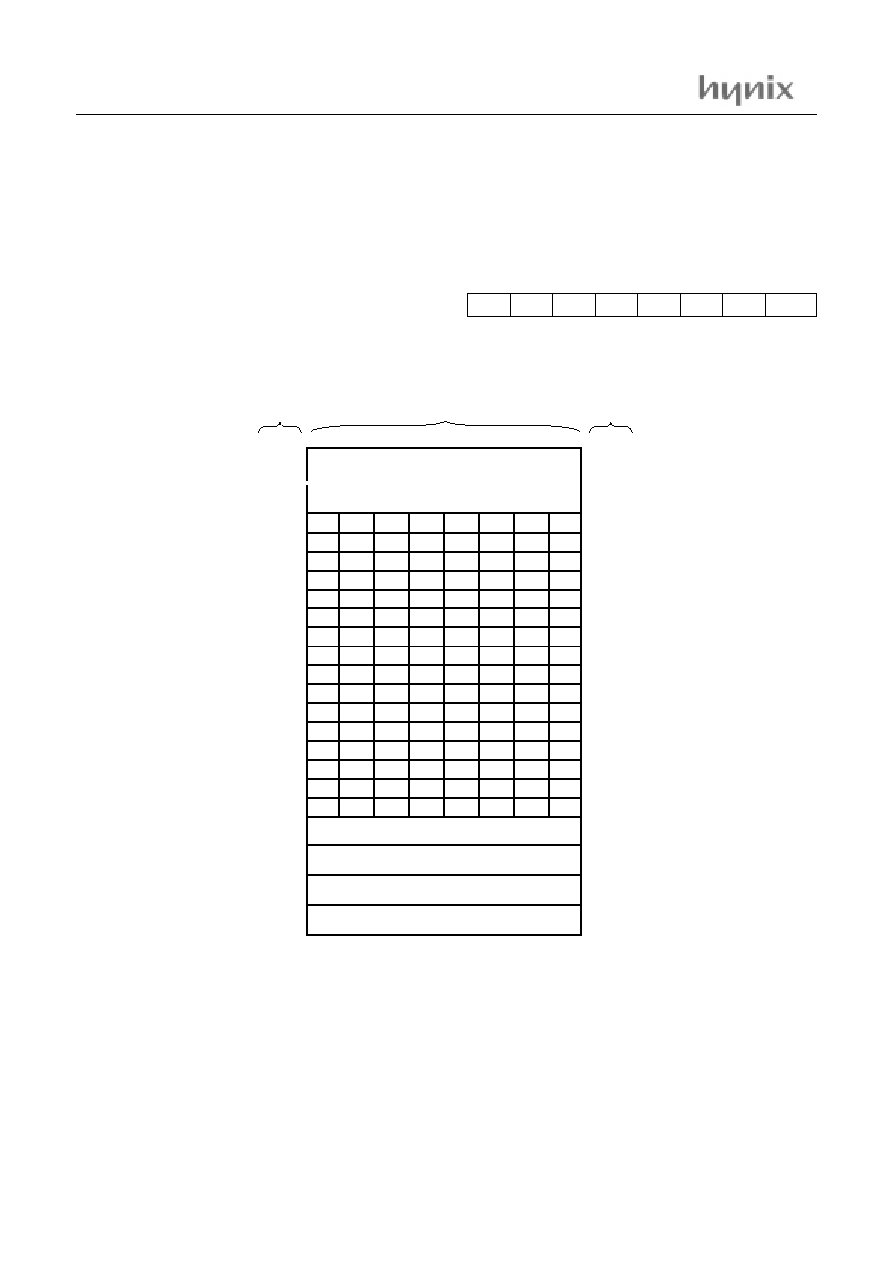
7 6 5 4 3 2 1 0
Table 8-1 Extended control Register(EXCON)
Figure 8-5 RAM ADDRESS
-
-
-
-
-
-
-
XRAMS
B A N K 3
B A N K 2
B A N K 1
B A N K 0
00 H
07 H
08 H
0F H
10 H
17 H
1F H
18 H
2F H
2E H
2D H
2C H
2B H
2A H
29 H
28 H
27 H
26 H
25 H
24 H
23 H
22 H
21 H
20 H
F F H
0
7
8
1 5
1 6
2 3
3 1
2 4
4 7
4 6
4 5
4 4
4 3
4 2
4 1
4 0
3 9
3 8
3 7
3 6
3 5
3 4
3 3
3 2
2 55
(M S B )
(LS B )
1F
1 E
1D
1 C
1 B
1A
1 9
18
17
1 6
15
1 4
1 3
12
1 1
10
0F
0 E
0D
0 C
0 B
0A
0 9
08
07
0 6
05
0 4
0 3
02
0 1
00
3F
3 E
3D
3 C
3 B
3A
3 9
38
37
3 6
35
3 4
3 3
32
3 1
30
2F
2 E
2D
2 C
2 B
2A
2 9
28
27
2 6
25
2 4
2 3
22
2 1
20
5F
5 E
5D
5 C
5 B
5A
5 9
58
57
5 6
55
5 4
5 3
52
5 1
50
4F
4 E
4D
4 C
4 B
4A
4 9
48
47
4 6
45
4 4
4 3
42
4 1
40
7F
7 E
7D
7 C
7 B
7A
7 9
78
77
7 6
75
7 4
7 3
72
7 1
70
6F
6 E
6D
6 C
6 B
6A
6 9
68
67
6 6
65
6 4
6 3
62
6 1
60
~
~
B Y T E
A D D R E S S
(H E X )
B IT
A D D R E S S
(H E X )
B Y T E
A D D R E S S
(D E C IM A L)
~
~
HMS91C7134
November.2001 ver1.0
19
SFR
The SFRs can only be addressed directly in the address range
from 128 to 255. Table 8.2 gives an overview of the Special Func-
tion Registers space. Sixteen address in the SFRs space are both-
byte and bit-addressable. The bit-addressable SFRs are those
whose address ends in 0H and 8H. The bit addresses in this area
are 80H to FFH.
Table 8-2 SFR Memory Map
Note: * The register that can be bit-addressing.
F8
-
HVGEN
CPGEN
VFH
VFL
HFH
HFL
FF
F0
*B
MDCON
MDST
VPH
HPH
VHPL
F7
E8
*EXCON
-
-
-
EF
E0
*ACC
-
-
-
-
-
-
E7
D8
*S1CON
S1STA
S1DAT
S1ADR0
S2CON
S2STA
S2DAT
S2ADR
DF
D0
*PSW
S1SDR1
RAMBUF
DDCDAT
DDCADR
DDCCON
D7
C8
*T2CON
-
RC2L
RC2H
-
-
CF
C0
-
-
C7
B8
*IP
-
BF
B0
*P3
DPWMCON
DPWM0
DPWM1
-
IPA
-
B7
A8
*IE
-
PWM4
PWM5
PWM6
PWM7
WDTKEY
AF
A0
*P2
PWMCON
PWM0
PWM1
PWM2
PWM3
WDTRST
IEA
A7
98
-
-
9F
90
*P1
P1SFS
P2SFS
P3SFS
ADAT
ACON
97
88
*TCON
TMOD
TL0
TL1
TH0
TH1
8F
80
*P0
SP
DPL
DPH
PCON
87
HMS91C7134
20
November.2001 ver1.0
8.4 List of SFRS
Register
Description
Address
R/W
Initial Value
7 6 5 4 3 2 1 0
P0
Port0 Register
80H
R/W
1 1 1 1 1 1 1 1
SP
Stack Point register
81H
R/W
0 0 0 0 0 1 1 1
DPL
Data Pointer(Low byte) Register
82H
R/W
0 0 0 0 0 0 0 0
DPH
Data Pointer(High byte) Register
83H
R/W
0 0 0 0 0 0 0 0
PCON
Power Control Register
87H
R/W
x x 0 0 0 0 0 0
TCON
Timer/Counter Control Register
88H
R/W
0 0 0 0 0 0 0 0
TMOD
Timer/Counter Mode Control Register
89H
R/W
0 0 0 0 0 0 0 0
TL0
Timer/Counter0 Low byte Register
8AH
R/W
0 0 0 0 0 0 0 0
TL1
Timer/Counter1 Low byte Register
8BH
R/W
0 0 0 0 0 0 0 0
TH0
Timer/Counter0 High byte Register
8CH
R/W
0 0 0 0 0 0 0 0
TH1
Timer/Counter1 High byte Register
8DH
R/W
0 0 0 0 0 0 0 0
P1
Port1 Register
90H
R/W
1 1 1 1 1 1 1 1
P1SFS
Port1 Special Function Selection Register
91H
R/W
0 0 0 0 0 0 0 0
P2SFS
Port2 Special Function Selection Register
92H
R/W
0 0 0 0 0 0 0 0
P3SFS
Port3 Special Function Selection Register
93H
R/W
0 0 0 0 0 0 0 0
ADAT
ADC Data Register
96H
R/W
0 0 0 0 0 0 0 0
ACON
ADC Control Register
97H
R/W
x x 0 x 0 0 0 1
P2
Port2 Register
0A0H
R/W
1 1 1 1 1 1 1 1
PWMCON
PWM Control Register
0A1H
R/W
0 0 0 0 0 0 0 0
PWM0
PWM0 Output Register
0A2H
R/W
1 1 1 1 1 1 1 1
PWM1
PWM1 Output Register
0A3H
R/W
1 1 1 1 1 1 1 1
PWM2
PWM2 Output Register
0A4H
R/W
1 1 1 1 1 1 1 1
PWM3
PWM3 Output Register
0A5H
R/W
1 1 1 1 1 1 1 1
PWM4
PWM4 Output Register
0AAH
R/W
1 1 1 1 1 1 1 1
PWM5
PWM5 Output Register
0ABH
R/W
1 1 1 1 1 1 1 1
PWM6
PWM6 Output Register
0ACH
R/W
1 1 1 1 1 1 1 1
PWM7
PWM7 Output Register
0ADH
R/W
1 1 1 1 1 1 1 1
WDTKEY
Watchdog Key Register
0AEH
R/W
0 0 0 0 0 0 0 0
WDTRST
Watchdog Timer Reset Register
0A6H
R/W
0 0 0 0 0 0 0 0
IEA
Interrupt Enable Register
0A7H
R/W
0 x x x x x 0 0
IE
Interrupt Enable Register
0A8H
R/W
0 0 0 0 0 0 0 0
P3
Port3 Register
0B0H
R/W
1 1 1 1 1 1 1 1
DPWMCON
Dynamic PWM Control Register
0B1H
R/W
0 x x x x x 0 0
DPWM0
Dynamic PWM0 Output Register
0B2H
R/W
1 1 1 1 1 1 1 1
DPWM1
Dynamic PWM1 Output Register
0B3H
R/W
1 1 1 1 1 1 1 1
IPA
Interrupt Priority Register
0B6H
R/W
0 x x x x x 0 0
IP
Interrupt Priority Register
0B8H
R/W
x 0 0 0 0 0 0 0
T2CON
Timer2 Control Register
0C8H
R/W
0 x x x x 0 x x
RC2L
Reload Low Register
0CAH
R/W
0 0 0 0 0 0 0 0
RC2H
Reload High Register
0CBH
R/W
0 0 0 0 0 0 0 0
PSW
Program Status Word Register
0D0H
R/W
0 0 0 0 0 0 0 0
RAMBUF
RAM Buffer I/O Interface Register
0D4H
R/W
x x x x x x x x
HMS91C7134
November.2001 ver1.0
21
DDCDAT
Data Shift Register for DDC1
0D5H
R/W
0 0 0 0 0 0 0 0
DDCADR
DDC Address Pointer Register
0D6H
R/W
0 0 0 0 0 0 0 0
DDCCON
DDC Mode Status and DDC1 Control Register
0D7H
R/W
x 0 0 x 0 0 0 0
S1CON
Serial Control Register for DDC2
0D8H
R/W
0 0 0 0 0 0 0 0
S1STA
Serial Status Register for DDC2
0D9H
R
0 x 0 0 x x x x
S1DAT
Data Shift Register for DDC2
0DAH
R/W
0 0 0 0 0 0 0 0
S1ADR0
Serial Address0 Register for DDC2
0DBH
R/W
0 0 0 0 0 0 0 x
S1ADR1
Serial Address1 Register for DDC2
0D3H
R/W
0 0 0 0 0 0 0 x
S2CON
Serial Control Register
0DCH
R/W
0 0 0 0 0 0 0 0
S2STA
Serial Status Register
0DDH
R
0 x 0 0 x x x x
S2ADR
Serial Address Register for I2C
0DFH
R/W
0 0 0 0 0 0 0 x
S2DAT
Data Shift Register for I2C
0DEH
R/W
0 0 0 0 0 0 0 0
ACC
Accumulator 0E0H
R/W
0 0 0 0 0 0 0 0
EXCON
Extended Control Register
0E8H
R/W
x x x x x x x 0
B
B Register
0F0H
R/W
0 0 0 0 0 0 0 0
MDCON
Mode Indication Register
0F1H
R/W
0 0 0 x x 0 0 0
MDST
Mode Status Register
0F2H
R
x 0 0 0 0 0 0 0
VPH
Vertical scan period High byte Register
0F3H
R/W
0 0 0 0 0 0 0 0
HPH
Horizontal scan period High byte Register
0F4H
R/W
0 0 0 0 0 0 0 0
VHPL
V/H scan period High byte Register
0F5H
R/W
0 0 0 0 0 0 0 0
HVGEN
H/V pulse Control Register
0F9H
R/W
x 0 0 0 x 0 0 0
CPGEN
Clamping pulse and Pattern Control register
0FAH
R/W
0 0 0 0 0 x 0 0
VFH
Vertical free-running output pulse period High byte
register
0FBH
R/W
0 0 1 0 0 0 0 0
VFL
Vertical free-running output pulse period Low byte
register
0FCH
R/W
0 0 0 0 1 0 1 0
HFH
Horizontal free-running output pulse period High
byte register
0FDH
R/W
0 1 1 0 0 0 0 0
HFL
Horizontal free-running output pulse period Low
byte register
0FEH
R/W
0 0 x 1 1 1 1 1
Register
Description
Address
R/W
Initial Value
7 6 5 4 3 2 1 0
HMS91C7134
22
November.2001 ver1.0
8.5 Addressing Mode
The addressing modes in HMS9xC7134 instruction set are as follows
· Direct addressing
· Indirect addressing
· Register addressing
· Register-specific addressing
· Immediate constants addressing
· Indexed addressing
Note that refer to "Chapter 22. Instruction Set" those addressing modes and related instructions.
(1) Direct addressing
In a direct addressing the operand is specified by an 8-bit address
f i el d in t h e i n s tr u c ti o n . On l y in t e rn a l D at a R AM a n d
SFRs(80~FFH RAM) can be directly addressed.
Example:
mov A, 3EH ; A
RAM[3E]
(2) Indirect addressing
In indirect addressing the instruction specifies a register which
contains the address of the operand. Both internal and external
RAM can be indirectly addressed. The address register for 8-bit
addresses can be R0 or R1 of the selected register bank, or the
Stack Pointer. The address register for 16-bit addresses can only
be the 16-bit "data pointer" register, DPTR.
Example:
mov @R1, 40H
;[R1]
H]
(3) Register addressing
The register banks, containing registers R0 through R7, can be
accessed by certain instructions which carry a 3-bit register spec-
ification within the opcode of the instruction. Instructions that ac-
cess the registers this way are code efficient, since this mode
eliminates an address byte. When the instruction is executed, one
of four banks is selected at execution time by the two bank select
bits in the PSW.
Example; mov PSW, #0001000B ; select Bank0
mov A, #30H
mov R1, A
(4) Register-specific addressing
Some instructions are specific to a certain register. For example,
some instructions always operate on the Accumulator, or Data
Pointer, etc., so no address byte is needed to point it. The opcode
itself does that.
A
04
PROG. MEMORY
3E
H
55
40
H
~
~
~
~
55
R1
PROG. MEMORY
HMS91C7134
November.2001 ver1.0
23
(5) Immediate constants addressing
The value of a constant can follow the opcode in Program mem-
ory.
Example; mov A, #100H.
(6)Indexed addressing
Only Program memory can be accessed with indexed addressing,
and it can only be read. This addressing mode is intended for
reading look-up tables in Program memory. A 16-bit base register
(either DPTR or PC) points to the base of the table, and the Ac-
cumulator is set up with the table entry number. The address of
the table entry in Program memory is formed by adding the Ac-
cumulator data to the base pointer.
Example; movc A, @A+DPTR
1EAD
H
~
~
~
~
ACC
DPTR
3A
1E73
PROG. MEMORY

HMS91C7134
24
November.2001 ver1.0
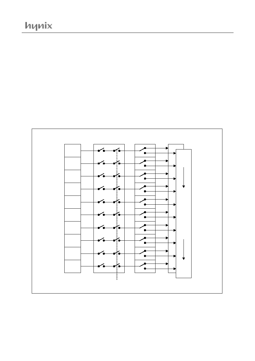
9. INTERRUPTS
There are interrupt requests from 9 sources as follows.
· INT0 external interrupt
· INT1 external interrupt
·Timer0 interrupt
· Timer1 interrupt
· Timer2 interrupt
· DDC interrupt
· MD interrupt
· VSYNC interrupt
· I2C interrupt
9.1 Interrupt sources
INT0 external interrupt:
·The INT0 can be either level-active or transition-active depend-
ing on bit IT0 in register TCON. The flag that actually generates
this interrupt is bit IE0 in TCON.
·
When an external interrupt is generated, the corresponding re-
quest flag is cleared by the hardware when the service routine is
vectored to only if the interrupt was transition-activated.
· I
f the interrupt was level-activated then the interrupt request flag
remains set until the requested interrupt is actually generated.
Then it has to deactivate the request before the interrupt service
routine is completed, or else another interrupt will be generated.
INT1 external interrupt:
·T
he INT1 can be either level-active or transition-active depend-
ing on bit IT1 in register TCON. The flag that actually generates
this interrupt is bit IE1 in TCON.
·
When an external interrupt is generated, the corresponding re-
quest flag is cleared by the hardware when the service routine is
vectored to only if the interrupt was transition-activated.
· If the interrupt was level-activated then the interrupt request flag
remains set until the requested interrupt is actually generated.
Then it has to deactivate the request before the interrupt service
routine is completed, or else another interrupt will be generated.
MD interrupt:
·A MD interrupt is generated by the hardware mode detector in
case of mode change, horizontal or vertical.
· This flag has to be cleared by the software.
VSYNC interrupt:
·The changing of the VSYNC level can generate an interrupt.
This depends on the setting that is programmed in the MDCON-
SFR. Via this register it is possible to enable the edge of the
VSYNC-signal that should generate the interrupt. Both edges can
be controlled separately.
· The interrupt flag has to be cleared by the software.
DDC interrupt:
·The DDC interrupt is generated either by bit INTR in the S1STA
register for DDC2B/DDC2AB/DDC2B+ protocol or by bit
DDC_int in the DDCCON register for DDC1 protocol or by bit
SWHINT bit in the DDCCON register when DDC protocol is
changed from DDC1 to DDC2.
· Flags except the INTR have to be cleared by the software. INTR
flag is cleared by hardware.
I2C interrupt:
·The interrupt of the second I2C is generated by bit INTR in the
register S2STA.
· This flag is cleared by hardware.
HMS91C7134
November.2001 ver1.0
25
Timer0 and Timer1 interrupt:
·Timer0 and Timer1 interrupts are generated by TF0 and TF1
which are set by an overflow of their respective Timer/Counter
registers(except for Timer0 in mode3).
·These flags are cleared by the internal hardware.
Timer2 interrupt:
·Timer2 interrupt is generated by TF2 which is set by an overflow
of Timer2.
· This flag has to be cleared by the software.
All of the bits that generate interrupts can be set or cleared by software, with the same result as though it had been set or
cleared by hardware. That is, interrupts can be generated or pending interrupts can be cancelled in software.
Figure 9-1 Interrupt system
INT0
MD
Timer0
I2C
INT1
DDC
Timer1
VSYNC
Not
used
Timer2
High
Low
In
te
rru
p
t
P
o
ll
in
g
S
e
q
u
e
n
c
e
Interrupt
Sources
IE / IEA
IP / IPA
Priority
Global
Enable
HMS91C7134
26
November.2001 ver1.0
9.2 Interrupt Enable structure
Each interrupt source can be individually enabled or disabled by
setting or clearing a bit in the interrupt enable special function
register IE and IEA. All interrupt source can also be globally dis-
abled by clearing bit EA in IE.
Table 9-1 Interrupt Enable Register(IE: 0A8H) RESET VALUE:00000000B
Table 9-2 Description of the IE bits
Table 9-3 Interrupt Enable Register(IEA: 0A7H) RESET VALUE:0xxxxx00B
Table 9-4 Description of Enable Register(IEA: 0A7H)
7
6
5
4
3
2
2
0
EA
EVSYNC
ET2
ES
ET1
EX1
ET0
EX0
BIT
SYMBOL
FUNCTION
7
EA
Disable all interrupts.
0 : no interrupt will be acknowledged
1 : each interrupt source is individually enabled or disabled by setting or clear
ing its enable bit
6
EVSYNC
Enable Vsync interrupt
5
ET2
Enable timer2 interrupt
4
ES
Not used
3
ET1
Enable timer1 interrupt
2
EX1
Enable external interrupt (INT1)
1
ET0
Enable timer0 interrupt
0
EX0
Enable external interrupt (INT0)
7
6
5
4
3
2
2
0
EDDC
-
-
-
-
-
EI2C
EMD
BIT
SYMBOL
FUNCTION
7
EDDC
Enable DDC interrupt
6
EX6
Not used
5
EX5
Not used
4
EX4
Not used
3
EX3
Not used
2
EX2
Not used
1
EI2C
Enable I2C interrupt
0
EMD
Enable MD interrupt
HMS91C7134
November.2001 ver1.0
27
9.3 Interrupt Priority structure
Each interrupt source can be assigned one of two priority levels.
Interrupt priority levels are defined by the interrupt priority spe-
cial function register IP and IPA.
"0" - low priority
"1" - high priority
A low priority interrupt may be interrupted by a high priority in-
terrupt level interrupt. A high priority interrupt routine cannot be
interrupted by any other interrupt source. If two interrupts of dif-
ferent priority occur simultaneously, the high priority level re-
quest is serviced. If requests of the same priority are received
simultaneously, an internal polling sequence determines which
request is serviced. Thus, within each priority level, there is a sec-
ond priority structure determined by the polling sequence. This
second priority structure is shown in Table 9.5.
Table 9-5 Priority levels
Note
· The "Priority within level" structure is only used to resolve
simultaneous requests of the same priority level.
· The MD interrupt needs a higher priority then ALL the oth-
er interrupts. This is to avoid that a mode change will not be
serviced in time and that the setting of the S-curve is not up-
dated in time. When the S-curve settings are not updated in
time (after a mode change) the monitor may be damaged.
Table 9-6 Interrupt Priority Register(IP: 0B8H) RESET VALUE: x0000000B
Table 9-7 Description of the IP bits
SOURCE
PRIORITY WITHIN LEVEL
INT0
MD
Timer0
I2C
INT1
DDC
Timer1
VSYNC
Timer2
1(highest)
9(lowest)
7
6
5
4
3
2
2
0
-
PVSYNC
PT2
PS
PT1
PX1
PT0
PX0
BIT
SYMBOL
FUNCTION
7
-
Reserved
6
PVSYNC
Vsync interrupt priority level
5
PT2
Timer2 interrupt priority level
4
PS
Not used
3
PT1
Timer1 interrupt priority level
2
PX1
External interrupt (INT1) priority level
1
PT0
Timer0 interrupt priority level
0
PX0
External interrupt (INT0) priority level
HMS91C7134
28
November.2001 ver1.0
Table 9-8 Interrupt Priority Register(IPA: 0B6H) RESET VALUE: 0xxxxx00B
Table 9-9 Description of the IPA bits
7
6
5
4
3
2
2
0
PDDC
-
-
-
-
-
PI2C
PMD
BIT
SYMBOL
FUNCTION
7
PDDC
DDC interrupt priority level
6
PX6
Not used
5
PX5
Not used
4
PX4
Not used
3
PX3
Not used
2
PX2
Not used
1
PI2C
I2C interrupt priority level
0
PMD
MD interrupt priority level
HMS91C7134
November.2001 ver1.0
29
9.4 How Interrupt are handled
The interrupt flags are sampled at S5P2 of every machine cycle.
The samples are polled during following machine cycle. If one of
the flags was in a set condition at S5P2 of the preceding cycle, the
polling cycle will find it and the interrupt system will generate an
LCALL to the appropriate service routine, provided this H/W
generated LCALL is not blocked by any of the following condi-
tions :
· An interrupt of equal priority or higher priority level is al-
ready in progress.
· The current machine cycle is not the final cycle in the ex-
ecution of the instruction in progress.
· The instruction in progress is RETI or any access to the
interrupt priority or interrupt enable registers.
The polling cycle is repeated with each machine cycle, and the
values polled are the values that were present at S5P2 of the pre-
vious machine cycle. Note that if an interrupt flag is active but be-
ing responded to for one of the above mentioned conditions, if the
flag is still inactive when the blocking condition is removed, the
denied interrupt will not be serviced. In other words, the fact that
the interrupt flag was once active but not serviced is not remem-
bered. Every polling cycle is new.
The processor acknowledges an interrupt request by executing a
hardware generated LCALL to the appropriate service routine.
The hardware generated LCALL pushes the contents of the Pro-
gram Counter on to the stack (but it does not save the PSW) and
reloads the PC with an address that depends on the source of the
interrupt being vectored to as shown in Table 9-10.
Execution proceeds from that location until the RETI instruction
is encountered. The RETI instruction informs the processor that
the interrupt routine is no longer in progress, then pops the top
two bytes from the stack and reloads the Program Counter. Exe-
cution of the interrupted program continues from where it left off.
Note that a simple RET instruction would also return execution
to the interrupted program, but it would have left the interrupt
control system thinking an interrupt was still in progress, making
future interrupts impossible.
Table 9-10 Vector addresses
SOURCE
VECTOR ADDRESS
INT0
0003H
MD
004BH
Timer0
000BH
I2C
0043H
INT1
0013H
DDC
003BH
Timer1
001BH
VSYNC
0033H
Timer2
002BH
HMS91C7134
30
November.2001 ver1.0
10. POWER-SAVING MODE
Two software selectable modes of reduced power consumption are implemented.
· Idle mode
· Power-down mode
The following functions are switched off when the microcontroller enters the Idle mode.
· CPU (halted)
· I2C interface (halted)
· PWM0 to PWM7 and DPWM0 to DPWM2 (reset, output = High)
· 8-bit ADC (aborted if conversion in progress)
The following functions remain active during Idle mode.
These functions may generate an interrupt or reset and thus terminate the Idle mode.
· Timer0, Timer1 and Timer2
· Watchdog timer
· DDC interface
· External interrupt
· Mode detection
In Power-down mode, the system clock is halted. Both the oscillator will be stopped after setting the bit PD in PCON.
10.1 Power control register
The modes Idle and Power-down are activated by software via the PCON register.
Table 10-1 Power control Register(PCON:87H) RESET VALUE:xx000000B
Table 10-2 Description of the PCON bits
7
6
5
4
3
2
2
0
-
-
LVREN
LVRLS
GF1
GF0
PD
IDL
BIT
SYMBOL
FUNCTION
7 to 6
-
Not used
5
LVREN
Enable low voltage reset
4
LVRLS
Select low VDD level ; 3.7V or 3.5V
3
GF1
General purpose flag bit
2
GF0
General purpose flag bit
1
PD
Activate Power-down mode
0
IDL
Activate Idle mode

HMS91C7134
November.2001 ver1.0
31
Table 10-3 External Pin Status During Idle and Power-down modes
10.2 Idle mode
The instruction that sets PCON.0 is the last instruction executed
in the normal operating mode before idle mode is activated. Once
in the idle mode, the CPU status is preserved in its entirety : Stack
pointer, Program counter, Program status word, Accumulator,
RAM and All other registers maintain their data during idle
mode.
There are three ways to terminate the idle mode.
· Activation of any enabled interrupt X0, T0, X1, T1 etc. will
cause PCON.0 to be cleared by hardware terminating Idle
mode. The interrupt is serviced, and following return from
interrupt instruction RETI, the next instruction to be execut-
ed will be the one which follows the instruction that wrote a
logic 1 to PCON.0.
· External hardware reset : the hardware reset is required
to be active for two machine cycle to complete the reset op-
eration.
· Internal watchdog reset : the microcontroller restarts after
3 machine cycles in all cases.
10.3 Power-down mode
The instruction that sets PCON.1 is the last executed prior to go-
ing into the Power-down mode. Once in Power-down mode, the
oscillator is stopped. The contents of the on-chip RAM and the
Special Function Register are preserved.
The power-down mode can be terminated by an external RESET
in the same way as in the 80C51 (but SFRs are cleared due to RE-
SET).
MODE
MEMORY
PORT0-3
SYNC
PWM
I2C
DDC
-
-
Idle
Intenal
Data
on High
High-Z
on
-
-
Power-down
Intenal
Data
High
High
High-Z
High-Z
-
-
HMS91C7134
32
November.2001 ver1.0
11. I/O PORTS
The HMS9xC7134 has four 8-bit ports (Port0, Port1, Port2 and
Port3). Port0 - Port3 are the same as in the 80C51, with the ex-
ception of the additional functions of Port1, Port2 and Port3. All
ports are bidirectional and Pins of which the alternative function
is not used may be used as normal bidirectional I/Os except
Port3.2, Port3.3 and Port3.5(These Pins can be only used as the
output).
The use of Port1- Port3 pins as alternative functions are carried
out automatically by the HMS9xC7134 provided the associated
SFR bit is set HIGH.Port0 is the type of open-drain I/O. Port0.6
and Port0.7 have the capability to drive LED.
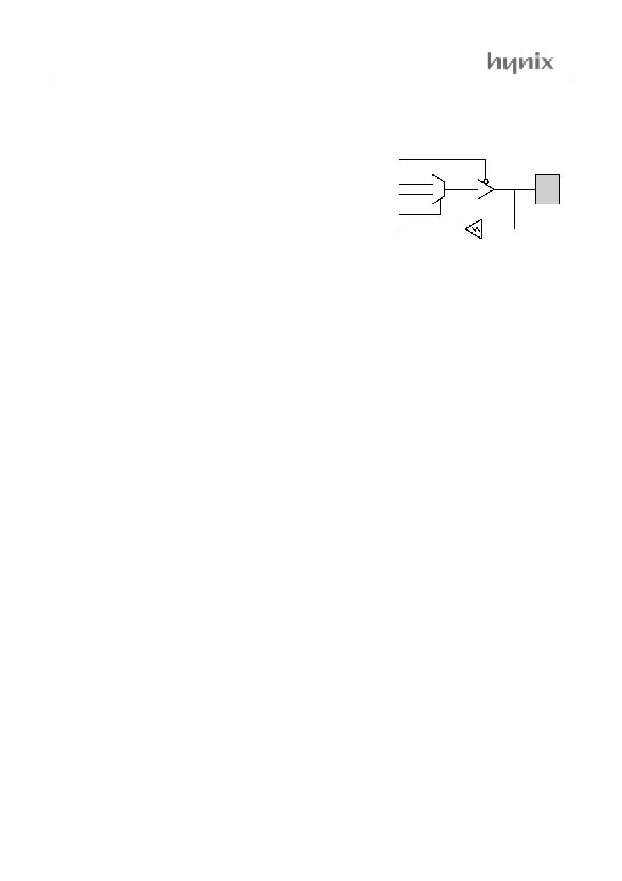
Fig. 11.1 shows the port structure.
Figure 11-1 Standard output with the open-drain port
The alternative function for Port1, Port2 and Port3 can be described as follows.
· Port 0 : No alternative function.
· Port 1 : P1.0 is combined with the SCL1 interface line(open-drain)
P1.1 is combined with the SDA1 interface line (open-drain)
P1.2 is combined with the ACH0 interface line (high-z)
P1.3 is combined with the ACH1 interface line (high-z)
P1.4 is combined with the ACH2 interface line (high-z)
P1.5 is combined with the ACH3 interface line (high-z)
P1.6 is combined with the SCL2 interface line (open-drain)
P1.7 is combined with the SDA2 interface line (open-drain)
· Port 2 : P2.0 is combined with the dynamic PWM0 interface line(open-drain or push-pull)
P2.1 is combined with the dynamic PWM1 interface line (open-drain or push-pull)
P2.2 is combined with the static PWM0 interface line (open-drain or push-pull)
P2.3 is combined with the static PWM1 interface line (open-drain or push-pull)
P2.4 is combined with the static PWM2 interface line (open-drain or push-pull)
P2.5 is combined with the static PWM3 interface line (open-drain or push-pull)
P2.6 is combined with the static PWM4 interface line (open-drain or push-pull)
P2.7 is combined with the static PWM5 interface line (open-drain or push-pull)
· Port 3 : P3.0 has not alternative function.
P3.1 has not alternative function.
P3.2 is combined with the HSYNCout interface line (push-pull)
P3.3 is combined with the VSYNCout interface line (push-pull)
P3.4 is combined with the PWM6 interface line (open-drain or push-pull)
P3.5 is combined with the CLAMP or PWM7 interface line (push-pull)
P3.6 is combined with the PATOUT interface line (push-pull)
P3.7 is combined with the SOG interface line (pull-up)
I/O PIN
Port Data
Input Data
Special Data / Gnd
Special Function Select
0
1
Enable / Data
HMS91C7134
November.2001 ver1.0
33
11.1 Pin function selection
Special function selection Registers(PxSFS)
Several SFR(P1SFS/P2SFS/P3SFS)s are used to select the port-function or the alternative function of the external pin.
· P1SFS(Port1 special function selection register)
Table 11-1 P1SFS bits(91H)
Table 11-2 Description of the P1SFS bits
7
6
5
4
3
2
2
0
P1SFS7
P1SFS6
P1SFS5
P1SFS4
P1SFS3
P1SFS2
P1SFS1
P1SFS0
BIT
SYMBOL
FUNCTION
RESET
7
P1SFS7
The selection of the pin function.
0 : pin 9 has P1.7 function.
1 : pin 9 has SDA2 function.
0
6
P1SFS6
The selection of the pin function.
0 : pin 10 has P1.6 function.
1 : pin 10 has SCL2 out function.
0
5
P1SFS5
The selection of the pin function.
0 : pin 20 has P1.5 function.
1 : pin 20 has ACH3 out function.
0
4
P1SFS4
The selection of the pin function.
0 : pin 21 has P1.4 function.
1 : pin 21 has ACH2 out function.
0
3
P1SFS3
The selection of the pin function.
0 : pin 22 has P1.3 function.
1 : pin 22 has ACH1 out function.
0
2
P1SFS2
The selection of the pin function.
0 : pin 23 has P1.2 function.
1 : pin 23 has ACH0 out function.
0
1
P1SFS1
The selection of the pin function.
0 : pin 24 has P1.1 function.
1 : pin 24 has SDA1 out function.
0
0
P1SFS0
The selection of the pin function.
0 : pin 25 has P1.0 function.
1 : pin 25 has SCL1 out function.
0
HMS91C7134
34
November.2001 ver1.0
· P2SFS(Port2 special function selection register)
Table 11-4 Description of the P2SFS bits
7
6
5
4
3
2
2
0
P2SFS7
P2SFS6
P2SFS5
P2SFS4
P2SFS3
P2SFS2
P2SFS1
P2SFS0
Table 11-3 P2SFS bits(92H)
BIT
SYMBOL
FUNCTION
RESET
7
P2SFS7
The selection of the pin function.
0 : pin 34 has P2.7 function.
1 : pin 34 has PWM5 function.
0
6
P2SFS6
The selection of the pin function.
0 : pin 35 has P2.6 function.
1 : pin 35 has PWM4 out function.
0
5
P2SFS5
The selection of the pin function.
0 : pin 36 has P2.5 function.
1 : pin 36 has PWM3 out function.
0
4
P2SFS4
The selection of the pin function.
0 : pin 37 has P2.4 function.
1 : pin 37 has PWM2 out function.
0
3
P2SFS3
The selection of the pin function.
0 : pin 38 has P2.3 function.
1 : pin 38 has PWM1 out function.
0
2
P2SFS2
The selection of the pin function.
0 : pin 1 has P2.2 function.
1 : pin 1 has PWM0 out function.
0
1
P2SFS1
The selection of the pin function.
0 : pin 2 has P2.1 function.
1 : pin 2 has DPWM1 out function.
0
0
P2SFS0
The selection of the pin function.
0 : pin 3 has P2.0 function.
1 : pin 3 has DPWM0 out function.
0
HMS91C7134
November.2001 ver1.0
35
· P3SFS(Port3 special function selection register)
Table 11-5 P3SFS bits(93H)
Table 11-6 Description of the P3SFS bits
7
6
5
4
3
2
2
0
P3SFS7
P3SFS6
P3SFS5
P3SFS4
P3SFS3
P3SFS2
P3SFS1
P3SFS0
BIT
SYMBOL
FUNCTION
RESET
7
P3SFS7
The selection of the pin function.
0 : pin 28 has P3.7 function.
1 : pin 28 has SOG input function.
0
6
P3SFS6
The selection of the pin function.
0 : pin 29 has P3.6 function.
1 : pin 29 has PATOUT out function.
0
5
P3SFS5
The selection of the pin function.
0 : pin 30 has P3.5 function.
1 : pin 30 has CLAMP or PWM7 out function.
0
4
P3SFS4
The selection of the pin function.
0 : pin 31 has P3.4 function.
1 : pin 31 has PWM6 out function.
0
3
P3SFS3
The selection of the pin function.
0 : pin 32 has P3.3 function.
1 : pin 32 has VSYNCout function.
0
2
P3SFS2
The selection of the pin function.
0 : pin 33 has P3.2 function.
1 : pin 33 has VSYNCout function.
0
1
P3SFS1
The selection of the pin function.
reserved
0
0
P3SFS0
The selection of the pin function.
reserved
0
HMS91C7134
36
November.2001 ver1.0
12. OSCIALLTOR
The oscillator circuit of the HMS9xC7134 is a single stage invert-
ing amplifier in a Pierce oscillator configuration. The circuitry
between XTAL1 and XTAL2 is basically an inverter biased to the
transfer point. Either a crystal or ceramic resonator can be used as
the feedback element to complete the oscillator circuit. Both are
operated in parallel resonance.
XTAL1 is the high gain amplifier input, and XTAL2 is the out-
put. To drive the HMS9xC7134 externally, XTAL1 is driven
from an external source and XTAL2 left open-circuit.
Figure 12-1 Oscillator configuration
Main clock
Minimum instruction cycle time
(ex:NOP ; f
ex
12clock is needed)
12MHz
1uS
XTAL1
XTAL2
XTAL1
XTAL2
External clock
10 ~ 16MHz
reset
Vdd
reset
Vdd
4.2V
ideal
standard; R=10K
C=10uF (Recommanded)
reset IC
R
C
HMS91C7134
November.2001 ver1.0
37
13. RESET
There are three ways to invoke a reset and initialize the
HMS9xC7134.
Via the external RESET pin
Via the Watchdog Timer overflow
Via low VDD voltage reset
Each reset source will cause an internal reset signal active. The
CPU responds by executing an internal reset and puts the internal
registers in a defined state.
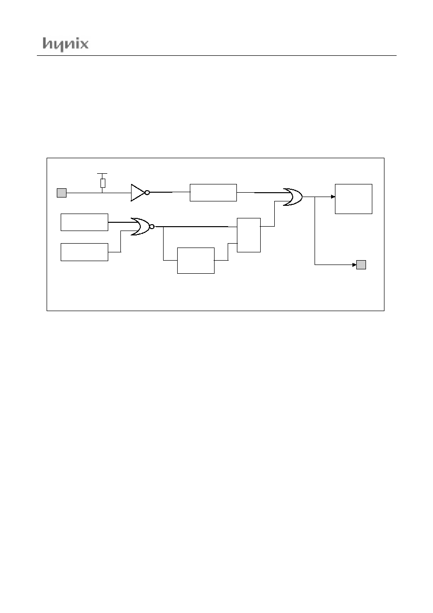
Figure 13-1 The reset mechanism
13.1 External reset
The reset pin RESET is connected to a Schmitt trigger for noise
reduction. A reset is accomplished by holding the RESET pin
LOW for at least 2 machine cycles (24 system clock), while the
oscillator is running.
An automatic reset can be obtained by switching on VDD, if the
RESET pin is connected to GND via a capacitor and to the VDD
via resistor. The capacitor should be at least 10uF.
The increase of the RESET pin voltage depends on the capacitor.
The voltage must remain below the higher threshold for at mini-
mum the oscillator start-up time plus 2 machine cycles.
13.2 Watchdog timer overflow
The length of the output pulse from the WDT is over 2048 machine cycles. In chapter 14, the watchdog timer is described in more detail.
13.3 Low VDD voltage reset
When VDD is below 3.7V, the built-in low voltage detector generates an internal reset signals. The reset signal will be LOW during 2ms
@12MHz after the voltage is higher than 3.7V.
WDT
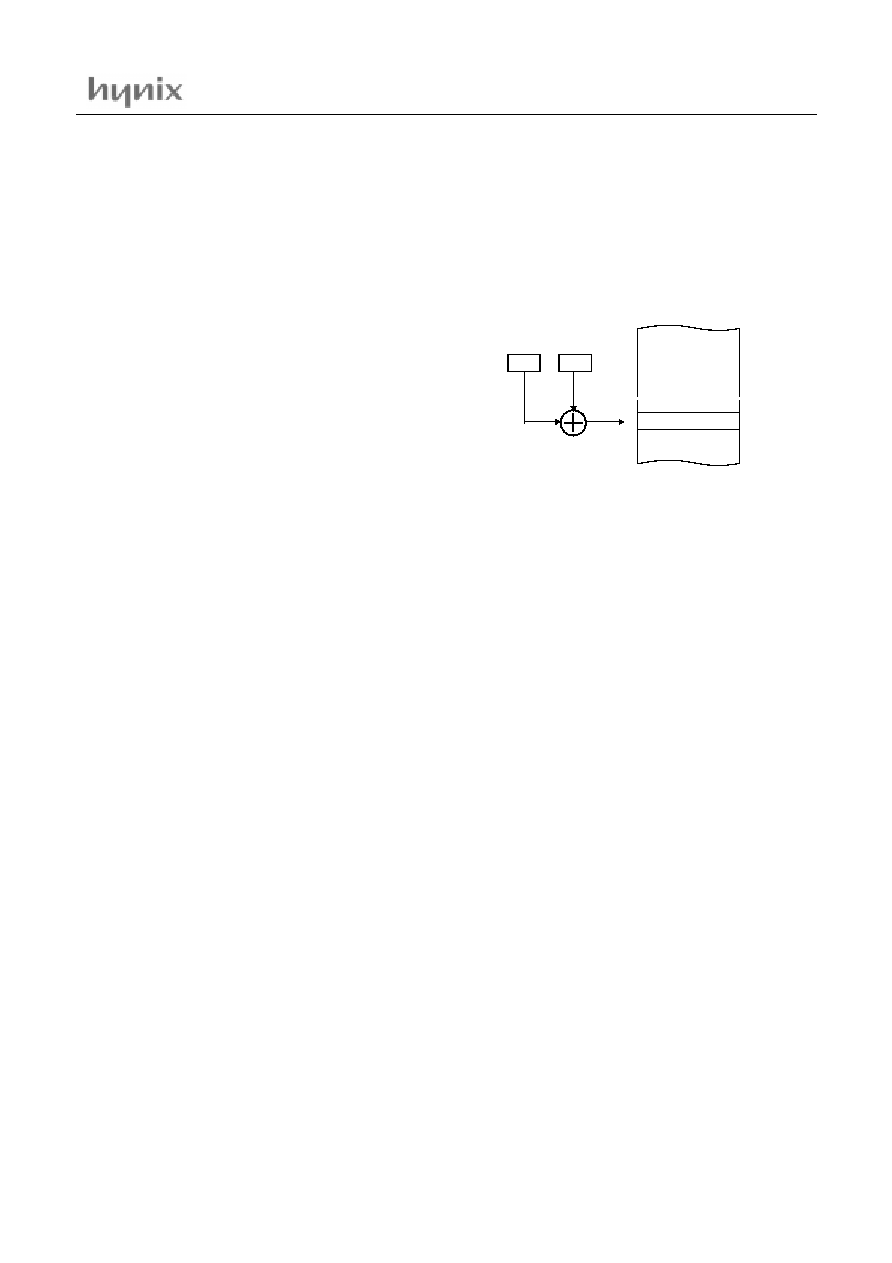
LVR
S Q
R
2.0m s
Timer
RESET
RSTOUT
CPU&
PERI.
NC
HMS91C7134
38
November.2001 ver1.0
14. WATCHDOG TIMER
The hardware watchdog timer (WDT) resets the HMS9xC7134
when it overflows. The WDT is intended as a recovery method in
situations where the CPU may be subjected to a software upset.
To prevent a system reset the timer must be reloaded in time by
the application software. If the processor suffers a hardware/soft-
ware malfunction, the software will fail to reload the timer. This
failure will result in a reset upon overflow thus preventing the
processor running out of control.
In the idle mode the watchdog timer and reset circuitry remain ac-
tive. The WDT consists of a 19-bit counter, the watchdog timer
re set(WDT RS T) S FR and watchdo g k ey reg ister(WDT-
KEY).Since the WDT is automatically enabled while the proces-
sor is running. the user only needs to be concerned with servicing
it.The 19-bit counter overflows when it reaches 524288(3FFFH).
The WDT increments once every machine cycle.
This means the user must reset the WDT at least every 524288
machine cycles (524ms @12MHz). To reset the WDT the user-
must write 01EH and then 0E1H to WDTRST. WDTRST is a
write only register. The WDT count cannot be read or written.
The watchdog timer is controlled by the watchdog key register,
WDTKEY. Only pattern 01010101(=55H), disables the watch-
dog timer. The rest of pattern combinations will keep the watch-
dog timer enabled. This security key will prevent the watchdog
timer from being terminated abnormally when the function of the
watchdog timer is needed.
In Idle mode, the oscillator continues to run. To prevent the WDT
from resetting the processor while in Idle, the user should always
set up a timer that will periodically exit Idle, service the WDT,
and re-enter Idle mode.
Table 14-1 Watchdog timer key register (WDTKEY : 0AEH) RESET VALUE:00000000B
Table 14-2 Description of the WDTKEY bits
Table 14-3 Watchdog timer clear register (WDTRST : 0A6H) RESET VALUE:00000000B
Table 14-4 Description of the WDTRST bits
Example Program; Watch Dog Timer
Reset & WDT_refresh Part
Reset:
clr EA
mov PSW, #00
mov SP, #STACK_DATA;
mov WDTKEY, #55h ; Watchdog stop
WDT_refresh:
mov WDTRST, #1Eh ; Watchdog timer reset
mov WDTRST, #0E1h ; Watchdog timer reset
mov WDTKEY, #0F0h ; Watchdog start
ret
7
6
5
4
3
2
2
0
WDTKEY7
WDTKEY6
WDTKEY5
WDTKEY4
WDTKEY3
WDTKEY2
WDTKEY1
WDTKEY0
BIT
SYMBOL
FUNCTION
7 to 0
WDTKEY7
to
WDTKEY0
Enable or disable watchdog timer.
01010101(=55H) : disable watchdog timer.
others : enable watchdog timer.
7
6
5
4
3
2
2
0
WDTRST7
WDTRST6
WDTRST5
WDTRST4
WDTRST3
WDTRST2
WDTRST1
WDTRST0
BIT
SYMBOL
FUNCTION
7 to 0
WDTKEY7
to
WDTKEY0
Enable or disable watchdog timer.
01010101(=55H) : disable watchdog timer.
others : enable watchdog timer.
HMS91C7134
November.2001 ver1.0
39
15. TIMER
HMS9xC7134 has two 16-bit timers/counters (Timer0, Timer1) to be placed in 80C51 core and one 16-bit auto-reload timer(Timer2) for
dynamic PWM.
15.1 Timer0 and Timer1
The external input pin that the Timer/Counter0 and Timer/
Counter1 in 80C51 core have is eliminated. In the timer function,
timer register is incremented every machine cycle. Thus, you can
think of it as counting machinecycles. Since a machine cycle con-
sists of 12 oscillator periods, the count rate is 1/12 of the oscilla-
tor frequency.
Timer 0, Timer 1 have four operating modes. These modes is se-
lected by bit-pairs(M1, M0) in TMOD.
Table 15-1 Timer Mode Control register(TMOD) RESET VALUE:00000000B
Table 15-2 Description of the TMOD bits
7
6
5
4
3
2
2
0
GATE
C/T
M1
M0
GATE
C/T
M1
M0
BIT
SYMBOL
FUNCTION
7,3
GATE
Gating control when set. Timer "x" is enabled only while "INTx" pin is high
and "TRx" control bit is set. When cleared Timer"x" is enabled whenever
"TRx"control bit is set.
6,2
C/T
Timer or Counter selector
0 : Timer
1 : Counter, not supported.
7 to 0
M1, M0
0, 0
0, 1
1, 0
1, 1
Operating modes
8-bit Timer °THx" with "TLx" as 5-bit prescaler
16-bit Timer "THx" and "TLx" are cascaded : there is no prescaler
8-bit auto-reload Timer "THx" holds a value which is to be reloaded into
"TLx" each time it overflows.
Timer0 : TL0 is an 8-bit Timer controlled by the standard
Timer 0 control bit.
: TH0 is an 8-bit timer only controlled by Timer 1 control bit.
Timer1 : Timer 1 stopped.
HMS91C7134
40
November.2001 ver1.0
Table 15-3 Timer Control register(TCON) RESET VALUE:00000000B
Table 15-4 Description of the TCON bits
15.2 TIMER2
Timer2 is a 16-bit auto-reload timer. The 16-bit capture mode,
baud rate generation mode and an event counter function that the
Timer/Counter2 in 80C52 core has are eliminated. Since the
clock of this timer comes from the system oscillator, Timer2 can
be used to count a time period more accurately comparing with
Timer0 and Timer1, but the longest period is limited as 65536 x
(tOSC/2).
The interval between interrupt =
65536 x (2 x tOSC) - (RC2H x 256 + RC2L) x (2 x tOSC)
The maximum interrupt period =
65536 x (2 x tOSC)
Table 15-5 Timer2 control register (T2CON : 0C8H) RESET VALUE:0xxxx0xxB
Table 15-6 Description of the TCON bits
7
6
5
4
3
2
2
0
TF1
TR1
TF0
TR0
IE1
IT1
IE0
IT0
BIT
SYMBOL
FUNCTION
7
TF1
Timer1 overflow flag. Set by hardware on Timer oveflow.
Cleared by hardware when processor vectors to interrupt routine.
6
TR1
Timer1 run control bit. Set/cleared by software to turn Timer on/off .
5
TF0
Timer0 overflow flag. Set by hardware on Timer oveflow.
Cleared by hardware when processor vectors to interrupt routine.
4
TR0
Timer0 run control bit. Set/cleared by software to turn Timer on/off .
3
IE1
Interrupt1 edge flag. Set by hardware when external interrupt edge detected.
Cleared when interrupt processed.
2
IT1
Interrupt1 type control bit. Set/cleared by software to specified falling
edge/low level triggered external interrupts.
1
IE0
I
nterrupt0 edge flag. Set by hardware when external interrupt edge detected.
Cleared when interrupt processed.
0
IT0
Interrupt0 type control bit. Set/cleared by software to specified falling
edge/low level triggered external interrupts.
7
6
5
4
3
2
2
0
TF2
-
-
-
-
TR2
-
-
BIT
SYMBOL
FUNCTION
7
TF2
Timer2 overflow flag. Set by hardware on Timer overflow.
Must be cleared by software.
6 to 3
-
Reserved
2
TR2
Timer2 run control bit. set/cleared by software to turn Timer on/off.
1 to 0
TR0
Reserved
HMS91C7134
November.2001 ver1.0
41
Table 15-7 Reload/Capture high register (RC2H : 0CBH) RESET VALUE:00000000B
Table 15-8 Reload/Capture low register (RC2L : OCAH) RESET VALUE:00000000B
Example Program; Timer
Initial & Timer1 Interrupt part
initial:
; mov IP, #00h; Interrupt Priority
mov PCON, #00;
mov TCON, #01010000B; T1, T0 enable
mov TMOD, #00010001B; 16 bit timer set
mov IE, #11001000B; Global En(7), Vsync(6), Timer1(3)
T1_Isr:
push PSW; PSW
push DPH; DPTR
push DPL;
push ACC; A
push 00h; R0
push 01h; R1
push 02h; R2
mov TH1, #0F0h; F060h to Generate 4mSec
mov TL1, #60h;
7
6
5
4
3
2
2
0
RC2H7
RC2H6
RC2H5
RC2H4
RC2H3
RC2H2
RC2H1
RC2H0
BIT
SYMBOL
FUNCTION
7 to 0
RC2H7
to
RC2H0
Reload low register bit7 to bit0
7
6
5
4
3
2
2
0
RC2L7
RC2L6
RC2L5
RC2L4
RC2L3
RC2L2
RC2L1
RC2L0
BIT
SYMBOL
FUNCTION
7 to 0
RC2L7
to
RC2L0
Reload low register bit7 to bit0
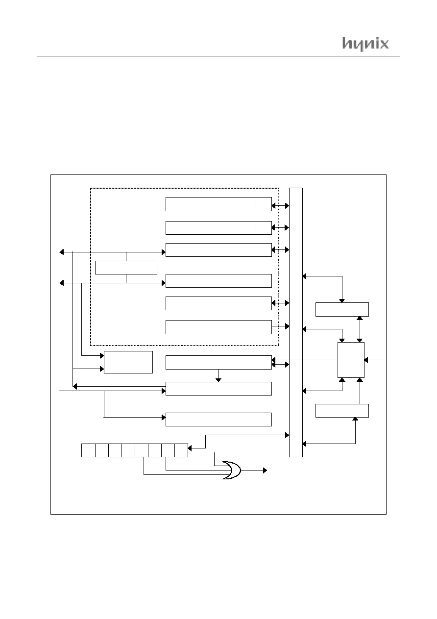
HMS91C7134
42
November.2001 ver1.0
16. DDC INTERFACE
The monitor typically includes a number of user controls to set
picture size, position, color balance, brightness and contrast.Fur-
thermore, to optimize some internal setting for different display
modes, the timing characteristics should be acquired by the con-
trol side. In these days, it is getting popular for these controls to
go to PC host. Therefore the communication between monitor
a nd host bec omes is sue.DDC1, DDC 2B , DDC 2B +, and
DDC2AB(ACCESS.bus) emerge as a standard for monitor inter-
face. A transmitter clocked by incoming VSYNC is dedicated for
DDC1 operation. An I2C interface hardware logic forms the ker-
nel of DDC2B, DDC2B+, and DDC2AB. An address pointer,
with post increment capability is employed to serve DDC1,
DDC2B,DDC2B+ and DDC2AB modes.
The conceptual block diagram is illustrated in Fig. 16.1
Figure 16-1 DDC Interface block diagram
DDC2B/DDC2AB
DDC2B+ Interface
S1ADR1
S1DAT
S1CON
S1STA
SDA1
SCL1
DDCCON
VSYNC
IN
INTR (From S1STA)
INT
DDCADR
DDCDAT
X
EX_
DAT
SW
ENB
X
DDC1
INT
DDC1
EN
SWH
INT
M0
Initialization synchronization
DDC1 transmitter
DDC1 Hold Register
Bus Clock Generator
Shift Register
Monitor Address
Arbitration Logic
DDC1/DDC2
Detection
RAMBUF
RAM
Buffer
Address Pointer
Int
e
r
n
al
B
u
s
S1ADR0
7
1
0
Monitor Address
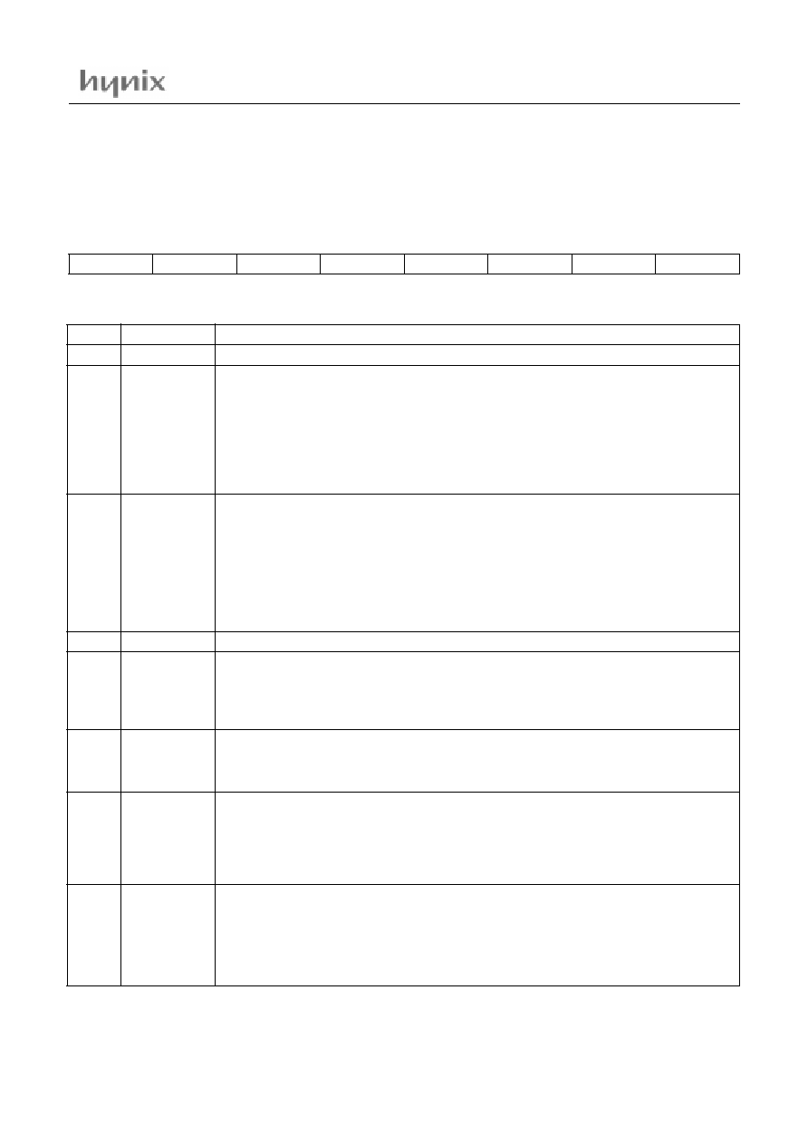
HMS91C7134
November.2001 ver1.0
43
16.1 The Special Function register for DDC Interface.
Eight SFR : S1CON, S1STA, S1DAT, S1ADR, RAMBUF, DDCCON, DDCADR, DDCDAT.
S1CON, S1STA, S1DAT, S1ADR are just the copies of the corresponding registers in general I2C-bus interface.
Table 16-1 DDC mode status and DDC1 control register (DDCCON : 0D7H) RESET VALUE:x00x0000B
Table 16-2 Description of the DDCCON bits
7
6
5
4
3
2
2
0
-
EX_DAT
SWENB
-
DDCINT
DDC1EN
SWHINT
M0
BIT
SYMBOL
FUNCTION
7
-
Reserved
6
EX_DAT
(R/W)
This bit defines the size of the EDID data. It is related to the function of the post increment of the
address pointer, DDCADR. When the upper limit is reached, the DDCADR will wrap around to
00H.
If EX_DAT is
1: The data size is 256 byte.
0: The data size is 128 byte(The addressing range for the EDID data buffer is mapped from 0 to
127 ; the rest, 128 to 255 , can still be used by the system).
5
SWENB
(R/W)
This bit indicates if the software/CPU is needed to take care of the operation of DDC1 protocol.
If SWENB is
1 : In DDC1 protocol, CPU is interrupted during the period of the 9th transmitting bit so that the
S/W service routine can update the hold register of transmitter by moving new data from appro-
priate area(it is not necessary to be the RAM buffer which is pointed by DDCADR) to the register
DDCDAT. This transmitting must be done within 40us.
0 : The hold register of the transmitter will be automatically updated from the RAM buffer without
the intervention of CPU.
4
-
Reserved
3
DDC1INT
(R/W)
Interrupt Request Bit. This bit is only valid in DDC1 protocol while S/W handling is enabled. This
bit is set by H/W and should be cleared by S/W in interrupt service routine.
1 : Interrupt request is pending.
0 : No interrupt request
2
DDC1EN
(R/W)
DDC1 enable control bit. If DDC1EN is
1 : DDC1 is enabled.
0 : DDC1 is disabled ; The activity on VSYNC is ignored.
1
SWHINT
(R/W)
Interrupt Request Bit. This bit is set by H/W when DDC interface switches from DDC1 to DDC2
(i.e. The voltage transient from high to low is observed on SCL1 pin). This bit should be cleared
by S/W in interrupt service routine.
1 : Interrupt request is pending.
0 : No interrupt request
0
M0
(R/W)
DDC mode indication bit. This bit will be set by H/W when the voltage transient from high to low
is observed on SCL1 pin. Once mode changes into DDC2 mode, the mode is reserved until pow-
er is off.
0: DDC1 is set.
1: DDC2 is set.

HMS91C7134
44
November.2001 ver1.0
DDC1 DATA register for transmission (DDCDAT : 0D5H)
· 8bit read and write register.
· Indicates DATA BYTE to be transmitted in DDC1 proto-
col.
Address pointer for DDC interface (DDCADR : 0D6H)
· 8bit read and write register.
· Address pointer with the capability of the post incre-
ment. After each access to RAMBUF register(either by
software or by hardware DDC1 interface), the content
of this register will be increased by one. It's available-
both in DDC1, DDC2 (DDC2B, DDC2B+, and DDC2AB)
and system operation.
Host type detection
The detection procedure conforms to the sequences proposed by
VESA Monitor Display Data Channel(DDC) specification.The
monitor needs to determine the type of host system:
· DDC1 or OLD type host.
· DDC2B host (Host is master, monitor is always slave)
· DDC2B+/DDC2AB(ACCESS.bus) host.
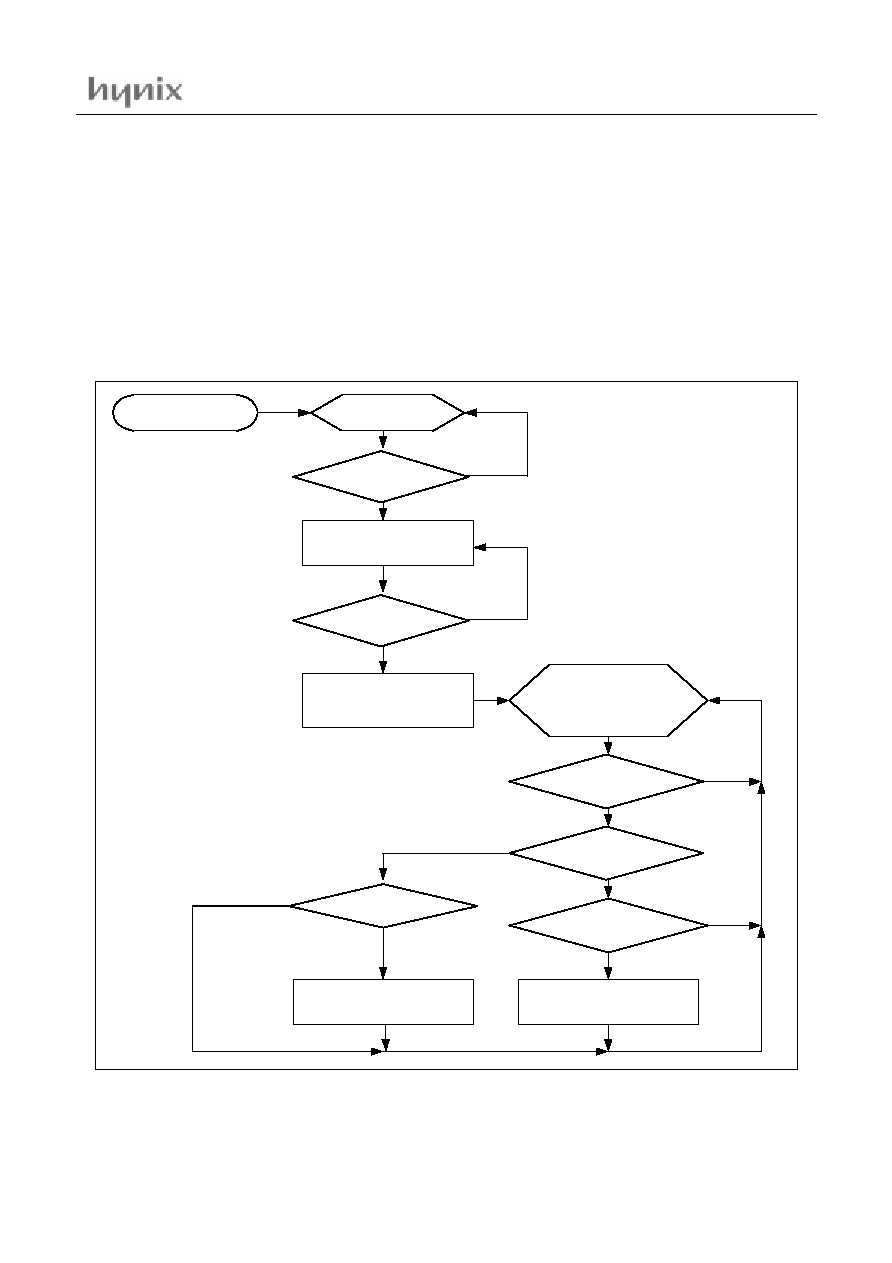
HMS91C7134
November.2001 ver1.0
45
The monitor where HMS9xC7134 resides is always both DDC1
and DDC2 capable with DDC2 having the higher priority. The-
display shall start transmitting DDC1 signals whenever it is pow-
ered on and the vertical sync signal is applied to it from the
hostfor the first time. The display shall switch to DDC2 within 3
system clocks as soon as it sees a high to low transition on the
clockline(SCL), indicating that there are DDC2 devices connect-
ed to the bus. Under that condition, the mode flag, M0 will be
changed from the default setting 0, to 1. Accordingly, the inter-
rupt will be invoked by setting flag, SWHINT as high.
Fig. 16.2 illustrates the concept and interaction between the mon-
itor and the host. After power on, the DDC1EN bit is set by S/W
to act as a DDC1 device. Therefore, the mode flag, M0, is set as
0. Following VSYNC as clock, the monitor will transmit EDID
data stream to the host. However, if DDC2 clock, SCL clock, is
present, the monitor will be switched to DDC2B device with the
mode flag setting as 1. Software will judge it is a DDC2B,
DDC2B+, or DDC2AB protocol.
Figure 16-2 Host type detection
Is VSYNC present ?
Has a command been received ?
Is 2B+/A.B command detected ?
Is monitor DDC2B+/DDC2AB
capable ?
Is command DDC2B command ?
Monitor Power on
Communication is idle
EDID sent continuously using
VSYNC as clock
Is DDC2 clock
present ?
Stop sending of EDID,
Switch to DDC2
communication mode
DDC2 communication
is idle. Monitor is
waiting for a command.
Respond to
DDC2B command
Respond to DDC2B+/
DDC2AB command
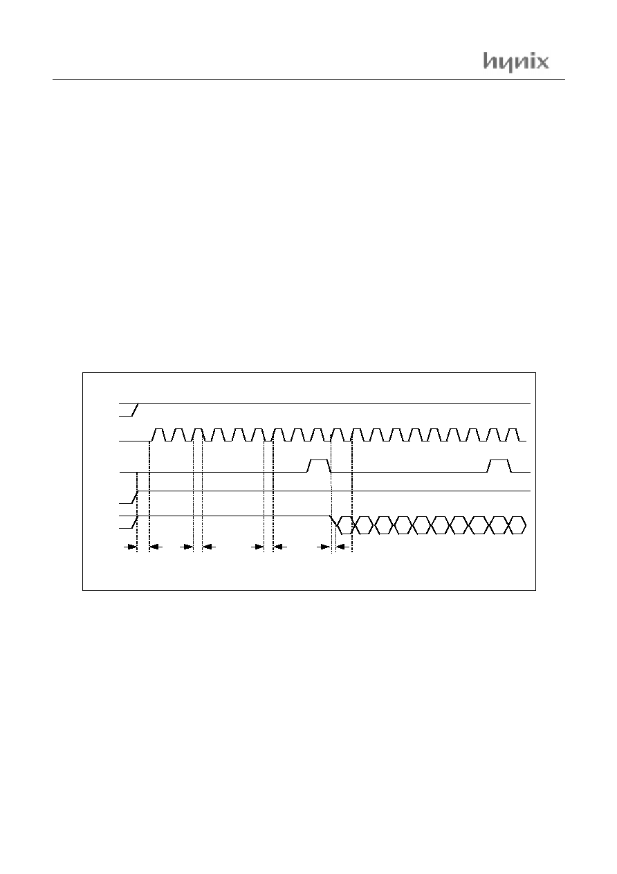
HMS91C7134
46
November.2001 ver1.0
16.2 DDC1 protocol
DDC1 is primitive and a point to point interface. The monitor is
always put at "Transmit only" mode.In the initialization phase, 9
clock cycles on VSYNC pin will be given for the internal syn-
chronization.During this period, the SDA pin will be kept at high
impedance state.
If DDC1 hardware mode is used, the following procedure is rec-
ommended to proceed DDC1 operation.
Step1 : Reset DDC1EN (by default, DDC1EN is cleared as low
after power on reset).
Step2 : Set SWENB as high(the default value is zero.)
Step3 : Depending on the data size of EDID data, set EX_DAT
as low(128 bytes) or high(256bytes).
Step4 : By using bulky moving commands (DDCADR, RAM-
BUF involved) to move the entire EDID data to RAM buffer.
Step5 : Reset SWENB to low.
Step6 : Reset DDCADR to 00H.
Step7 : Set DDC1EN as high.
In case SWENB is set as high, interrupt service routine must be
finished within 40 machine cycles in 12 MHz system clock.
Note : If EX_DAT equals to low, it is meant the lower part is oc-
cupied by DDC1 operation and the upper part is still free to
the system. Nevertheless, the effect of the post increment just ap-
plies to the part related to DDC1 operation.
In other words, the system program is still able to address the lo-
cations from 128 to 255 in the RAM buffer through MOVX com-
mand but without the facility of the post increment.
ex) In case of accessing 200 of the RAM Buffer.
MOV R0, #200
MOVX A, @R0
Figure 16-3 Transmission protocol in DDC1 interface.
16.3 DDC2B protocol
DDC2B is constructed base on Philips I2C interface. However, in
the level of DDC2B, PC host is fixed as the master and the mon-
itor is always regarded as the slave. Both master and slave can be
operated as a transmitter or receiver, but the master device deter-
mines which mode is activated. In this protocol, address pointer
is also used.
According to DDC2B specification, A0(for write mode) and
A1(for read mode) are assigned as the default address of moni-
tors.
The reception of the incoming data in write mode or the updating
of the outgoing data in read mode should be finished within the
specified time limit. If software in the slave
s side cannot react to
the master in time, based on I2C protocol, SCL pin can be
stretched low to inhibit the further action from the master. The
transaction can be proceeded in either byte or burst format.
1
2
3
4
5
6
7
8
9
1
2
3
4
5
6
7
8
9
1
B7 B6 B5 B4 B3 B2 B1 B0 HiZ B7
t
SU(DDC1)
t
DOV
Hi-Z
SCL
VCLK
DDC1INT
DDC1EN
SDA
t
H(VSYNC)
t
L(VSYNC)
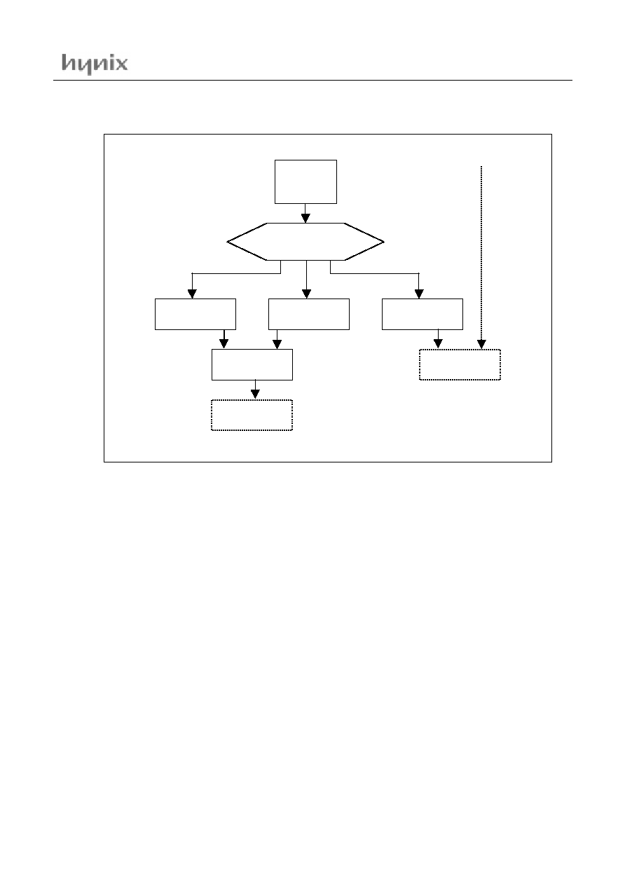
HMS91C7134
November.2001 ver1.0
47
Figure 16-4 The conceptual structure of DDC Interface
16.4 DDC2AB/DDC2B+ protocol
DDC2AB/DDC2B+ is a superset of DDC2B. Monitors that im-
plement DDC2AB/DDC2B+ are full featured ACCESS.bus de-
vices. Monitor that implement DDC2B+ uses the same command
set as DDC2AB but cannot use Access.bus device.
Essentially, they are similar to DDC2B. I2C interface forms the
fundamental layer for both protocols. The default address for
monitors is assigned as 6EH other than A0/A1H in DDC2B.
Monitors and hosts can play both the roles of master and slave.
Under this kind of protocol, it is easy to extend the support for
hosts to read VDIF(VESA Video Display Information Format)
and remotely control monitor functions.
Command / Information sequence between host and monitor
must conform to the specification of ACCESS.bus. Timing rules
specified in ACCESS.bus such as maximum response time to
RESET message(< 250 ms)form host, maximum time to hold
SCL low(< 2ms) etc. can be satisfied through software check and
built-in timers such as Timer0, Timer1.
In DDC2AB/DDC2B+, monitor itself can act as a monitor to ac-
tivate the transaction. The default address assigned for host is
50H.
DDC Interrupt
vector address
( 003BH )
DDC2B+/DDC2AB
Utilities
DDC2B
Utilities
DDC1
Utilities
Check Mode flag in DDCCON
Mode = 1 Mode = 1 Mode = 0
I2C
Service Routines
I2C Interface
(H/W)
DDC1 Transmitter
(H/W)
DDC2B+/DDC2AB
command received
DDC2B
command received
SWENB
= 1
SWENB
= 0

HMS91C7134
48
November.2001 ver1.0
16.5 The RAM Buffer and DDC application
RAM Buffer (RAMBUF) : the RAM buffer can be shared as the system RAM or DDC RAM buffer.
Table 16-3 Description of the EX_DAT and SWENB
Note
1. READ/WRITE through MOVX instruction might conflict with the access from DDC1 hardware. So, the access from
CPU by using MOVX instruction is forbidden.
2. READ/WRITE through DDCADR and RAMBUF registers has the conflicting problem also. Even the content of
DDCADR, which should be employed by DDC1 hardware, will be damaged. So, it is inhibited to use this type of access.
3. If DDCADR reaches 127, it will automatically wrap around to 0 after the access is done.
4. If DDCADR reaches 255, it will automatically wrap around to 0 after the access is done.
5. The access conflicting can be avoided because DDC1 access is done by the interrupt service routine. However, the EDID
transferring from the RAM buffer should be finished within 40 us.
MODE
EX_DAT
0
SWENB
0
DDC1
XRAM : 0 to 127
XRAM : 128 to 255
Normally reserved for DDC1
EDID data
(Note 1, Note 2, Note 3)
Available for the system
access.
(Note 2)
1
0
Normally reserved for DDC1
EDID data
(Note 1, Note 2)
Normally reserved for DDC1
EDID data.
(Note 1, Note 2, Note 4)
0
1
Normally reserved for DDC1
EDID data
(Note 3, Note 5)
Available for the system
access.
1
1
Normally reserved for DDC1
EDID data
(Note 5)
Normally reserved for DDC1
EDID data.
(Note 4, Note 5)
0
1
Normally reserved for DDC2
EDID data
(Note 3)
Available for the system
access.
1
1
Normally reserved for DDC2
EDID data
Normally reserved for DDC2
EDID data.
(Note 4)
DDC2

HMS91C7134
November.2001 ver1.0
49
Example Program; DDC Interface
Initial & Interrupt part
Initial:
mov DDCCON,#01h
; SWENB(0)
mov DDCADR,#0
;
mov DDCCON,#00100100b
; 128(6),DDC1_Int(5),DDC1_enable(1)
mov S1CON,#47h
; 100kHz(011),ENI1(1),ACK_enable(1)
mov S1ADR0, #0A1h
; DDC2B Slave address
mov S1ADR1, #41h
; Factory Alignment Host
;=================================================================
; DDC Interface
; 1. ISR
S1STA
�
S1DAT .
; 2. ISR
S1CON Refresh .
; 3. Slaver Receive Address match
! " S1DAT
�# S1STA
; Dummy Data
Writing$. % Slave Receive &'.
;=================================================================
; task
: DDC interrupt Service
; input
: Control & Status Peripheral register
;=================================================================
DDC_Header:
db
00,0FFh,0FFh,0FFh,0FFh,0FFh,0FFh,00
DDC_Isr:
push
PSW
;
push
DPH
;
push
DPL
;
push
ACC
;
push
00
;
push
01
;
mov
A, DDCCON
;
anl
A, #00001000b
; (1) DDC1INT request(bit3=1)?
jz
DDC2_svc
;
;=====================================================
DDC1_mode:
mov
A, mIICFlag
;
anl
A,#00000011b
;bUserSoftDDC(1), bDDC1Enable(0)
cjne
A, #03h, DDC1Enable
;
mov
A, #0FFh
;
mov
DDCDAT, A
;
ljmp
DDC_Int_end
;
DDC1Enable:
mov
A, mDDCData
;
mov
DDCDAT, A
;
mov
A, mDDCAddress
;
cjne
A, #80h, DDC1_Svc
;
mov
DDCCON, #01h
; DDC1 Disable,DDC2 Mode
DDC1_Svc:
clr
C
;
subb
A, #8
;
jnc
NormalDDC1
;
mov
DPTR, #DDC_Header
;
mov
A, R0
;
movc
A, @A+DPTR
;
sjmp
DDC1_Save
;
NormalDDC1:
mov
A, #EDID_DATA
;
add
A, R0
; data post
mov
R0, A
;
movx
A, @R0
;
DDC1_Save:
mov
DDCDAT, A
;
inc
mDDCAddress
;
ljmp
DDC_Int_end
;
;=====================================================
DDC2_svc:
mov
A, DDCCON
;
anl
A, #00000010b
; (2) SWHINT (SCLLow bit1=1) SCL activity ?
jz
DDC_I2C_svc
;
mov
mDDCAddress, #00h
; DDC1 Disable,DDC2 Mode
mov
DDCCON, #00000001b ;
DDC_I2C_svc:
mov
A, S1STA
; (3) i2C abnormal by G-call,Stop, Arbitration and no Acknowledge
mov
mI2C_status,A
;
anl
A, #11000110b
; 1 1 0 0 0 1 1 0
jnz
DDC_Abnormal
; GC,STOP,INTR,TX_MODE,BUSY,BLOST,/ACK_REP,SLV
mov
A, S1CON
;
anl
A, #00001000b
; (4) Host address matched ?
jnz
ADDR_Match
;
ljmp
DDC2B_svc
; (5) 1 byte data access by DDC2B format
Addr_Match:
mov
DDCCON, #01h
; DDC1 Disable,DDC2 Mode
setb
bI2C_Dir
; TX
mov
A, S1DAT
;
anl
A, #0FEh
; LSB BIT MASKING
cjne
A, #60h, DDC2B_mode ; 60h = Factory Host ?

HMS91C7134
50
November.2001 ver1.0
Factory_mode:
setb
bFactoryMode
; Factory Alignment Host matched 40h
setb
bService
;
mov
A, mI2C_status
;
anl
A, #10h
;
jz
Align_Add_Rx
; Slave Receive command
ljmp
Align_I2C_Tx
; Slave Transmit command
Align_Add_Rx:
clr
bI2C_Dir
; RX MCU <== Host
mov
A, #0
;
mov
mIICBuffer+pSave, A
;
mov
mIICBuffer+pRead, A
;
mov
S1DAT,#0FFh
; Dummy write
mov
S1CON, #01000111b
; i2C enable, Ack out when own slave address in
ljmp
DDC_Int_end
; Factory Slave Receive start
DDC2B_mode:
clr
bFactoryMode
; Factory Alignment Host matched
cjne
A, #0A0h, DDC_Abnormal; A0h = DDC2B Host ?
mov
A, mI2C_status
;
anl
A, #10h
;
jnz
DDC_I2C_Tx
; Slave Transmit
clr
bI2C_Dir
;
mov
S1DAT,#0FFh
; Dummy write
mov
S1CON, #01000111b
; i2C enable, Ack out when own slave address in
ljmp
DDC_Int_end
; DDC Slave Receive start
;=====================================================
DDC2B_svc:
; 1 byte data handling
jb
bFactoryMode,Line_svc ;
mov
A, mI2C_status
;
anl
A, #10h
;
jnz
DDC_I2C_Tx
; Slave Transmit
;
DDC_I2C_Rx:
mov
A, S1DAT
; Slave-Receive
mov
mDDCAddress, A
; subaddress catch
sjmp
DDC_I2C_ref
;
DDC_I2C_Tx:
mov
A, mDDCAddress
; Slave Transmit
anl
A, #7Fh
;
mov
R0,A
;
clr
C
;
subb
A, #8
;
mov
A, R0
;
jnc
Tx_mode_svc
;
mov
DPTR, #DDC_Header
; Header load
movc
A, @A+DPTR
;
sjmp Tx_Mode_out
;
Tx_mode_svc:
add
A, #EDID_DATA
; 0x80~0xFF
mov
R0, A
;
movx
A, @R0
;
Tx_Mode_out:
mov
S1DAT, A
; EDID data store at S1DAT
inc
mDDCAddress
;
mov
S1CON, #47h
; clear ADDR(bit3)11-15 edit
mov
nI2C_Abn_Cnt,#80h
; no Ack within 128 mSec, P1SFS.1=port
sjmp
DDC_Int_end
;
=====================================================
DDC_Abnormal:
mov
S1CON, #00000111b
; i2C enable, stop out, Ack out
mov
nI2C_Abn_Cnt,#0
; Initial hangup check counter
mov
P1SFS,#00001111b
; normal I2C hardware interface
clr
bFactoryMode
;
mov
DDCCON,#01h
; SWENB(0)
mov
DDCADR,#0
;
mov
DDCCON,#00100100b ; 128(6),DDC1_Int(5),DDC1_enable(1)
mov
S1CON,#47h
; 100kHz(011),ENI1(1),ACK_enable(1)
mov
S1ADR0, #0A1h
; DDC2B Slave address
mov
S1ADR1, #41h
; Factory Alignment Host
jnz
DDC_I2C_sTx
;
DDC_I2C_sRx:
;
mov
A,S1DAT
; Receive
sjmp
DDC_I2C_ref
;
DDC_I2C_sTx:
;
mov
S1DAT,#0FFh
; Transmit
DDC_I2C_ref:
;
mov
S1CON, #01000111b
; i2C enable, Ack out when own slave address in
;------------------------------------
DDC_Int_end:
pop
01
;
pop
00
;
pop
ACC
;
pop
DPL
;
pop
DPH
;
pop
PSW
;
reti
;
;------------------------------------
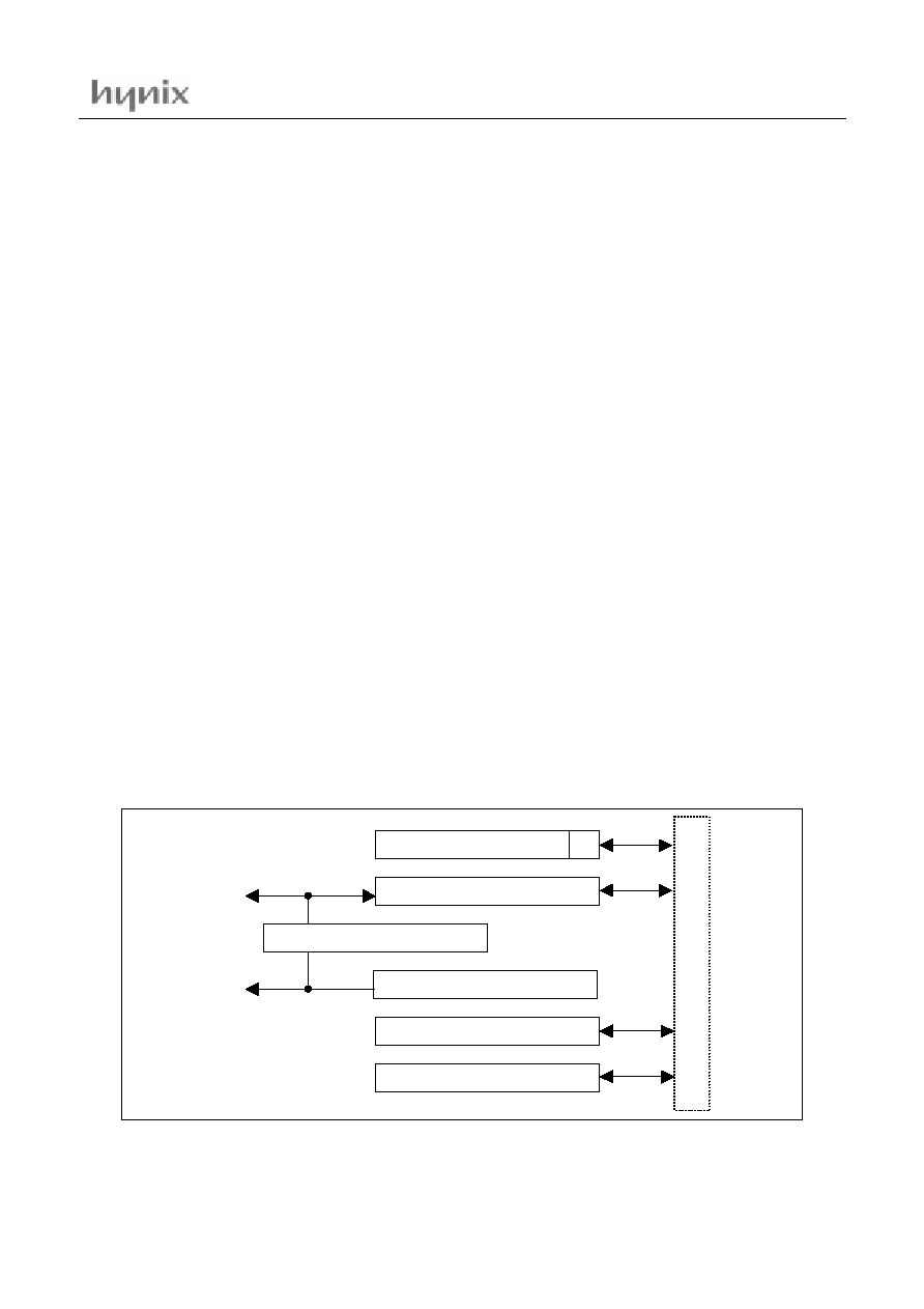
HMS91C7134
November.2001 ver1.0
51
17. I2C INTERFACE
In the Monitor MCU are two I2C interfaces implemented.
· The first one is used by the DDC protocols.
· The second one is dedicated for internal connection. With this one it
s possible to control the video, deflection, conver-
gence and some other functions of the monitor.
The serial port supports the twin line I2C-bus, consists of a data line(SDAx) and a clock line(SCLx).
· SDA1, SCL1 : the serial port line for DDC Protocol
· SDA2, SCL2 : the serial port line for Internal Connection
In both I2C interfaces, these lines also function as I/O port lines as follows.
· SDA1 / P1.1, SCL1 / P1.0, SDA2 / P1.7, SCL2 / P1.6
The system is unique because data transport, clock generation, address recognition and bus control arbitration are
all controlled by hardware.
The I2C serial I/O has complete autonomy in byte handling and operates in 4 modes.
· Master transmitter
· Master receiver
· Slave transmitter
· Slave receiver
These functions are controlled by the SFRs.
· SxCON : the control of byte handling and the operation of 4 mode.
· SxSTA : the contents of its register may also be used as a vector to various service routines.
· SxDAT : data shift register.
· SxADR : slave address register. Slave address recognition is performed by On-Chip H/W.
Figure 17-1 The block diagram of the I2C-bus serial I/O.
Slave Address
Shift Register
Arbitration + Sync. Logic
Bus Clock Generation
Control Register
Status Register
In
te
rn
a
l
B
u
s
SDAx
SCLx
-
7
0
0
0
0
7
7
7
HMS91C7134
52
November.2001 ver1.0
17.1 The Special Function register for I
2
C Interface.
Serial Control Register(SXCON; S1CON, S2CON)
Table 17-1 Serial control register(SxCON; S1CON : 0D8H , S2CON : 0DCH)
Table 17-2 Description of the SxCON bits
Table 17-3 Selection of the serial clock frequency SCL in Master mode of operation.
7
6
5
4
3
2
1
0
CR2
ENI1
STA
STO
ADDR
AA
CR1
CR0
BIT
7
SYMBOL
CR2
FUNCTION
This bit along with bits CR1and CR0 determines the serial clock frequency when
SIO is in the Master mode.
6
ENI1
Enable IIC. When ENI1 = 0, the IIC is disabled. SDA and SCL outputs are in the
high impedance state.
5
STA
START flag. When this bit is set, the SIO H/W checks the status of the I2C-bus
and generates a START condition if the bus free. If the bus is busy, the SIO will
generate a repeated START condition when this bit is set.
4
STO
STOP flag. With this bit set while in Master mode a STOP condition is
generated.
When a STOP condition is detected on the I2C-bus, the SIO hardware clears the
STO flag.
3
ADDR
This bit is set when address byte was received. Must be cleared by software.
2
AA
Acknowledge enable signal. If this bit is set, an acknowledge(low level to SDA)is
returned during the acknowledge clock pulse on the SCL line when :
·Own slave address is received
·A data byte is received while the device is programmed to be a Master Receiver
·A data byte is received while the device is a selected Slave Receiver. When this
bit is reset, no acknowledge is returned.
SIO release SDA line as high during the acknowledge clock pulse.
0
CR0
These two bits along with the CR2 bit determine the serial clock frequency when
SIO is in the Master mode.
1
CR1
CR2
CR1
f
osc
DIVISOR
BIT RATE (kHz) at f
osc
0
0
16
250
375
-
8MHz
12MHz
16MHz
CR0
0
0
0
14
285.71
428.57
-
1
0
1
40
100
150
-
0
0
1
60
66.67
100
-
1
1
0
120
33.33
50
-
0
HMS91C7134
November.2001 ver1.0
53
Serial Status Register(SXSTA)
SxSTA is a read-only register. The contents of this register may be used as a vector to a service routine. This optimized the response
time of the software and consequently that of the I2C-bus. The status codes for all possible modes of the I2C-bus interface are given
Table
Table 17-4 Serial status register
(SXSTA; S1STA:0D9H, S2STA:0DDH)
Table 17-5 Description of SxSTA
Data Shift Register(SXDAT; S1DAT, S2DAT)
SxDAT contains the serial data to be transmitted or data which has just been received. The MSB (bit7) is transmitted or
received first; I,e. data shifted from right to left.
Table 17-6 Serial data shift register
Addressing Register(SXADR)
This 8-bit register may be loaded with the 7-bit slave address to which the controller will respond when programmed as a slave receive/
transmitter.
Table 17-7 Address register(SLA6 to SLA0 : Own slave address.)
7
6
5
4
3
2
1
0
GC
STOP
INTR
TX_MODE
BBUSY
BLOST
/ACK_REP
SLV
BIT
7
SYMBOL
GC
FUNCTION
General Call flag.
6
STOP
STOP flag.
This bit is set when a STOP condition was received.
5
INTR
Bus busy state flag.
This bit is set when the bus is being used by another master. Otherwise, this bit is reset.
Interrupt flag.
This bit is set when a SIO interrupt is requested.
4
TX_MODE
Transmission mode flag.
This bit is set when the SIO is a transmitter. Otherwise, this bit is reset.
Bus lost flag.
This bit is set when the master loses the bus contention. Otherwise, this bit is reset.
1
/ACK_REP
Acknowledge response flag.
This bit is set when the receiver transmits the not acknowledge signal.
This bit is reset when the receiver transmits the acknowledge signal.
Slave mode flag.
This bit is set when the SIO plays role in the slave mode. Otherwise, this bit is reset.
BLOST
2
SLV
0
BBUSY
3
7
6
5
4
3
2
1
0
SxDAT7
SxDAT6
SxDAT5
SxDAT4
SxDAT3
SxDAT2
SxDAT1
SxDAT0
7
6
5
4
3
2
1
0
SLA6
SLA5
SLA4
SLA3
SLA2
SLA1
SLA0
-

HMS91C7134
54
November.2001 ver1.0
17.2 Programmer's Guide for I2C and DDC2
The I2C serial I/O and DDC Interface has operates in 4 modes.
· Master transmitter
· Master receiver
· Slave transmitter
· Slave receiver
17.2.1 Master transmitter mode
Slave transmitter mode
1. Read SxSTA.
2. If BBUSY == 1 then
go to step1.
Else then
write slave address to SxDAT and set both ENI and STA, reset AA in SxCON.
3. Wait for interrupt.
4. Read SxSTA.
If BLOST == 1 or /ACK_REP == 1* then
write dummy data to SxDAT.
Go to step1.
Else then
clear STA.
5. Perform required service routines.
If this datum == LAST then
set STO in SxCON and write last data to SxDAT**.
Go to step 6.
Else then
write next data to SxDAT**.
Go to step3.
6. Wait for interrupt.
Write dummy data to SxDAT**.
* : 1. If the master don't receive the acknowledge from the slave, it generates the STOP condition and returns to the IDLE state.
**: 1. This action should be the last in service routine.
1. Write slave address to SxADR, set AA and ENI in SxCON.
2. Wait for interrupt.
3. Read SxSTA and write the first data to SxDAT*. Reset AA in SxCON.
5. Wait for interrupt.
6. Read SxSTA.
If /ACK_REP == 1** then
Go to step7.
Else then
write the next SxDAT*.
Go to step5.
7. Write dummy data to SxDAT*.
* : 1. These actions should be the last.
**: 1. If the master want to stop the current data requests, it don't have to acknowledge to the slave transmitter.
2. If the slave don't receive the acknowledge from the master, it releases the SDA and enters the IDLE state,
so if the master is to resume the data requests, it must regenerate the START condition.

HMS91C7134
November.2001 ver1.0
55
Master receiver mode
Slave transmitter mode
1. Read SxSTA.
2. If BBUSY == 1 then
go to step1.
Else then
write slave address to SxDAT and set both ENI1 and STA, reset AA in SxCON.
3. Wait for interrupt.
4. Read SxSTA.
If BLOST == 1 or /ACK_REP == 1 then
write dummy data to SxDAT
Go to step1.
Else then
clear STA and write FFH to SxDAT.
Set AA in SxCON.
5. Wait for interrupt.
6. Read SxSTA.
If this datum == LAST then
reset AA* and read SxDAT**.
Go to step7.
Else then
read SxDAT**.
Go to step5.
7. Wait for interrupt.
Read SxSTA.
Read SxDAT**.
* : 1. If the master want to terminate the current data requests, it don't have to acknowledge to the slave.
**: 1. This action should be the last.
1. Write slave address to SxADR, set AA and ENI in SxCON.
2. Wait for interrupt.
3. Read SxSTA and write FFH to SxDAT*.
5. Wait for interrupt.
6. Read SxSTA.
If STOP == 1 then
Go to step7.
Else then
read data from SxDAT*.
Go to step5.
7. Read dummy data from SxDAT*.
* : 1. This action should be the last.

HMS91C7134
56
November.2001 ver1.0
Master : restart (transmitter)
1. Read SxSTA.
2. If BBUSY == 1 then
go to step1.
Else then
write slave address to SxDAT and set both ENI1 and STA in SxCON.
Reset AA in SxCON.
3. Wait for interrupt.
4. Read SxSTA.
If BLOST == 1 or /ACK_REP == 1 then
write dummy data to SxDAT.
Go to step1.
Else then
clear STA.
5. Perform required service routines.
If this datum == LAST then
if RESTART is required then
set STA in SxCON and write last data to SxDAT*.
Go to step6.
Else then
set STO in SxCON and write last data to SxDAT*.
Go to step7.
Else then
write next data to SxDAT*.
Go to step3.
6. Wait for interrupt.
Write slave address to SxDAT*.
Go to step3.
7. Wait for interrupt.
Write dummy data to SxDAT*.
* : 1. This action should be the last in service routine.
HMS91C7134
November.2001 ver1.0
57
18. PULSE WIDTH MODULATION
18.1 Static PWM
There are eight static PWM in the HMS9xC7134.
These channels provide output pulses of programmable duty cy-
cle and polarity. The duty cycle is defined by a counter.
The 8-bit counter of a PWM counts modulo 256, i.e. from 0 to
255 inclusive. The value held in the 8-bit counter is compared to
the contents of the Special Function Register(PWMn) of the cor-
responding PWM. The polarity of the PWM outputs is program-
mable and selected by the PWMLVL bit in PWMCON register.
Provided the contents of a PWMn register is equal to or greater
than the counter value, the corresponding PWM output is set
HIGH (with PWMLVL ="0"). If the contents of this register is
less than the counter value, the corresponding PWM output is set
LOW(with PWMLVL ="0"). The pulse-width-ratio is therefore
defined by the contents of the corresponding Special Function
Register(PWMn) of a PWM. By loading the corresponding Spe-
cial Function Register(PWMn) with either 00H or FFH, the
PWM output can be retained at a constant HIGH or LOW level
respectively(with PWMLVL = "0").
The PWM outputs PWM0 to PWM7 register share the same pins
as Port2.2~Port2.7, Port3.4 and Port3.5 respectively.
Selection of the pin function as either a PWM output, a Port line
or the other function is achieved by using the appropriate value of
P2SF register.
The repetition frequency (fPWM) at a PWM output is given by:
fPWM = fOSC / (2 x 256)
Table 18-1 PWM control register (PWMCON : 0A1H)
Table 18-2 Description of the PWMCON bits
7
6
5
4
3
2
1
0
PWMLVL
PWM6CFG
PWM5CFG
PWM4CFG
PWM3CFG
PWM2CFG
PWM1CFG
PWM0CFG
BIT
SYMBOL
FUNCTION
7
PWMLVL
Polarity selection of the PWMs.
0 : PWM outputs are not inverted.
1 : PWM outputs are inverted.
6 to 0
PWM6CFG to
PWM0CFG
Output type selection of the PWMs.
0 : open-drain type.
1 : push-pull type
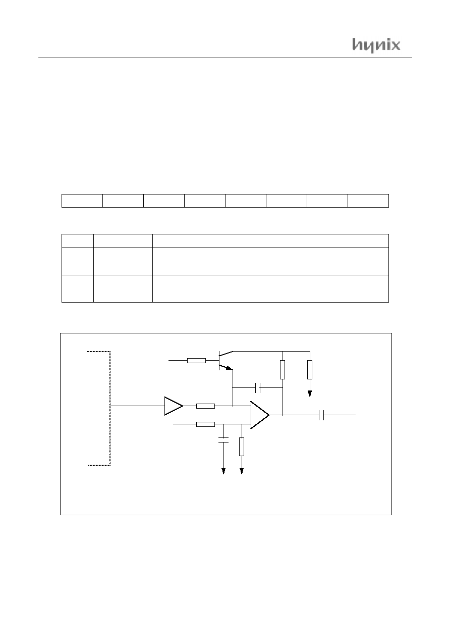
HMS91C7134
58
November.2001 ver1.0
18.2 Dynamic PWM
There are two dynamic PWMs in the HMS9xC7134. The DP-
WMs can be used to generate various waveform by software pro-
gramming, and are used to achieve geometric compensation by
generating a parabola output waveform which is synchronized
with VSYNCin signal for pin/trap, bow/tilt, vertical linearity or
focus compensation in monitor system.
This is achieved by utilizing timer2. The low 8-bit in timer2 is
used as 8-bit counter for PWM signal and the high 8-bit in timer2
is used to decide the number of PWMs in one video frame. One
video frame can be divided to any number of blocks according to
the register RC2H value within 256 blocks, and here the RC2L
will be 00H for 8-bit PWM resolution.
The dynamic PWM outputs DPWM0 to DPWM1 register share
the same pins as Port2.0~Port2.1respectively.
The repetition frequency (fDPWM) at a DPWM output is given
by (in case of RC2L=00H): fDPWM = fOSC / (2 x 256)
Table 18-3 Dynamic PWM control register (DPWMCON : 0B1H)
Table 18-4 Description of the DPWMCON bits
Table 18-5 DPWM application circuit
7
6
5
4
3
2
1
0
DPWMLVL
-
-
-
-
-
DPWM1CFG DPWM0CFG
BIT
SYMBOL
FUNCTION
7
DPWMLVL
Polarity selection of the DPWMs.
0 : DPWM outputs are not inverted.
1 : DPWM outputs are inverted.
1 to 0
DPWM1CFG to
DPWM0CFG
Output type selection of the DPWMs.
0 : open-drain type.
1 : push-pull type
DPWMx
Vsync
VDD
HMS91C7134
November.2001 ver1.0
59
Using one Dynamic PWM to compensate the following H size distortion :
Using one Dynamic PWM to compensate the following H center distortion :
1. Pincushion (PCC amplitude)
2. Trapezoid (Keystone)
3. CBOW (Quarter Width)
4. PCC corner
5. S Curve
1. Pin Balance (Bow)
2. Key Balance (Tilt)
3. Corner Balance
HMS91C7134
60
November.2001 ver1.0
19. SYNC PROCESSOR
The characteristics of Sync processor are as follows.
Automatic mode detection by hardware to capture the following signal characteristics :
· Hsync and Vsync frequency measured with 12-bit accuracy (fSH= 12MHz, fSV= 125KHz)
· Hsync and Vsync polarity
· Hsync and Vsync presence needed for implementing the VESA DPMS standard
Integrated composite sync separation
Integrated signal generators for generating :
· Free running horizontal and vertical sync pulses
· Clamping pulse(Back porch, Front porch)
· Pattern signal (white picture, black picture, cross hatch and inverse cross hatch)
Special option :
· Missing sync pulse insertion
All measured parameters are stored in Special Function Register such that the data is available at any time.
The block diagram of the complete sync processor is given in Figure 19-1
19.1 Sync input signals
The sync inputs are able to handle standard TTL level sync sig-
nals. From Figure 19-1 it can be seen that both the HSYNCin and
SOGin inputs accept composite sync signals. The HSYNCin and
VSYNCin input is meant to be connected to the Hsync and Vsync
of the VGA cable while SOGin input is meant to be connected to
a sync slicer in order to handle Sync-On-Green at the video input.
This last signal should have a TTL level also. The selection be-
tween the HSYNCin and the SOGin inputs, as well as the selec-
tion between the VSYNCin and separated Vsync, can be done via
software.
Table 19-1 Sync Input selection
19.2 Horizontal polarity correction
In order to simplify the processing in the following stages, the
HSYNC polarity correction circuit is able to convert the input
sync signals to positive polarity signals in all situations. This cor-
rection is achieved by the aid of HPOL and HP.
HPOL and HP are only settled down in several horizontal scan-
ning lines or a few milliseconds after power-on or timing mode
change.
19.3 Vertical polarity correction
The purpose of the vertical polarity correction is similar to the
horizontal polarity correction. To get the correct resultafter pow-
er-on or a timing mode change, at least 5 frames is needed.
19.4 Vertical sync separation
This block separates the vertical sync from a composite sync sig-
nal. At approximately 1/4 of each HSYNC line the logical level
is latched. This yields a slightly delayed vertical sync signal.
Special precautions have been taken to suppress equalizing puls-
es when present and to allow both polarities of the composite sig-
nal.The format of the composite sync signal can be standard, as
given in Figure 19-2, or can be one of the non standard format as
given in Figure 19-3
Select Flag
HSEL
Signal to detector
0 : HSYNCin
1 : SOGin
VSEL
0 : VSYNCin
1 : Separated VSYNC
HMS91C7134
November.2001 ver1.0
61
Figure 19-1 Block diagram of sync processor
CA
P
T
U
R
E
SFR
CO
N
T
R
O
L
SFR
1 / 96
f
SH
f
SV
f
OS
C
HP
VP
HP
O
L
VP
O
L
HP
RE
S
V
P
R
E
S
HS
Y
N
C
C
h
a
nge
VS
Y
N
C
C
h
a
nge
C
P
U
M
DINT
CP
U
HF
VF
CONT
R
O
L
VINT
MU
X
XOR
SYNC
SEP
HSYNC
DE
T
E
C
T
ION
HSYNC
GE
NE
R
A
T
O
R
VSYNC
DE
T
E
C
T
ION
VSYNC
GE
NE
R
A
T
O
R
MU
X
/
CL
M
P
V
H
HP
HSYNC
out
CL
A
M
P
VSYNC
out
HP
HP
O
L
HP
RES
VP
VP
O
L
VP
RE
S
HP
HF
HOP
OL
HP
G
HOP
W
VP
VF
VOP
OL
VP
G
VOP
W
HSE
L
VSE
L
HSYNC
i
n
SOGin
VSYNC
i
n
HPOL
VPOL
PAT
O
UT
PA
T
MU
X
MU
X
XOR
HMS91C7134
62
November.2001 ver1.0
19.5 Horizontal sync. detection
This block extracts the following parameters from the incoming
horizontal or composite sync :
· HPER : The number of clock cycles (fSH = 12MHz) be-
tween five sync pulses (4 period time), thus the 12 bits val-
ue HPER will be equal to ((4 x 12 x 106 / fH) - 1) where fH
is the horizontal sync frequency in Hz.
· HPOL : The polarity of the sync signal, HPOL will be reset
in case of a positive polarity and set in case of a negative
polarity. The 1/4 point value of HSYNC period time will be
latched for HPOL.
· HPRES :To detect the presence of the valid HSYNC sig-
nal, Detector measures the time interval between five sync
pulses (4 period time). No active sync is coming in if the
counter reaches a value of FF0H(4080).
· HCHG : The HCHG flag will be set if a change is detected
in either the polarity or the period time. To avoid unintended
setting of the HCHG flag a small deviation in the period time
is allowed.The allowed deviation is approximately 167ns
per line.
19.6 Vertical sync. detection
This block extracts the following parameters from the incoming
vertical sync:
· VPER : Either the number of clock cycles (fSV=125kHz
sampling) between two sync pulses(period time). In case
the period time is measured this 12 bits VPER will be equal
to 125 x 103 / fV where fV is the vertical sync frequency in
Hz.
· VPOL : The polarity of the sync signal, VPOL will be reset
in case of a positive polarity and reset in case of a negative
polarity. It should be noted here that in case of a composite
sync signal at the input the parameter VPOL will be set al-
ways, disregarding the polarity of the incoming composite
sync. The 1/4 value of incoming VSYNC value will be
latched for VPOL.
· VPRES : To detect the presence of the valid VSYNC sig-
nal, Detector measures the time interval between two con-
secutive rising edges of the input signal. No active sync is
coming in if the counter reaches a value of FF0H(4080).
· VCHG : The VCHG flag will be set if a change is detected
in either the polarity or the period time. To avoid unintended
setting of the VCHG flag a small deviation in the period
time is allowed.The allowed deviation is approximately
32us per line.
Table 19-2 Threshold frequencies of the presence detector
Detection input
Threshold frequency
HSYNC input
12 KHz
VSYNC input
30 Hz
HMS91C7134
November.2001 ver1.0
63
Figure 19-2 Standard composite sync signals
Figure 19-3 Non-standard composite sync signals
CSYNC
HSYNC
VSYNC
2nd field
1st field
CSYNC
HSYNC
VSYNC
1st field
2nd field
HSYNC
VSYNC
CSYNC-1
CSYNC-2
CSYNC-3
CSYNC-4
CSYNC-5
CSYNC-6
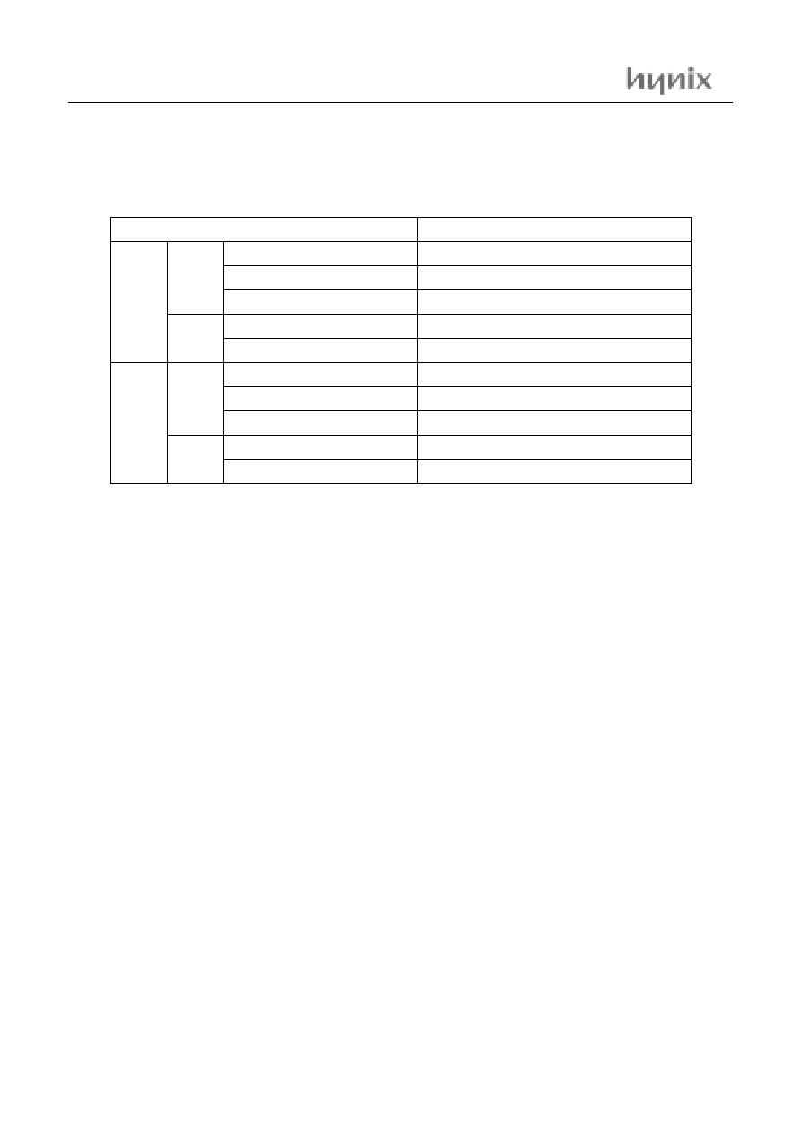
HMS91C7134
64
November.2001 ver1.0
Both the HCHG and the VCHG signals are combined and con-
nected to the internal interrupt. Interrupt will be issued when
change is continuously detected like following table.
Due to this fast interrupt the S-correction can be set to a safe level
before any damage to the deflection circuitry will occur.
Table 19-3 Time interval between mode change and interrupt
Internally there are two 12-bit counter for HSYNC and VSYNC
period check , HSYNC counter count up from 0 to 4096 for 4
HSYNC lines according to 12MHz clock, and VSYNC counter
count up from 0 to 4096 for one VSYNC line according to
125KHz clock. For HSYNC static state that HSYNC frequency
is under 12KHz, counter value is more than 4080 value,and for
VSYNC static state that VSYNC frequency is under 32Hz,
counter value is more than 4080 value.
HSYNC
HPnew < HPpre
HPnew x 61 to (4 x HPnew x 15) - (n x HPpre)
HPnew > HPpre
(4 x HPnew) x 3 - (n x HPpre)
POS => NEG
60 HSYNC lines
NEG => POS
60 HSYNC lines
VSYNC
Period
Period
Polarity
Polarity
VPnew < VPpre
(VPnew x 2 + VPprev) to (Vnew x 3)
VPnew > VPpre
(VPnew) to (VPnew x 2)
POS => NEG
3 VSYNC lines
NEG => POS
2 VSYNC lines
Mode change
Interval between mode change and interrupt
To Static State
(4 x HPnew) x 3 - (n x HPpre)
To Static State
(VPnew) to (VPnew x 2)
HMS91C7134
November.2001 ver1.0
65
19.7 Horizontal sync. generator
This block generates horizontal sync pulses with positive polari-
ty.This can be done in 3 modes, selectable with HPG. When HPG
is 00, the generator operates in the free running mode and the gen-
erated pulse repetition period equals HF x 1/12 MHz clock peri-
od, where HF is a 10 bit value. As a result the frequency of the
free running output sync pulse equals 12 x 106 / HF, with about
12 kHz as lower boundary.When HPG is 01, the input sync pulse
is followed and a substitution pulse is inserted. In case HPG
equals 11, the inputsync pulse is followed but a substitution pulse
is disabled, while the incoming sync is missing.
Table 19-4 Modes of the horizontal pulse generator
Table 19-5 Free running horizontal sync pulse width
Example Program; Freerun mode
HPG[1:0]
Selected mode
0 0
Free running mode
Period time of horizontal pulse generator (= HF)
0 1
The same pulse as the input horizontal sync
Substitution pulse insertion in case of a missing sync pulse
1 0
Reserved
1 1
The same pulse as the input horizontal sync
No substitution pulse insertion in case of a missing sync pulse
HOPW[4:0]
Selected mode
00000
2 x 83 ns
00001
3 x 83 ns
00010
4 x 83 ns
-------
Incremented by 83ns (1/12 x 10
-6
)
11101
31 x 83 ns
11110
32 x 83 ns
11111
33 x 83 ns
;================================================================
;
Free running
;================================================================
SetFreeRunning:
lcall
SetVcp
SetFreeRunning1:
mov
A, #01000100b
; rising Edge Interrupt
mov
MDCON, A
;
mov
HFH,#00101110b
; Hf = 64.6 kHz
mov
HFL,#01010000b
; HOPW[10000]
mov
VFH,#01000010b
; Vf = 60 Hz
mov
VFL,#11001000b
; VOPW[1000]
mov
CPGEN,#11100000b
; White Picture Clamping and Pattern
mov
A, #01000000b
; Negative Hsync, Positive Vsync free-run
mov
HVGEN, A
;
lcall
DpmsHLinearity
;
ret
HMS91C7134
66
November.2001 ver1.0
19.8 Vertical sync. generator
This block generates vertical sync pulses with positive polarity.
This can be done in 3 modes, selectable with VPG. When VPG is
00, the generator operates in the free running mode and the gen-
erated pulse repetition period equals VF x HF x 1/12 MHz clock
period, where VF is a 12 bit value. As a result the frequency of
the free running output sync pulse equals 12 x 106 / HF / VF.
When VPG is 01, the input sync pulse is followed and a substitu-
tion pulse is inserted. In case VPG equals 11, the input sync pulse
is followed but a substitution pulse is disabled, while the incom-
ing sync is missing.
Table 19-6 Modes of the vertical pulse generator
Table 19-7 Free running vertical sync pulse width
19.9 HSYNC / VSYNC output driver
This is output stage for HSYNCout and VSYNCout. It offers out-
put selection, output enabling/disabling and output polarity selec-
tion. With HOPOL and VOPOL the output is selected.
VPG[1:0]
Selected mode
0 0
Free running mode
Period time of vertical pulse generator (= VF)
0 1
The same pulse as the input horizontal sync
Substitution pulse insertion in case of a missing sync pulse
1 0
Reserved
1 1
The same pulse as the input vertical sync
No substitution pulse insertion in case of a missing sync pulse
VOPW[3:0]
Selected mode
0000
2 x t
H(free)
0001
3 x t
H(free)
0010
4 x t
H(free)
-------
Incremented by t
H(free)
1101
15 x t
H(free)
1110
16 x t
H(free)
1111
17 x t
H(free)
HMS91C7134
November.2001 ver1.0
67
19.10 Clamp pulse generator
The clamp pulse is generated by setting CLMPEN and always ac-
companies the HSYNCout pulse, even in the free running mode.
This block generates a clamping pulse with programmable pulse
width, determined by CPW. It can be started at the front porch
(CFB reset) or at the back porch (CFB set), and the polarity can
be set with COPOL.
Table 19-8 Clamping pulse width
19.11 Pattern generator
This generator is used for test pattern generation when in free run-
ning mode.Four picture can be selected : a white, a cross hatch, a
balck and inverted cross hatch pictures.When not in free running
mode , the output is disabled. The pattern output can be used for
burn-in test or e.g. for quick servicing without the need of a video
source. The displayed pattern might look different in the different
timing modes,symmetric display is not guaranteed.
19.12 Suspend mode
The complete Sync processor can be set into a suspend mode for lowering the power consumption by means of signal MDDN.
Table 19-9 Suspend mode
Table 19-10 Mode detection control register.(MDCON : 0F1H)
CPW[2:0]
Clamping pulse width
000(11)
5 x 83ns
001(11)
9 x 83ns
010(11)
13 x 83ns
011(11)
17 x 83ns
100(11)
21 x 83ns
101(11)
25 x 83ns
110(11)
29 x 83ns
111(11)
33 x 83ns
MDDN
Mode
0
Sync. processor is running.(default)
1
Sync. processor is disabled.
7
6
5
4
3
2
1
0
MDDN
CLMPEN
PATEN
-
-
VINTE
HSEL
VSEL
HMS91C7134
68
November.2001 ver1.0
Table 19-11 Description of the MDCON bits
Table 19-12 Mode detection status register(MDST : 0F2H)
Table 19-13 Description of the MDST bits
BIT
SYMBOL
FUNCTION
7
MDDN
0 : hardware mode detection operating normally(default)
1 : hardware mode detection disabled (low power consumption)
4 to 3
-
Not used
1
HSEL
0 : VSYNCin
1 : separated VSYNC
0
VSEL
0 : HSYNCin
1 : SOGin
2
VINTE
Vsync rising or falling edge interrupt select
0: Vsync rising edge interrupt
1: Vsync falling edge interrupt
6
CLMPEN
0 : clamp pulse out disabled(default)
1 : clamp pulse out enabled
5
PATEN
0 : pattern out disabled(default)
1 : pattern out enabled
7
6
5
4
3
2
1
0
-
VINT
HPRES
VPRES
HPOL
VPOL
HCHG
VCHG
BIT
SYMBOL
FUNCTION
5
HPRES
Indicate the presence of Hsync
0 : not present (Hfreq < 12 kHz)
1 : present ( Hfreq
12 kHz)
4
VPRES
Indicate the presence of Vsync
0 : not present (Vfreq < 30 Hz)
1 : present ( Vfreq
30 Hz)
3
HPOL
Indicate the polarity of Hsync/Csync :
0 : positive polarity
1 : negative polarity
2
VPOL
Indicate the polarity of Vsync :
0 : positive polarity
1 : negative polarity
6
VINT
Vsync interrupt flag
7
-
Not used
1
HCHG
Indicate a change in horizontal period and/or polarity:
0 : no change
1 : change detected
0
VCHG
Indicate a change in vertical period and/or polarity:
0 : no change
1 : change detected
HMS91C7134
November.2001 ver1.0
69
Table 19-14 Vsync period low byte register (VPH : 0F3H)
Table 19-15 Hsync period low byte register (HPH : 0F4H)
Table 19-16 Vsync and Hsync period low high register (VHPL : 0F5H)
Table 19-17 Hsync and Vsync generation control register.(HVGEN : 0F9H)
Table 19-18 Description of the HVGEN bits
7
6
5
4
3
2
1
0
VP11
VP10
VP9
VP8
VP7
VP6
VP5
VP4
7
6
5
4
3
2
1
0
HP11
HP10
HP9
HP8
HP7
HP6
HP5
HP4
7
6
5
4
3
2
1
0
VP3
VP2
VP1
VP0
HP3
HP2
HP1
HP0
7
6
5
4
3
2
1
0
-
HOPOL
HPG1
HPG0
-
VOPOL
VPG1
VPG0
BIT
SYMBOL
FUNCTION
6
HOPOL
Select polarity of the horizontal output pulse
0 : positive polarity
1 : negative polarity
7
-
Not used
5 to 4
HPG1
to
HPG0
Horizontal pulse output modes
00 : free running
01 : missing insertion
10 : reserved
11 : the same pulse as the incoming horizontal sync.
2
VOPOL
Select polarity of the vertical output pulse
0 : positive polarity
1 : negative polarity
1 to 0
VPG1
to
VPG0
Vertical pulse output modes
00 : free running
01 : missing insertion
10 : reserved
11 : the same pulse as the incoming vertical sync.
3
-
Not used
HMS91C7134
70
November.2001 ver1.0
Table 19-19 Vsync free running output high byte register (VFH : 0FBH)
Table 19-20 Vsync free running output low byte register (VFL : 0FCH)
Table 19-21 Hsync free running output high byte register (HFH : 0FDH)
Table 19-22 Hsync free running output low byte register (HFL : 0FEH)
Table 19-23 Clamping and Pattern control register(CPGEN : 0FAH)
Table 19-24 Description of the CPGEN bits
7
6
5
4
3
2
1
0
VF11
VF10
VF9
VF8
VF7
VF6
VF5
VF4
7
6
5
4
3
2
1
0
VF3
VF2
VF1
VF0
VOPW3
VOPW2
VOPW1
VOPW0
7
6
5
4
3
2
1
0
HF9
HF8
HF7
HF6
HF5
HF4
HF3
HF2
7
6
5
4
3
2
1
0
HF1
HF0
-
HOPW4
HOPW3
HOPW2
HOPW1
HOPW0
7
6
5
4
3
2
1
0
COPOL
CFB
CPW2
CPW1
CPW0
-
PATS1
PATS0
BIT
SYMBOL
FUNCTION
7
COPOL
Select the polarity or level of the clamping pulse:
0 : positive polarity when enabled, static low level when disabled
1 : negative polarity when enabled, static high level when disabled
6
CFB
Select the trigger moment of the clamping output pulse :
0 : clamp pulse after FRONT porch of horizontal sync
1 : clamp pulse after BACK porch of horizontal sync
5 to 3
CPW2 to CPW0
Clamp pulse width
1 to 0
PATS1 to PATS0
Select one of the following patterns :
00 : white picture
01 : cross hatch picture
10 : black picture
11 : inverse cross hatch picture
2
-
Not used
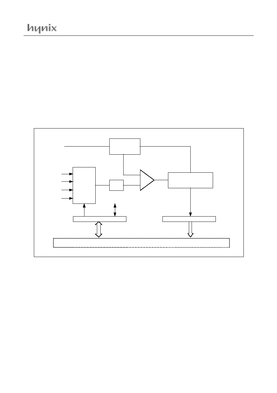
HMS91C7134
November.2001 ver1.0
71
20. ANALOG-TO-DIGITAL CONVERTOR (ADC)
The analog to digital converter (A/D) allows conversion of an an-
alog input to a corresponding 8-bit digital value. TheA/D module
has four analog inputs, which are multiplexed into one sample
and hold. The output of the sample and hold is the input into the
converter, which generates the result via successive approxima-
tion. The analog supply voltage is connected to VDD2 of ladder
resistance of A/D module.
The A/D module has two registers which are the control register
ACON and A/D result register ADAT. The register ACON,
shown in Table 17.1, controls the operation of the A/D converter
module. To use analog inputs, I/O is selected by P1SFS register.
The processing of conversion starts when the start bit ADST is set
to "1". After one cycle, it is cleared by hardware. The register
ADAT contains the results of the A/D conversion. When conver-
sion is completed, the result is loaded into the ADAT the A/D
conversion status bit ADSF is set to "1".
The block diagram of the A/D module is shown in Fig. 17.1. The
A/D status bit ADSF is set automatically when A/D conversion is
completed, cleared when A/D conversion is in process. The con-
version time takes maximum 13us (@12MHz)
Figure 20-1 A/D block diagram
Input
MUX
ACH0
ACH1
ACH2
ACH3
ACON
INTERNAL BUS
ADAT
VDD2
Ladder
Resistor
Decoder
S/H
Successive
Approximation
Circuit
HMS91C7134
72
November.2001 ver1.0
Table 20-1 ADC control register (ACON : 97H)
Table 20-2 Description of the ACON bits
Table 20-3 ADC data register (ADAT : 96H)
Table 20-4 Description of the ADAT bits
7
6
5
4
3
2
1
0
-
-
ADEN
-
ADS1
ADS0
ADST
ADSF
BIT
SYMBOL
FUNCTION
7 to 6
-
Reserved
5
ADEN
ADC enable bit
0 : ADC shut off and consumes no operating current
1 : enable ADC
4
-
Reserved
3 to 2
ADS1, ADS0
0, 0
0, 1
1, 0
1, 1
Analog channel select
Channel0 (ACH0)
Channel1 (ACH1)
Channel2 (ACH2)
Channel3 (ACH3)
1
ADST
ADC start bit
0 : force to zero
1 : start an ADC; after one cycle, bit is cleared to "0"
0
ADSF
ADC status bit
0 : A/D conversion is in process
1 : A/D conversion is completed, not in process
7
6
5
4
3
2
1
0
ADAT7
ADAT6
ADAT5
ADAT4
ADAT3
ADAT2
ADAT1
ADAT0
BIT
SYMBOL
FUNCTION
7 to 6
ADAT7 to ADAT0
A/D conversion result bit7 to bit0
HMS91C7134
November.2001 ver1.0
73
21. OPERATION MODE
21.1 OTP MODE
The HMS97C7134 is programmed by using a modified Quick-
Pulse Programming algorithm. The HMS97C7134 contains two
signature bytes that can be read and used by an EPROM program-
ming system to identify the device. The signature bytes identify
the device as an manufactured by Hynix. Table 21-1 shows the
logic levels for reading the signature byte, and for programming
the program memory, the encryption table, and the security bits.
The circuit configuration and waveforms for quick pulse pro-
gramming are shown in Figure 21-1 and Figure 21-2. Figure 21-
3 shows the circuit configuration for normal program memory
verification.
·Program / Verify algorithms
Any algorithm in agreement with the conditions listed in Table 21-1, and which satisfies the timing specifications is suitable.
Table 21-1 EPROM programming modes
Note :
1. "0" = Valid low for that pin, "1"= Valid high for that pin.
2. VPP = 12.75V
0.25V
3. VDD = 5V
10% during programming and verification.
4. P3.5/PROG receives 10 programming pulses while VPP is held at 12.75V.
Each programming pulse is low for 100
( 10) and high for a minimum of 10
·Program Memory Lock Bits
The two-level Program Lock system consists of 2 Lock Bits and a 64-bytes Encryption Array which are used to protect the program mem-
ory against software piracy.
Table 21-2Lock Bit Protection Modes
Read Signature
Verify Code Data
Program Code Data
Program Encryption Table
Program Lock Bit 1
Program Lock Bit 2
0
0
0
0
0
0
0
0
0
0
0
0
1
1
1
1
VPP
VPP
VPP
VPP
0
0
1
1
1
1
0
0
0
0
1
1
0
1
1
1
1
0
0
1
1
0
1
0
MODE
RESET
P3.3
P3.5/
PROG
INT0/
VPP
P2.7
P2.6
P3.7
P3.6
P3.2
1
1
1
1
1
1
U : unprogrammed, P : programmed
LB2
Protection Type
U
No program lock features
U
Further programming of the EPROM is disabled
LB1
U
P
P
P
Same as mode 2, also verify is disabled
MODE
1
2
3
HMS91C7134
74
November.2001 ver1.0
·Encryption Array
Within the EPROM array are 64bytes of Encryption Array that
are initially unprogrammed (all 1s). Every time that a byte ad-
dressed during a verify, address line are used to select a byte of
the Encryption array. This byte is then exclusive NOR-ed
(XNOR) with the code byte, creating an Encrypted Verify byte.
The algorithm, with the array in the unprogrammed state (all 1s),
will return the code in its original, unmodified form. It is recom-
mended that whenever the Encryption Array is used, at least one
of the Lock Bits be programmed as well.
·Reading the Signature Bytes
The HMS97C7134 signature bytes in location 30H and 20H. To read these bytes follow the procedure for EPROM verify, except that P3.6
and P3.7 need to be pulled to a logic low.
Table 21-3 The Value
·Quick-pulse programming
The setup for micro-controller quick-pulse programming is
shown in Figure 21-2. Note that the HMS97C7134 is running
with a 4 to 6MHz oscillator. The reason the oscillator needs to be
running is that the device is executing internal address and pro-
gram data transfers.
The address of the EPROM location to be programmed is applied
to port 1, 2 and VSYNCIN, as shown in Figure 21-1. The code
byte to be programmed into that location is applied to port 0. RE-
SET, PSEN and pins of port2 and 3 in Table 21.1 are held at the
"Program Code Data" levels indicated in Table 21.1. The P3.5/
PROG is pulsed low 10 times as shown Figure 21-2.
To program the encryption table, repeat the 10 pulses program-
ming sequence for address 0 through 3F H, using the "Program
Encryption Table" levels. Do not forget that after the encryption
table is programmed, verification cycle will produce only en-
crypted data.
To program the security bits, repeat the 10 pulses programming
sequence using the "Program Security Bit" levels. After one se-
curity bit is programmed, further programming of the code mem-
ory and encryption table is disabled. However, the other security
bit can still be programmed. Note that INT0/VPP pin must not be
allowed to go above the maximum specified VPP level for any
amount of time. Even a narrow glitch above that voltage can
cause permanent damage to the device.
The VPP source should be well regulated and free glitches and
overshoot.
Remarks
Device
Device ID
Manufacturer ID
Location
20H
30H
HMS97C7132
Contents
68H
ADH
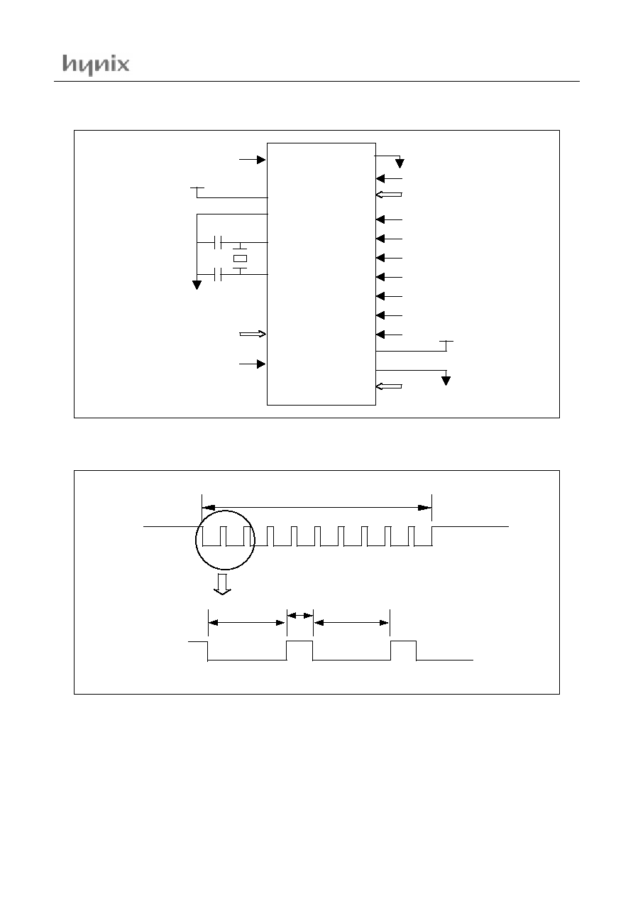
HMS91C7134
November.2001 ver1.0
75
Figure 21-1 Programming Configuration
Figure 21-2 PROG Waveform
RESET
VDD1
VSS1
XTAL2
XTAL1
P0
INT0/VPP
HSYNC
IN
VSYNC
IN
P2.0
-P2.5
P2.6
P2.7
P3.2/EA
P3.3/PSEN
P3.5/PROG
P3.6
P3.7
VDD2
VSS2
P1
PGM DATA
12.75 V
A7 - A0
A14
A13 - A8
0
1
1
0
PULSE
1
1
0
P3.5/PROG
10 PULSES
Enlarged View
100µs
10
100µs
10
Min 10µs
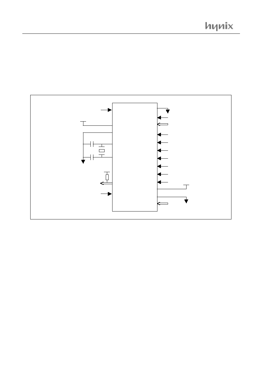
HMS91C7134
76
November.2001 ver1.0
·Program Verification
If Lock Bit 2 has not been programmed, the on-chip program
memory can be read out for program verification. The address of
the program memory location to be read is applied to port 1, 2 and
VSYNCIN as shown in Figure 21-4. The other pins are held at
the "Verify Code Data" levels indicated in Table 21.1. The con-
tents of the address location will be emitted on port 0 for this op-
eration. If the encryption table has been programmed, the data
presented at port 0 will be the exclusive NOR of the program byte
with one of the encryption bytes. The user will have to know the
encryption table contents in order to correctly decode the verifi-
cation data. The encryption table itself cannot be read out.
Figure 21-3 Verification Configuration
RESET
VDD1
VSS1
XTAL2
XTAL1
P0
INT0/VPP
PGM DATA
5 V
A7 - A0
A14
A13 - A8
0
0
1
0
1
1
1
HSYNC
IN
VSYNC
IN
P2.0
-P2.5
P2.6
P2.7
P3.2/EA
P3.3/PSEN
P3.5/PROG
P3.6
P3.7
VDD2
VSS2
P1
10k
0
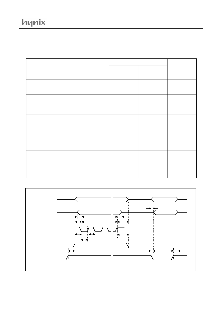
HMS91C7134
November.2001 ver1.0
77
EPROM Programming and Verification Characteristics
TA = 21
to 27
, Vcc = 5V + 10%, Vss = 0V
Figure 21-4 EPROM Programming and Verification
Programming supply voltage
Programming supply current
Oscillator frequency
Address setup to PROG low
Address hold after PROG
Data setup to PROG
Data hold after PROG
P2.7 (ENABLE) high to VPP
VPP setup to PROG
VPP hold after PROG
PROG width
Address to data valid
ENABLE low to data valid
Data float after ENABLE
PROG high to PROG low
VPP
IPP
1/
t
CLCL
t
AVGL
t
GHAX
t
DVGL
t
GHDX
t
EHSH
t
SHGL
t
GHSL
t
GLGL
t
AVQV
t
ELQV
t
EHQZ
t
GHGL
12.5
-
4
48
t
CLCL
48
t
CLCL
48
t
CLCL
48
t
CLCL
48
t
CLCL
10
10
90
-
-
0
10
13.0
50
6
-
-
-
-
-
-
-
110
48
t
CLCL
48
t
CLCL
48
t
CLCL
-
V
mA
MHz
-
-
-
-
-
µs
µs
µs
-
-
-
µs
Parameter
Symbol
Limit Values
Min
Max
Unit
P1.0 - P1.7
P2.0 - P2.5
VSYNC
IN
PORT0
P3.5/PROG
INT0/VPP
P2.7(ENABLE)
//
//
//
//
//
//
//
PROGRAMMING
VERIFICATION
ADDRESS
ADDRESS
DATA IN
DATA OUT
t
DVGL
t
AVGL
10 PULSES
t
GHDX
t
GHAX
t
AVQV
t
ELQV
t
EHQZ
t
EHSH
t
GHGL
t
GLGL
t
SHGL
t
GHSL
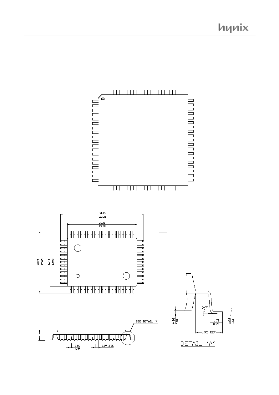
HMS91C7134
78
November.2001 ver1.0
21.2 64MQFP pinning and Package Dimensions
1
2
3
4
5
7
8
9
1 0
1 1
6
4 4
4 2
4 1
4 0
3 9
3 7
3 6
3 5
3 4
3 3
3 8
64
63
62
61
60
58
57
56
55
54
59
20
21
23
24
25
26
27
22
H M S 9 7 C 7 1 3 2
Y Y W W
1 2
1 3
1 4
1 5
1 6
29
30
31
32
28
4 8
4 7
4 6
4 5
53
52
4 3
N .C
N .C
V D D 1
V S S 1
X T A L 2
X T A L 1
B P 2 .7
B P 2 .6
S D A 2 * * /P 1 .7
S C L 2 * * /P 1 .6
B P 2 .5
B P 2 .4
P 0 .7
P 0 .6
P 0 .5
P 0 .4
IN
T
0
/V
P
P
P0
.
3
P0
.
2
P0
.
1
P0
.
0
BP2
.
3
BP2
.
2
ACH3
/
P
1
.
5
ACH2
/
P
1
.
4
ACH1
/
P
1
.
3
ACH0
/
P
1
.
2
SDA1
**/
P
1
.
1
SCL
1
**/
P
1
.
0
N .C
P W M 4 * /P 2 .6
P W M 5 * /P 2 .7
H S Y N C
O U T
/P 3 .2
V S Y N C
O U T
/P 3 .3
P W M 6 * /P 3 .4 /IN T 1
B P 2 .0
B P 2 .1
C L A M P /P W M 7 /P 3 .5 /P R O G
P A T O U T /P 3 .6
S O G
I N
/P 3 .7
R S T O U T
V D D 2
V S S 2
N .C
N .C
RE
S
E
T
P3
.
0
P3
.
1
D
P
W
M
0*
/
P
2.
0
D
P
W
M
1*
/
P
2.
1
PW
M
0
*
/
P2
.
2
EAN
AL
E
PSE
NN
VSY
NC
IN
HS
Y
N
C
IN
PW
M
1
*
/
P2
.
3
PW
M
2
*
/
P2
.
4
1 7
1 8
1 9
N .C
N .C
N .C
5 1
5 0
4 9
P W M 3 * /P 2 .5
N .C
N .C
3.18 MAX
NOTE
1. DIMENSIONS DO NOT INCLUDE MOLD PROTRUSION AND
DAMBAR PROTRUSION.
ALLOWABLE MOLD PROTRUSION IS 0.254mm.
ALLOWABLE DAMBAR PROTRUSION SHALL BE 0.08mm
TOTAL AT MAXIMUM MATERIAL CONDITION.
2. FORMED LEAD SHALL BE PLANAR WITH RESPECT ANOTHER
WITHIN 0.10mm
3. CONTROLLING DIMENSION : MILLIMETER.
THIS OUTLINE CONFIRMS TO JEDEC PUBLICATION 95
RESISTRATION MO-112.
HMS91C7134
November.2001 ver1.0
79
21.3 64MQFP Pin Description
PIN NAME
(Alternate)
Pin
No.
In/Out
(Alter-
nate)
Function
Basic
Alternate
N.C
1
-
No connection
N.C
2
-
No connection
V
DD1
3
-
Power supply1(+5V)
V
SS1
4
-
Ground1
XTAL2
5
O
Oscillator output pin for system clock
XTAL1
6
I
Oscillator input pin for system clock
BP2.7
7
I/O
External Access / Emulation port2.7
BP2.6
8
I/O
External Access / Emulation port2.6
SDA2 /P1.7
9
I/O
General I/O port P1.7
I
2
C serial data I/O port
SCL2 /P1.6
10
I/O
General I/O port P1.6
I
2
C serial clock I/O port
BP2.5
11
I/O
External Access / Emulation port2.5
BP2.4
12
I/O
External Access / Emulation port2.4
P0.7
13
I/O
General I/O port P0.7; adapted for LED driver
P0.6
14
I/O
General I/O port P0.6; adapted for LED driver
P0.5
15
I/O
General I/O port P0.5
P0.4
16
I/O
General I/O port P0.4
N.C
17
-
No connection
N.C
18
-
No connection
N.C
19
-
No connection
INT0 /V
PP
20
I
External interrupt input0; Programming supply voltage (during OTP programming)
P0.3
21
I/O
General I/O port P0.3
P0.2
22
I/O
General I/O port P0.2
P0.1
23
I/O
General I/O port P0.1
P0.0
24
I/O
General I/O port P0.0
BP2.3
25
I/O
External Access / Emulation port2.3
BP2.2
26
I/O
External Access / Emulation port2.2
ACH3 /P1.5
27
I/O
General I/O port P1.5
ADC channel3 input
ACH2 /P1.4
28
I/O
General I/O port P1.4
ADC channel2 input
ACH0 /P1.3
29
I/O
General I/O port P1.3
ADC channel1 input
ACH0 /P1.2
30
I/O
General I/O port P1.2
ADC channel0 input
SDA1 /P1.1
31
I/O
General I/O port P1.1
I
2
C serial data I/O port for DDC interface
SCL1 /P1.0
32
I/O
General I/O port P1.0
I
2
C serial clock I/O port for DDC interface
N.C
33
-
No connection
N.C
34
-
No connection
V
SS2
35
-
Ground2
V
DD2
36
-
Power supply2(+5V)
RSTOUT
37
O
RESET or Internal reset out / EH-IC reset signal; active High
SOGin /P3.7
38
I/O
General I/O port P3.7
Sync on Green input
Table 21-4 Port Function Description(64MQFP)
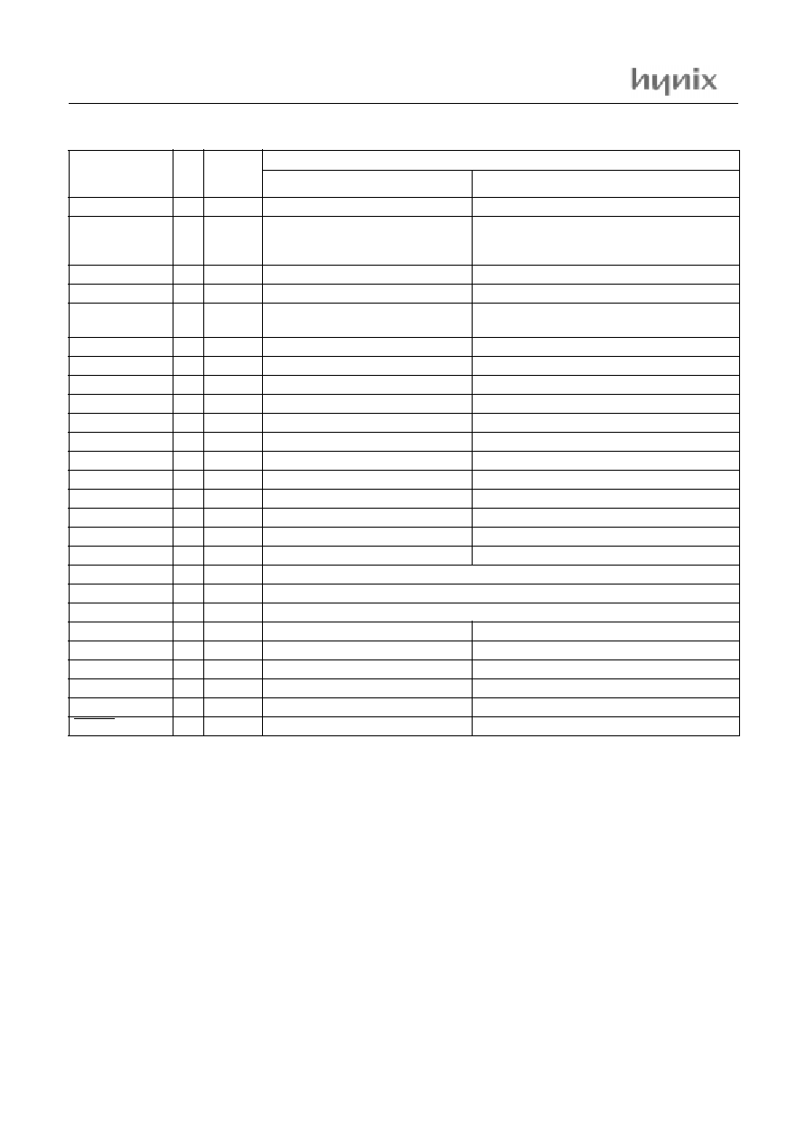
HMS91C7134
80
November.2001 ver1.0
PATOUT /P3.6
39
I/O
General I/O port P3.6
Pattern out
CLAMP /PWM7 /
P3.5 /PROG
40
I/O
General output only port P3.5
Program pulse input(during OTP
programming)
Clamp out ; 8-bit Pulse Width Modulation
output7
BP2.1
41
I/O
External Access / Emulation port2.1
BP2.0
42
I/O
External Access / Emulation port2.0
PWM6 /P3.4
INT1
43
I/O
General I/O port P3.4
8-bit Pulse Width Modulation output6; External
interrupt input1
VSYNCout /P3.3
44
I/O
General I/O port P3.3
Vertical sync output
HSYNCout /P3.2
45
I/O
General I/O port P3.2
Horizontal sync output
PWM5 /P2.7
46
I/O
General I/O port P2.7
8-bit Pulse Width Modulation output5
PWM4 /P2.6
47
I/O
General I/O port P2.6
8-bit Pulse Width Modulation output4
N.C
48
-
No connection
N.C
49
-
No connection
N.C
50
-
No connection
PWM3 /P2.5
51
I/O
General I/O port P2.5
8-bit Pulse Width Modulation output3
PWM2 /P2.4
52
I/O
General I/O port P2.4
8-bit Pulse Width Modulation output2
PWM1 /P2.3
53
I/O
General I/O port P2.3
8-bit Pulse Width Modulation output1
HSYNCin
54
I
Horizontal sync input
VSYNCin
55
I
Vertical sync input
PSENN
56
I/O
Program Store Enable Not / Emulation PSEN
ALE
57
I/O
Address Latch Enable / Emulation ALE
EAN
58
I/O
External Access Not / Emulation EA
PWM0 /P2.2
59
I/O
General I/O port P2.2
8-bit Pulse Width Modulation output0
DPWM0 /P2.1
60
I/O
General I/O port P2.1
8-bit Dynamic Pulse Width Modulation output0
DPWM0 /P2.0
61
I/O
General I/O port P2.0
8-bit Dynamic Pulse Width Modulation output1
P3.1
62
I/O
General I/O port P3.1
P3.0
63
I/O
General I/O port P3.0
RESET
64
I
Reset input
PIN NAME
(Alternate)
Pin
No.
In/Out
(Alter-
nate)
Function
Basic
Alternate
Table 21-4 Port Function Description(64MQFP)
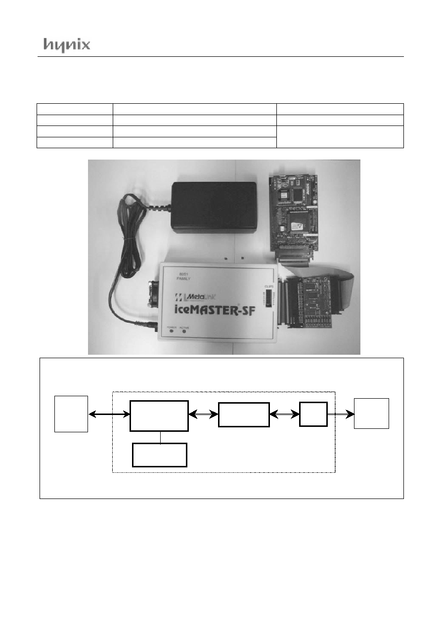
HMS91C7134
November.2001 ver1.0
81
21.4 Development Tools
The HMS9xC7134 is supported by a full-featured macro assembler / linker , an in-circuit emulator MetaICE
TM
.
Figure 21-5 Developement system Hardware Blockdiagram
Product
Developer
An agency in Korea
In Circuit Emulators
MetaICE
zeusemtek(www.emtek.co.kr)
Compiler
KEIL C51 Compiler, A51/A251 Assembler/Linker
Hankook MDS(www.hkmds.com)
Debugger
XHP3051.exe (Source-level Debugging)
PC
Monitor
Board
MetaLink
iceMASTER-SF
CONVERTER
POD
POWER
RS-232
Emulator
HMS91C7134
82
November.2001 ver1.0
22. INSTRUCTION SET
The HMS9xC7134 uses a powerful instruction set which permits
the expansion of on-chip CPU peripherals and optimizes byte ef-
ficiency and execution speed. Assigned opcodes add new high-
power operation and permit new addressing modes.
The instruction set consists of 49 single-byte, 46 two-byte and 16
three-byte instructions. When using a 12MHz oscillator, 64 in-
structions execute in 1us and 45 instructions execute in 2us. Mul-
tiply and divide instructions execute in 4 us.
For the description of the Date Addressing modes and Hexadeci-
mal opcode cross-reference see Boolean variable manipula-
tion,Program brranching.
·Arithmatic operations
Mnemonic
Description
Bytes
Cycles
Hex Code
ADD A, Rn
add register to A
1
1
2x
ADD A, direct
add direct byte to A
2
1
25
ADD A, @Ri
add indirect RAM to A
1
1
26,27
ADD A, #data
add immediate data to A
2
1
24
ADDC A, Rn
add register to A with carry flag
1
1
3x
ADDC A, direct add direct byte to A with carry flag
2
1
35
ADDC A, @Ri
add indirect RAM to A with carry flag
1
1
36,37
ADDC A, #data add immediate data to A with carry flag
2
1
34
SUBB A, Rn
subtract register from A with borrow
1
1
9x
SUBB A, direct
subtract direct byte from A with borrow
2
1
95
SUBB A, @Ri
subtract indirect RAM from A with borrow
1
1
96,97
SUBB A, #data
subtract immediate data from A with borrow
1
1
94
INC A
increment A
1
1
04
INC Rn
increment register
1
1
0x
INC direct
increment direct byte
INC
@Ri
increment indirect RAM
1
1
06,07
DEC A
decrement A
1
1
14
DEC Rn
decrement
Rn
1
1
1x
DEC direct
decrement direct byte
2
1
15
DEC @Ri
decrement indirect RAM
1
1
16,17
INC DTPR
increment data pointer
1
2
A3
MUL AB
multiply A and B
1
4
A4
DIV AB
divide A by B
1
4
84
DA A
decimal adjust A
1
1
D4
HMS91C7134
November.2001 ver1.0
83
·Logical operations
·Data transfer
Mnemonic
Description
Bytes
Cycles
Hex Code
ANL A, Rn
AND register to A
1
1
5x
ANL A, direct
AND direct byte to A
2
1
55
ANL A, @Ri
AND indirect RAM to A
1
1
56,57
ANL A, #data
AND immediate data to A
2
1
54
ANL direct, A
AND A to direct byte
2
1
52
ANL direct, #data
AND immediate data to direct byte
3
2
53
ORL A, Rn
OR register to A
1
1
4x
ORL A, direct
OR direct byte to A
2
1
45
ORL A, @Ri
OR indirect RAM to A
1
1
46,47
ORL A, #data
OR immediate data to A
2
1
44
ORL direct, A
OR A to direct byte
2
1
42
ORL direct, #data
OR immediate data to direct byte
3
2
43
XRL A, Rn
exclusive-OR register to A
1
1
6x
XRL A, direct
exclusive-OR direct byte to A
2
1
65
XRL A, @Ri
exclusive-OR indirect RAM to A
2
1
66,67
XRL A, #data
exclusive-OR immediate data to A
2
1
64
XRL direct, A
exclusive-OR A to direct byte
2
1
62
XRL direct, #data
exclusive-OR immediate data to direct byte
3
2
63
CLR A
clear A
1
1
E4
CPL A
complement A
1
1
F4
RL A
rotate A left
1
1
23
RLC A
rotate A left through the carry flag
1
1
33
RR A
rotate A right
1
1
03
RRC A
rotate A right through the carry flag
1
1
13
SWAP A
swap nibbles within A
1
1
C4
Mnemonic
Description
Bytes
Cycles
Hex Code
MOV A, Rn
move register to A
1
1
Ex
MOV A, direct
move direct byte to A
2
1
E5
MOV A, @Ri
move indirect RAM to A
1
1
E6,E7
MOV A, #data
move immediate data to A
2
1
74
MOV Rn, A
move A to register
1
1
Fx
MOV Rn, direct
move direct byte to register
2
2
Ax
MOV Rn, #data
move immediate data to register
2
1
7x
MOV direct, A
move A to direct byte
2
1
F5
MOV direct, Rn
move register to direct byte
2
2
8x
MOV direct, direct move direct byte to direct byte
3
2
85
HMS91C7134
84
November.2001 ver1.0
·Boolean variable manipulation
Note: * This command is not available under OTP Emulation Mode
Mnemonic
Description
Bytes
Cycles
Hex Code
MOV direct, @Ri
move indirect RAM to direct byte
2
2
86,87
MOV direct, #data move immediate data to direct byte
3
2
75
MOV @Ri, A
move A to indirect RAM
1
1
F6,F7
MOV @Ri, direct
move direct byte to indirect RAM
2
2
A6,A7
MOV @Ri, #data
move immediate data to indirect RAM
2
1
76,77
MOV DPTR, #data16 load data pointer with a 16-bit constant
3
2
90
MOVC A, @A+DPTR
move code byte relative to DPTR to A
1
2
93
MOVC A, @A+C
move code byte relative to PC to A
1
2
83
MOVX A, @Ri
move external RAM (8-bit address) to A
1
2
E2,E3
MOVX A, @DPTR
move external RAM (16-bit address) to A
1
2
E0
MOVX @Ri, A
move A to external RAM (8-bit address)
1
2
F2,F3
MOVX @DPTR, A
move A to external RAM (16-bit address)
1
2
F0
PUSH direct
push direct byte onto stack
2
2
C0
POP direct
pop direct byte from stack
2
2
D0
XCH A, Rn
exchange register with A
1
1
Cx
XCH A, direct
exchange direct byte with A
2
4
C5
XCH A, @Ri
exchange indirect RAM with A
1
1
C6,C7
XCHD A, @Ri
exchange LOW-order digit indirect RAM with A
1
1
D6,D7
Mnemonic
Description
Bytes
Cycles
Hex Code
CLR C
clear carry flag
1
1
C3
CLR bit
clear direct bit
2
1
C2
SETB C
set carry flag
1
1
D3
SETB bit
set direct bit
2
1
D2
CPL C
complement carry flag
1
1
B3
CPL bit
complement direct bit
2
1
B2
ANL C, bit
AND direct bit to carry flag
2
1
82
ANL C, /bit
AND complement of direct bit to carry flag
2
2
B0
OR C, bit
OR direct bit to carry flag
2
2
72
OR C, /bit
OR complement of direct bit to carry flag
2
2
A0
MOV C, bit
move direct bit to carry flag
2
1
A2
*MOV bit, C
move carry flag to direct bit
2
2
92
JC rel
jump if carry flag is set
2
2
40
JNC rel
jump if carry flag is not set
2
2
50
JB bit, rel
jump if direct bit is set
3
2
20
JNB bit, rel
jump if direct bit is not set
3
2
30
JBC bit, rel
jump if direct bit is set and clear bit
3
2
10
HMS91C7134
November.2001 ver1.0
85
·Program branching
·Data addressing modes
Mnemonic
Description
Bytes
Cycles
Hex Code
ACALL addr11
absolute subroutine call
2
2
y1
LCALL addr16
long subroutine call
3
1
12
RET
return from subroutine
1
2
22
RETI
return from interrupt
2
2
32
AJMP addr16
absolute jump
2
2
z1
LJMP addr16
long jump
3
2
02
SJMP addr16
short jump(relative address)
2
2
80
JMP @A+DPTR
jump indirect relative to the DPTR
1
2
73
JZ rel
jump if A is zero
2
2
60
JNZ rel
jump if A is not zero
2
2
70
CJNE A, direct, rel
compare direct byte to A and jump if not equal
3
2
B5
CJNE A, #data, rel
compare immediate data to A and jump if not equal
3
2
B4
CJNE Rn, #data, rel compare immediate data to register and jump if not
equal
3
2
Bx
CJNE A, @Ri, rel
compare immediate data to indirect RAM and jump if
not equal
3
2
B6,B7
DJNZ Rn, rel
decrement register and jump if not zero
2
2
Dx
DJNZ direct, rel
decrement direct byte and jump if not zero
3
2
D5
NOP
no operation
1
1
00
Mnemonic
Description
Rn
working register R0-R7
direct
128 internal RAM locations and any special function register (SFR)
@Ri
indirect internal RAM location addressed by register by register R0 or R1 of the actual register
bank
#data
8-bit constant included in instruction
#data16
16-bit constant included as bytes 2 and 3 of instruction
bit
direct addressed bit in internal RAM or SFR
addr16
16-bit destination address. Used by LCALL and LJMP;
the branch will be anywhere within the 64 kbytes Program Memory address space
addr11
111-bit destination address. Used by ACALL and AJMP;the branch will be within the
same 2 kbytes page of Program Memory as the first byte of the following instruction
rel
signed(two°Øs complement) 8-bit offset byte. Used by SJMP and all conditional jumps;
range is - 128 to + 127 bytes relative to first byte of the following instruction

HMS91C7134
86
November.2001 ver1.0
·Hexadecimal opcode cross-reference
Mnemonic
Description
x
8, 9, A, B, C, D, E, F
y
1, 3, 5, 7, 9, B, D, F
z
0, 2, 4, 6, 8, A, C, E
Document Outline
- HMS91C7134
- 1. OVERVIEW
- 2. BLOCK DIAGRAM
- 3. PIN ASSIGNMENT
- 4. PACKAGE DIMENSIONS
- 5. PIN FUNCTION
- 6. PORT STRUCTURES
- 7. ELECTRICAL CHARACTERISTICS
- 8. MEMORY ORGANIZATION
- 9. INTERRUPTS
- 10. POWER-SAVING MODE
- 11. I/O PORTS
- 12. OSCIALLTOR
- 13. RESET
- 14. WATCHDOG TIMER
- 15. TIMER
- 16. DDC INTERFACE
- Figure 16-1 DDC Interface block diagram
- 16.1 The Special Function register for DDC Interface.
- Eight SFR : S1CON, S1STA, S1DAT, S1ADR, RAMBUF, DDCCON, DDCADR, DDCDAT.
- S1CON, S1STA, S1DAT, S1ADR are just the copies of the corresponding registers in general I2C-bus ...
- Table 16-1 DDC mode status and DDC1 control register (DDCCON : 0D7H) RESET VALUE:x00x0000B
- This bit defines the size of the EDID data. It is related to the function of the post increment o...
- If EX_DAT is
- 1: The data size is 256 byte.
- 0: The data size is 128 byte(The addressing range for the EDID data buffer is mapped from 0 to 12...
- This bit indicates if the software/CPU is needed to take care of the operation of DDC1 protocol. ...
- 1 : In DDC1 protocol, CPU is interrupted during the period of the 9th transmitting bit so that th...
- 0 : The hold register of the transmitter will be automatically updated from the RAM buffer withou...
- Interrupt Request Bit. This bit is only valid in DDC1 protocol while S/W handling is enabled. Thi...
- 1 : Interrupt request is pending.
- 0 : No interrupt request
- DDC1 enable control bit. If DDC1EN is
- 1 : DDC1 is enabled.
- 0 : DDC1 is disabled ; The activity on VSYNC is ignored.
- Interrupt Request Bit. This bit is set by H/W when DDC interface switches from DDC1 to DDC2 (i.e....
- 1 : Interrupt request is pending.
- 0 : No interrupt request
- DDC mode indication bit. This bit will be set by H/W when the voltage transient from high to low ...
- 0: DDC1 is set.
- 1: DDC2 is set.
- 16.2 DDC1 protocol
- 16.3 DDC2B protocol
- 16.4 DDC2AB/DDC2B+ protocol
- 16.5 The RAM Buffer and DDC application
- 17. I2C INTERFACE
- 18. PULSE WIDTH MODULATION
- 19. SYNC PROCESSOR
- 20. ANALOG-TO-DIGITAL CONVERTOR (ADC)
- 21. OPERATION MODE
- 22. INSTRUCTION SET
- Arithmatic operations
- ADD A, Rn
- add register to A
- 1
- 1
- 2x
- ADD A, direct
- add direct byte to A
- 2
- 1
- 25
- ADD A, @Ri
- add indirect RAM to A
- 1
- 1
- 26,27
- ADD A, #data
- add immediate data to A
- 2
- 1
- 24
- ADDC A, Rn
- add register to A with carry flag
- 1
- 1
- 3x
- ADDC A, direct
- add direct byte to A with carry flag
- 2
- 1
- 35
- ADDC A, @Ri
- add indirect RAM to A with carry flag
- 1
- 1
- 36,37
- ADDC A, #data
- add immediate data to A with carry flag
- 2
- 1
- 34
- SUBB A, Rn
- subtract register from A with borrow
- 1
- 1
- 9x
- SUBB A, direct
- subtract direct byte from A with borrow
- 2
- 1
- 95
- SUBB A, @Ri
- subtract indirect RAM from A with borrow
- 1
- 1
- 96,97
- SUBB A, #data
- subtract immediate data from A with borrow
- 1
- 1
- 94
- INC A
- increment A
- 1
- 1
- 04
- INC Rn
- increment register
- 1
- 1
- 0x
- INC direct
- increment direct byte
- INC @Ri
- increment indirect RAM
- 1
- 1
- 06,07
- DEC A
- decrement A
- 1
- 1
- 14
- DEC Rn
- decrement Rn
- 1
- 1
- 1x
- DEC direct
- decrement direct byte
- 2
- 1
- 15
- DEC @Ri
- decrement indirect RAM
- 1
- 1
- 16,17
- INC DTPR
- increment data pointer
- 1
- 2
- A3
- MUL AB
- multiply A and B
- 1
- 4
- A4
- DIV AB
- divide A by B
- 1
- 4
- 84
- DA A
- decimal adjust A
- 1
- 1
- D4
- ANL A, Rn
- AND register to A
- 1
- 1
- 5x
- ANL A, direct
- AND direct byte to A
- 2
- 1
- 55
- ANL A, @Ri
- AND indirect RAM to A
- 1
- 1
- 56,57
- ANL A, #data
- AND immediate data to A
- 2
- 1
- 54
- ANL direct, A
- AND A to direct byte
- 2
- 1
- 52
- ANL direct, #data
- AND immediate data to direct byte
- 3
- 2
- 53
- ORL A, Rn
- OR register to A
- 1
- 1
- 4x
- ORL A, direct
- OR direct byte to A
- 2
- 1
- 45
- ORL A, @Ri
- OR indirect RAM to A
- 1
- 1
- 46,47
- ORL A, #data
- OR immediate data to A
- 2
- 1
- 44
- ORL direct, A
- OR A to direct byte
- 2
- 1
- 42
- ORL direct, #data
- OR immediate data to direct byte
- 3
- 2
- 43
- XRL A, Rn
- exclusive-OR register to A
- 1
- 1
- 6x
- XRL A, direct
- exclusive-OR direct byte to A
- 2
- 1
- 65
- XRL A, @Ri
- exclusive-OR indirect RAM to A
- 2
- 1
- 66,67
- XRL A, #data
- exclusive-OR immediate data to A
- 2
- 1
- 64
- XRL direct, A
- exclusive-OR A to direct byte
- 2
- 1
- 62
- XRL direct, #data
- exclusive-OR immediate data to direct byte
- 3
- 2
- 63
- CLR A
- clear A
- 1
- 1
- E4
- CPL A
- complement A
- 1
- 1
- F4
- RL A
- rotate A left
- 1
- 1
- 23
- RLC A
- rotate A left through the carry flag
- 1
- 1
- 33
- RR A
- rotate A right
- 1
- 1
- 03
- RRC A
- rotate A right through the carry flag
- 1
- 1
- 13
- SWAP A
- swap nibbles within A
- 1
- 1
- C4
- MOV A, Rn
- move register to A
- 1
- 1
- Ex
- MOV A, direct
- move direct byte to A
- 2
- 1
- E5
- MOV A, @Ri
- move indirect RAM to A
- 1
- 1
- E6,E7
- MOV A, #data
- move immediate data to A
- 2
- 1
- 74
- MOV Rn, A
- move A to register
- 1
- 1
- Fx
- MOV Rn, direct
- move direct byte to register
- 2
- 2
- Ax
- MOV Rn, #data
- move immediate data to register
- 2
- 1
- 7x
- MOV direct, A
- move A to direct byte
- 2
- 1
- F5
- MOV direct, Rn
- move register to direct byte
- 2
- 2
- 8x
- MOV direct, direct
- move direct byte to direct byte
- 3
- 2
- 85
- MOV direct, @Ri
- move indirect RAM to direct byte
- 2
- 2
- 86,87
- MOV direct, #data
- move immediate data to direct byte
- 3
- 2
- 75
- MOV @Ri, A
- move A to indirect RAM
- 1
- 1
- F6,F7
- MOV @Ri, direct
- move direct byte to indirect RAM
- 2
- 2
- A6,A7
- MOV @Ri, #data
- move immediate data to indirect RAM
- 2
- 1
- 76,77
- MOV DPTR, #data16
- load data pointer with a 16-bit constant
- 3
- 2
- 90
- MOVC A, @A+DPTR
- move code byte relative to DPTR to A
- 1
- 2
- 93
- MOVC A, @A+C
- move code byte relative to PC to A
- 1
- 2
- 83
- MOVX A, @Ri
- move external RAM (8-bit address) to A
- 1
- 2
- E2,E3
- MOVX A, @DPTR
- move external RAM (16-bit address) to A
- 1
- 2
- E0
- MOVX @Ri, A
- move A to external RAM (8-bit address)
- 1
- 2
- F2,F3
- MOVX @DPTR, A
- move A to external RAM (16-bit address)
- 1
- 2
- F0
- PUSH direct
- push direct byte onto stack
- 2
- 2
- C0
- POP direct
- pop direct byte from stack
- 2
- 2
- D0
- XCH A, Rn
- exchange register with A
- 1
- 1
- Cx
- XCH A, direct
- exchange direct byte with A
- 2
- 4
- C5
- XCH A, @Ri
- exchange indirect RAM with A
- 1
- 1
- C6,C7
- XCHD A, @Ri
- exchange LOW-order digit indirect RAM with A
- 1
- 1
- D6,D7
- CLR C
- clear carry flag
- 1
- 1
- C3
- CLR bit
- clear direct bit
- 2
- 1
- C2
- SETB C
- set carry flag
- 1
- 1
- D3
- SETB bit
- set direct bit
- 2
- 1
- D2
- CPL C
- complement carry flag
- 1
- 1
- B3
- CPL bit
- complement direct bit
- 2
- 1
- B2
- ANL C, bit
- AND direct bit to carry flag
- 2
- 1
- 82
- ANL C, /bit
- AND complement of direct bit to carry flag
- 2
- 2
- B0
- OR C, bit
- OR direct bit to carry flag
- 2
- 2
- 72
- OR C, /bit
- OR complement of direct bit to carry flag
- 2
- 2
- A0
- MOV C, bit
- move direct bit to carry flag
- 2
- 1
- A2
- *MOV bit, C
- move carry flag to direct bit
- 2
- 2
- 92
- JC rel
- jump if carry flag is set
- 2
- 2
- 40
- JNC rel
- jump if carry flag is not set
- 2
- 2
- 50
- JB bit, rel
- jump if direct bit is set
- 3
- 2
- 20
- JNB bit, rel
- jump if direct bit is not set
- 3
- 2
- 30
- JBC bit, rel
- jump if direct bit is set and clear bit
- 3
- 2
- 10
- ACALL addr11
- absolute subroutine call
- 2
- 2
- y1
- LCALL addr16
- long subroutine call
- 3
- 1
- 12
- RET
- return from subroutine
- 1
- 2
- 22
- RETI
- return from interrupt
- 2
- 2
- 32
- AJMP addr16
- absolute jump
- 2
- 2
- z1
- LJMP addr16
- long jump
- 3
- 2
- 02
- SJMP addr16
- short jump(relative address)
- 2
- 2
- 80
- JMP @A+DPTR
- jump indirect relative to the DPTR
- 1
- 2
- 73
- JZ rel
- jump if A is zero
- 2
- 2
- 60
- JNZ rel
- jump if A is not zero
- 2
- 2
- 70
- CJNE A, direct, rel
- compare direct byte to A and jump if not equal
- 3
- 2
- B5
- CJNE A, #data, rel
- compare immediate data to A and jump if not equal
- 3
- 2
- B4
- CJNE Rn, #data, rel
- compare immediate data to register and jump if not equal
- 3
- 2
- Bx
- CJNE A, @Ri, rel
- compare immediate data to indirect RAM and jump if not equal
- 3
- 2
- B6,B7
- DJNZ Rn, rel
- decrement register and jump if not zero
- 2
- 2
- Dx
- DJNZ direct, rel
- decrement direct byte and jump if not zero
- 3
- 2
- D5
- NOP
- no operation
- 1
- 1
- 00
- Rn
- working register R0-R7
- direct
- 128 internal RAM locations and any special function register (SFR)
- @Ri
- indirect internal RAM location addressed by register by register R0 or R1 of the actual register ...
- #data
- 8-bit constant included in instruction
- #data16
- 16-bit constant included as bytes 2 and 3 of instruction
- bit
- direct addressed bit in internal RAM or SFR
- addr16
- 16-bit destination address. Used by LCALL and LJMP;
- the branch will be anywhere within the 64 kbytes Program Memory address space
- addr11
- 111-bit destination address. Used by ACALL and AJMP;the branch will be within the
- same 2 kbytes page of Program Memory as the first byte of the following instruction
- rel
- signed(two°Øs complement) 8-bit offset byte. Used by SJMP and all conditional jumps;
- range is - 128 to + 127 bytes relative to first byte of the following instruction
- x
- 8, 9, A, B, C, D, E, F
- y
- 1, 3, 5, 7, 9, B, D, F
- z
- 0, 2, 4, 6, 8, A, C, E