 | ÐлекÑÑоннÑй компоненÑ: HMS99C52 | СкаÑаÑÑ:  PDF PDF  ZIP ZIP |
Äîêóìåíòàöèÿ è îïèñàíèÿ www.docs.chipfind.ru

HYNIX SEMICONDUCTOR INC.
8-BIT SINGLE-CHIP MICROCONTROLLERS
HMS99C51
HMS99C52
User's Manual (Ver. 1.0)

Version 1.0
Published by
MCU Application Team
2002
Hynix semiconductor All right reserved.
Additional information of this manual may be served by Hynix semiconductor offices in Korea or Distributors
and Representatives listed at address directory.
Hynix semiconductor reserves the right to make changes to any information here in at any time without notice.
The information, diagrams and other data in this manual are correct and reliable; however, Hynix semiconduc-
tor is in no way responsible for any violations of patents or other rights of the third party generated by the use
of this manual.
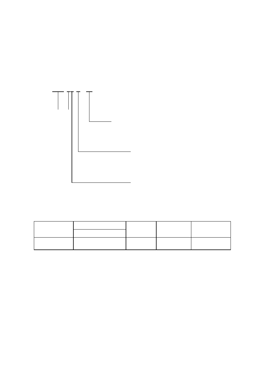
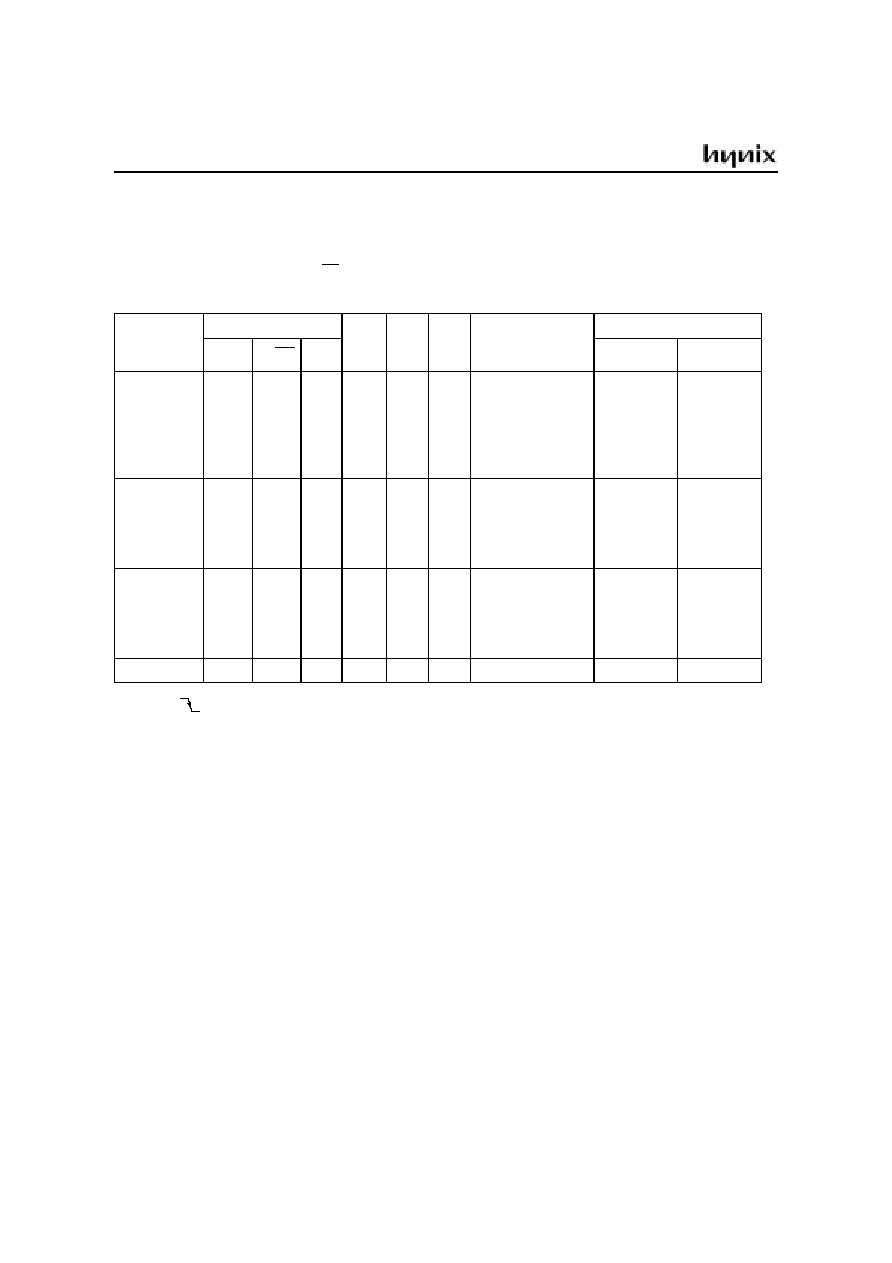
Device Naming Structure
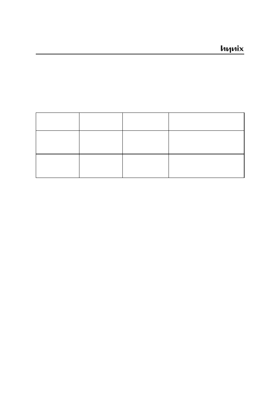
HMS99C5X Series Selection Guide
Operating
Voltage (V)
ROM size (bytes)
RAM size
(bytes)
Device Name
Operating
Frequency (MHz)
FLASH
4.5~5.5
4K
8K
128
256
HMS99C51
HMS99C52
40
40
XX
HMS99X5X
Package Type
Blank:
PL:
Q:
40PDIP
44PLCC
44MQFP
ROM size
1:
2:
4k bytes
8k bytes
Operating Voltage
C: 4.5~5.5V
Hyn
i
x
se
mi
co
ndu
cto
r
M
C
U
FLASH v
e
rs
io
n
HMS99C5X Series
0
Jan. 2003 Ver 1.0
HMS99C51
· Fully compatible to standard MCS-51 microcontroller
· Wide operating frequency up to 40MHz
(for more detail, see "HMS99C5X Series Selection Guide")
· X2 Speed Improvement capability ( X2 Mode : 6 clocks/machine cycle)
20MHz @5V (Equivalent to 40MHz @5V)
· 4K bytes FLASH ROM
· 128
×
8Bit RAM
· 64K external program memory space
· 64K external data memory space
· Four 8-bit ports
· Two 16-bit Timers / Counters
· USART
· Programmable ALE pin enable / disable (Low EMI)
· Five interrupt sources, two priority levels
· Power saving Idle and power down mode
· P-DIP-40, P-LCC-44, P-MQFP-44 package
· Temperature Ranges :
-40
°
C ~ 85
°
C
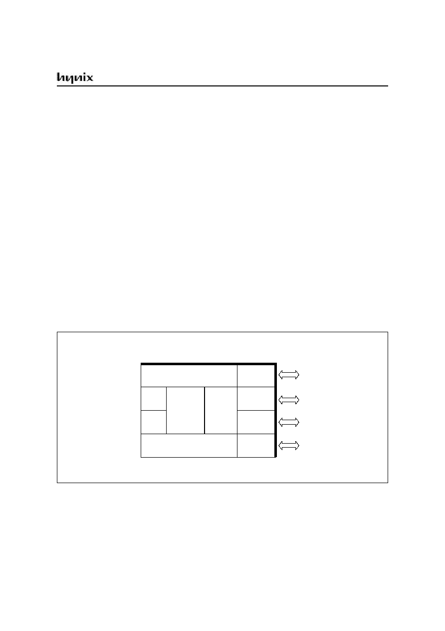
Block Diagram
RAM
128
×
8
PORT 0
PORT 1
PORT 3
PORT 2
8-BIT
USART
FLASH ROM
4K
×
8
CPU
T 0
T 1
I/O
I/O
I/O
I/O
HMS99C5X Series
Jan. 2003 Ver 1.0
1
HMS99C52
· Fully compatible to standard MCS-51 microcontroller
· Wide operating frequency up to 40MHz
(for more detail, see "HMS99C5X Series Selection Guide")
· X2 Speed Improvement capability ( X2 Mode : 6 clocks/machine cycle)
20MHz @5V (Equivalent to 40MHz @5V)
· 8K bytes FLASH ROM
· 256
×
8Bit RAM
· 64K external program memory space
· 64K external data memory space
· Four 8-bit ports
· Three 16-bit Timers / Counters (Timer2 with up/down counter feature)
· USART
· One clock output port
· Programmable ALE pin enable / disable (Low EMI)
· Six interrupt sources, two priority levels
· Power saving Idle and power down mode
· P-DIP-40, P-LCC-44, P-MQFP-44 package
· Temperature Ranges :
-40
°
C ~ 85
°
C
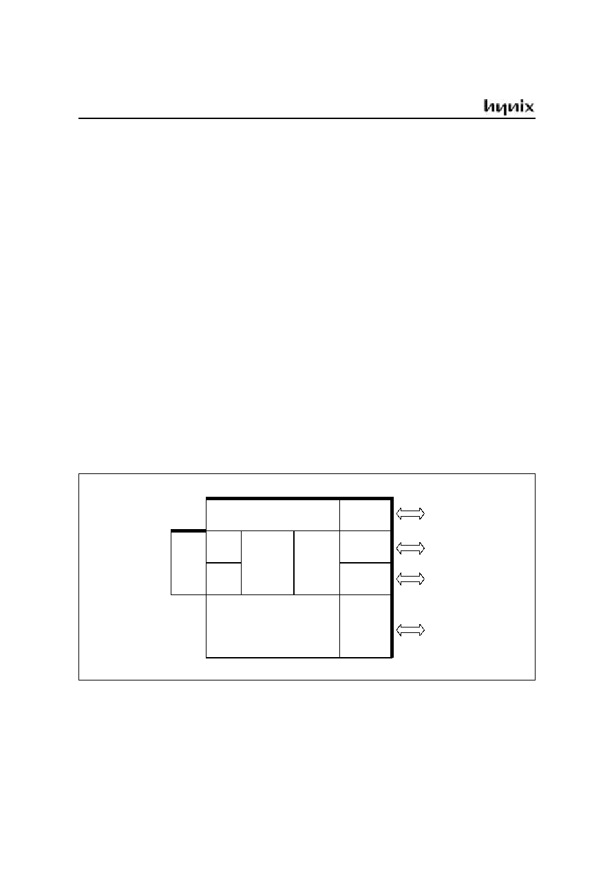
Block Diagram
RAM
256
×
8
PORT 0
PORT 1
PORT 3
PORT 2
8-BIT
USART
FLASH ROM
8K
×
8
CPU
T 0
T 1
I/O
I/O
I/O
I/O
T 2
HMS99C5X Series
2
Jan. 2003 Ver 1.0
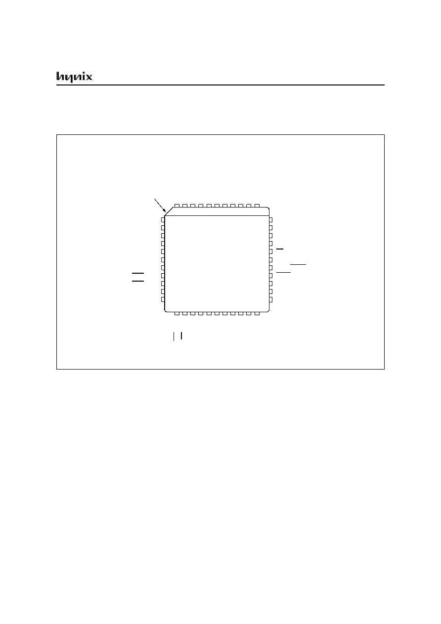
PIN CONFIGURATION
44-PLCC Pin Configuration (top view)
P0.4 / AD4
P0.5 / AD5
P0.6 / AD6
P0.7 / AD7
EA / V
PP
N.C.*
ALE / PROG
PSEN
P2.7 / A15
P2.6 / A14
P2.5 / A13
P1.5
P1.6
P1.7
RESET
RxD / P3.0
N.C.*
TxD / P3.1
INT0 / P3.2
INT1 / P3.3
T0 / P3.4
T1 / P3.5
WR
/
P
3
.6
RD
/
P
3
.7
XTAL
2
XTAL
1
V
SS
N.
C.*
P
2
.0
/ A
8
P
2
.1
/ A
9
P2
.
2
/
A1
0
P
2
.
3
/
A
1
1
P2
.
4
/
A1
2
P1
.
4
P1
.
3
P1
.
2
P1
.
1
/
T
2
EX
P
1
.
0
/
T
2
N.C.
*
V
CC
P
0
.
0
/
A
D
0
P
0
.
1
/
A
D
1
P
0
.
2
/
A
D
2
P
0
.
3
/
A
D
3
6
5
4
3
2
1
44
43
42
41
40
18
19
20
21
22
23
24
25
26
27
28
39
38
37
36
35
34
33
32
31
30
29
7
8
9
10
11
12
13
14
15
16
17
INDEX
CORNER
N.C.: Do not connect.
HMS99C5X Series
Jan. 2003 Ver 1.0
3
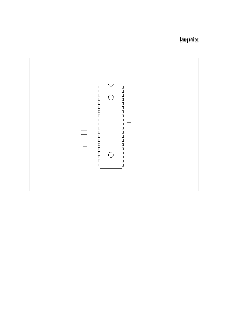
40-PDIP Pin Configuration (top view)
P0.4 / AD4
P0.5 / AD5
P0.6 / AD6
P0.7 / AD7
EA / V
PP
ALE / PROG
PSEN
P2.7 / A15
P2.6 / A14
P2.5 / A13
39
38
37
36
35
34
33
32
31
30
29
28
27
26
25
24
23
22
21
40
P2.4 / A12
P2.3 / A11
P2.2 / A10
P2.1 / A9
P2.0 / A8
P0.0 / AD0
P0.1 / AD1
P0.2 / AD2
P0.3 / AD3
V
CC
T2EX / P1.1
P1.2
P1.3
P1.4
T2 / P1.0
P1.5
P1.6
P1.7
RESET
RxD / P3.0
TxD / P3.1
INT0 / P3.2
INT1 / P3.3
T0 / P3.4
T1 / P3.5
WR / P3.6
RD / P3.7
XTAL2
XTAL1
V
SS
2
3
4
5
6
7
8
9
10
11
12
13
14
15
16
17
18
19
20
1
HMS99C5X Series
4
Jan. 2003 Ver 1.0
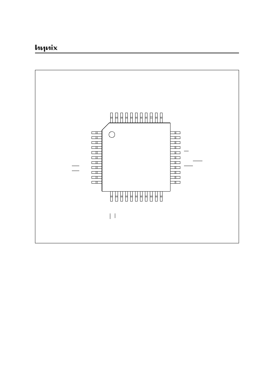
44-MQFP Pin Configuration (top view)
P0.4 / AD4
P0.5 / AD5
P0.6 / AD6
P0.7 / AD7
EA / V
PP
N.C.*
ALE / PROG
PSEN
P2.7 / A15
P2.6 / A14
P2.5 / A13
P1.5
P1.6
P1.7
RESET
RxD / P3.0
N.C.*
TxD / P3.1
INT0 / P3.2
INT1 / P3.3
T0 / P3.4
T1 / P3.5
WR
/
P
3
.6
RD
/
P
3
.7
XTAL
2
XTAL
1
V
SS
N.C
.
*
P
2
.0
/ A
8
P
2
.1
/ A
9
P2
.
2
/
A1
0
P
2
.
3
/
A
1
1
P2
.
4
/
A1
2
P1
.
4
P1
.
3
P1
.
2
P1
.
1
/
T
2
EX
P
1
.0 /
T
2
N.
C.*
V
CC
P0
.
0
/
AD0
P0
.
1
/
AD1
P0
.
2
/
AD2
P0
.
3
/
AD3
44
43
42
41
40
39
38
37
36
35
34
12
13
14
15
16
17
18
19
20
21
22
33
32
31
30
29
28
27
26
25
24
23
1
2
3
4
5
6
7
8
9
10
11
N.C.: Do not connect.
HMS99C5X Series
Jan. 2003 Ver 1.0
5
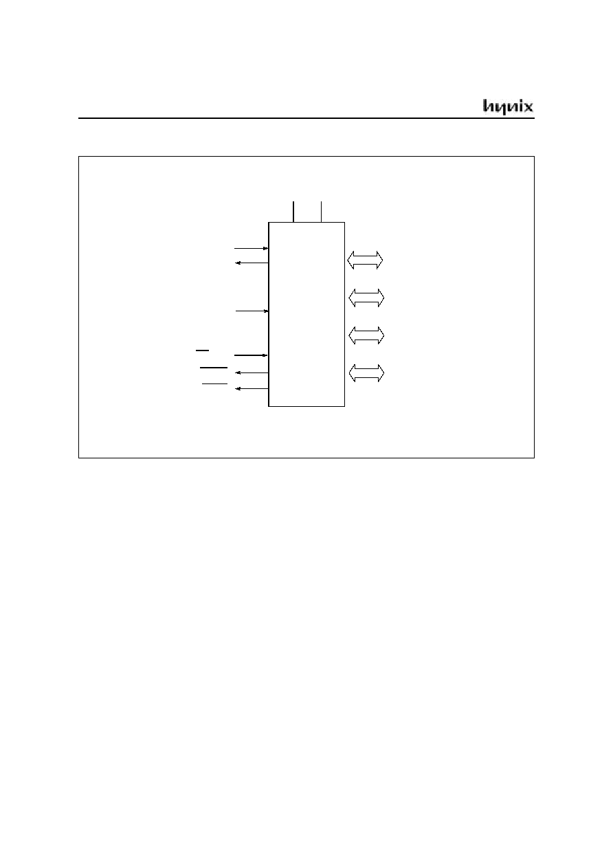
Logic Symbol
XTAL1
XTAL2
RESET
Port 0
8-bit Digital I/O
Port 1
8-bit Digital I/O
Port 2
8-bit Digital I/O
Port 3
8-bit Digital I/O
EA/V
PP
ALE/PROG
PSEN
V
CC
V
SS
HMS99C5X Series
6
Jan. 2003 Ver 1.0
PIN DEFINITIONS AND FUNCTIONS
Symbol
Pin Number
Input/
Output
Function
PLCC-
44
PDIP-
40
MQFP-
44
P1.0-P1.7
2-9
2
3
2
1-8
1
2
1
40-44,
1-3
40
41
40
I/O
Port1
Port 1 is an 8-bit bidirectional I/O port with internal
pull-ups. Port 1 pins that have 1s written to them are
pulled high by the internal pull-up resistors and can be
used as inputs. As inputs, port 1 pins that are
externally pulled low will source current because of
the pulls-ups (I
IL
, in the DC characteristics). Pins P1.0
and P1.1 also. Port1 also receives the low-order
address byte during program memory verification.
Port1 also serves alternate functions of Timer 2.
P1.0 / T2 :Timer/counter 2 external count input
P1.1 / T2EX :Timer/counter 2 trigger input
In HMS99C52:
P1.0 / T2, Clock Out : Timer/counter 2 external count
input, Clock Out
P3.0-P3.7
11,
13-19
10-17
5, 7-13
I/O
Port 3
Port 3 is an 8-bit bidirectional I/O port with internal
pull-ups. Port 3 pins that have 1s written to them are
pulled high by the internal pull-up resistors and can be
used as inputs. As inputs, port 3 pins that are
externally pulled low will source current because of
the pulls-ups (I
IL
, in the DC characteristics). Port 3 also
serves the special features of the 80C51 family, as
listed below.
11
13
14
15
16
17
18
19
10
11
12
13
14
15
16
17
5
7
8
9
10
11
12
13
P3.0 / RxD
P3.1 / TxD
P3.2 /INT0
P3.3 / INT1
P3.4 /T0
P3.5 /T1
P3.6 / WR
P3.7 /RD
receiver data input (asynchronous) or
data input output(synchronous) of serial
interface 0
transmitter data output (asynchronous)
or clock output (synchronous) of the
serial interface 0
interrupt 0 input/timer 0 gate control
interrupt 1 input/timer 1 gate control
counter 0 input
counter 1 input
the write control signal latches the data
byte from port 0 into the external data
memory
the read control signal enables the
external data memory to port 0
XTAL2
20
18
14
O
XTAL2
Output of the inverting oscillator amplifier.
HMS99C5X Series
Jan. 2003 Ver 1.0
7
XTAL1
21
19
15
I
XTAL1
Input to the inverting oscillator amplifier and input to
the internal clock generator circuits.To drive the
device from an external clock source, XTAL1 should
be driven, while XTAL2 is left unconnected. There are
no requirements on the duty cycle of the external
clock signal, since the input to the internal clocking
circuitry is divided down by a divide-by-two flip-flop.
Minimum and maximum high and low times as well as
rise fall times specified in the AC characteristics must
be observed.
P2.0-P2.7
24-31
21-28
18-25
I/O
Port 2
Port 2 is an 8-bit bidirectional I/O port with internal
pull-ups. Port 2 pins that have 1s written to them are
pulled high by the internal pull-up resistors and can be
used as inputs. As inputs, port 2 pins that are
externally pulled low will source current because of
the pulls-ups (I
IL
, in the DC characteristics).Port 2
emits the high-order address byte during fetches from
external program memory and during accesses to
external data memory that use 16-bit addresses
(MOVX @DPTR). In this application it uses strong
internal pull-ups when emitting 1s. During accesses to
external data memory that use 8-bit addresses
(MOVX @Ri), port 2 emits the contents of the P2
special function register.
PSEN
32
29
26
O
The Program Store Enable
The read strobe to external program memory when
the device is executing code from the external
program memory. PSEN is activated twice each
machine cycle, except that two PSEN activations are
skipped during each access to external data memory.
PSEN is not activated during fetches from internal
program memory.
RESET
10
9
4
I
RESET
A high level on this pin for two machine cycles while
the oscillator is running resets the device. An internal
diffused resistor to V
SS
permits power-on reset using
only an external capacitor to V
CC
.
Symbol
Pin Number
Input/
Output
Function
PLCC-
44
PDIP-
40
MQFP-
44
HMS99C5X Series
8
Jan. 2003 Ver 1.0
ALE /
PROG
33
30
27
O
The Address Latch Enable / Program pulse
Output pulse for latching the low byte of the address
during an access to external memory. In normal
operation, ALE is emitted at a constant rate of 1/6 the
oscillator frequency, and can be used for external
timing or clocking. Note that one ALE pulse is skipped
during each access to external data memory. This pin
is also the program pulse input (PROG) during
EPROM programming.
If desired, ALE operation can be disabled by setting
bit 0 of SFR location 8E
H
. With this bit set, the pin is
weakly pulled high. The ALE disable feature will be
terminated by reset. Setting the ALE-disable bit has
no affect if the microcontroller is in external execution
mode.
EA / V
PP
35
31
29
I
External Access Enable / Program Supply Voltage
EA must be external held low to enable the device to
fetch code from external program memory locations
0000
H
to FFFF
H
. If EA is held high, the device
executes from internal program memory unless the
program counter contains an address greater than its
internal memory size. This pin also receives the
12.75V programming supply voltage (V
PP
) during
EPROM programming.
Note;
however, that if any of the Lock bits are
programmed, EA will be internally
latched on reset.
P0.0-P0.7
36-43
32-39
30-37
I/O
Port 0
Port 0 is an 8-bit open-drain bidirectional I/O port.
Port 0 pins that have 1s written to them float and can
be used as high-impedance inputs.
Port 0 is also the multiplexed low-order address and
data bus during accesses to external program and
data memory. In this application it uses strong internal
pull-ups when emitting 1s. Port 0 also outputs the
code bytes during program verification in the
GMS97X5X. External pull-up resistors are required
during program verification.
V
SS
22
20
16
-
Circuit ground potential
V
CC
44
40
38
-
Supply terminal for all operating modes
N.C.
1,12
23,34
-
6,17
28,39
-
No connection
Symbol
Pin Number
Input/
Output
Function
PLCC-
44
PDIP-
40
MQFP-
44
HMS99C5X Series
Jan. 2003 Ver 1.0
9
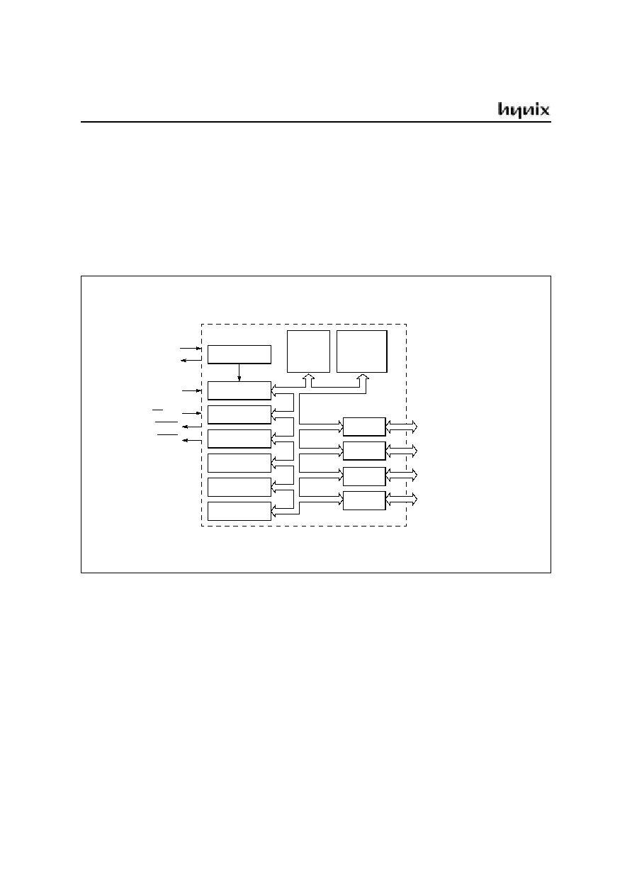
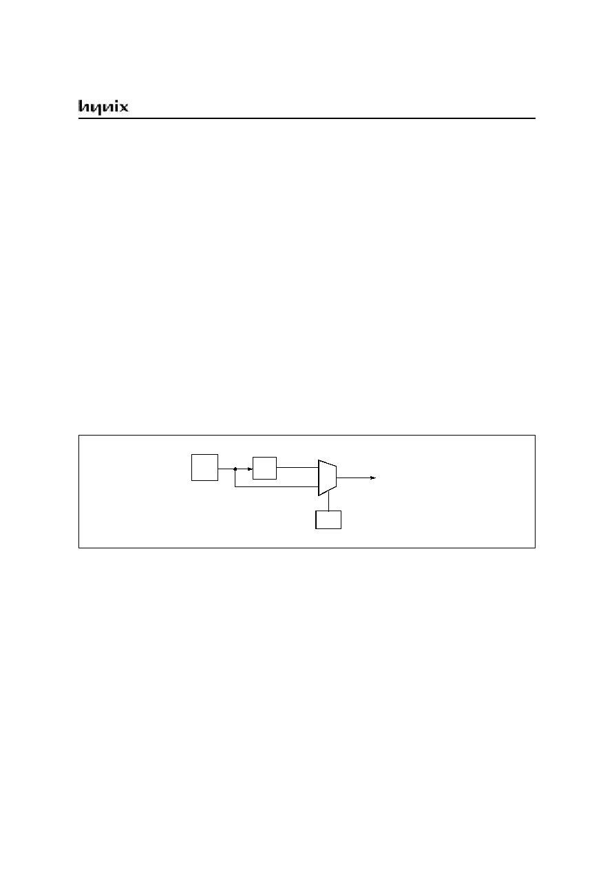
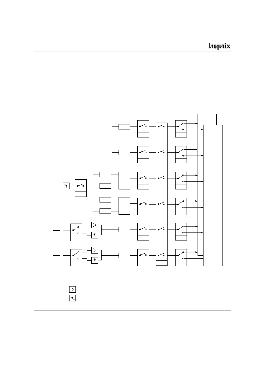
FUNCTIONAL DESCRIPTION
The HMS99C5X series is fully compatible to the standard 8051 microcontroller family.
It is compatible with the general 8051 family. While maintaining all architectural and operational characteristics
of the general 8051 family.
Figure 1 shows a block diagram of the HMS99C5X series
Figure 1. Block Diagram of the HMS99C5X series
FRASH
4K/8K
RAM
128/256
×
8
OSC & TIMING
CPU
Timer 0
Timer 1
Timer 2
Interrupt Unit
Serial Channel
Port 0
Port 1
Port 2
Port 3
Port 0
8-bit Digit. I/O
Port 1
8-bit Digit. I/O
Port 2
8-bit Digit. I/O
Port 3
8-bit Digit. I/O
XTAL1
XTAL2
RESET
EA/V
PP
ALE/PROG
PSEN
HMS99C5X Series
10
Jan. 2003 Ver 1.0
CPU
The HMS99C5X series is efficient both as a controller and as an arithmetic processor. It has extensive facilities
for binary and BCD arithmetic and excels in its bit-handling capabilities. Efficient use of program memory re-
sults from an instruction set consisting of 44% one-byte, 41% two-byte, and 15% three-byte instructions. With
a 12 MHz crystal, 58% of the instructions are executed in 1.0
µ
s (40MHz: 300ns).
Special Function Register PSW
Reset value of PSW is 00
H
.
Bit
Function
CY
Carry Flag
AC
Auxiliary Carry Flag (for BCD operations)
F0
General Purpose Flag
RS1
0
0
1
1
RS0
0
1
0
1
Register Bank select control bits
Bank 0 selected, data address 00
H
- 07
H
Bank 1 selected, data address 08
H
- 0F
H
Bank 2 selected, data address 10
H
- 17
H
Bank 3 selected, data address 18
H
- 1F
H
OV
Overflow Flag
F1
General Purpose Flag
P
Parity Flag
Set/cleared by hardware each instruction cycle to indicate an odd/even
number of "one" bits in the accumulator, i.e. even parity.
CY
AC
F0
RS1 RS0 OV
F1
P
7
6
5
4
3
2
1
0
LSB
MSB
Bit No.
Addr. D0
H
PSW
HMS99C5X Series
Jan. 2003 Ver 1.0
11
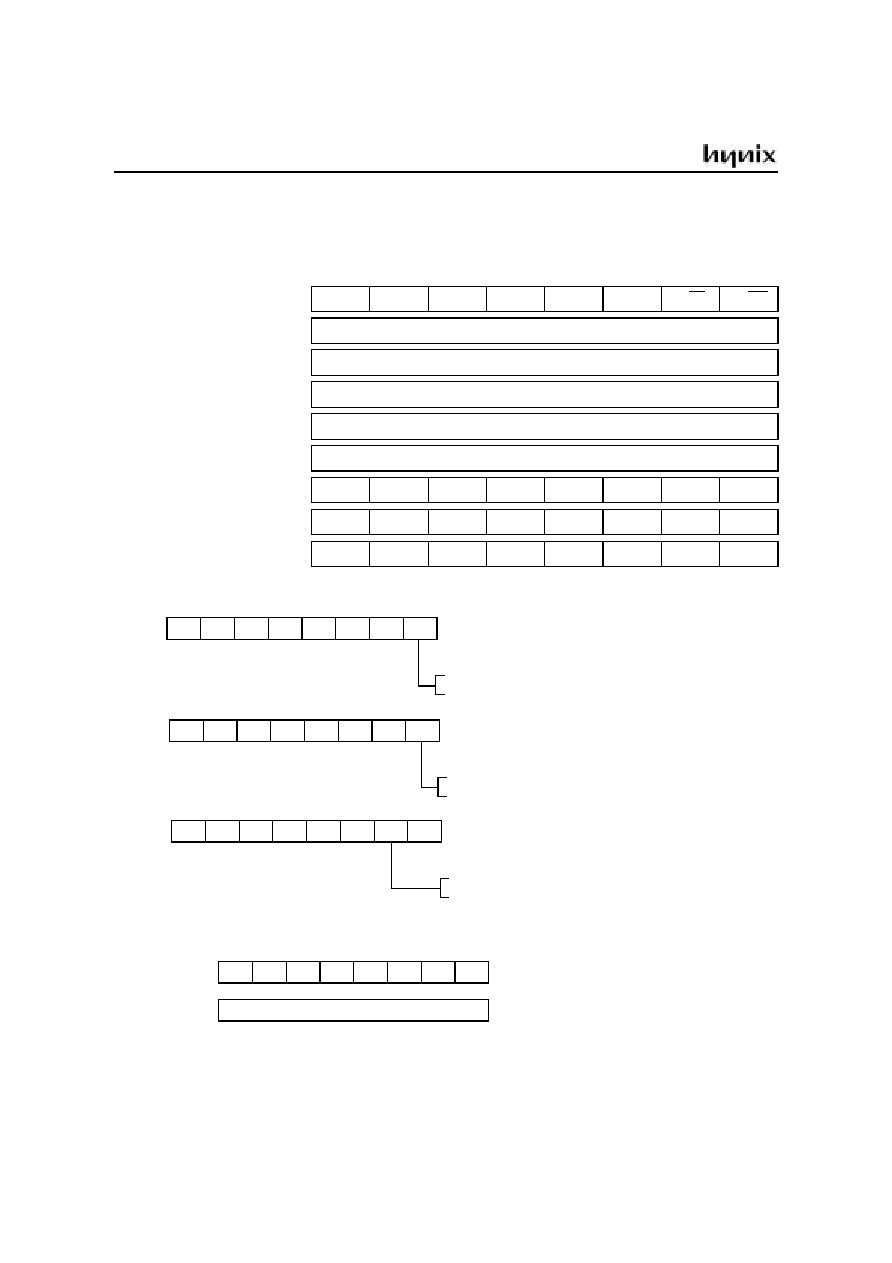
SPECIAL FUNCTION REGISTERS
All registers, except the program counter and the four general purpose register banks, reside in the special func-
tion register area.
The 28 special function registers (SFR) include pointers and registers that provide an interface between the CPU
and the other on-chip peripherals. There are also 128 directly addressable bits within the SFR area.
All SFRs are listed in Table 1, Table 2, and Table 3.
In Table 1 they are organized in numeric order of their addresses. In Table 2 they are organized in groups which
refer to the functional blocks of the HMS99C5X series. Table 3 illustrates the contents of the SFRs
Table 1. Special Function Registers in Numeric Order of their Addresses (cont'd)
Address
Register
Contents after
Reset
Address
Register
Contents after
Reset
80H
81H
82H
83H
84H
85H
86H
87H
P0
1)
SP
DPL
DPH
reserved
reserved
reserved
PCON
FFH
07H
00H
00H
XXH
2)
XXH
2)
XXH
2)
0XXX0000
B
2)
88H
89H
8AH
8BH
8CH
8DH
8EH
8FH
TCON
1)
TMOD
TL0
TL1
TH0
TH1
AUXR0
CKCON
00H
00H
00H
00H
00H
00H
XXH
2)
XXXXXXX0
B
2)
90H
91H
92H
93H
94H
95H
96H
97H
P1
1)
reserved
reserved
reserved
reserved
reserved
reserved
reserved
FF
H
00
H
XXH
2)
XXH
2)
XXH
2)
XXH
2)
XXH
2)
XXH
2)
98H
99H
9AH
9BH
9CH
9DH
9EH
9FH
SCON
1)
SBUF
reserved
reserved
reserved
reserved
reserved
reserved
00H
XXH
2)
XXH
2)
XXH
2)
XXH
2)
XXH
2)
XXH
2)
XXH
2)
A0H
A1H
A2H
A3H
A4H
A5H
A6H
A7H
P2
3)
reserved
reserved
reserved
reserved
reserved
reserved
reserved
FFH
XXH
2)
XXH
2)
XXH
2)
XXH
2)
XXH
2)
XXH
2)
XXH
2)
A8H
A9H
AAH
ABH
ACH
ADH
AEH
AFH
IE
1)
reserved
reserved
reserved
reserved
reserved
reserved
reserved
0X000000B
2)
XXH
2)
XXH
2)
XXH
2)
XXH
2)
XXH
2)
XXH
2)
XXH
2)
B0H
B1H
B2H
B3H
B4H
B5H
B6H
B7H
P3
1)
reserved
reserved
reserved
reserved
reserved
reserved
reserved
FFH
XXH
2)
XXH
2)
XXH
2)
XXH
2)
XXH
2)
XXH
2)
XXH
2)
B8H
B9H
BAH
BBH
BCH
BDH
BEH
BFH
IP
1)
reserved
reserved
reserved
reserved
reserved
reserved
reserved
XX000000B
2)
XXH
2)
XXH
2)
XXH
2)
XXH
2)
XXH
2)
XXH
2)
XXH
2)
HMS99C5X Series
12
Jan. 2003 Ver 1.0
C0H
C1H
C2H
C3H
C4H
C5H
C6H
C7H
reserved
reserved
reserved
reserved
reserved
reserved
reserved
reserved
XX
H
XXH
2)
XXH
2)
XXH
2)
XXH
2)
XXH
2)
XXH
2)
XXH
2)
C8H
3)
C9H
4)
CAH
3)
CBH
3)
CCH
3)
CDH
3)
CEH
CFH
T2CON
1)
T2MOD
RC2L
RC2H
TL2
TH2
reserved
reserved
00H
XXXXXX00
B
2)
00H
00H
00H
00H
XXH
2)
XXH
2)
D0H
D1H
D2H
D3H
D4H
D5H
D6H
D7H
PSW
1)
reserved
reserved
reserved
reserved
reserved
reserved
reserved
FFH
XXH
2)
XXH
2)
XXH
2)
XXH
2)
XXH
2)
XXH
2)
XXH
2)
D8H
D9H
DAH
DBH
DCH
DDH
DEH
DFH
reserved
reserved
reserved
reserved
reserved
reserved
reserved
reserved
XXH
2)
XXH
2)
XXH
2)
XXH
2)
XXH
2)
XXH
2)
XXH
2)
XXH
2)
E0H
E1H
E2H
E3H
E4H
E5H
E6H
E7H
ACC
1)
reserved
reserved
reserved
reserved
reserved
reserved
reserved
00H
XXH
2)
XXH
2)
XXH
2)
XXH
2)
XXH
2)
XXH
2)
XXH
2)
E8H
E9H
EAH
EBH
ECH
EDH
EEH
EFH
reserved
reserved
reserved
reserved
reserved
reserved
reserved
reserved
XXH
2)
XXH
2)
XXH
2)
XXH
2)
XXH
2)
XXH
2)
XXH
2)
XXH
2)
F0H
F1H
F2H
F3H
F4H
F5H
F6H
F7H
B
1)
reserved
reserved
reserved
reserved
reserved
reserved
reserved
00H
XXH
2)
XXH
2)
XXH
2)
XXH
2)
XXH
2)
XXH
2)
XXH
2)
F8H
F9H
FAH
FBH
FCH
FDH
FEH
FFH
reserved
reserved
reserved
reserved
reserved
reserved
reserved
reserved
XXH
2)
XXH
2)
XXH
2)
XXH
2)
XXH
2)
XXH
2)
XXH
2)
XXH
2)
1) Bit-addressable Special Function Register.
2) X means that the value is indeterminate and the location is reserved.
3) Bit-addressable Special Function Register.
4) These Registers are in the HMS99C52 only.
Table 1. Special Function Registers in Numeric Order of their Addresses (cont'd)
Address
Register
Contents after
Reset
Address
Register
Contents after
Reset
HMS99C5X Series
Jan. 2003 Ver 1.0
13
Table 2. Special Function Registers - Functional Blocks
Block
Symbol
Name
Address
Contents
after Reset
CPU
ACC
B
DPH
DPL
PSW
SP
Accumulator
B-Register
Data Pointer, High Byte
Data Pointer, Low Byte
Program Status Word Register
Stack Pointer
E0H
1)
F0H
1)
83H
82H
D0H
1)
81H
1) Bit-addressable Special Function register
00H
00H
00H
00H
00H
07H
Interrupt System
IE
IP
Interrupt Enable Register
Interrupt Priority Register
A8H
1)
B8H
1)
0X000000B
2)
XX000000B
2)
2) X means that the value is indeterminate and the location is reserved
Ports
P0
P1
P2
P3
Port 0
Port 1
Port 2
Port 3
80H
1)
90H
1)
A0H
1)
B0H
1)
FFH
FFH
FFH
FFH
Serial Channels
PCON
3)
SBUF
SCON
3) This special function register is listed repeatedly since some bit of it also belong to other functional blocks
Power Control Register
Serial Channel Buffer Reg.
Serial Channel 0 Control Reg.
87H
99H
98H
1)
0XXX0000B
2)
XXH
2)
00H
Timer 0/ Timer 1
TCON
TH0
TH1
TL0
TL1
TMOD
Timer 0/1 Control Register
Timer 0, High Byte
Timer 1, High Byte
Timer 0, Low Byte
Timer 1, Low Byte
Timer Mode Register
88H
1)
8CH
8DH
8AH
8BH
89H
00H
00H
00H
00H
00H
00H
Timer 2
T2CON
T2MOD
RC2H
RC2L
TH2
TL2
AUXR0
Timer 2 Control Register
Timer 2 Mode Register
Timer 2 Reload Capture Reg., High Byte
Timer 2 Reload Capture Reg., Low Byte
Timer 2, High Byte
Timer 2, Low Byte
Aux. Register 0
C8H
1)
C9H
CBH
CAH
CDH
CCH
8EH
00H
00H
00H
00H
00H
00H
XXXXXXX0B
2)
Power Saving
Modes
PCON
3)
Power Control Register
87H
0XXX0000B
2)
Table 3. Contents of SFRs, SFRs in Numeric Order
Address
Register
Bit 7
6
5
4
3
2
1
0
80H
P0
HMS99C5X Series
14
Jan. 2003 Ver 1.0
81H
SP
82H
DPL
83H
DPH
87H
PCON
SMOD
-
-
-
GF1
GF0
PDE
IDLE
88H
TCON
TF1
TR1
TF0
TR0
IE1
IT1
IE0
IT0
89H
TMOD
GATE
C/T
M1
MT
GATE
C/T
M1
M0
8AH
TL0
8BH
TL1
8CH
TH0
8DH
TH1
8EH
AUXR0
-
-
-
-
-
-
-
A0
8FH
CKCON
-
-
-
-
-
-
-
X2
90H
P1
98H
SCON
SM0
SM1
SM2
REN
TB8
RB8
TI
RI
99H
SBUF
A0H
P2
A8H
IE
EA
-
ET2
ES
ET1
EX1
ET0
EX0
B0H
P3
B8H
IP
-
-
PT2
PS
PT1
PX1
PT0
PX0
Table 3. Contents of SFRs, SFRs in Numeric Order
Address
Register
Bit 7
6
5
4
3
2
1
0
SFR bit and byte addressable
SFR not bit addressable
- : this bit location is reserved
HMS99C5X Series
Jan. 2003 Ver 1.0
15
indicates resident in the HMS99C52, not in HMS99C51.
Table 3. Contents of SFRs, SFRs in Numeric Order (cont'd)
Address
Register
Bit 7
6
5
4
3
2
1
0
C8H
T2CON
TF2
EXF2
RCLK
TCLK
EXEN2
TR2
C/T2
CP/RL2
C9H
T2MOD
-
-
-
-
-
-
T2OE
DCEN
CAH
RC2L
CBH
RC2H
CCH
TL2
CDH
TH2
D0H
PSW
CY
AC
F0
RS1
RS0
OV
F1
P
E0H
ACC
F0H
B
A0
8EH
0 : Enable ALE Signal (Generated ALE Signal)
C9H
1 : Disable ALE Signal (Not Generated ALE Signal)
T2OE
0 : Disable Timer2 Output
1 : Enable Timer2 Output
T2OE : Timer2 Output Enable bit
A0 : ALE Signal Disable bit
X2
8FH
0 : Select 12 clock periods per machine cycle
1 : Select 6 clock periods per machine cycle
X2 : CPU & Peripheral Clock Select bit
SFR bit and byte addressable
SFR not bit addressable
- : this bit location is reserved
HMS99C5X Series
16
Jan. 2003 Ver 1.0
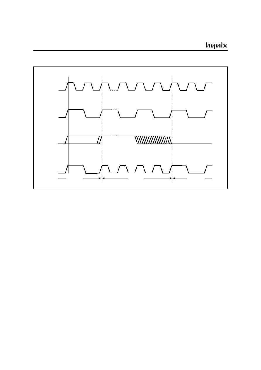
X2 MODE
The HMS99C5X core needs only 6 clock periods per machine cycle. This feature called "X2" provides the fol-
lowing advantages:
· Divide frequency crystals by 2 (cheaper crystals) while keeping same CPU power.
· Save power consumption while keeping same CPU power (oscillator power saving).
· Save power consumption by dividing dynamically operating frequency by 2 in operating and idle
modes.
· Increase CPU power by 2 while keeping same crystal frequency.
In order to keep the original C51 compatibility, a divider by 2 is inserted between the XTAL1 signal and the
main clock input of the core (phase generator). This divider may be disabled by software.
X2 Mode Description
The clock for the whole circuit and peripheral is first divided by two before being used by the CPU core and
peripherals. This allows any cyclic ratio to be accepted on XTAL1 input. In X2 mode, as this divider is bypassed,
the signals on XTAL1 must have a cyclic ratio between 40 to 60%. Figure 2. shows the clock generation block
diagram. X2 bit is validated on XTAL1
÷
2 rising edge to avoid glitches when switching from X2 to STD mode.
Figure 3.shows the mode switching waveforms:
Figure 2. Clock Generation Diagram
The X2 bit in the CKCON register allows to switch from 12 clock cycles per instruction to 6 clock cycles and
vice versa. At reset, the standard speed is activated (STD mode). Setting this bit activates the X2 feature(X2
mode).
CAUTION
In order to prevent any incorrect operation while operating in X2 mode, user must be aware that all peripherals
using clock frequency as time reference (UART, timers) will have their time reference divided by two. For ex-
ample a free running timer generating an interrupt every 30 ms will then generate an interrupt every 15 ms.
UART with 2400 baud rate will have 4800 baud rate.
f
OSC
÷
2
X2
State Machine: 6 clokc cyles
CKCON Register
1
0
CPU control
XTAL1
HMS99C5X Series
Jan. 2003 Ver 1.0
17
Figure 3. Mode Swithcing Waveforms
.
XTAL1
CPU Clock
XTAL1:2
X2 Mode
X2 bit
STD Mode
STD Mode
HMS99C5X Series
18
Jan. 2003 Ver 1.0
TIMER / COUNTER 0 AND 1
Timer/Counter 0 and 1 can be used in four operating modes as listed in Table 4:
In the "timer" function (C/T = "0") the register is incremented every machine cycle. Therefore the count rate is
f
OSC
/12.
In the "counter" function the register is incremented in response to a 1-to-0 transition at its corresponding exter-
nal input pin (P3.4/T0, P3.5/T1). Since it takes two machine cycles to detect a falling edge the max. count rate
is f
OSC
/24. External inputs INT0 and INT1 (P3.2, P3.3) can be programmed to function as a gate to facilitate
pulse width measurements. Figure 4 illustrates the input clock logic.
Figure 4. Timer/Counter 0 and 1 Input Clock Logic
Table 4. Timer/Counter 0 and 1 Operating Modes
Mode
Description
TMOD
Input Clock
Gate
C/T
M1
M0
internal
external (Max.)
0
8-bit timer/counter with a
divide-by-32 prescaler
X
X
0
0
f
OSC
÷
(12
×
32)
f
OSC
÷
(24
×
32)
1
16-bit timer/counter
X
X
0
1
f
OSC
÷
12
f
OSC
÷
24
2
8-bit timer/counter with
8-bit auto-reload
X
X
1
0
f
OSC
÷
12
f
OSC
÷
24
3
Timer/counter 0 used as
one 8-bit timer/counter and
one 8-bit timer Timer 1
stops
X
X
1
1
f
OSC
÷
12
f
OSC
÷
24
f
OSC
÷
12
TMOD
f
OSC
÷
12
P3.4/T0
P3.5/T1
Max. f
OSC
/24
C/T
=1
1
TCON
TR0 / 1
TMOD
Gate
&
P3.2 / INT0
P3.3 / INT1
Timer 0/1
Input Clock
0
1
HMS99C5X Series
Jan. 2003 Ver 1.0
19
TIMER 2
Timer 2 is a 16-bit timer/Counter with an up/down count feature. It can operate either as timer or as an event
counter which is selected by bit C/T2 (T2CON.1). It has three operating modes as shown in Table 5.
Note:
=
falling edge
Table 5. Timer/Counter 2 Operating Modes
Mode
T2CON
T2MOD T2CON
P1.1/
T2EX
Remarks
Input Clock
RCLK or
TCLK
CP/RL2
TR2
DCEN
EXEN2
internal
external
(P1.0/T2)
16-bit Auto-
Reload
0
0
0
0
0
0
0
0
1
1
1
1
0
0
1
1
0
1
X
X
X
0
1
reload upon over-
flow
reload trigger (fall-
ing edge)
Down counting
Up counting
f
OSC
÷
12
Max.
f
OSC
÷
24
16-bit
Capture
0
0
1
1
1
1
X
X
0
1
X
16 bit Timer/ Coun-
ter (only up-count-
ing)
capture TH2,TL2
RC2H,RC2L
f
OSC
÷
12
Max.
f
OSC
÷
24
Baud Rate
Generator
1
1
X
X
1
1
X
X
0
1
X
no overflow
interrupt request
(TF2)
extra external inter-
rupt ("Timer 2")
f
OSC
÷
12
Max.
f
OSC
÷
24
Off
X
X
0
X
X
X
Timer 2 stops
-
-
HMS99C5X Series
20
Jan. 2003 Ver 1.0
SERIAL INTERFACE (USART)
The serial port is full duplex and can operate in four modes (one synchronous mode, three asynchronous modes)
as illustrated in Table 6. The possible baud rates can be calculated using the formulas given in Table 7.
Table 6. USART Operating Modes
Mode
SCON
Baudrate
Description
SM0
SM1
0
0
0
Serial data enters and exits through RxD.
TxD outputs the shift clock. 8-bit are transmit-
ted/received (LSB first)
1
0
1
Timer 1/2 overflow rate
8-bit UART
10 bits are transmitted (through TxD) or
received (RxD)
2
1
0
or 9-bit
UART
11 bits are transmitted (TxD) or received (RxD)
3
1
1
Timer 1/2 overflow rate
9-bit UART
Like mode 2 except the variable baud rate
Table 7. Formulas for Calculating Baud rates
Baud Rate
derived from
Interface Mode
Baudrate
Oscillator
0
2
Timer 1 (16-bit timer)
(8-bit timer with
8-bit auto reload)
1,3
1,3
Timer 2
1,3
f
OSC
12
------------
f
OSC
32
------------
f
OSC
64
------------
f
OSC
12
------------
2
SMOD
64
------------------
f
OSC
×
2
SMOD
32
------------------
Timer 1 overflow
(
)
×
2
SMOD
32
------------------
f
OSC
12
256
TH1
(
)
Ð
[
]
×
----------------------------------------------------
×
f
OSC
32
65536
RC2H RC2L
,
(
)
Ð
[
]
×
-----------------------------------------------------------------------------------
HMS99C5X Series
Jan. 2003 Ver 1.0
21
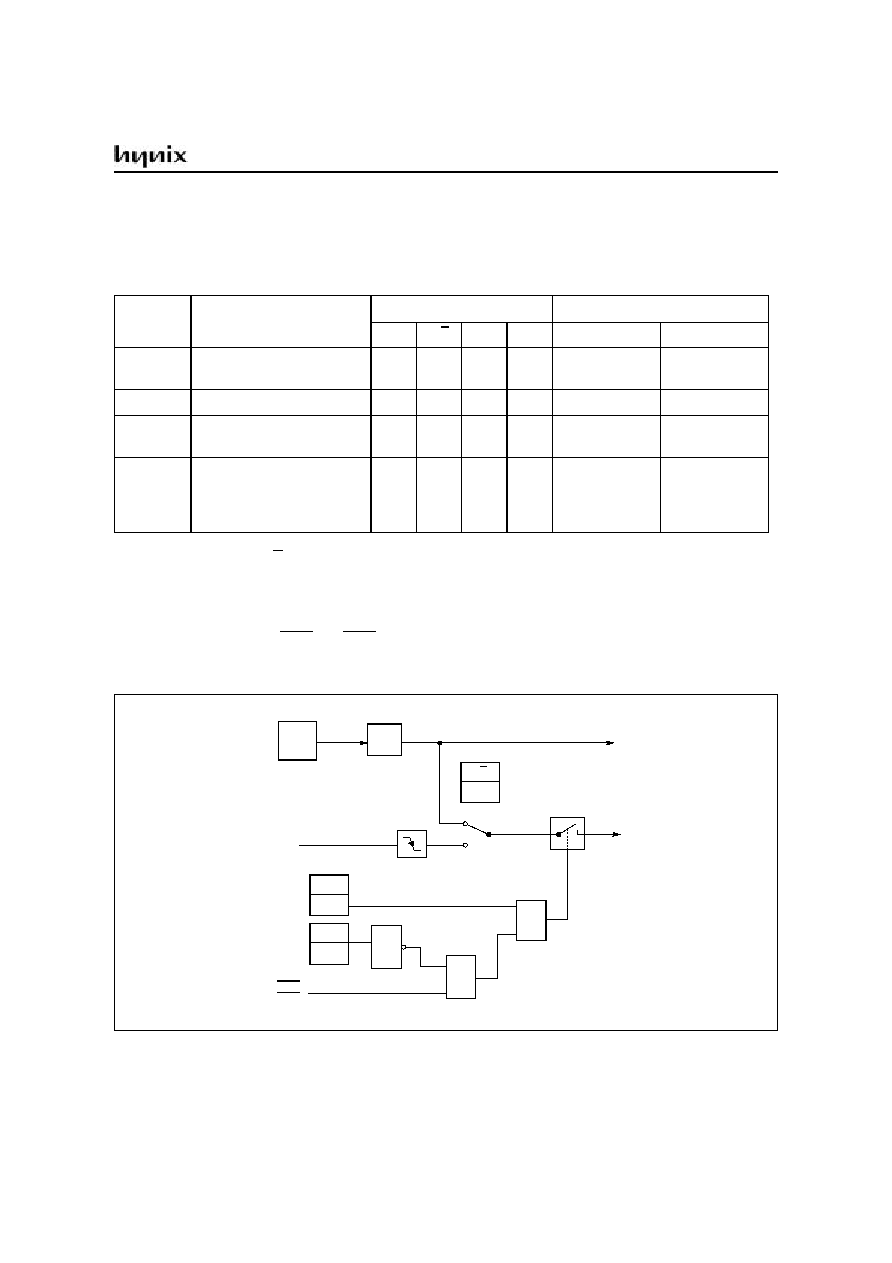
INTERRUPT SYSTEM
The HMS99C5X series provides 5 (4K bytes ROM version) or 6 (above 8K bytes ROM version) interrupt sourc-
es with two priority levels. Figure 5 gives a general overview of the interrupt sources and illustrates the request
and control flags.
Figure 5. Interrupt Request Sources
PT0
IP.1
PT1
IP.3
PT2
IP.5
PS
IP.4
PX0
IP.0
PX1
IP.2
EA
IE.7
ET0
IE.1
ET1
IE.3
ET2
IE.5
ES
IE.4
EX0
IE.0
EX1
IE.2
TF0
TCON.5
TF1
TCON.7
1
TF2
T2CON.7
EXF2
T2CON.6
1
RI
SCON.0
TI
SCON.1
IE0
TCON.1
IE1
TCON.3
IT0
TCON.0
IT1
TCON.2
P3.2/
INT0
P3.3/
INT1
EXEN2
T2CON.3
P1.1/
T2EX
Timer 2 Overflow
Timer 0 Overflow
Timer 1 Overflow
: Low level triggered
: Falling edge triggered
Low
Priority
High
Priority
UART
HMS99C5X Series
22
Jan. 2003 Ver 1.0
A low-priority interrupt can itself be interrupted by a high-priority interrupt, but not by another low priority in-
terrupt. A high-priority interrupt cannot be interrupted by any other interrupt source.
If two requests of different priority level are received simultaneously, the request of higher priority is serviced.
If requests of the same priority are received simultaneously, an internal polling sequence determines which re-
quest is serviced. Thus within each priority level there is a second priority structure determined by the polling
sequence as shown in Table 9.
Table 8. Interrupt Sources and their Corresponding Interrupt Vectors
Source (Request Flags)
Vectors
Vector Address
RESET
IE0
TF0
IE1
TF1
RI
+
TI
TF2
+
EXF2
RESET
External interrupt 0
Timer 0 interrupt
External interrupt 1
Timer 1 interrupt
Serial port interrupt
Timer 2 interrupt
0000H
0003H
000BH
0013H
001BH
0023H
002BH
Table 9. Interrupt Priority-Within-Level
Interrupt Source
Priority
External Interrupt 0
Timer 0 Interrupt
External Interrupt 1
Timer 1 Interrupt
Serial Channel
Timer 2 Interrupt
IE0
TF0
IE1
TF1
RI + TI
TF2 + EXF2
High
Low
HMS99C5X Series
Jan. 2003 Ver 1.0
23
Power Saving Modes
Two power down modes are available, the Idle Mode and Power Down Mode.
The bits PDE and IDLE of the register PCON select the Power Down mode or the Idle mode, respectively. If
the Power Down mode and the Idle mode are set at the same time, the Power Down mode takes precedence.
Table 10 gives a general overview of the power saving modes.
In the Power Down mode of operation, V
CC
can be reduced to minimize power consumption. It must be ensured,
however, that V
CC
is not reduced before the Power Down mode is invoked, and that V
CC
is restored to its normal
operating level, before the Power Down mode is terminated. The reset signal that terminates the Power Down
mode also restarts the oscillator. The reset should not be activated before V
CC
is restored to its normal operating
level and must be held active long enough to allow the oscillator to restart and stabilize (similar to power-on
reset).
Table 10. Power Saving Modes Overview
Mode
Entering
Instruction
Example
Leaving by
Remarks
Idle mode
ORL PCON, #01H
- Enabled interrupt
- Hardware Reset
CPU is gated off
CPU status registers maintain their
data.
Peripherals are active
Power-Down mode
ORL PCON, #02H
Hardware Reset
Oscillator is stopped, contents of on-
chip RAM and SFR's are maintained
(leaving Power Down Mode means
redefinition of SFR contents).

HMS99C5X Series
24
Jan. 2003 Ver 1.0
ELECTRICAL CHARACTERISTICS
Absolute Maximum Ratings
Ambient temperature under bias (T
A
)...................................................................................... -40 to + 85
°
C
Storage temperature (T
ST
)...................................................................................................... -65 to + 150
°
C
Voltage on V
CC
pins with respect to ground (V
SS
) ................................................................. -0.5V to 6.5V
Voltage on any pin with respect to ground (V
SS
) ..........................................................-0.5V to V
CC
+ 0.5V
Input current on any pin during overload condition............................................................-10mA to +10mA
Absolute sum of all input currents during overload condition...........................................................|100mA|
Power dissipation ............................................................................................................................... 200mW
Note: Stresses above those listed under "Absolute Maximum Ratings" may cause permanent damage of the de-
vice. This is a stress rating only and functional operation of the device at these or any other conditions above
those indicated in the operational sections of this specification is not implied. Exposure to absolute maximum rat-
ing conditions for longer periods may affect device reliability. During overload conditions (V
IN
> V
CC
or V
IN
< V
SS
)
the Voltage on V
CC
pins with respect to ground (V
SS
) must not exceed the values defined by the absolute maxi-
mum ratings.
HMS99C5X Series
Jan. 2003 Ver 1.0
25
DC Characteristics
DC Characteristics for HMS99C51/52
V
CC
= 5V + 10%, -15%; V
SS
=0V; T
A
= -40
°
C to 85
°
C
Parameter
Symbol
Limit Values
Un
it
Test Conditions
Min.
Max.
Input low voltage
(except EA, RESET)
V
IL
-0.5
0.2V
CC
- 0.1
V
V
CC
= 5.5V
Input low voltage (EA)
V
IL1
-0.5
0.2V
CC
- 0.1
V
V
CC
= 5.5V
Input low voltage (RESET)
V
IL2
-0.5
0.2V
CC
+ 0.1
V
V
CC
= 5.5V
Input high voltage (except
XTAL1, EA, RESET)
V
IH
0.2V
CC
+
0.9
V
CC
+ 0.5
V
V
CC
= 4.5V
Input high voltage to XTAL1
V
IH1
0.7V
CC
V
CC
+ 0.5
V
V
CC
= 4.5V
Input high voltage to EA,
RESET
V
IH2
0.6V
CC
V
CC
+ 0.5
V
V
CC
= 4.5V
Output low voltage
(ports 1, 2, 3)
V
OL
-
0.45
V
V
CC
= 5.5V, I
OL
= 1.6mA
1)
Output low voltage
(port 0, ALE, PSEN)
V
OL1
-
0.45
V
V
CC
= 5.5V, I
OL
= 3.2mA
1)
Output high voltage
(ports 1, 2, 3)
V
OH
2.4
0.9V
CC
-
V
V
CC
= 4.5V, I
OH
= -80
µ
A
V
CC
= 4.5V, I
OH
= -10
µ
A
Output high voltage
(port 0 in external bus
mode, ALE, PSEN)
V
OH1
2.4
0.9V
CC
-
V
V
CC
= 4.5V, I
OH
= -800
µ
A
2)
V
CC
= 4.5V, I
OH
= -80
µ
A
2)
Logic 0 input current
(ports 1, 2, 3)
I
IL
-10
-65
µ
A
V
IN
= 0.45V
Logical 1-to-0 transition cur-
rent (ports 1, 2, 3)
I
TL
-65
-650
µ
A
V
IN
= 2.0V
Input leakage current
(port 0, EA)
I
LI
-
±
1
µ
A
0.45
<
V
IN
<
V
CC
Pin capacitance
C
IO
-
10
pF
f
C
= 1MHz
T
A
= 25
°
C
Power supply current:
Active mode, 4MHz
3)
Idle mode, 4MHz
4)
Active mode, 24 MHz
4)
Idle mode, 24MHz
4)
Active mode, 40 MHz
4)
Idle mode, 40 MHz
4)
Power Down Mode
4)
I
CC
I
CC
I
CC
I
CC
I
CC
I
CC
I
PD
-
8
4
25
10
30
15
50
mA
A
mA
mA
mA
mA
mA
µ
A
V
CC
= 5V
4)
V
CC
= 5V
5)
V
CC
= 5V
7)
V
CC
= 5V
8)
V
CC
= 5V
7)
V
CC
= 5V
8)
V
CC
= 5V
6)

HMS99C5X Series
26
Jan. 2003 Ver 1.0
1) Capacitive loading on ports 0 and 2 may cause spurious noise pulses to be superimposed on the V
OL
of ALE and port 3.
The noise is due to external bus capacitance discharging into the port 0 and port 2 pins when these pins make 1-to-0 tran-
sitions during bus operation. In the worst case (capacitive loading:
>
50pF at 3.3V,
>
100pF at 5V), the noise pulse on ALE
line may exceed 0.8V. In such cases it may be desirable to qualify ALE with a schmitt-trigger, or use an address latch with
a schmitt-trigger strobe input.
2) Capacitive loading on ports 0 and 2 may cause the V
OH
on ALE and PSEN to momentarily fall below the 0.9V
CC
specifica-
tion when the address lines are stabilizing.
3) I
CC
Max at other frequencies is given by:
active mode: I
CC
= 1.27
×
f
OSC
+ 5.73
idle mode: I
CC
= 0.28
×
f
OSC
+ 1.45 (except OTP devices)
where f
OSC
is the oscillator frequency in MHz. I
CC
values are given in mA and measured at V
CC
= 5V.
4) I
CC
(active mode) is measured with:
XTAL1 driven with t
CLCH
, t
CHCL
= 5ns, V
IL
= V
SS
+ 0.5V, V
IH
= V
CC
- 0.5V; XTAL2 = N.C.;
EA = Port0 = RESET = V
CC
; all other pins are disconnected. I
CC
would be slightly higher if a crystal oscillator is used (appr.
1mA).
5) I
CC
(Idle mode) is measured with all output pins disconnected and with all peripherals disabled;
XTAL1 driven with t
CLCH
, t
CHCL
= 5ns, V
IL
= V
SS
+ 0.5V, V
IH
= V
CC
- 0.5V; XTAL2 = N.C.;
RESET = EA = V
SS
; Port0 = V
CC
; all other pins are disconnected;
6) I
PD
(Power Down Mode) is measured under following conditions:
EA = Port0 = V
CC
; RESET = V
SS
; XTAL2 = N.C.; XTAL1 = V
SS
; all other pins are disconnected.
HMS99C5X Series
Jan. 2003 Ver 1.0
27
AC Characteristics
Explanation of the AC Symbols
Each timing symbol has 5 characters. The first character is always a `t' (stand for time). The other characters,
depending on their positions, stand for the name of a signal or the logical status of that signal. The following is
a list of all the characters and what they stand for.
AC Characteristics for HMS99C5X series (12MHz version)
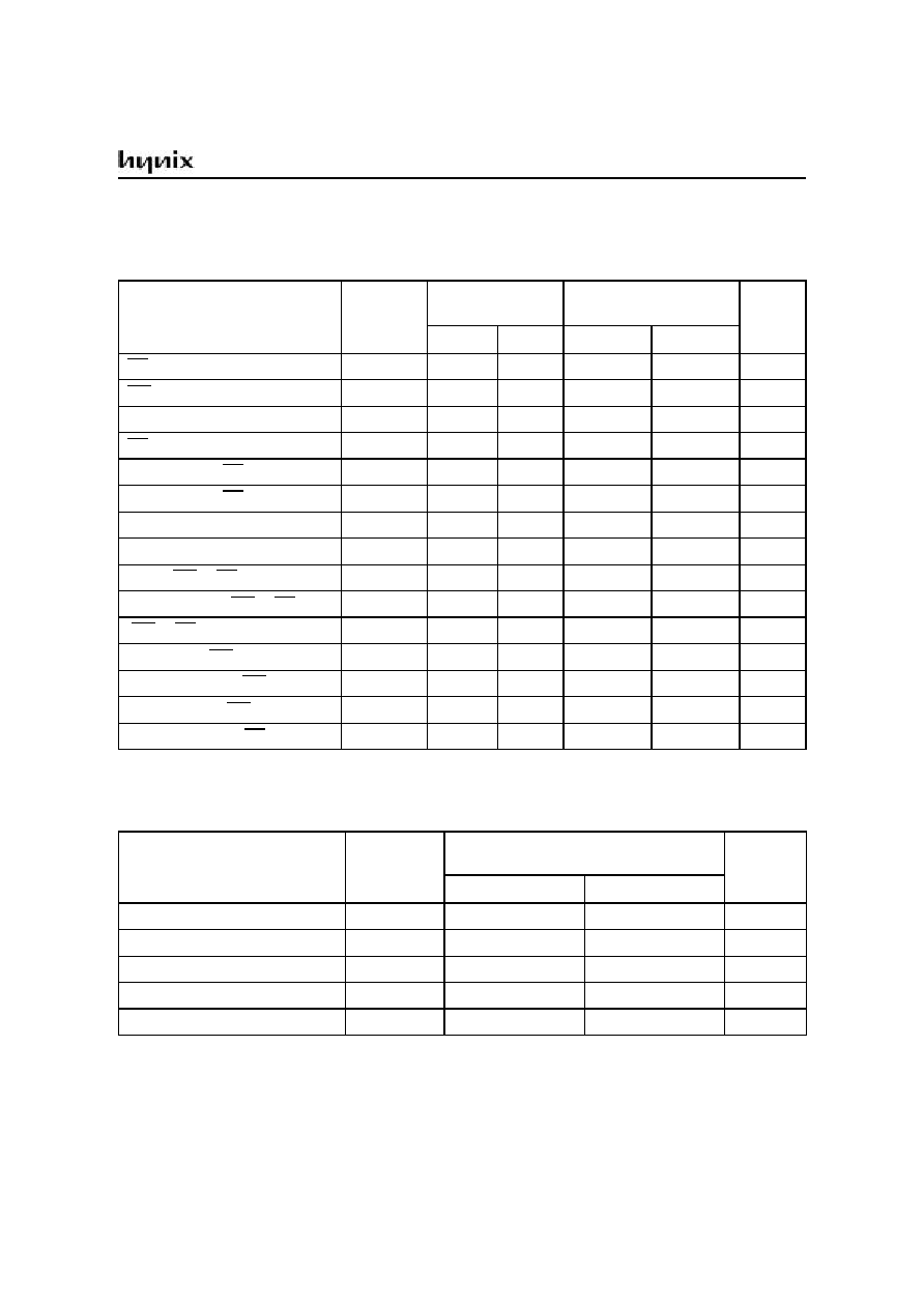
External Program Memory Characteristics
Interfacing the HMS99C5X series to devices with float times up to 75 ns is permissible. This limited bus contention will not
cause any damage to port 0 Drivers.
V
CC
= 5V :
V
CC
= 5V
+
10%,
-
15%; V
SS
= 0V; T
A
= -40
°
C to 85
°
C
(C
L
for port 0. ALE and PSEN outputs = 100pF; C
L
for all other outputs = 80pF)
Variable clock :
Vcc = 5V : 1/t
CLCL
= 3.5 MHz to 12 MHz
Parameter
Symbol
12 MHz Oscillator
Variable Oscillator
1/t
CLCL
= 3.5 to 12MHz
Unit
Min.
Max.
Min.
Max.
ALE pulse width
t
LHLL
127
-
2t
CLCL
-40
-
ns
Address setup to ALE
t
AVLL
43
-
t
CLCL
-40
-
ns
Address hold after ALE
t
LLAX
30
-
t
CLCL
-53
-
ns
ALE low to valid instruction in
t
LLIV
-
233
-
4t
CLCL
-100
ns
ALE to PSEN
t
LLPL
58
-
t
CLCL
-25
-
ns
PSEN pulse width
t
PLPH
215
-
3t
CLCL
-35
-
ns
PSEN to valid instruction in
t
PLIV
-
150
-
3t
CLCL
-100
ns
Input instruction hold after PSEN
t
PXIX
0
-
0
-
ns
Input instruction float after PSEN
t
PXIZ
-
63
-
t
CLCL
-20
ns
Address valid after PSEN
t
PXAV
75
-
t
CLCL
-8
-
ns
Address to valid instruction in
t
AVIV
-
302
-
5t
CLCL
-115
ns
Address float to PSEN
t
AZPL
0
-
0
-
ns
A: Address
C: Clock
D: Input Data
H: Logic level HIGH
I: Instruction (program memory contents)
L: Logic level LOW, or ALE
P: PSEN
Q: Output Data
R: RD signal
T: Time
V: Valid
W: WR signal
X: No longer a valid logic level
Z: Float
For example,
t
AVLL
= Time from Address Valid to ALE Low
t
LLPL
= Time from ALE Low to PSEN Low

HMS99C5X Series
28
Jan. 2003 Ver 1.0
AC Characteristics for HMS99C5X series (12MHz)
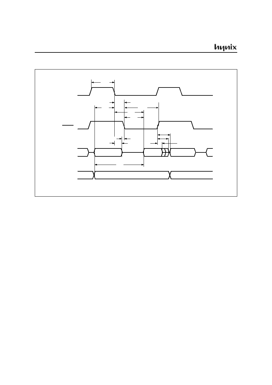
External Data Memory Characteristics
Advance Information (12MHz)
External Clock Drive
Parameter
Symbol
12 MHz Oscillator
Variable Oscillator
1/t
CLCL
= 3.5 to 12MHz
Unit
Min.
Max.
Min.
Max.
RD pulse width
t
RLRH
400
-
6t
CLCL
-100
-
ns
WR pulse width
t
WLWH
400
-
6t
CLCL
-100
-
ns
Address hold after ALE
t
LLAX2
53
-
t
CLCL
-30
-
ns
RD to valid data in
t
RLDV
-
252
-
5t
CLCL
-165
ns
Data hold after RD
t
RHDX
0
-
0
-
ns
Data float after RD
t
RHDZ
-
97
-
2t
CLCL
-70
ns
ALE to valid data in
t
LLDV
-
517
-
8t
CLCL
-150
ns
Address to valid data in
t
AVDV
-
585
-
9t
CLCL
-165
ns
ALE to WR or RD
t
LLWL
200
300
3t
CLCL
-50
3t
CLCL
+50
ns
Address valid to WR or RD
t
AVWL
203
-
4t
CLCL
-130
-
ns
WR or RD high to ALE high
t
WHLH
43
123
t
CLCL
-40
t
CLCL
+40
ns
Data valid to WR transition
t
QVWX
33
-
t
CLCL
-50
-
ns
Data setup before WR
t
QVWH
433
-
7t
CLCL
-150
-
ns
Data hold after WR
t
WHQX
33
-
t
CLCL
-50
-
ns
Address float after RD
t
RLAZ
-
0
-
0
ns
Parameter
Symbol
Variable Oscillator
(Freq. = 3.5 to 12MHz)
Unit
Min.
Max.
Oscillator period (V
CC
=5V)
t
CLCL
83.3
285.7
ns
High time
t
CHCX
20
t
CLCL
- t
CLCX
ns
Low time
t
CLCX
20
t
CLCL
- t
CHCX
ns
Rise time
t
CLCH
-
20
ns
Fall time
t
CHCL
-
20
ns
HMS99C5X Series
Jan. 2003 Ver 1.0
29
AC Characteristics for HMS99C5X series (24MHz version)
V
CC
= 5V + 10%,
-
15%; V
SS
= 0V; T
A
= -40
°
C to 85
°
C
(C
L
for port 0. ALE and PSEN outputs = 100pF; C
L
for all other outputs = 80pF)
External Program Memory Characteristics
Interfacing the HMS99C5X series to devices with float times up to 35 ns is permissible. This limited bus contention will not
cause any damage to port 0 Drivers.
Parameter
Symbol
24 MHz Oscillator
Variable Oscillator
1/t
CLCL
= 3.5 to 24MHz
Unit
Min.
Max.
Min.
Max.
ALE pulse width
t
LHLL
43
-
2t
CLCL
-40
-
ns
Address setup to ALE
t
AVLL
17
-
t
CLCL
-25
-
ns
Address hold after ALE
t
LLAX
17
-
t
CLCL
-25
-
ns
ALE low to valid instruction in
t
LLIV
-
80
-
4t
CLCL
-87
ns
ALE to PSEN
t
LLPL
22
-
t
CLCL
-20
-
ns
PSEN pulse width
t
PLPH
95
-
3t
CLCL
-30
-
ns
PSEN to valid instruction in
t
PLIV
-
60
-
3t
CLCL
-65
ns
Input instruction hold after PSEN
t
PXIX
0
-
0
-
ns
Input instruction float after PSEN
t
PXIZ
-
32
-
t
CLCL
-10
ns
Address valid after PSEN
t
PXAV
37
-
t
CLCL
-5
-
ns
Address to valid instruction in
t
AVIV
-
148
-
5t
CLCL
-60
ns
Address float to PSEN
t
AZPL
0
-
0
-
ns

HMS99C5X Series
30
Jan. 2003 Ver 1.0
AC Characteristics for HMS99C5X series (24MHz)
External Data Memory Characteristics
Advance Information (24MHz)
External Clock Drive
Parameter
Symbol
24 MHz Oscillator
Variable Oscillator
1/t
CLCL
= 3.5 to 24MHz
Unit
Min.
Max.
Min.
Max.
RD pulse width
t
RLRH
180
-
6t
CLCL
-70
-
ns
WR pulse width
t
WLWH
180
-
6t
CLCL
-70
-
ns
Address hold after ALE
t
LLAX2
15
-
t
CLCL
-27
-
ns
RD to valid data in
t
RLDV
-
118
-
5t
CLCL
-90
ns
Data hold after RD
t
RHDX
0
-
0
-
ns
Data float after RD
t
RHDZ
-
63
-
2t
CLCL
-20
ns
ALE to valid data in
t
LLDV
-
200
-
8t
CLCL
-133
ns
Address to valid data in
t
AVDV
-
220
-
9t
CLCL
-155
ns
ALE to WR or RD
t
LLWL
75
175
3t
CLCL
-50
3t
CLCL
+50
ns
Address valid to WR or RD
t
AVWL
67
-
4t
CLCL
-97
-
ns
WR or RD high to ALE high
t
WHLH
17
67
t
CLCL
-25
t
CLCL
+25
ns
Data valid to WR transition
t
QVWX
5
-
t
CLCL
-37
-
ns
Data setup before WR
t
QVWH
170
-
7t
CLCL
-122
-
ns
Data hold after WR
t
WHQX
15
-
t
CLCL
-27
-
ns
Address float after RD
t
RLAZ
-
0
-
0
ns
Parameter
Symbol
Variable Oscillator
(Freq. = 3.5 to 24MHz)
Unit
Min.
Max.
Oscillator period
t
CLCL
41.7
285.7
ns
High time
t
CHCX
12
t
CLCL
- t
CLCX
ns
Low time
t
CLCX
12
t
CLCL
- t
CHCX
ns
Rise time
t
CLCH
-
12
ns
Fall time
t
CHCL
-
12
ns

HMS99C5X Series
Jan. 2003 Ver 1.0
31
AC Characteristics for HMS99C5X series (40MHz version)
V
CC
= 5V + 10%,
-
15%; V
SS
= 0V; T
A
= -40
°
C to 85
°
C
(C
L
for port 0. ALE and PSEN outputs = 100pF; C
L
for all other outputs = 80pF)
External Program Memory Characteristics
Interfacing the HMS99C5X series to devices with float times up to 20 ns is permissible. This limited bus contention will not
cause any damage to port 0 Drivers.
Parameter
Symbol
40 MHz Oscillator
Variable Oscillator
1/t
CLCL
= 3.5 to 40MHz
Unit
Min.
Max.
Min.
Max.
ALE pulse width
t
LHLL
40
-
2t
CLCL
-
20
-
ns
Address setup to ALE
t
AVLL
10
-
t
CLCL
-
20
-
ns
Address hold after ALE
t
LLAX
10
-
t
CLCL
-20
-
ns
ALE low to valid instruction in
t
LLIV
-
56
-
4t
CLCL
-
65
ns
ALE to PSEN
t
LLPL
15
-
t
CLCL
-
15
-
ns
PSEN pulse width
t
PLPH
80
-
3t
CLCL
-
20
-
ns
PSEN to valid instruction in
t
PLIV
-
35
-
3t
CLCL
-
55
ns
Input instruction hold after PSEN
t
PXIX
0
-
0
-
ns
Input instruction float after PSEN
t
PXIZ
-
20
-
t
CLCL
-
10
ns
Address valid after PSEN
t
PXAV
25
-
t
CLCL
-
5
-
ns
Address to valid instruction in
t
AVIV
-
91
-
5t
CLCL
-
60
ns
Address float to PSEN
t
AZPL
0
-
0
-
ns
HMS99C5X Series
32
Jan. 2003 Ver 1.0
AC Characteristics for HMS99C5X series (40MHz)
External Data Memory Characteristics
Advance Information (40MHz)
External Clock Drive
Parameter
Symbol
at 40 MHz Clock
Variable Clock
1/t
CLCL
= 3.5 to 40MHz
Unit
Min.
Max.
Min.
Max.
RD pulse width
t
RLRH
132
-
6t
CLCL
-50
-
ns
WR pulse width
t
WLWH
132
-
6t
CLCL
-50
-
ns
Address hold after ALE
t
LLAX2
10
-
t
CLCL
-20
-
ns
RD to valid data in
t
RLDV
-
81
-
5t
CLCL
-70
ns
Data hold after RD
t
RHDX
0
-
0
-
ns
Data float after RD
t
RHDZ
-
46
-
2t
CLCL
-15
ns
ALE to valid data in
t
LLDV
-
153
-
8t
CLCL
-90
ns
Address to valid data in
t
AVDV
-
183
-
9t
CLCL
-90
ns
ALE to WR or RD
t
LLWL
71
111
3t
CLCL
-20
3t
CLCL
+20
ns
Address valid to WR or RD
t
AVWL
66
-
4t
CLCL
-55
-
ns
WR or RD high to ALE high
t
WHLH
10
40
t
CLCL
-20
t
CLCL
+20
ns
Data valid to WR transition
t
QVWX
5
-
t
CLCL
-25
-
ns
Data setup before WR
t
QVWH
142
-
7t
CLCL
-70
-
ns
Data hold after WR
t
WHQX
10
-
t
CLCL
-20
-
ns
Address float after RD
t
RLAZ
-
0
-
0
ns
Parameter
Symbol
Variable Oscillator
(Freq. = 3.5 to 40MHz)
Unit
Min.
Max.
Oscillator period
t
CLCL
30.3
285.7
ns
High time
t
CHCX
11.5
t
CLCL
- t
CLCX
ns
Low time
t
CLCX
11.5
t
CLCL
- t
CHCX
ns
Rise time
t
CLCH
-
5
ns
Fall time
t
CHCL
-
5
ns
HMS99C5X Series
Jan. 2003 Ver 1.0
33
Figure 6. External Program Memory Read Cycle
t
LHLL
t
PXAV
t
PXIZ
t
PXIX
t
LLAX
t
LLIV
t
PLIV
t
PLPH
t
AZPL
t
LLPL
t
AVLL
A0-A7
INSTR.
IN
A0-A7
A8-A15
A8-A15
t
AVIV
ALE
PSEN
PORT 0
PORT 2
HMS99C5X Series
34
Jan. 2003 Ver 1.0
Figure 7. External Data Memory Read Cycle
Figure 8. External Data Memory Write Cycle
t
LHLL
P2.0-P2.7 or A8-A15 from DPH
A8-A15 from PCH
ALE
PSEN
PORT 0
PORT 2
RD
t
LLWL
DATA IN
A0-A7 from PCL
INSTR. IN
A0-A7 from
t
LLAX2
t
AVWL
t
AVLL
t
AVDV
t
RLAZ
t
LLDV
t
RLRH
t
RLDV
t
RHDX
t
RHDZ
t
WHLH
RI or DPL
t
LHLL
P2.0-P2.7 or A8-A15 from DPH
A8-A15 from PCH
ALE
PSEN
PORT 0
PORT 2
WR
t
LLWL
DATA OUT
A0-A7 from PCL
INSTR. IN
A0-A7 from
t
LLAX2
t
AVWL
t
AVLL
t
WLWH
t
WHQX
t
WHLH
RI or DPL
t
QVWX
t
QVWH
HMS99C5X Series
Jan. 2003 Ver 1.0
35
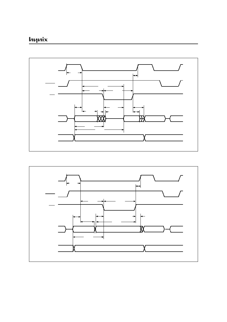
Figure 9. AC Testing: Input, Output Waveforms
Figure 10. Float Waveforms
Figure 11. External Clock Cycle
AC Inputs during testing are driven at V
CC
-
0.5V for a logic `1' and 0.45V for a logic `0'.
0.2V
CC
+
0.9
0.2V
CC
-
0.1
Test Points
V
CC
-
0.5V
0.45V
Timing measurements are made a V
IHmin
for a logic `1' and V
ILmax
for a logic `0'.
V
LOAD
+
0.1
V
LOAD
-
0.1
Timing Reference Points
0.2V
CC
-
0.1
V
OH
-
0.1
V
OL
+
0.1
V
LOAD
For timing purposes a port pin is no longer floating when a 100mV change from load voltage
I
OL
/ I
OH
20mA.
occurs and begins to float when a 100mV change from the loaded V
OH
/ V
OL
level occurs.
t
CHCL
t
CLCH
t
CHCX
t
CLCL
t
CLCX
0.2 V
CC
-
0.1
0.7 V
CC
V
CC
-
0.5V
0.45V
HMS99C5X Series
36
Jan. 2003 Ver 1.0
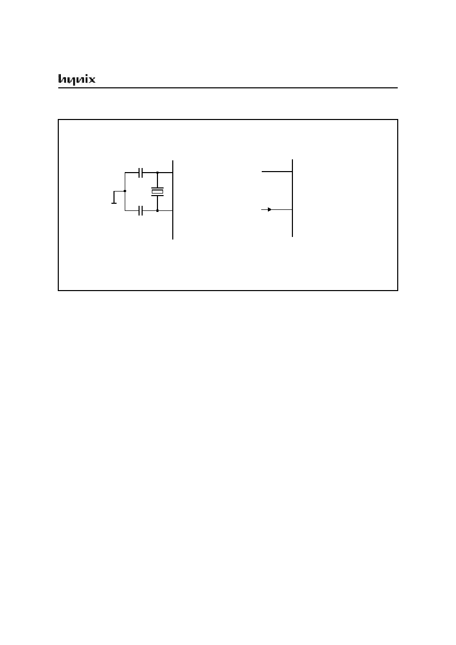
OSCILLATOR CIRCUIT
Figure 12. Recommended Oscillator Circuits
Oscillation circuit is designed to be used either with a ceramic resonator or crystal oscillator. Since each crystal
and ceramic resonator have their own characteristics, the user should consult the crystal manufacturer for ap-
propriate values of external components.
XTAL2
P-LCC-44/Pin 20
P-DIP-40/Pin 18
M-QFP-44/Pin 14
XTAL1
P-LCC-44/Pin 21
P-DIP-40/Pin 19
M-QFP-44/Pin 15
CRYSTAL OSCILLATOR MODE
DRIVING FROM EXTERNAL SOURCE
XTAL2
P-LCC-44/Pin 20
P-DIP-40/Pin 18
M-QFP-44/Pin 14
XTAL1
P-LCC-44/Pin 21
P-DIP-40/Pin 19
M-QFP-44/Pin 15
External Oscillator
Signal
N.C.
C2
C1
C1, C2 = 30pF
±
10pF for Crystals
For Ceramic Resonators, contact resonator manufacturer.
HMS99C5X Series
Jan. 2003 Ver 1.0
37
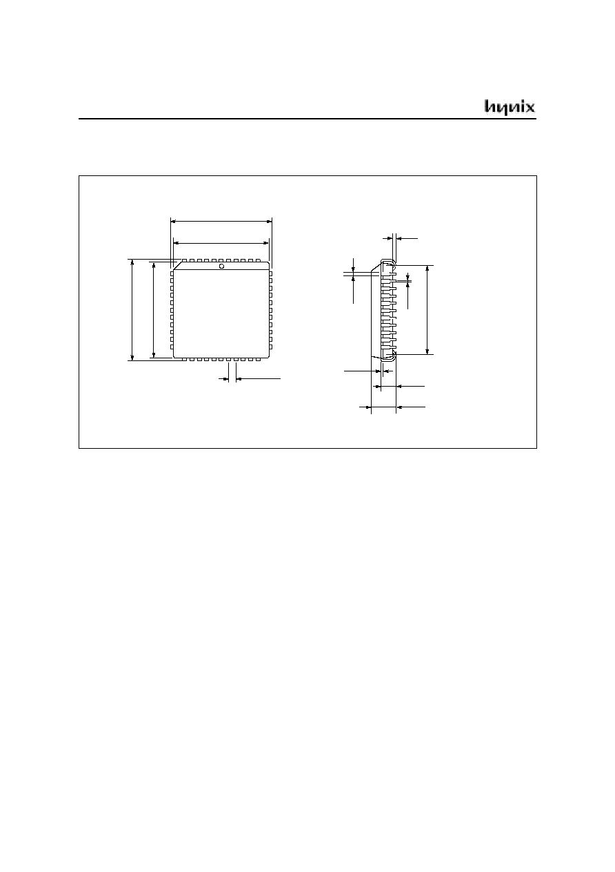
Plastic Package P-LCC-44
(Plastic Leaded Chip-Carrier)
0.180
0.165
UNIT: INCH
44PLCC
0.012
0.0075
0.120
0.090
0.
032
0.
026
0.63
0
0.59
0
min. 0.020
0.656
0.650
0.695
0.685
0.
656
0.
650
0.
695
0.
685
0.050 BSC
0.
0
2
1
0.
0
1
3
HMS99C5X Series
38
Jan. 2003 Ver 1.0
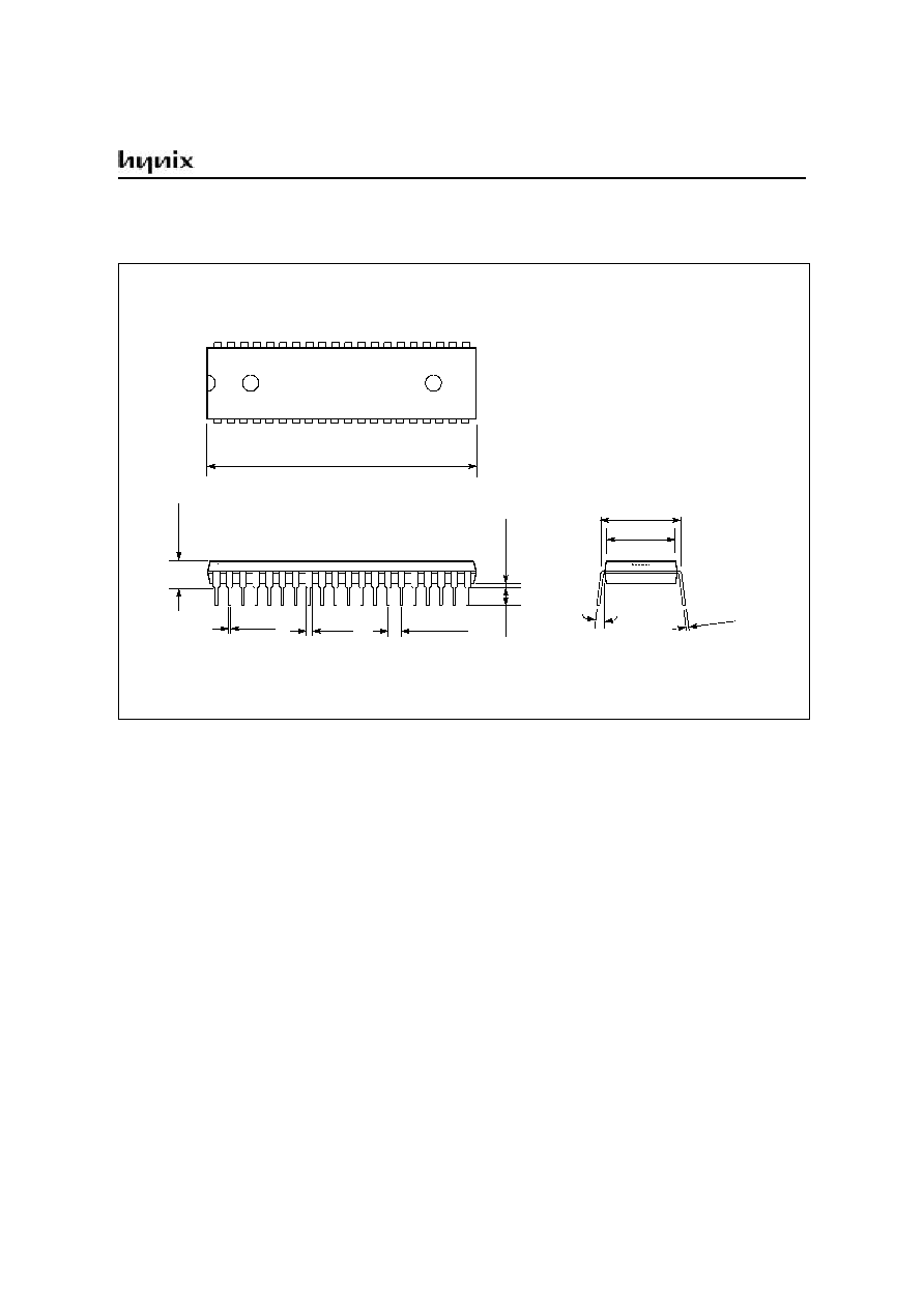
Plastic Package P-DIP-40
(Plastic Dual in-Line Package)
UNIT: INCH
2.075
2.045
0
.
20
0 m
a
x
.
0.022
0.015
0.065
0.045
0.100 BSC
0.550
0.530
0.600 BSC
0-15
°
0.012
0.008
40DIP
0.
1
4
0
0.
1
2
0
mi
n
.
0.
015
HMS99C5X Series
Jan. 2003 Ver 1.0
39
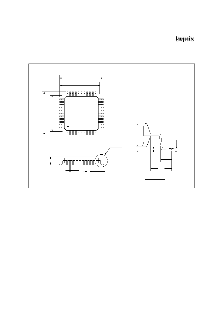
Plastic Package P-MPQF-44
(Plastic Metric Quad Flat Package)
2.35 max.
SEE DETAIL "A"
1.03
0.73
0-7
°
0.2
5
0.1
0
1.60
REF
DETAIL "A"
UNIT: MM
0.45
0.30
0.80 BSC
2.
1
0
1.
9
5
44MQFP
0
.
1
3
0
.
2
3
10.10
9.90
13.45
12.95
10
.10
9.
90
13
.45
12
.95
Document Outline