Äîêóìåíòàöèÿ è îïèñàíèÿ www.docs.chipfind.ru
HY51V(S)17403HG/HGL
4M x 4Bit EDO DRAM
This document is a general product description and is subject to change without notice. Hyundai Electronics does not assume any
responsibility for use of circuits described. No patent licenses are implied.
Rev.0.1/Apr.01
DESCRIPTION
FEATURES
·
Fast access time and cycle time
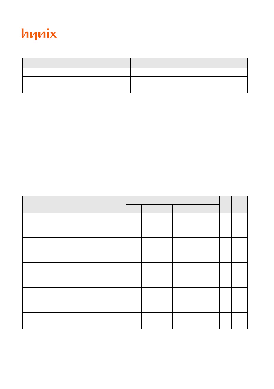
ORDERING INFORMATION
Part No
tRAC
tCAC
tRC
tHPC
HY51V(S)17403HG/HGL-5
50ns
13ns
84ns
20ns
HY51V(S)17403HG/HGL-6
60ns
15ns
104ns
25ns
HY51V(S)17403HG/HGL-7
70ns
18ns
124ns
30ns
50ns
60ns
70ns
Active
432mW
369mW
360mW
Standby
7.2mW(CMOS level Max)
0.36mW (L-version : Max)
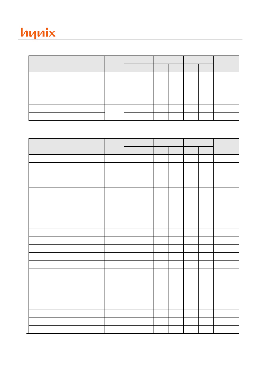
Part Number
Access Time
Package
HY51V(S)17403HGJ/HG(L)J-5
HY51V(S)17403HGJ/HG(L)J-6
HY51V(S)17403HGJ/HG(L)J-7
50ns
60ns
70ns
300mil 24(26)pin SOJ
HY51V(S)17403HGT/HG(L)T-5
HY51V(S)17403HGT/HG(L)T-6
HY51V(S)17403HGT/HG(L)T-7
50ns
60ns
70ns
300mil 24(26)pin TSOP-II
PRELIMINARY
The HY51V(S)17403HG/HGL is the new generation dynamic RAM organized 4,194,304 words x 4bit.
HY51V(S)17403HG/HGL has realized higher density, higher performance and various functions by utiliz-
ing advanced CMOS process technology. The HY51V(S)17403HG/HGL offers Extended Data Out Page-
Mode as a high speed access mode. Multiplexed address inputs permit the HY51V(S)17403HG/HGL to be
packaged in standard 300mil 24(26)pin SOJ and 24(26) pin TSOP-II. The package size provides high sys-
tem bit densities and is compatible with widely available automated testing and insertion equipment.
System oriented features include single power supply 3.3V +/- 0.3V tolerance, direct interfacing capability
with high performance logic families such as Schottky TTL.
·
Extended Data Out Mode capability
·
Read-modify-write capability
·
Multi-bit parallel test capability
·
TTL(3.3V) compatible inputs and outputs
·
/RAS only, CAS-before-/RAS, Hidden and self
refresh(L-version) capability
·
JEDEC standard pinout
·
24(26)pin plastic SOJ / 24(26)pin TSOP-II
·
Single power supply of 3.3V +/- 0.3V
·
Battery back up operation(L-version)
·
Power dissipation
·
Refresh cycle
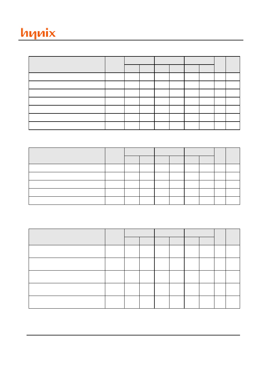
Part No
Ref
Normal
L-part
HY51V17403HG
2K
32ms
HY51V17403HGL
2K
128ms
(S) : Self refresh, (L) : Low power
HY51V(S)17403HG/HGL
Rev.0.1/Apr.01
2
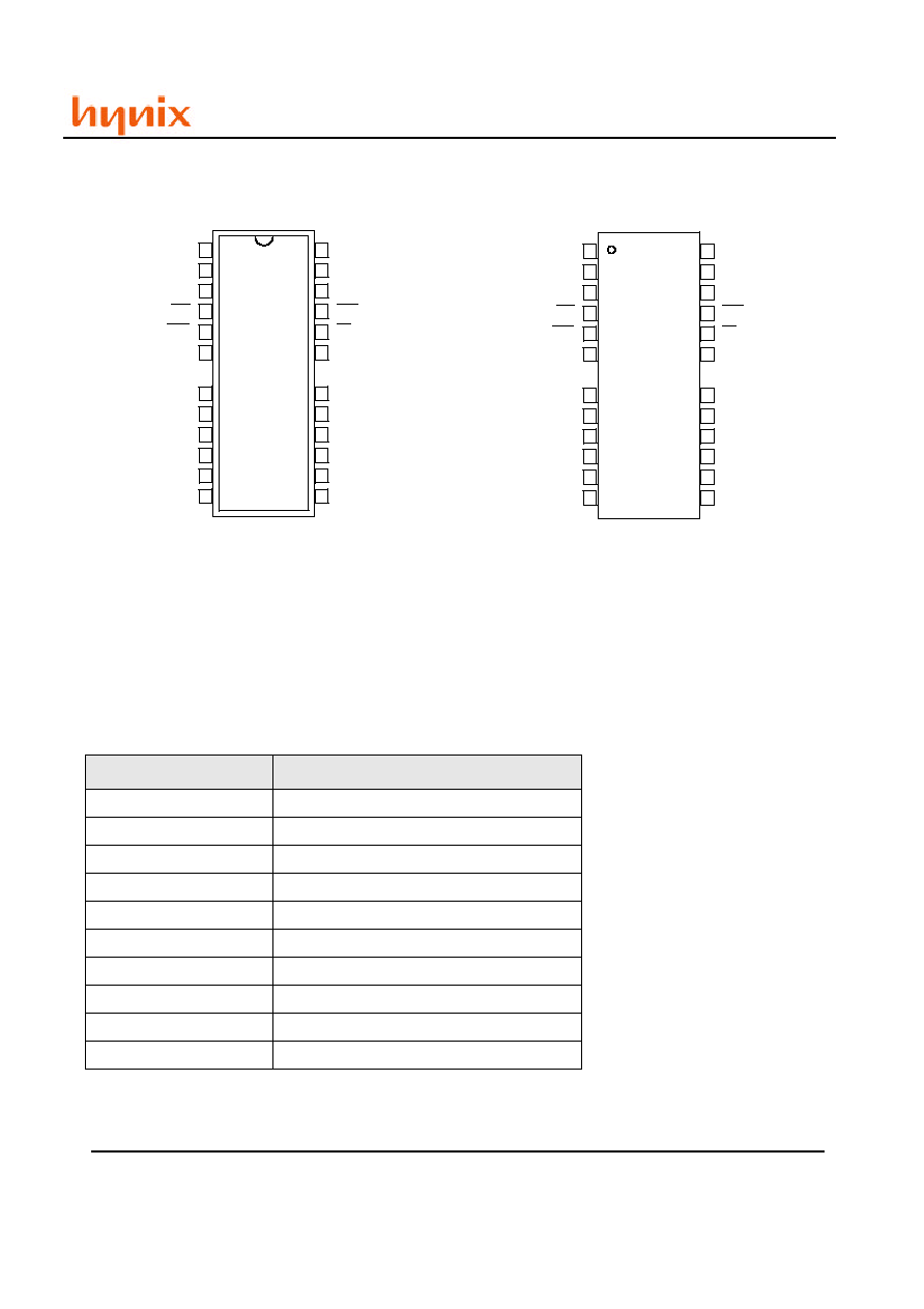
PIN CONFIGURATION
Pin
Function
/RAS
Row Address Strobe
/CAS
Column Address Strobe
/WE
Write Enable
/OE
Output Enable
A0-A11
Address Inputs
A0-A11
Refresh Address Inputs
I/O 1- I/O 4
Data Input / Output
Vcc
Power (3.3V)
Vss
Ground
NC
No connection
PIN DESCRIPTION
V
CC
I/O1
I/O2
WE
RAS
A11
A10
A0
A1
A2
A3
V
CC
V
SS
I/O4
I/O3
CAS
OE
A9
A8
A7
A6
A5
A4
V
SS
1
2
3
4
5
6
8
9
10
11
12
13
14
15
16
17
18
19
21
22
23
24
25
26
24(26) Pin Plastic SOJ
V
CC
I/O1
I/O2
WE
RAS
A11
A10
A0
A1
A2
A3
V
CC
V
SS
I/O4
I/O3
CAS
OE
A9
A8
A7
A6
A5
A4
V
SS
1
2
3
4
5
6
8
9
10
11
12
13
14
15
16
17
18
19
21
22
23
24
25
26
24(26) Pin Plastic TSOP-II
HY51V(S)17403HG/HGL
Rev.0.1/Apr.01
3
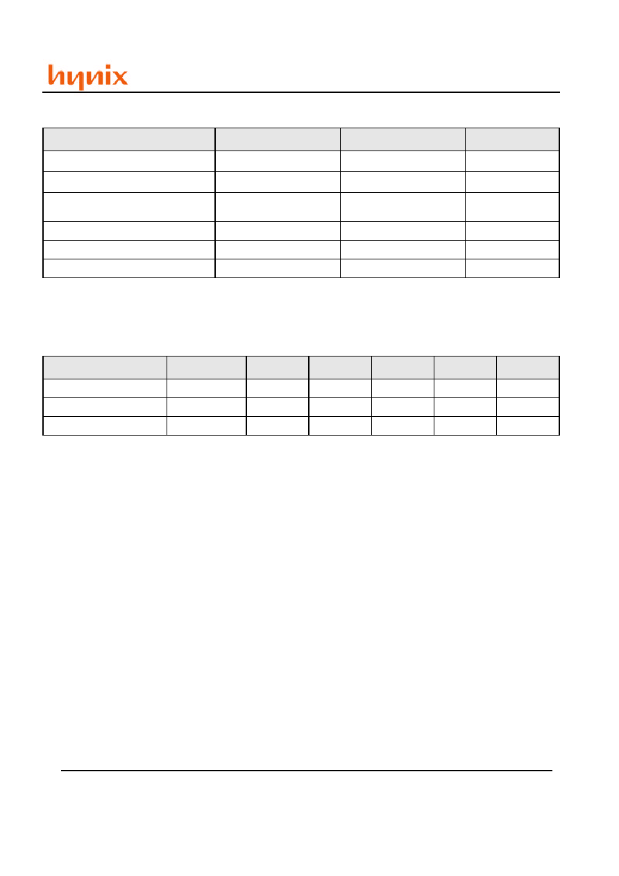
ABSOLUTE MAXIMUM RATINGS
Recommended DC OPERATING CONDITIONS
(TA=0 to 70
o
C)
Note : All voltages are referenced to Vss
Parameter
Symbol
Rating
Unit
Ambient Temperature
T
A
0 ~ 70
o
C
Storage Temperature
T
STG
-55 ~ 125
o
C
Voltage on Any Pin relative to V
ss
V
T
-0.5 ~ Vcc + 0.5
(Max 4.6V)
V
Voltage on V
cc
relative to V
ss
V
cc
-0.5 ~ 4.6
V
Short Circuit Output Current
I
OUT
50
mA
Power Dissipation
P
T
1
W
Parameter
Symbol
Min
Typ.
Max
Unit
Note
Power Supply Voltage
V
cc
3.0
3.3
3.6
V
Input High Voltage
V
IH
2.0
-
V
cc
+ 0.3
V
Input Low Voltage
V
IL
-0.3
-
0.8
V
HY51V(S)17403HG/HGL
Rev.0.1/Apr.01
4
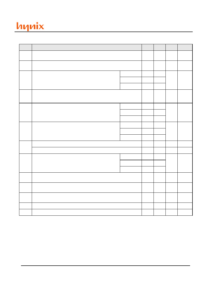
DC CHARACTERISTICS
(Vcc = 3.3V +/- 10%, TA=0 to 70
°
C
)
Note :
1. Icc depends on output load condition when the device is selected, Icc(max) is specified at the output open condition
2. Address can be changed once or less while /RAS=VIL
3. Address can be changed once or less while /CAS=VIH
4. /CAS = L (<=0.2) while /RAS=L (<=0.2)
5. L-Version
Symbol
Parameter
Min
Max
Unit
Note
VOH
Output Level
Output Level voltage(Iout= -2mA)
2.4
Vcc
V
VOL
Output Level
Output Level voltage(Iout=2mA)
0
0.4
V
ICC1
Operating current
Average power supply operating current
( /RAS, /CAS Cycling : tRC = tRC min)
50ns
-
100
mA
1, 2
60ns
-
90
70ns
-
80
I
CC2
Standby current (TTL interface)
Power supply standby current
(/RAS, /CAS=VIH, Dout = High-Z)
-
2
mA
ICC3
/RAS only refresh current
Average power supply current
/RAS only refresh mode
(tRC= tRC min)
50ns
-
100
mA
2
60ns
-
90
70ns
-
80
ICC4
Fast page mode current
Average power supply current
Fast page mode (tPC=tPC min)
50ns
-
90
mA
1, 3
60ns
-
80
70ns
-
75
ICC5
CMOS interface ( /RAS, /CAS >= Vcc-0.2V, Dout = High-Z)
-
1
mA
Standby current ( L-version)
-
100
uA
4
ICC6
/CAS-before-/RAS refresh current (tRC=tRC min)
50ns
-
100
mA
60ns
-
90
70ns
-
80
ICC7
Battery back up operating current (standby with CBR refresh)
(tRC=31.3us, tRAS<=0.3us, Dout=High-Z)
-
300
uA
4
ICC8
Standby current
( /RAS = VIH, /CAS = VIL, Dout=Enable)
-
5
uA
1
ICC9
Self refresh current
(/RAS, /CAS <=0.2V, Dout=High-Z, CMOS interface)
-
200
uA
4
II(L)
Input leakage current, Any input (0V<= Vin<=4.6V)
-10
10
uA
IO(L)
Output leakage current, (Dout is disabled, 0V<= Vout<=4.6V)
-10
10
uA
HY51V(S)17403HG/HGL
Rev.0.1/Apr.01
5
CAPACITANCE
(Vcc=3.3V +/-10%, TA=25
°
C
)
Note : 1. Capacitance measured with Boonton Meter or effective capacitance measuring method.
2. /CAS = V
IH
to disable D
out
AC CHARACTERISTICS
(Vcc=3.3V +/-10%, TA=0~70C, Note 1, 2, 18)
Read, Write, Read-modify-Write and Refresh Cycle
Parameter
Symbol
Min.
Max
Unit
Note
Input capacitance (Address)
CI1
-
5
pF
1
Input capacitance (Clocks)
CI2
-
7
pF
1
Output capacitance (Data-in, Data-out)
CI/O
-
7
pF
1, 2
Parameter
Symbol
-50
-60
-70
Unit
Note
Min
Max
Min
Max
Min
Max
Random read or write cycle time
t
RC
84
-
104
-
124
-
ns
/RAS precharge time
t
RP
30
-
40
-
50
-
ns
/CAS precharge time
t
CP
8
-
10
-
13
-
ns
/RAS pulse width
t
RAS
50
10,000
60
10,000
70
10,000
ns
/CAS pulse width
t
CAS
8
10,000
10
10,000
13
10,000
ns
Row address set-up time
t
ASR
0
-
0
-
0
-
ns
Row address hold time
t
RAH
8
-
10
-
10
-
ns
Column address set-up time
t
ASC
0
-
0
-
0
-
ns
Column address hold time
t
CAH
8
-
10
-
13
-
ns
/RAS to /CAS delay time
t
RCD
12
37
14
45
14
52
ns
3
/RAS to Column address delay time
t
RAD
10
25
12
30
12
35
ns
4
/RAS hold time
t
RSH
10
-
13
-
13
-
ns
/CAS hold time
t
CSH
35
-
40
-
45
-
ns
/CAS to /RAS precharge time
t
CRP
5
-
5
-
5
-
ns
Test Condition
·
Input rise and fall times = 2ns
·
Input levels : V
IL
=0V, V
IH
=3V
·
Input timing reference level : V
IL
/V
IH
= 0.8/2.0V
·
Output timing reference level :
V
OL
/V
OH
=0.8/0.2V
·
Output load : 1 TTL gate + C
L
(100pF)
( including scope and jig )
HY51V(S)17403HG/HGL
Rev.0.1/Apr.01
6
- continued -
Read Cycle
Parameter
Symbol
-50
-60
-70
Unit
Note
Min
Max
Min
Max
Min
Max
/OE to Din delay time
t
ODD
13
-
15
-
18
-
ns
5
/OE delay time from Din
t
DZO
0
-
0
-
0
-
ns
6
/CAS delay time from Din
tDZC
0
-
0
-
0
-
ns
6
Transition time ( Rise and Fall)
t
T
2
50
2
50
2
50
ns
7
Refresh period
t
REF
-
32
-
32
-
32
ms
2K Ref.
Refresh period (L-version)
-
128
-
128
-
128
ms
2K Ref.
Parameter
Symbol
-50
-60
-70
Unit
Note
Min
Max
Min
Max
Min
Max
Access time from /RAS
t
RAC
-
50
-
60
-
70
ns
8,9,19
Access time from /CAS
t
CAC
-
13
-
15
-
18
ns
9,10,
17,19
Access time from column address
tAA
-
25
-
30
-
35
ns
9,11,
17,19
Access time from /OE
t
OAC
-
13
-
15
-
18
ns
9
Read command set-up time
t
RCS
0
-
0
-
0
-
ns
Read command hold time to /CAS
tRCH
0
-
0
-
0
-
ns
12
Read command hold time from /RAS
t
RCHR
50
-
60
-
70
-
ns
Read command hold time to /RAS
t
RRH
5
-
5
-
5
-
ns
12
Column address to /RAS lead time
t
RAL
25
-
30
-
35
-
ns
Column address to /CAS lead time
tCAL
15
-
18
-
23
-
ns
/CAS to output in low-Z
tCLZ
0
-
0
-
0
-
ns
Output data hold time
t
OH
3
-
3
-
3
-
ns
Output data hold time from /OE
tOHO
3
-
3
-
3
-
ns
Output buffer turn off time to /OE
t
OEZ
-
13
-
15
-
15
ns
13
Output buffer turn off time
t
OFF
-
13
-
15
-
15
ns
13
/CAS to Din delay time
tCDD
13
-
15
-
18
-
ns
5
Output data hold time from /RAS
t
OHR
3
-
3
-
3
-
ns
Output buffer turn-off time to /RAS
tOFR
-
13
-
15
-
15
ns
Output buffer turn off time to /WE
t
WEZ
-
13
-
15
-
15
ns
/WE to DIN delay time
t
WDD
13
-
15
-
18
-
ns
/RAS to DIN delay time
tRDD
13
-
15
-
18
-
ns
HY51V(S)17403HG/HGL
Rev.0.1/Apr.01
7
Write Cycle
Read-Modify-Write Cycle
Refresh cycle
Parameter
Symbol
-50
-60
-70
Unit
Note
Min
Max
Min
Max
Min
Max
Write command set-up time
tWCS
0
-
0
-
0
-
ns
14
Write command hold time
t
WCH
8
-
10
-
13
-
ns
Write command pulse width
tWP
8
-
10
-
10
-
ns
Write command to /RAS lead time
t
RWL
8
-
10
-
13
-
ns
Write command to /CAS lead time
t
CWL
8
-
10
-
13
-
ns
Data-in set-up time
tDS
0
-
0
-
0
-
ns
15
Data-in hold time
tDH
8
-
10
-
13
-
ns
15
Parameter
Symbol
-50
-60
-70
Unit
Note
Min
Max
Min
Max
Min
Max
Read-modify-write cycle time
tRWC
111
-
136
-
161
-
ns
/RAS to /WE delay time
t
RWD
67
-
79
-
92
-
ns
14
/CAS to /WE delay time
tCWD
30
-
34
-
40
-
ns
14
Column address to /WE delay time
t
AWD
42
-
49
-
57
-
ns
14
/OE hold time from /WE
t
OEH
13
-
15
-
18
-
ns
Parameter
Symbol
-50
-60
-70
Unit
Note
Min
Max
Min
Max
Min
Max
/CAS set-up time
( /CAS-before-/RAS Refresh Cycle)
tCSR
5
-
5
-
5
-
ns
/CAS hold time
( /CAS-before-/RAS Refresh Cycle)
t
CHR
8
-
10
-
10
-
ns
/WE setup time
( /CAS-before-/RAS Refresh Cycle)
t
WRP
0
-
0
-
0
-
ns
/WE hold time
( /CAS-before-/RAS Refresh Cycle)
t
WRH
10
-
10
-
10
-
ns
/RAS precharge to /CAS hold time
( /CAS-before-/RAS Refresh Cycle)
t
RPC
5
-
5
-
5
-
ns
HY51V(S)17403HG/HGL
Rev.0.1/Apr.01
8
EDO Page Mode Cycle
EDO Page Mode Read-Modify-Write Cycle
TEST Mode cycle
Self Refresh Mode(L-version)
Parameter
Symbol
-50
-60
-70
Unit
Note
Min
Max
Min
Max
Min
Max
EDO mode cyle time
tHPC
20
-
25
-
30
-
ns
20
EDO mode /RAS pulse width
tRASP
-
100K
-
100K
-
100K
ns
16
Access time from /CAS precharge
tACP
-
30
-
35
-
40
ns
9,17,19
/RAS hold time from /CAS precharge
tRHCP
30
-
35
-
40
-
ns
Output data hold time from /CAS low
tDOH
3
-
3
-
3
-
ns
9
/CAS hold time referred /OE
tCOL
8
-
10
-
13
-
ns
/CAS to /OE setup time
tCOP
5
-
5
-
5
-
ns
Read command hold time
from /CAS precharge
tRHCP
30
-
35
-
40
-
ns
Parameter
Symbol
-50
-60
-70
Unit
Note
Min
Max
Min
Max
Min
Max
EDO Page read-modify-write cycle time
tHPRWC
57
-
68
-
79
-
ns
EDO mode read-modify-write cycle
/CAS precharge to /WE delay time
tCPW
45
-
54
-
62
-
ns
14
Parameter
Symbol
-50
-60
-70
Unit
Note
Min
Max
Min
Max
Min
Max
Test mode /WE setup time
tWTS
0
-
0
-
0
-
ns
Test mode /WE hold time
tWTH
10
-
10
-
10
-
ns
Parameter
Symbol
-50
-60
-70
Unit
Note
Min
Max
Min
Max
Min
Max
/RAS pulse width (self refresh)
tRASS
100
-
100
-
100
-
us
/RAS precharge time(self refresh)
tRPS
90
-
110
-
130
-
ns
/CAS hold time(self refresh)
tCHS
-50
-
-50
-
-50
-
ns

HY51V(S)17403HG/HGL
Rev.0.1/Apr.01
9
Notes :
1. AC measurements assume t
T
= 2ns
2. AC initial pause of 200us is required after power up followed by a minimum of eight initialization cycles
( any combination of cycles containing /RAS-only refresh or /CAS-before-/RAS refresh)
If the internal refresh counter is used, a minimum of eight /CAS-before-/RAS refresh cycle are required.
3. Operation with the t
RCD
(max) limit insures that t
RAC
(max) can be met, t
RCD
(max) is specified as a
reference point only : if t
RCD
is greater than the specified t
RCD
(max) limit, then access time is
controlled exclusively by t
CAC
.
4. Operation with the t
RAD
(max) limit insures that t
RAC
(max) can be met, t
RAD
(max) is specified as a
reference point only : if t
RAD
is greater than the specified t
RAD
(max) limit, then access time is
controlled exclusively by t
AA
.
5. Either t
ODD
or t
CDD
must be satisfied.
6. Either t
DZO
or t
DZC
must be satisfied.
7. V
IH
(min) and V
IL
(max) are reference levels for measuring timing of input signals, also transition times
are measured between V
IH
(min) and V
IL
(max)
8. Assumes that t
RCD
<=t
RCD
(max) and t
RAD
<=t
RAD
(max). If t
RCD
or t
RAD
is greater than the maximum
recommended value shown in this table, t
RAC
exceeds the value shown
9. Measured with a load circuit equivalent to 1 TTL loads and 100pF.( V
OH
=2.0V, V
OL
=0.8V)
10. Assumes that t
RCD
>=t
RCD
(max) and t
RCD
+ t
CAC
(max) >= t
RAD
+ t
AA
(max)
11. Assumes that t
RAD
>=t
RAD
(max) and t
RCD
+ t
CAC
(max) <= t
RAD
+ t
AA
(max)
12. Either t
RCH
of t
RRH
must be satified for a read cycles
13. t
OFF
(max), t
OEZ
(max), t
OFR
(max) and t
WEZ
(max) define the time at which the outputs achieve the
open circuit condition and is not referenced to output voltage levels
14. t
WCS
, t
RWD
, t
CWD
, t
AWD
and t
CPW
are not restrictive operating parameters. They are included in
the data sheet as electrical characteristics only : If t
WCS
>=t
WCS
(min), the cycle is an early write
cycle and the data out pin will remain open circuit(high impedance) throughout the entire cycle :
If t
RWD
>=t
RWD
(min), t
CWD
>=t
CWD
(min), t
AWD
>=t
AWD
(min), the cycle is a read-modify-write and
the data output will contain data read from the selected cell : if neither of the above sets of conditions
is satified, the condition of the data out (at access time) is indeterminate.
15. These parameters are referenced to /CAS leading edge in early write cycles and to /WE
leading edge in delayed write or read-modify-write cycles
16. t
RASP
defines /RAS pulse width in EDO p
age mode cycles

HY51V(S)17403HG/HGL
Rev.0.1/Apr.01
10
17. Access time is determined by the longest among t
AA
or t
CAC
or t
ACP
18. The 16M DRAM offers 16 bit time saving parallel test mode. Address CA0 and CA1 for the 4Mx4 are
don't care during test mode. Test mode is set by performing a /WE-and-/CAS-before-/RAS(WCBR)
cycle. In 16bit parallel test mode, data is written into 4 bits in parallel at each I/O(I/O 1 to I/O4) and
read out from each I/O. If 4 bits of each I/O are equal (all 1s or 0s), data output pin is a high state
during test mode read cycle, then the device has passed. If they are not equal, Data output pin is a
low state, then the device has failed. Refresh during test mode operation can be performed by normal
read cycles or by WCBR refresh cycles. To get out of test mode and enter a normal operation mode,
perform either a regular /CAS-before-/RAS refresh cycle or /RAS-only refresh cycle.
19. In a test mode read cycle, the value of t
RAC
, t
AA
, t
CAC
and t
ACP
is delayed by 2ns to 5ns for the
specified value. These parameters should be specified in test mode cycles by adding the above value
to the specified value in this data sheet
20. t
HPC
(min) can be achieved during a series of EDO page mode write cycles or EDO page mode read
cycles. If both write and read operation are mixed in a EDO page mode /RAS cycle(EDO page mode
mix cycle (1)(2)), minimum value of /CAS cycle(t
CAS
+t
CP
+2t
T
) becomes greater than the specified
t
HPC
(min) value. The value of /CAS cycle time of mixed EDO page mode is shown in EDO page mode
mix cycle (1) and (2)
HY51V(S)17403HG/HGL
Rev.0.1/Apr.01
11
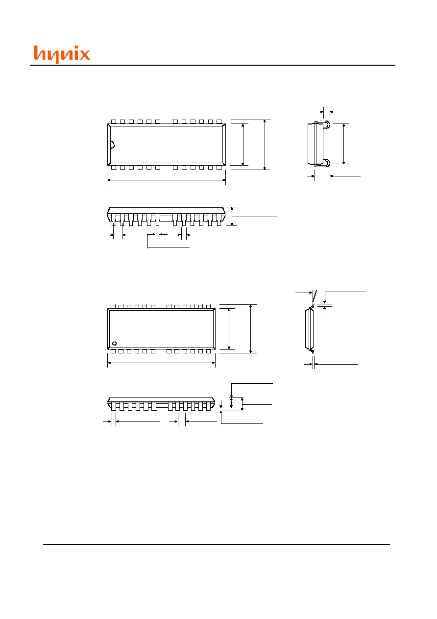
PACKAGE INFORMATION
Unit: Inches (mm)
24(26)pin TSOP-II
24(26)pin SOJ
0.669(17.00) MAX
0.661(16.80) MIN
0.295(7.49)
MIN
0.329(8.38)
MIN
0.340(8.64)
MAX
0.147(3.75) MAX
0.128(3.25) MIN
0.020(0.50) MAX
0.015(0.38) MIN
TYP
0.050(1.27)
0.305(7.75)
MAX
0.260(6.60)
MIN
0.275(6.99)
MAX
0.025(0.64)
MIN
0.032(0.81) MAX
0.026(0.66) MIN
0.085(2.16)
MIN
0.020(0.50) MAX
0.012(0.30) MIN
TYP
0.050(1.27)
0.007(0.18) MAX
0.003(0.08) MIN
0.047(1.20)
MAX
0.041(1.05) MAX
0.037(0.95) MIN
0.296(7.52)
MIN
0.303(7.72)
MAX
0.678(17.24) MAX
0.670(17.04) MIN
0.355(9.02)
MIN
0.371(9.42)
MAX
0.024(0.60) MAX
0.016(0.40) MIN
0.008(0.21) MAX
0.004(0.12) MIN
0 ~ 5 Deg