This document is a general product description and is subject to change without notice. Hynix does not assume any responsibility for
use of circuits described. No patent licenses are implied.
Rev 0.6 / Oct. 2004
1
HY27SS(08/16)121M Series
HY27US(08/16)121M Series
512Mbit (64Mx8bit / 32Mx16bit) NAND Flash
Document Title
512Mbit (64Mx8bit / 32Mx16bit) NAND Flash Memory
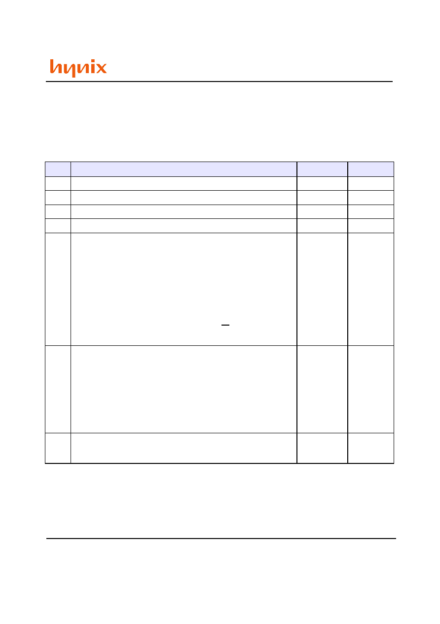
Revision History
No.
History
Draft Date
Remark
0.0
Initial Draft
Sep.17.2003
Preliminary
0.1
Renewal Product Group
Oct.07.2003
Preliminary
0.2
Make a decision of PKG information
Nov.08.2003
Preliminary
0.3
Append 1.8V Operation Product to Data sheet
Dec.01.2003
Preliminary
0.4
1) Add Errata
2) Modify the description of Device Operations
- /CE Don't Care Enabled(Disabled) -> Sequential Row Read Disabled
(Enabled) (Page22)
3) Add the description of System Interface Using CE don't care
(Page37)
Mar.28.2004
Preliminary
0.5
1) Delete Errata
2) Change Characteristics (3V Product)
3) Delete Cache Program
Jun. 01. 2004
Preliminary
0.6
1) Change TSOP1, WSOP1, FBGA package dimension
2) Edit TSOP1, WSOP1 package figures
3) Change FBGA package figure
Oct. 20. 2004
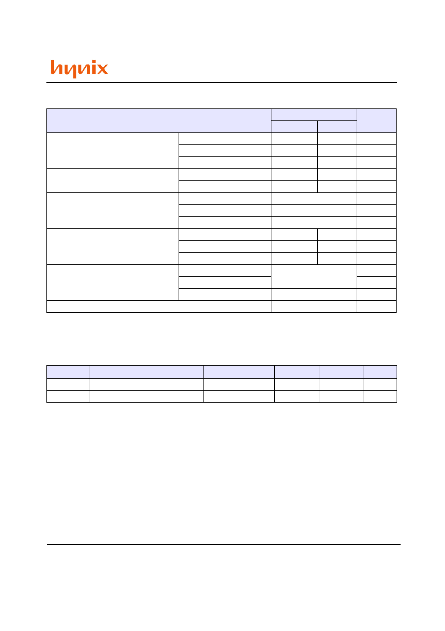
tCRY
tREA@ID Read
Before
60 + tr
35
After
70 + tr
45
tWC
tWH
tWP
tRC
tREH
tRP
tREA@ID Read
Specification
50
15
25
50
15
30
35
Relaxed value
60
20
40
60
20
40
45

This document is a general product description and is subject to change without notice. Hynix does not assume any responsibility for
use of circuits described. No patent licenses are implied.
Rev 0.6 / Oct. 2004
2
HY27SS(08/16)121M Series
HY27US(08/16)121M Series
512Mbit (64Mx8bit / 32Mx16bit) NAND Flash
FEATURES SUMMARY
HIGH DENSITY NAND FLASH MEMORIES
- Cost effective solutions for mass storage applications
NAND INTERFACE
- x8 or x16 bus width.
- Multiplexed Address/ Data
- Pinout compatibility for all densities
SUPPLY VOLTAGE
- 3.3V device: VCC = 2.7 to 3.6V : HY27USXX121M
- 1.8V device: VCC = 1.7 to 1.95V : HY27SSXX121M
Memory Cell Array
- 528Mbit = 528 Bytes x 32 Pages x 4,096 Blocks
PAGE SIZE
- x8 device : (512 + 16 spare) Bytes
: HY27(U/S)S08121M
- x16 device: (256 + 8 spare) Words
: HY27(U/S)S16121M
BLOCK SIZE
- x8 device: (16K + 512 spare) Bytes
- x16 device: (8K + 256 spare) Words
PAGE READ / PROGRAM
- Random access: 12us (max)
- Sequential access: 50ns (min)
- Page program time: 200us (typ)
COPY BACK PROGRAM MODE
- Fast page copy without external buffering
FAST BLOCK ERASE
- Block erase time: 2ms (Typ)
STATUS REGISTER
ELECTRONIC SIGNATURE
Sequential Row Read OPTION
AUTOMATIC PAGE 0 READ AT POWER-UP
OPTION
- Boot from NAND support
- Automatic Memory Download
SERIAL NUMBER OPTION
HARDWARE DATA PROTECTION
- Program/Erase locked during Power transitions
DATA INTEGRITY
- 100,000 Program/Erase cycles
- 10 years Data Retention
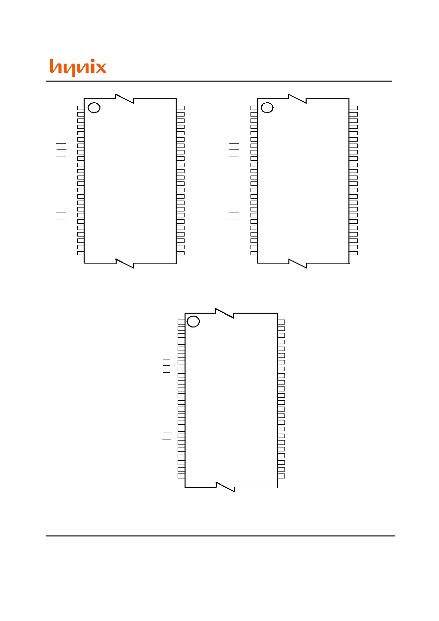
PACKAGE
- HY27US(08/16)121M-T(P)
: 48-Pin TSOP1 (12 x 20 x 1.2 mm)
- HY27US(08/16)121M-T (Lead)
- HY27US(08/16)121M-TP (Lead Free)
- HY27US08121M-V(P)
: 48-Pin WSOP1 (12 x 17 x 0.7 mm)
- HY27US08121M-V (Lead)
- HY27US08121M-VP (Lead Free)
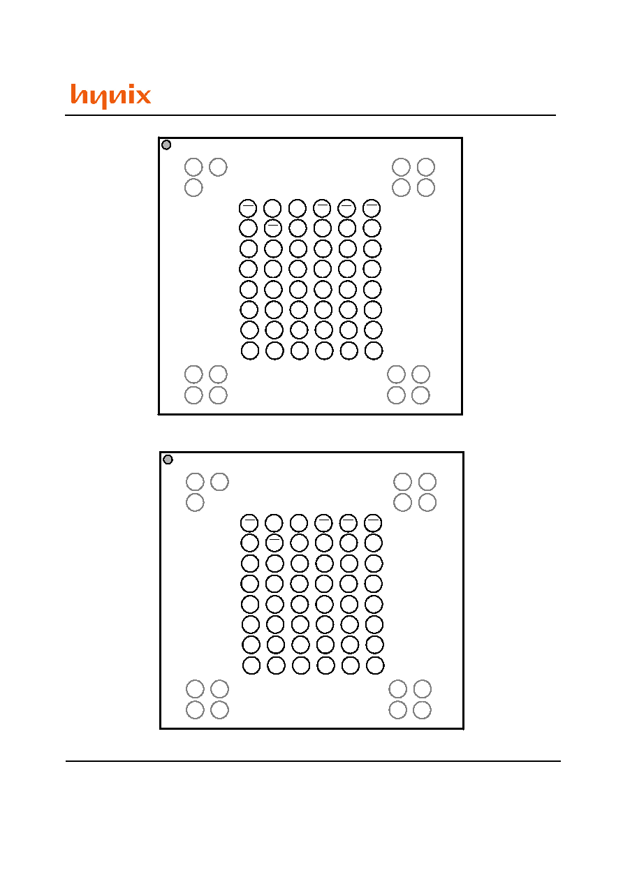
- HY27(U/S)S(08/16)121M-F(P)
: 63-Ball FBGA (8.5 x 15 x 1.2 mm)
- HY27US(08/16)121M-F (Lead)
- HY27US(08/16)121M-FP (Lead Free)
- HY27SS(08/16)121M-F (Lead)
- HY27SS(08/16)121M-FP (Lead Free)

Rev 0.6 / Oct. 2004
3
HY27SS(08/16)121M Series
HY27US(08/16)121M Series
512Mbit (64Mx8bit / 32Mx16bit) NAND Flash
DESCRIPTION
The HYNIX HY27(U/S)SXX121M series is a family of non-volatile Flash memories that use NAND cell technology. The
devices operate 3.3V and 1.8V voltage supply. The size of a Page is either 528 Bytes (512 + 16 spare) or 264 Words
(256 + 8 spare) depending on whether the device has a x8 or x16 bus width.
The address lines are multiplexed with the Data Input/ Output signals on a multiplexed x8 or x16 Input/ Output bus.
This interface reduces the pin count and makes it possible to migrate to other densities without changing the footprint.
Each block can be programmed and erased over 100,000 cycles. To extend the lifetime of NAND Flash devices it is
strongly recommended to implement an Error Correction Code (ECC). A Write Protect pin is available to give a hard-
ware protection against program and erase operations.
The devices feature an open-drain Ready/Busy output that can be used to identify if the Program/ Erase/Read (PER)
Controller is currently active. The use of an open-drain output allows the Ready/ Busy pins from several memories to
be connected to a single pull-up resistor.
A Copy Back command is available to optimize the management of defective blocks. When a Page Program operation
fails, the data can be programmed in another page without having to resend the data to be programmed.
The devices are available in the following packages:
- 48-TSOP1 (12 x 20 x 1.2 mm)
- 48-WSOP1 (12 x 17 x 0.7 mm)
- 63-FBGA (8.5 x 15 x 1.2 mm, 6 x 8 ball array, 0.8mm pitch)
Three options are available for the NAND Flash family:
- Automatic Page 0 Read after Power-up, which allows the microcontroller to directly download the boot code from
page 0.
- Chip Enable Dont Care, which allows code to be directly downloaded by a microcontroller, as Chip Enable transitions
during the latency time do not stop the read operation.
- A Serial Number, which allows each device to be uniquely identified. The Serial Number options is subject to an NDA
(Non Disclosure Agreement) and so not described in the datasheet. For more details of this option contact your near-
est HYNIX Sales office.
Devices are shipped from the factory with Block 0 always valid and the memory content bits, in valid blocks, erased to
'1'.
Rev 0.6 / Oct. 2004
4
HY27SS(08/16)121M Series
HY27US(08/16)121M Series
512Mbit (64Mx8bit / 32Mx16bit) NAND Flash
I/O
8-15
Data Input/Outputs for x16 Device
I/O
0-7
Data Input/Output, Address Inputs, or Com-
mand Inputs for x8 and x16 device
ALE
Address Latch Enable
CLE
Command Latch Enable
CE
Chip Enable
RE
Read Enable
RB
Read/Busy (open-drain output)
WE
Write Enable
WP
Write Protect
VCC
Supply Voltage
VSS
Ground
NC
Not Connected Internally
DU
Do Not Use
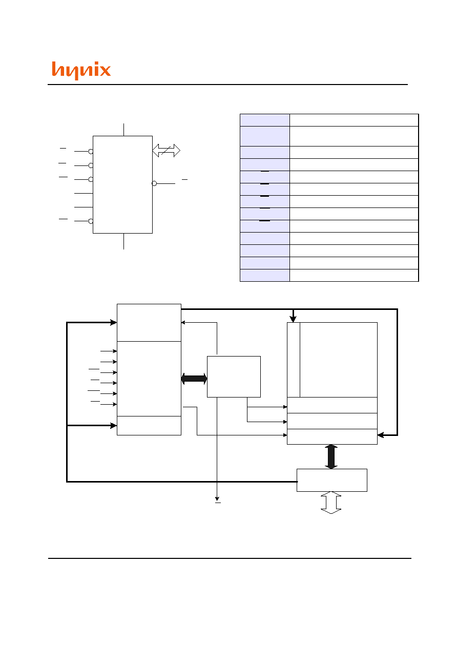
Table 1: Signal Name
Figure 1: Logic Diagram
Figure 2. LOGIC BLOCK DIAGRAM
NAND
Flash
Vcc
Vss
ALE
CLE
CE
RE
WE
WP
I/O8-I/O15, x16
I/O0-I/O7, x8/x16
RB
I/O Buffers &
Latches
Page Buffer
Cache Register
Y Decoder
NAND Flash
Memory Array
Address
Register/Counter
Command
Interface
Logic
Command Register
P/E/R
Controller,
High Voltage
Generator
X De
co
de
r
ALE
CLE
WE
CE
WP
RE
I/O0-I/O7, x8/x16
I/O8-I/O15, x16
RB
Rev 0.6 / Oct. 2004
5
HY27SS(08/16)121M Series
HY27US(08/16)121M Series
512Mbit (64Mx8bit / 32Mx16bit) NAND Flash
1
12
13
24
48
37
36
25
NC
NC
NC
NC
I/O7
I/O6
I/O5
I/O4
NC
NC
NC
Vcc
Vss
NC
NC
NC
I/O3
I/O2
I/O1
I/O0
NC
NC
NC
NC
NC
NC
NC
NC
NC
NC
CE
NC
NC
Vcc
Vss
NC
NC
CLE
ALE
NC
NC
NC
NC
NC
RB
RE
W E
W P
NAND Flash
(x8)
1
12
13
24
48
37
36
25
Vss
I/O15
I/O7
I/O14
I/O6
I/O13
I/O5
I/O12
I/O4
NC
NC
Vcc
NC
NC
NC
I/O11
I/O3
I/O10
I/O2
I/O9
I/O1
I/O8
I/O0
Vss
NC
NC
NC
NC
NC
NC
CE
NC
NC
Vcc
Vss
NC
NC
CLE
ALE
NC
NC
NC
NC
NC
RB
RE
W E
W P
NAND Flash
(x16)
1
12
13
24
48
37
36
25
NC
NC
NC
NC
I/O7
I/O6
I/O5
I/O4
NC
NC
NC
Vcc
Vss
NC
NC
NC
I/O3
I/O2
I/O1
I/O0
NC
NC
NC
NC
NC
NC
NC
NC
NC
NC
CE
NC
NC
Vcc
Vss
NC
NC
CLE
ALE
NC
NC
NC
NC
NC
RB
RE
W E
W P
NAND Flash
(x8)
1
12
13
24
48
37
36
25
NC
NC
NC
NC
I/O7
I/O6
I/O5
I/O4
NC
NC
NC
Vcc
Vss
NC
NC
NC
I/O3
I/O2
I/O1
I/O0
NC
NC
NC
NC
NC
NC
NC
NC
NC
NC
CE
NC
NC
Vcc
Vss
NC
NC
CLE
ALE
NC
NC
NC
NC
NC
RB
RB
RE
RE
W E
W E
W P
W P
NAND Flash
(x8)
1
12
13
24
48
37
36
25
Vss
I/O15
I/O7
I/O14
I/O6
I/O13
I/O5
I/O12
I/O4
NC
NC
Vcc
NC
NC
NC
I/O11
I/O3
I/O10
I/O2
I/O9
I/O1
I/O8
I/O0
Vss
NC
NC
NC
NC
NC
NC
CE
NC
NC
Vcc
Vss
NC
NC
CLE
ALE
NC
NC
NC
NC
NC
RB
RE
W E
W P
NAND Flash
(x16)
1
12
13
24
48
37
36
25
Vss
I/O15
I/O7
I/O14
I/O6
I/O13
I/O5
I/O12
I/O4
NC
NC
Vcc
NC
NC
NC
I/O11
I/O3
I/O10
I/O2
I/O9
I/O1
I/O8
I/O0
Vss
NC
NC
NC
NC
NC
NC
CE
NC
NC
Vcc
Vss
NC
NC
CLE
ALE
NC
NC
NC
NC
NC
RB
RB
RE
RE
W E
W E
W P
W P
NAND Flash
(x16)
Figure 3. 48-TSOP1 Contactions, x8 and x16 Device
Figure 4. 48-WSOP1 Contactions, x8 Device
12
13
24
NAND Flash
WSOP1
(x8)
37
36
25
NC
NC
DU
NC
I/O7
I/O6
I/O5
I/O4
NC
DU
NC
Vcc
Vss
NC
DU
NC
I/O3
I/O2
I/O1
I/O0
NC
DU
NC
NC
NC
NC
DU
NC
NC
NC
RB
RE
CE
DU
NC
Vcc
Vss
NC
DU
CLE
ALE
WE
WP
NC
NC
DU
NC
NC
1
48
12
13
24
NAND Flash
WSOP1
(x8)
37
36
25
NC
NC
DU
NC
I/O7
I/O6
I/O5
I/O4
NC
DU
NC
Vcc
Vss
NC
DU
NC
I/O3
I/O2
I/O1
I/O0
NC
DU
NC
NC
NC
NC
DU
NC
NC
NC
RB
RE
CE
DU
NC
Vcc
Vss
NC
DU
CLE
ALE
WE
WP
NC
NC
DU
NC
NC
1
48
Rev 0.6 / Oct. 2004
6
HY27SS(08/16)121M Series
HY27US(08/16)121M Series
512Mbit (64Mx8bit / 32Mx16bit) NAND Flash
Figure 5. 63-FBGA Contactions, x8 Device (Top view through package)
Figure 6. 63-FBGA Contactions, x16 Device (Top view through package)
6
5
4
3
2
1
A
B
C
D
E
F
G
H
ALE
VSS
CE
WE
RB
NC
RE
CLE
NC
NC
NC
NC
NC
NC
NC
NC
NC
WP
NC
NC
NC
NC
NC
NC
NC
NC
NC
NC
NC
NC
NC
I/O0
NC
NC
NC
VCC
NC
I/O1
NC
VCC
I/O5
I/O7
VSS
I/O2
I/O3
I/O4
I/O6
VSS
NC
NC
NC
NC
NC
NC
NC
NC
NC
NC
NC
NC
NC
NC
NC
10
9
8
7
J
K
L
M
4
6
5
4
3
2
1
A
B
C
D
E
F
G
H
ALE
VSS
CE
WE
RB
NC
RE
CLE
NC
NC
NC
NC
NC
NC
NC
NC
NC
WP
NC
NC
NC
NC
NC
NC
NC
NC
NC
I/O5
NC
I/O1
VCC
VCC
I/O6
I/O15
VSS
I/O2
I/O11
I/O4
I/O13
VSS
NC
NC
NC
NC
NC
NC
NC
NC
NC
NC
NC
NC
NC
NC
NC
10
9
8
7
J
K
L
M
4
I/O7
I/O8
I/O10
I/O12 I/O14
I/O0
I/O9
I/O3
Rev 0.6 / Oct. 2004
7
HY27SS(08/16)121M Series
HY27US(08/16)121M Series
512Mbit (64Mx8bit / 32Mx16bit) NAND Flash
MEMORY ARRAY ORGANIZATION
The memory array is made up of NAND structures where 16 cells are connected in series.
The memory array is organized in blocks where each block contains 32 pages. The array is split into two areas, the
main area and the spare area. The main area of the array is used to store data whereas the spare area is typically used
to store Error Correction Codes, software flags or Bad Block identification.
In x8 devices the pages are split into a main area with two half pages of 256 Bytes each and a spare area of 16 Bytes.
In the x16 devices the pages are split into a 256 Word main area and an 8 Word spare area. Refer to Figure 8, Memory
Array Organization.
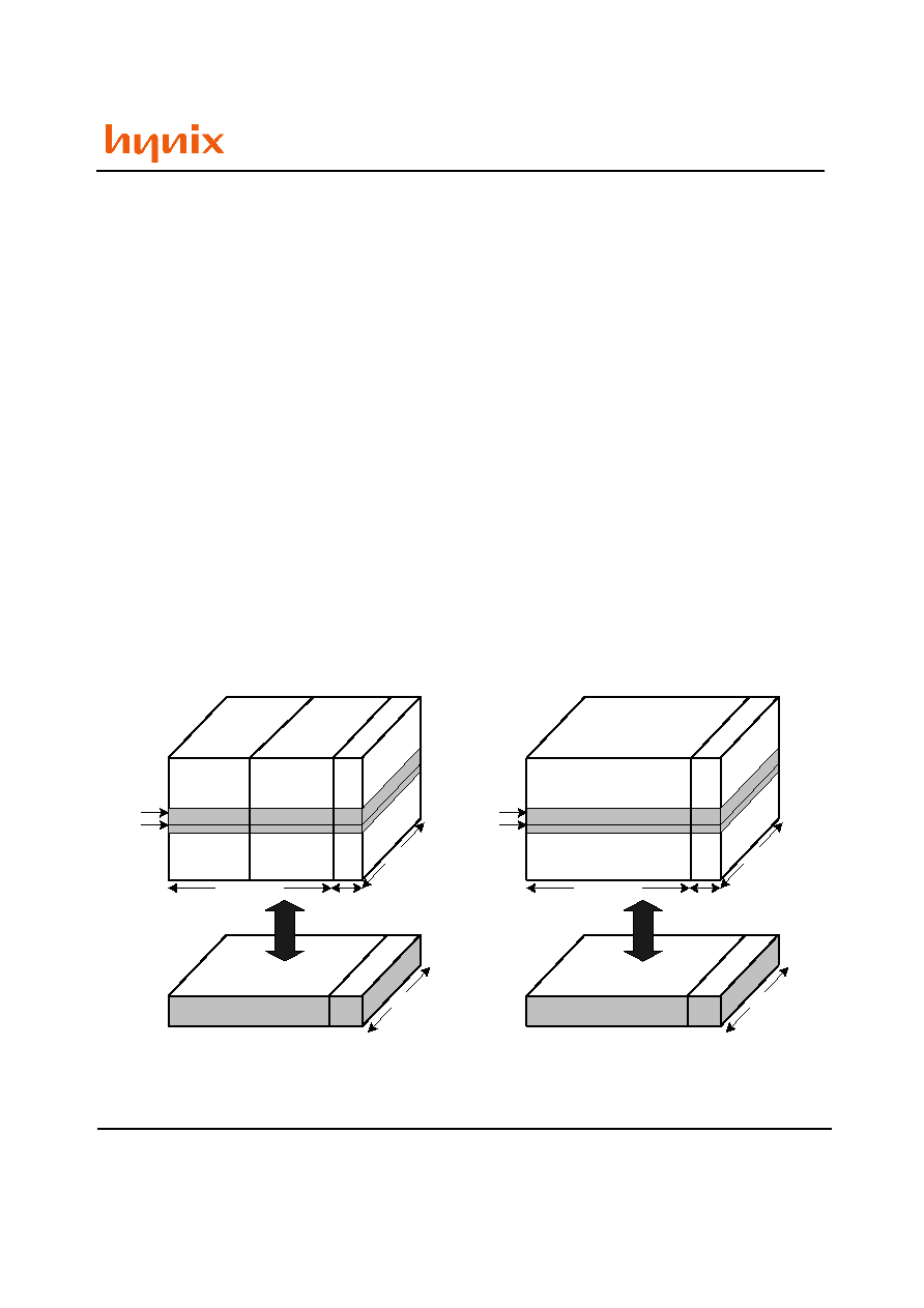
Bad Blocks
The NAND Flash 528 Byte/ 264 Word Page devices may contain Bad Blocks, that is blocks that contain one or more
invalid bits whose reliability is not guaranteed. Additional Bad Blocks may develop during the lifetime of the device.
The Bad Block Information is written prior to shipping (refer to Bad Block Management section for more details).
The values shown include both the Bad Blocks that are present when the device is shipped and the Bad Blocks that
could develop later on.
These blocks need to be managed using Bad Blocks Management, Block Replacement or Error Correction Codes.
Figure 7. Memory Array Organization
1st half Page
(256 bytes)
2nd half Page
(256 bytes)
Block
Page
512 Bytes
16
Bytes
8 bits
8 bits
512 Bytes
16
Bytes
Page Buffer, 528 Bytes
x8 DEVICES
Block= 32 Pages
Page= 528 Bytes (512+16)
Main Area
Block
Page
256 Words
8
Words
16 bits
16 bits
256 Words
8
Words
Page Buffer, 264 Words
x16 DEVICES
Block= 32 Pages
Page= 264 Words (256+8)
Sp
are
Ar
ea

Rev 0.6 / Oct. 2004
8
HY27SS(08/16)121M Series
HY27US(08/16)121M Series
512Mbit (64Mx8bit / 32Mx16bit) NAND Flash
SIGNAL DESCRIPTIONS
See Figure 1, Logic Diagram and Table 1, Signal Names, for a brief overview of the signals connected to this device.
Inputs/Outputs (I/O
0
-I/O
7
)
Input/Outputs 0 to 7 are used to input the selected address, output the data during a Read opertion or input a com-
mand or data during a Write operation. The inputs are latched on the rising edge of Write Enable. I/O
0
-I/O
7
can be left
floating when the device is deselected or the outputs are disabled.
Inputs/Outputs (I/O
8
-I/O
15
)
Input/Outputs 8 to 15 are only available in x16 devices. They are used to output the data during a Read operation or
input data during a Write operation. Command and Address Inputs only require I/O
0
to I/O
7
.
The inputs are latched on the rising edge of Write Enable. I/O
8
-I/O
15
can be left floating when the device is deselected
or the outputs are disabled.
Address Latch Enable (ALE)
The Address Latch Enable activates the latching of the Address inputs in the Command Interface. When ALE is high,
the inputs are latched on the rising edge of Write Enable.
Command Latch Enable (CLE)
The Command Latch Enable activates the latching of the Command inputs in the Command Interface. When CLE is
high, the inputs are latched on the rising edge of Write Enable.
Chip Enable (CE)
The Chip Enable input activates the memory control logic, input buffers, decoders and sense amplifiers. When Chip En-
able is low, V
IL
, the device is selected. If Chip Enable goes high, V
IH
, while the device is busy, the device remains se-
lected and does not go into standby mode.
When the device is executing a Sequential Row Read operation, Chip Enable must be held low (from the second page
read onwards) during the time that the device is busy (t
BLBH1
). If Chip Enable goes high during t
BLBH1
the operation is
aborted.
Read Enable (RE)
The Read Enable, RE, controls the sequential data output during Read operations. Data is valid t
RLQV
after the falling
edge of RE. The falling edge of RE also increments the internal column address counter by one.
Write Enable (WE). The Write Enable input, WE, controls writing to the Command Interface, Input Address and Data
latches. Both addresses and data are latched on the rising edge of Write Enable.
During power-up and power-down a recovery time of 1us (min) is required before the Command Interface is ready to
accept a command. It is recommended to keep Write Enable high during the recovery time.
Write Protect (WP).
The Write Protect pin is an input that gives a hardware protection against unwanted program or erase operations.
When Write Protect is Low, V
IL
, the device does not accept any program or erase operations.
It is recommended to keep the Write Protect pin Low, V
IL
, during power-up and power-down.

Rev 0.6 / Oct. 2004
9
HY27SS(08/16)121M Series
HY27US(08/16)121M Series
512Mbit (64Mx8bit / 32Mx16bit) NAND Flash
Ready/Busy (RB)
The Ready/Busy output, RB, is an open-drain output that can be used to identify if the Program/ Erase/ Read (PER)
Controller is currently active.
When Ready/Busy is Low, V
OL
, a read, program or erase operation is in progress. When the operation completes
Ready/Busy goes High, V
OH
.
The use of an open-drain output allows the Ready/ Busy pins from several memories to be connected to a single pull-
up resistor. A Low will then indicate that one, or more, of the memories is busy.
Refer to the Ready/Busy Signal Electrical Characteristics section for details on how to calculate the value of the pull-up
resistor.
V
CC
Supply Voltage
V
CC
provides the power supply to the internal core of the memory device. It is the main power supply for all operations
(read,program and erase).
An internal voltage detector disables all functions whenever V
CC
is below 2.5V (for 3V devices) or 1.5V (for 1.8V
devices) to protect the device from any involuntary program/erase during power-transitions.
Each device in a system should have V
CC
decoupled with a 0.1uF capacitor. The PCB track widths should be sufficient
to carry the required program and erase currents
V
SS
Ground
Ground, V
SS
, is the reference for the power supply. It must be connected to the system ground.
BUS OPERATIONS
There are six standard bus operations that control the memory. Each of these is described in this section, see Tables 2,
Bus Operations, for a summary.
Command Input
Command Input bus operations are used to give commands to the memory. Command are accepted when Chip Enable
is Low, Command Latch Enable is High, Address Latch Enable is Low and Read Enable is High. They are latched on the
rising edge of the Write Enable signal.
Only I/O
0
to I/O
7
are used to input commands. See Figure 21 and Table 14 for details of the timings requirements.
Address Input
Address Input bus operations are used to input the memory address. Four bus cycles are required to input the
addresses for the 512Mb devices (refer to Tables 3 and 4, Address Insertion). The addresses are accepted when Chip
Enable is Low, Address Latch Enable is High, Command Latch Enable is Low and Read Enable is High. They are latched
on the rising edge of the Write Enable signal. Only I/O
0
to I/O
7
are used to input addresses.
See Figure 22 and Table 14 for details of the timings requirements.
Data Input
Data Input bus operations are used to input the data to be programmed.
Data is accepted only when Chip Enable is Low, Address Latch Enable is Low, Command Latch Enable is Low and Read
Enable is High. The data is latched on the rising edge of the Write Enable signal. The data is input sequentially using
the Write Enable signal.
See Figure 23 and Tables 14 and 15 for details of the timings requirements.

Rev 0.6 / Oct. 2004
10
HY27SS(08/16)121M Series
HY27US(08/16)121M Series
512Mbit (64Mx8bit / 32Mx16bit) NAND Flash
Data Output
Data Output bus operations are used to read: the data in the memory array, the Status Register, the Electronic Signa-
ture and the Serial Number. Data is output when Chip Enable is Low, Write Enable is High, Address Latch Enable is
Low, and Command Latch Enable is Low. The data is output sequentially using the Read Enable signal.
See Figure 24 and Table 15 for details of the timings requirements.
Write Protect
Write Protect bus operations are used to protect the memory against program or erase operations. When the Write
Protect signal is Low the device will not accept program or erase operations and so the contents of the memory array
cannot be altered. The Write Protect signal is not latched by Write Enable to ensure protection even during power-up.
Standby
When Chip Enable is High the memory enters Standby mode, the device is deselected, outputs are disabled and power
consumption is reduced.
Rev 0.6 / Oct. 2004
11
HY27SS(08/16)121M Series
HY27US(08/16)121M Series
512Mbit (64Mx8bit / 32Mx16bit) NAND Flash
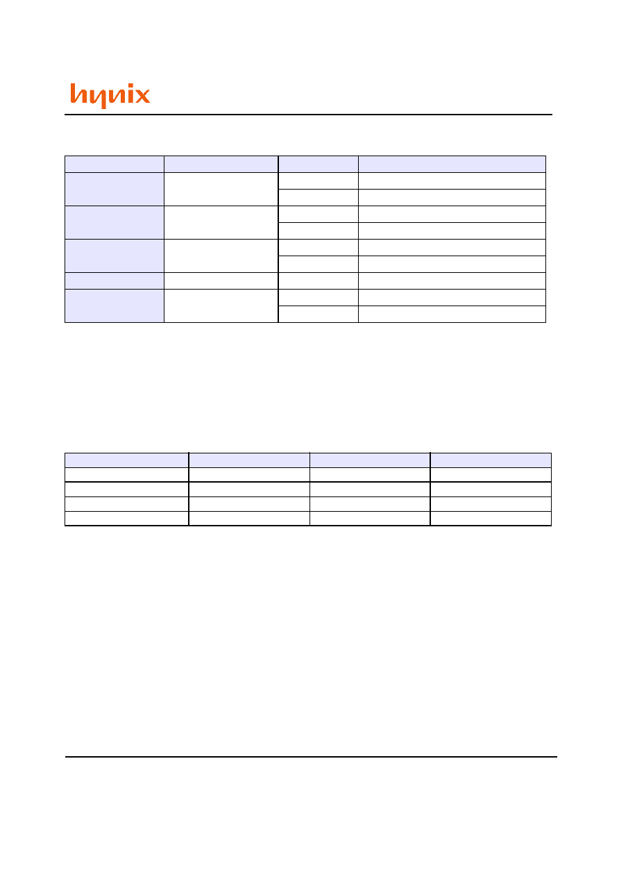
Table 2. Bus Operation
Note : (1) Only for x16 devices.
(2) WP must be V
IH
when issuing a program or erase command.
Table 3: Address Insertion, x8 Devices
Note: (1). A8 is set Low or High by the 00h or 01h Command, see Pointer Operations section.
(2). Any address input cycles will be ignored with tALS > 0ns.
Table4: Address Insertion, x16 Devices
Note: (1). A8 is Don
'
t Care in x16 devices.
(2). Any address input cycles will be ignored with tALS > 0ns.
(3). A1 is the Least Significant Address for x16 devices.
(4). The 01h Command is not used in x16 devices.
BUS Operation
CE
ALE
CLE
RE
WE
WP
I/O
0
- I/O
7
I/O
8
- I/O
15
(1)
Command Input
V
IL
V
IL
V
IH
V
IH
Rising
X
(2)
Command
X
Address Input
V
IL
V
IH
V
IL
V
IH
Rising
X
Address
X
Data Input
V
IL
V
IL
V
IL
V
IH
Rising
X
Data Input
Data Input
Data Output
V
IL
V
IL
V
IL
Falling
V
IH
X
Data Output
Data Output
Write Protect
X
X
X
X
X
V
IL
X
X
Standby
V
IH
X
X
X
X
X
X
X
Bus Cycle
I/O
7
I/O
6
I/O
5
I/O
4
I/O
3
I/O
2
I/O
1
I/O
0
1st Cycle
A7
A6
A5
A4
A3
A2
A1
A0
2nd Cycle
A16
A15
A14
A13
A12
A11
A10
A9
3rd Cycle
A24
A23
A22
A21
A20
A19
A18
A17
4th Cycle
V
IL
V
IL
V
IL
V
IL
V
IL
V
IL
V
IL
A25
Bus Cycle
I/O
8
-I/
O
15
I/O
7
I/O
6
I/O
5
I/O
4
I/O
3
I/O
2
I/O
1
I/O
0
1st Cycle
X
A7
A6
A5
A4
A3
A2
A1
A0
2nd Cycle
X
A16
A15
A14
A13
A12
A11
A10
A9
3rd Cycle
X
A24
A23
A22
A21
A20
A19
A18
A17
4th Cycle
V
IL
V
IL
V
IL
V
IL
V
IL
V
IL
V
IL
V
IL
A25

Rev 0.6 / Oct. 2004
12
HY27SS(08/16)121M Series
HY27US(08/16)121M Series
512Mbit (64Mx8bit / 32Mx16bit) NAND Flash
COMMAND SET
All bus write operations to the device are interpreted by the Command Interface. The Commands are input on I/O
0
-I/
O
7
and are latched on the rising edge of Write Enable when the Command Latch Enable signal is high. Device opera-
tions are selected by writing specific commands to the Command Register. The two-step command sequences for pro-
gram and erase operations are imposed to maximize data security.
The Commands are summarized in Table 5, Commands.
Table 5: Command Set
Note: (1). Any undefined command sequence will be ignored by the device.
(2). Bus Write Operation(1
st
, 2
nd
and 3
rd
Cycle) : The bus cycles are only shown for issuing the codes. The cycles required to
input the addresses or input/output data are not shown.
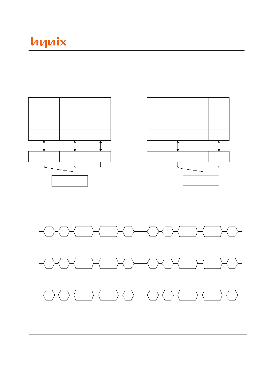
DEVICE OPERATIONS
Pointer Operations
As the NAND Flash memories contain two different areas for x16 devices and three different areas for x8 devices (see
Figure 8) the read command codes (00h, 01h, 50h) are used to act as pointers to the different areas of the memory
array (they select the most significant column address).
The Read A and Read B commands act as pointers to the main memory area. Their use depends on the bus width of
the device.
- In x16 devices the Read A command (00h) sets the pointer to Area A (the whole of the main area) that is Words 0
to 255.
- In x8 devices the Read A command (00h) sets the pointer to Area A (the first half of the main area) that is Bytes 0
to 255, and the Read B command (01h) sets the pointer to Area B (the second half of the main area) that is Bytes 256
to 511.
In both the x8 and x16 devices the Read C command (50h), acts as a pointer to Area C (the spare memory area) that
is Bytes 512 to 527 or Words 256 to 263.
Once the Read A and Read C commands have been issued the pointer remains in the respective areas until another
FUNCTION
1st CYCLE
2nd CYCLE
3rd CYCLE
Command accepted during busy
READ A
00h
-
-
READ B
01h
-
-
READ C
50h
-
-
READ ELECTRINIC SIGNATURE
90h
-
-
READ STATUS REGISTER
70h
-
-
Yes
PAGE PROGRAM
80h
10h
-
COPY BACK PROGRAM
00h
8Ah
10h
BLOCK ERASE
60h
D0h
-
RESET
FFh
-
-
Yes
Rev 0.6 / Oct. 2004
13
HY27SS(08/16)121M Series
HY27US(08/16)121M Series
512Mbit (64Mx8bit / 32Mx16bit) NAND Flash
pointer code is issued. However, the Read B command is effective for only one operation, once an operation has been
executed in Area B the pointer returns automatically to Area A.
The pointer operations can also be used before a program operation, that is the appropriate code (00h, 01h or 50h)
can be issued before the program command 80h is issued (see Figure 9).
Figure 8. Pointer Operation
Figure 9. Pointer Operations for Programming
Area A
(00h)
Area B
(01h)
Area C
(50h)
Bytes 0-255
Bytes 256-511
Bytes
512-527
A
B
C
Pointer
(00h, 01h, 50h)
x8 Devices
Page Buffer
Area C
(50h)
Words
256-263
C
x16 Devices
Page Buffer
Area A
(00h)
Words 0-256
A
Pointer
(00h, 50h)
10h
80h
01h
Address
Inputs
80h
Data
Input
10h
Address
Inputs
01h
Data
Input
AREA B
AREA B, C can be programmed depending on how much data is input.
The 01h command must be re-issued before each program.
10h
80h
00h
Address
Inputs
80h
Data
Input
10h
Address
Inputs
00h
Data
Input
AREA A
AREA A, B, C can be programmed depending on how much data is input.
Subsequent 00h commands can be omitted.
10h
80h
50h
Address
Inputs
80h
Data
Input
10h
Address
Inputs
50h
Data
Input
AREA C
Only Areas C can be programmed.
Subsequent 50h commands can be omitted.
I/O
I/O
I/O

Rev 0.6 / Oct. 2004
14
HY27SS(08/16)121M Series
HY27US(08/16)121M Series
512Mbit (64Mx8bit / 32Mx16bit) NAND Flash
Read Memory Array
Each operation to read the memory area starts with a pointer operation as shown in the Pointer Operations section.
The device defaults to Read A mode after powerup or a Reset operation. Devices, where page0 is read automatically at
power-up, are available on request.
When reading the spare area addresses:
- A0 to A3 (x8 devices)
- A0 to A2 (x16 devices)
are used to set the start address of the spare area while addresses:
- A4 to A7 (x8 devices)
- A3 to A7 (x16 devices)
are ignored.
Once the Read A or Read C commands have been issued they do not need to be reissued for subsequent read opera-
tions as the pointer remains in the respective area. However, the Read B command is effective for only one operation,
once an operation has been executed in Area B the pointer returns automatically to Area A and so another Read B
command is required to start another read operation in Area B.
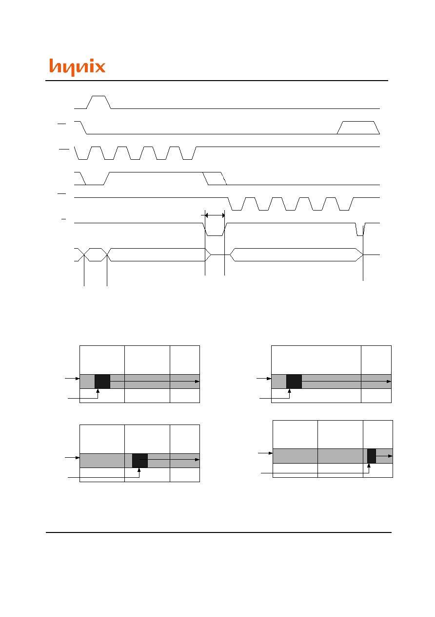
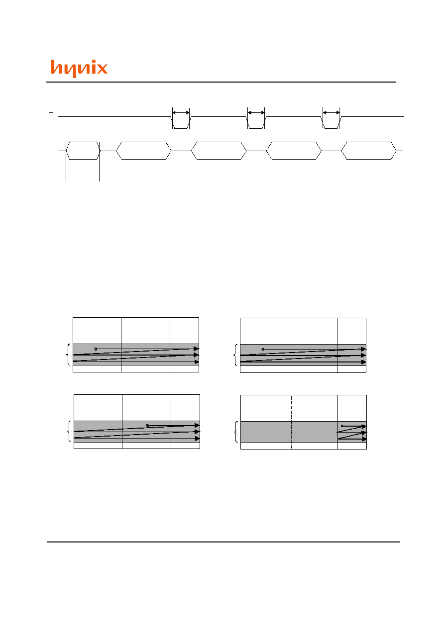
Once a read command is issued three types of operations are available: Random Read, Page Read and Sequential Row
Read.
Random Read
Each time the command is issued the first read is Random Read.
Page Read
After the Random Read access the page data is transferred to the Page Buffer in a time of t
WHBH
(refer to Table 15 for
value). Once the transfer is complete the Ready/Busy signal goes High. The data can then be read out sequentially
(from selected column address to last column address) by pulsing the Read Enable signal.
Sequential Row Read
After the data in last column of the page is output, if the Read Enable signal is pulsed and Chip Enable remains Low
then the next page is automatically loaded into the Page Buffer and the read operation continues. A Sequential Row
Read operation can only be used to read within a block. If the block changes a new read command must be issued.
Refer to Figures 12 and 13 for details of Sequential Row Read operations. To terminate a Sequential Row Read opera-
tion set the Chip Enable signal to High for more than t
EHEL
. Sequential Row Read is not available when the Sequential
row read option is disabled.
Rev 0.6 / Oct. 2004
15
HY27SS(08/16)121M Series
HY27US(08/16)121M Series
512Mbit (64Mx8bit / 32Mx16bit) NAND Flash
Note: 1. If t
ELWL
is less than 10ns, t
WLWH
must be minimum 35ns, otherwise, t
WLWH
may be minimum 25ns.
Note: 1. Highest address depends on device density.
Figure 10. Read (A, B, C) Operation
Figure 11. Read Block Diagrams
CLE
ALE
I/O
RB
tBLBH1
(read)
00h/
01h/ 50h
Command
Code
Address Input
Data Output (sequentially)
Busy
CE
WE
RE
Area A
(1st half Page)
Area B
(2nd half
Page)
Area C
(Spare)
Read A Command, x8 Devices
A9-A25(1)
A0-A7
Area C
(50h)
Read A Command, x16 Devices
Area A
(main area)
A9-A25(1)
A0-A7
Area A
Area C
(Spare)
Read C Command, x8/x16 Devices
A9-A25(1)
A0-A3 (x8)
A0-A2 (x16)
Area A/B
A4-A7 (x8), A3-A7 (x16) are don't care
Area A
(1st half Page)
Area C
(Spare)
Read B Command, x8 Devices
A9-A25(1)
A0-A7
Area B
(2nd half
Page)
Rev 0.6 / Oct. 2004
16
HY27SS(08/16)121M Series
HY27US(08/16)121M Series
512Mbit (64Mx8bit / 32Mx16bit) NAND Flash
Figure 12. Sequential Row Read Operation
Area A
(1
st
half Page)
Area B
Area C
Read A Command, x8 Devices
(2
nd
half Page) (Spare)
Block
1
st
Page
2
nd
Page
N
th
Page
Read B Command, x8 Devices
Area A
(1
st
half Page)
Area B
(2
nd
half Page)
Area C
(Spare)
Block
1
st
Page
2
nd
Page
N
th
Page
Area A
Area C
(Spare)
Read A Command, x16 Devices
(main area)
1
st
Page
2
nd
Page
N
th
Page
Block
Area A
Area A/B
Area C
(Spare)
Read C Command, x8/x16 Devices
1
st
Page
2
nd
Page
N
th
Page
Block
Area A
(1
st
half Page)
Area B
Area C
Read A Command, x8 Devices
(2
nd
half Page) (Spare)
Block
1
st
Page
2
nd
Page
N
th
Page
Area A
(1
st
half Page)
Area A
(1
st
half Page)
Area B
Area C
Read A Command, x8 Devices
(2
nd
half Page) (Spare)
Block
1
st
Page
2
nd
Page
N
th
Page
Block
1
st
Page
2
nd
Page
N
th
Page
Read B Command, x8 Devices
Area A
(1
st
half Page)
Area B
(2
nd
half Page)
Area C
(Spare)
Block
1
st
Page
2
nd
Page
N
th
Page
Read B Command, x8 Devices
Area A
(1
st
half Page)
Area A
(1
st
half Page)
Area B
(2
nd
half Page)
Area C
(Spare)
Block
1
st
Page
2
nd
Page
N
th
Page
Block
1
st
Page
2
nd
Page
N
th
Page
Area A
Area C
(Spare)
Read A Command, x16 Devices
(main area)
1
st
Page
2
nd
Page
N
th
Page
Block
Area A
Area C
(Spare)
Read A Command, x16 Devices
(main area)
1
st
Page
2
nd
Page
N
th
Page
Block
Block
Area A
Area A/B
Area C
(Spare)
Read C Command, x8/x16 Devices
1
st
Page
2
nd
Page
N
th
Page
Block
Area A
Area A/B
Area C
(Spare)
Read C Command, x8/x16 Devices
1
st
Page
2
nd
Page
N
th
Page
Block
1
st
Page
2
nd
Page
N
th
Page
Block
Figure 13. Sequential Row Read Block Diagrams
Busy
Busy
Busy
tBLBH1
(Read Busy time)
tBLBH1
tBLBH1
Address Inputs
I/O
00h/
01h/50h
1st
Page Output
2nd
Page Output
Nth
Page Output
Command
Code
RB
Rev 0.6 / Oct. 2004
17
HY27SS(08/16)121M Series
HY27US(08/16)121M Series
512Mbit (64Mx8bit / 32Mx16bit) NAND Flash
Page Program
The Page Program operation is the standard operation to program data to the memory array. The main area of the
memory array is programmed by page, however partial page programming is allowed where any number of bytes (1 to
528) or words (1 to 264) can be programmed.
The max number of consecutive partial page program operations allowed in the same page is one in the main area and
two in the spare area. After exceeding this a Block Erase command must be issued before any further program opera-
tions can take place in that page.
Before starting a Page Program operation a Pointer operation can be performed to point to the area to be pro-
grammed. Refer to the Pointer Operations section and Figure 9 for details.
Each Page Program operation consists of five steps (see Figure 14):
1. one bus cycle is required to setup the Page Program command
2. four bus cycles are then required to input the program address (refer to Table 3)
3. the data is then input (up to 528 Bytes/ 264 Words) and loaded into the Page Buffer
4. one bus cycle is required to issue the confirm command to start the Program/ Erase/Read Controller.
5. The Program/ Erase/Read Controller then programs the data into the array.
Once the program operation has started the Status Register can be read using the Read Status Register command.
During program operations the Status Register will only flag errors for bits set to '1' that have not been successfully
programmed to '0'.
During the program operation, only the Read Status Register and Reset commands will be accepted, all other com-
mands will be ignored.
Once the program operation has completed the Program/ Erase/Read Controller bit SR6 is set to '1' and the Ready/
Busy signal goes High.
The device remains in Read Status Register mode until another valid command is written to the Command Interface.
Note: Before starting a Page Program operation a Pointer operation can be performed. Refer to Pointer section for details.
Figure 14. Page Program Operation
Address Inputs
I/O
80h
Page Program
Setup Code
Data Input
10h
70h
SR0
Confirm
Code
Read Status Register
Busy
tBLBH2
(Program Busy time)
RB
Rev 0.6 / Oct. 2004
18
HY27SS(08/16)121M Series
HY27US(08/16)121M Series
512Mbit (64Mx8bit / 32Mx16bit) NAND Flash
Copy Back Program
The Copy Back Program operation is used to copy the data stored in one page and reprogram it in another page.
The Copy Back Program operation does not require external memory and so the operation is faster and more efficient
because the reading and loading cycles are not required. The operation is particularly useful when a portion of a block
is updated and the rest of the block needs to be copied to the newly assigned block.
If the Copy Back Program operation fails an error is signalled in the Status Register. However as the standard external
ECC cannot be used with the Copy Back operation bit error due to charge loss cannot be detected. For this reason it is
recommended to limit the number of Copy Back operations on the same data and/or to improve the performance of
the ECC.
The Copy Back Program operation requires three steps:
- 1. The source page must be read using the Read A command (one bus write cycle to setup the command and then
4 bus write cycles to input the source page address). This operation copies all 264 Words/ 528 Bytes from the page
into the Page Buffer.
- 2. When the device returns to the ready state (Ready/Busy High), the second bus write cycle of the command is
given with the 4 bus cycles to input the target page address.
A25
must be the same for the Source and Target Pages.
- 3. Then the confirm command is issued to start the P/E/R Controller.
After a Copy Back Program operation, a partial page program is not allowed in the target page until the block has been
erased.
See Figure 15 for an example of the Copy Back operation.
Block Erase
Erase operations are done one block at a time. An erase operation sets all of the bits in the addressed block to '1'. All
previous data in the block is lost. An erase operation consists of three steps (refer to Figure 17):
1. One bus cycle is required to setup the Block Erase command.
2. Only three bus cycles for 512Mb devices are required to input the block address. The first cycle (A0 to A7) is not
required as only addresses A14 to A25 (highest address depends on device density) are valid, A9 to A13 are ignored.
In the last address cycle I/O
0
to I/O
7
must be set to V
IL
.
3. One bus cycle is required to issue the confirm command to start the P/E/R Controller.
Figure 15. Copy Back Operation
Source
Address Inputs
I/O
00h
Copy Back
Code
Target
Address Inputs
8Ah
10h
70h
Read
Code
Read Status Register
SR0
Busy
tBLBH2
(Program Busy time)
tBLBH1
(Read Busy time)
RB

Rev 0.6 / Oct. 2004
19
HY27SS(08/16)121M Series
HY27US(08/16)121M Series
512Mbit (64Mx8bit / 32Mx16bit) NAND Flash
Once the erase operation has completed the Status Register can be checked for errors.
Reset
The Reset command is used to reset the Command Interface and Status Register. If the Reset command is issued dur-
ing any operation, the operation will be aborted. If it was a program or erase operation that was aborted, the contents
of the memory locations being modified will no longer be valid as the data will be partially programmed or erased.
If the device has already been reset then the new Reset command will not be accepted. The Ready/Busy signal goes
Low for t
BLBH4
after the Reset command is issued. The value of t
BLBH4
depends on the operation that the device was
performing when the command was issued, refer to Table 15 for the values.
Read Status Register
The device contains a Status Register which provides information on the current or previous Program or Erase opera-
tion. The various bits in the Status Register convey information and errors on the operation.
The Status Register is read by issuing the Read Status Register command. The Status Register information is present
on the output data bus (I/O
0
- I/O
7
) on the falling edge of Chip Enable or Read Enable, whichever occurs last. When
several memories are connected in a system, the use of Chip Enable and Read Enable signals allows the system to poll
each device separately, even when the Ready/Busy pins are common-wired. It is not necessary to toggle the Chip
Enable or Read Enable signals to update the contents of the Status Register.
After the Read Status Register command has been issued, the device remains in Read Status Register mode until
another command is issued. Therefore if a Read Status Register command is issued during a Random Read cycle a
new read command must be issued to continue with a Page Read or Sequential Row Read operation.
The Status Register bits are summarized in Table 6, Status Register Bits. Refer to Table 6 in conjunction with the fol-
lowing text descriptions.
Write Protection Bit (SR7)
The Write Protection bit can be used to identify if the device is protected or not. If the Write Protection bit is set to '1'
the device is not protected and program or erase operations are allowed. If the Write Protection bit is set to '0' the
device is protected and program or erase operations are not allowed.
Figure 17. Block Erase Operation
Block Address
Inputs
I/O
60h
Confirm
Code
D0h
SR0
Block Erase
Setup Code
Busy
tBLBH3
(Erase Busy time)
RB
70h
Read Status Register

Rev 0.6 / Oct. 2004
20
HY27SS(08/16)121M Series
HY27US(08/16)121M Series
512Mbit (64Mx8bit / 32Mx16bit) NAND Flash
P/E/R Controller
Status Register bit SR6 has two different functions depending on the current operation.
During all other operations SR6 acts as a P/E/R Controller bit, which indicates whether the P/E/R Controller is active or
inactive. When the P/E/R Controller bit is set to '0', the P/E/R Controller is active (device is busy); when the bit is set
to '1', the P/E/R Controller is inactive (device is ready).
P/E/R Controller Bit (SR5)
The Program/Erase/Read Controller bit indicates whether the P/E/R Controller is active or inactive. When the P/E/R
Controller bit is set to '0', the P/E/R Controller is active (device is busy); when the bit is set to '1', the P/E/R Controller
is inactive (device is ready).
Error Bit (SR0)
The Error bit is used to identify if any errors have been detected by the P/E/R Controller. The Error Bit is set to '1' when
a program or erase operation has failed to write the correct data to the memory. If the Error Bit is set to '0' the opera-
tion has completed successfully.
SR4, SR3 and SR2 are Reserved
Rev 0.6 / Oct. 2004
21
HY27SS(08/16)121M Series
HY27US(08/16)121M Series
512Mbit (64Mx8bit / 32Mx16bit) NAND Flash
Table 6: Status Register Bit
Read Electronic Signature
The device contains a Manufacturer Code and Device Code. To read these codes two steps are required:
1. first use one Bus Write cycle to issue the Read Electronic Signature command (90h)
2. then subsequent Bus Read operations will read the Manufacturer Code and the Device Code until another command
is issued.
Refer to Table, Read Electronic Signature for information on the addresses.
Automatic Page 0 Read at Power-Up
Automatic Page 0 Read at Power-Up is an option available on all devices belonging to the NAND Flash 528 Byte/264
Word Page family. It allows the microcontroller to directly download boot code from page 0, without requiring any
command or address input sequence. The Automatic Page 0 Read option is particularly suited for applications that
boot from the NAND.
Devices delivered with Automatic Page 0 Read at Power-Up can have the Sequential Row Read option either enabled
ordisabled.
Automatic Page 0 Read Description.
At powerup, once the supply voltage has reached the threshold level, V
CCth
, all digital outputs revert to their reset
state and the internal NAND device functions (reading, writing, erasing) are enabled.
The device then automatically switches to read mode where, as in any read operation, the device is busy for a time
t
BLBH1
during the data is transferred to the Page Buffer. Once the data transfer is complete the Ready/Busy signal goes
High. The data can then be read out sequentially on the I/O bus by pulsing the Read Enable, RE#, signal. Figures 18
and 19 show the power-up waveforms for devices featuring the Automatic Page 0 Read option.
Bit
NAME
Logic Level
Definition
SR7
Write Protection
'1'
Not Protected
'0'
Protected
SR6
Program/Erase/Read
Controller
'1'
P/E/R C Inactive, device ready
'0'
P/E/R C active, device busy
SR5
Program/ Erase/ Read
Controller
'1'
P/E/R C inactive, device ready
'0'
P/E/R C active, device busy
SR4, SR3, SR2
Reserved
Don
'
t Care
SR0
Generic Error
'1'
Error - Operation failed
'0'
No Error - Operation successful
Part Number
Manufacture Code
Device Code
Bus Width
HY27US08121M
ADh
76h
x8
HY27SS08121M
ADh
36h
x8
HY27US16121M
00ADh
0056h
x16
HY27SS16121M
00ADh
0046h
x16
Rev 0.6 / Oct. 2004
22
HY27SS(08/16)121M Series
HY27US(08/16)121M Series
512Mbit (64Mx8bit / 32Mx16bit) NAND Flash
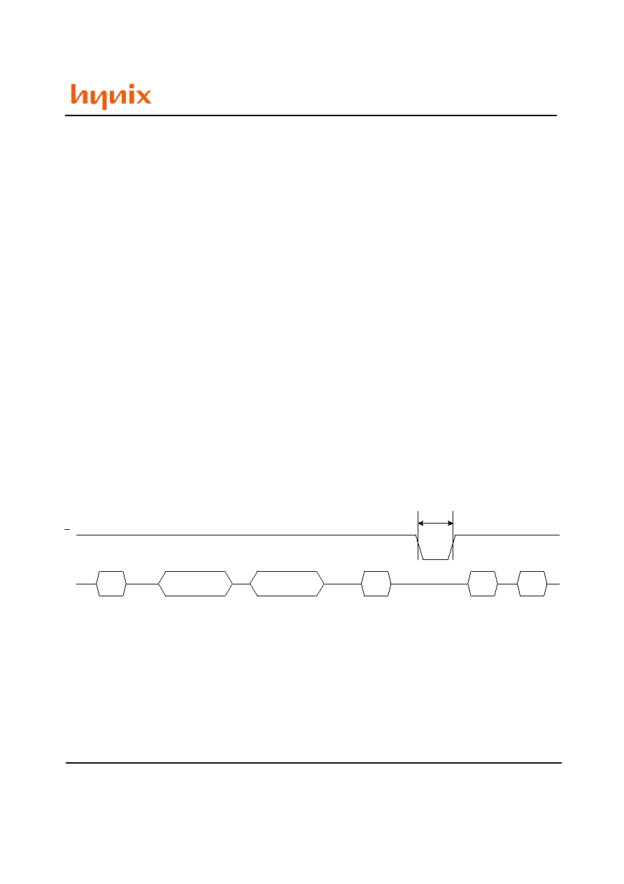
Sequential Row Read Disabled
If the device is delivered with Sequential row read disabled and Automatic Read Page 0 at Power-up, only the first
page (Page 0) will be automatically read after the power-on sequence. Refer to Figure 18.
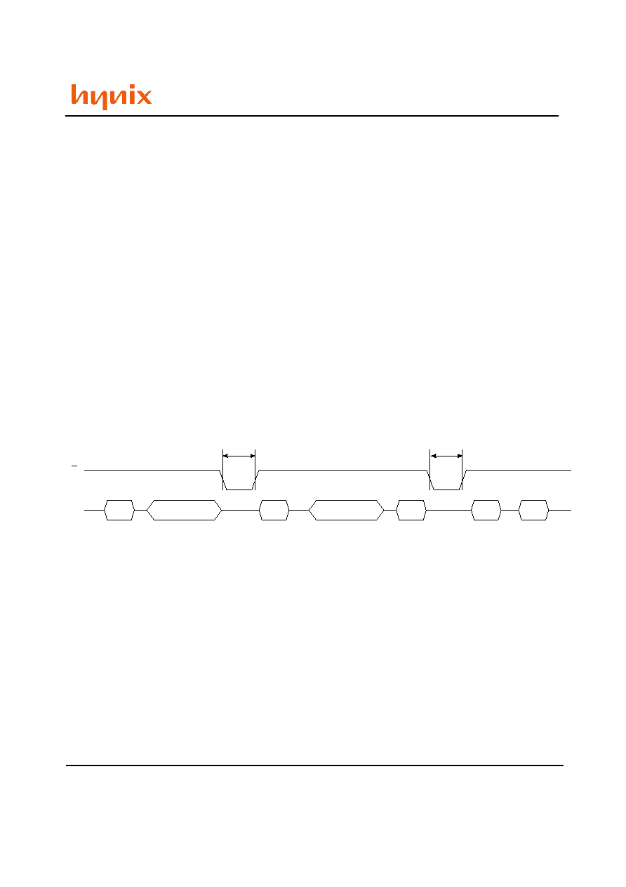
Sequential Row Read Enabled
If the device is delivered with the Automatic Page 0 Read option only (Sequential Row Read Enabled), the device will
automatically enter Sequential Row Read mode after the power-up sequence, and start reading Page 0, Page 1, etc.,
until the last memory location is reached, each new page being accessed after a time t
BLBH1
.
The Sequential Row Read operation can be inhibited or interrupted by de-asserting E (set to V
IH
) or by issuing a com-
mand. Refer to Figure 19.
Note: (1). V
CCth
is equal to 2.5V for 3.3V Power Supply devices and to 1.5V for 1.8V Power Supply devices.
Data
N+1
Data
N
Last
Data
Data
N+2
tBLBH1
Busy
Vccth (1)
Vcc
ALE
CLE
I/O
RE
RB
CE
WE
Data Output
from Address N to Last Byte or Word in Page
Figure 18. Sequential Row Read Disabled and Automatic Page 0 Read at power-up
Rev 0.6 / Oct. 2004
23
HY27SS(08/16)121M Series
HY27US(08/16)121M Series
512Mbit (64Mx8bit / 32Mx16bit) NAND Flash
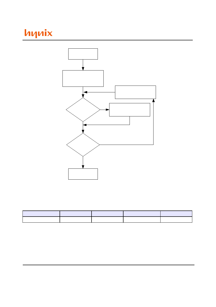
Bad Block Management
Devices with Bad Blocks have the same quality level and the same AC and DC characteristics as devices where all the
blocks are valid. A Bad Block does not affect the performance of valid blocks because it is isolated from the bit line and
common source line by a select transistor.
The devices are supplied with all the locations inside valid blocks erased (FFh). The Bad Block Information is written
prior to shipping. Any block where the 6th Byte/ 1st Word in the spare area of the 1st or 2nd page (if the 1st page is
Bad) does not contain FFh is a Bad Block.
The Bad Block Information must be read before any erase is attempted as the Bad Block Information may be erased.
For the system to be able to recognize the Bad Blocks based on the original information it is recommended to create a
Bad Block table following the flowchart shown in Figure 20.
Block Replacement
Over the lifetime of the device additional Bad Blocks may develop. In this case the block has to be replaced by copying
the data to a valid block.
These additional Bad Blocks can be identified as attempts to program or erase them will give errors in the Status Reg-
ister.
As the failure of a page program operation does not affect the data in other pages in the same block, the block can be
replaced by re-programming the current data and copying the rest of the replaced block to an available valid block.
The Copy Back Program command can be used to copy the data to a valid block.
See the "Copy Back Program" section for more details.
Refer to Table 7 for the recommended procedure to follow if an error occurs during an operation.
Table 7: Block Failure
Operation
Recommended Procedure
Erase
Block Replacement
Program
Block Replacement or ECC
Read
ECC
Note: (1). V
CCth
is equal to 2.5V for 3.3V Power Supply devices and to 1.5V for 1.8V Power Supply devices.
Figure 19. Automatic Page 0 Read at power-up (Sequential Row Read Enable)
Vccth(1)
Vcc
WE
CE
ALE
CLE
RB
I/O
tBLBH1
(Read Busy time)
Busy
Busy
Busy
Busy
tBLBH1
tBLBH1
tBLBH1
Page 0
Data Out
Page 1
Data Out
Page 2
Data Out
Page Nth
Data Out
Rev 0.6 / Oct. 2004
24
HY27SS(08/16)121M Series
HY27US(08/16)121M Series
512Mbit (64Mx8bit / 32Mx16bit) NAND Flash
Table 8: Valid Block
PROGRAM AND ERASE TIMES AND ENDURANCE CYCLES
The Program and Erase times and the number of Program/ Erase cycles per block are shown in Table 9.
Symbol
Para.
Min
Max
Unit
N
VB
# of Valid Block
4016
4096
Blocks
Figure 20. Bad Block Management Flowchart
START
Block Address=
Block 0
Data
=FFh?
Last
block?
END
Update
Bad Block table
Increment
Block Address
YES
NO
YES
NO
Rev 0.6 / Oct. 2004
25
HY27SS(08/16)121M Series
HY27US(08/16)121M Series
512Mbit (64Mx8bit / 32Mx16bit) NAND Flash
Table 9: Program, Erase Time and Program Erase Endurance Cycles
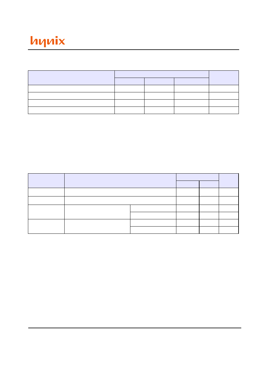
MAXIMUM RATING
Stressing the device above the ratings listed in Table 10, Absolute Maximum Ratings, may cause permanent damage to
the device. These are stress ratings only and operation of the device at these or any other conditions above those indi-
cated in the Operating sections of this specification is not implied. Exposure to Absolute Maximum Rating conditions
for extended periods may affect device reliability.
Table 10: Absolution Maximum Rating
Note: (1). Minimum Voltage may undershoot to -2V for less than 20ns during transitions on input and I/O pins. Maximum voltage
may overshoot to V
CC
+ 2V for less than 20ns during transitions on I/O pins.
DC AND AC PARAMETERS
This section summarizes the operating and measurement conditions, and the DC and AC characteristics of the device.
The parameters in the DC and AC characteristics Tables that follow, are derived from tests performed under the Mea-
surement Conditions summarized in Table 11, Operating and AC Measurement Conditions. Designers should check that
the operating conditions in their circuit match the measurement conditions when relying on the quoted parameters.
Parameters
NAND Flash
Unit
Min
Typ
Max
Page Program Time
200
500
us
Block Erase Time
2
3
ms
Program/Erase Cycles (per block)
100,000
cycles
Data Retention
10
years
Symbol
Parameter
NAND Flash
Unit
Min
Max
T
BIAS
Temperature Under Bias
-50
125
o
C
T
STG
Storage Temperature
-65
150
o
C
V
IO
(1)
Input or Output Voltage
1.8V devices
-0.6
2.7
V
3.3 V devices
-0.6
4.6
V
V
CC
Supply Voltage
1.8V devices
-0.6
2.7
V
3.3 V devices
-0.6
4.6
V
Rev 0.6 / Oct. 2004
26
HY27SS(08/16)121M Series
HY27US(08/16)121M Series
512Mbit (64Mx8bit / 32Mx16bit) NAND Flash
Table 11: Operating and AC Measurement Conditions
Note : (1). TBD
Table 12: Capacitance
Note: T
A
= 25
o
C, f = 1 MHz. C
IN
and C
I/O
are not 100% tested.
Parameter
NAND Flash
Unit
Min
Max
Supply Voltage (V
CC
)
1.8V devices
1.7
1.95
V
2.6V devices
(1)
2.4
2.8
V
3.3V devices
2.7
3.6
V
Ambient Temperature (T
A
)
Commercial Temp.
0
70
o
C
Indurstrial Temp.
-40
85
o
C
Load Capacitance (C
L
) (1 TTL GATE and C
L
)
1.8V devices
30
pF
2.6V devices
(1)
30
pF
3.3V devices
100
pF
Input Pulses Voltages
1.8V devices
0
V
CC
V
2.6V devices
(1)
0
V
CC
V
3.3V devices
0.4
2.4
V
Input and Output Timing Ref. Voltages
1.8V devices
V
CC
/2
V
2.6V devices
(1)
V
3.3V devices
1.5
V
Input Rise and Fall Times
5
ns
Symbol
Parameter
Test Condition
Typ
Max
Unit
C
IN
Input Capacitance
V
IN
= 0V
10
pF
C
I/O
Input/Output Capacitance
V
IL
= 0V
10
pF
Rev 0.6 / Oct. 2004
27
HY27SS(08/16)121M Series
HY27US(08/16)121M Series
512Mbit (64Mx8bit / 32Mx16bit) NAND Flash
Table 13: DC Characteristics, 3.3V Device and 1.8V Device
Sym-
bol
Parameter
Test Condition
3.3V Device
1.8V Device
Unit
Min
Typ
Max
Min
Typ
Max
I
CC1
Operating
Current
Sequentia
Read
t
RLRL
minimum
CE=V
IL
, I
OUT
= 0 mA
-
10
20
-
8
15
mA
I
CC2
Program
-
-
10
20
-
8
15
mA
I
CC3
Erase
-
-
10
20
-
8
15
mA
I
CC4
Stand-by Current (TTL)
CE=V
IH
, WP=0V/V
CC
-
-
1
-
-
1
mA
I
CC5
Stand-By Current
(CMOS)
CE=V
CC
-0.2,
WP=0/V
CC
-
10
50
-
10
50
uA
I
LI
Input Leakage Current
V
IN
= 0 to V
CC
max
-
-
�
10
-
-
�
10
uA
I
LO
Output Leakage Current
V
OUT
= 0 to V
CC
max
-
-
�
10
-
-
�
10
uA
V
IH
Input High Voltage
-
2.0
-
V
CC
+0.3
V
CC
-0.4
V
CC
+0.3
V
V
IL
Input Low Voltage
-
-0.3
-
0.8
-0.3
0.4
V
V
OH
Output High Voltage Level
3.3V I
OH
= -400uA
2.4
-
-
V
CC
-0.1
-
-
V
1.8V I
OH
= -100uA
V
OL
Output Low Voltage Level
3.3V I
OL
= 2.1mA
-
-
0.4
-
-
0.1
V
1.8V I
OL
= 100uA
I
OL
(RB)
Output Low Current (RB)
3.3V V
OL
= 0.4V
8
10
-
3
4
-
mA
1.8V V
OL
= 0.1V
V
LKO
V
DD
Supply Voltage
(Erase and Program
lockout)
-
-
-
2.5
-
-
1.5
V
Rev 0.6 / Oct. 2004
28
HY27SS(08/16)121M Series
HY27US(08/16)121M Series
512Mbit (64Mx8bit / 32Mx16bit) NAND Flash
Table 14: AC Characteristics for Command, Address, Data Input (3.3V and 1.8V Device)
Note: 1. If t
ELWL
is less than 10ns, t
WLWH
must be minimum 35ns, otherwise, t
WLWH
may be minimum 25ns.
Symbol
Alt.
Symbol
Parameter
3.3V
Device
1.8V
Device
Unit
t
ALLWL
t
ALS
Address Latch Low to Write Enable Low
ALE Setup time
Min
0
ns
t
ALHWL
Address Latch Hith to Write Enable Low
t
CLHWL
t
CLS
Command Latch High to Write Enable Low
CL Setup time
Min
0
ns
t
CLLWL
Command Latch Low to Write Enable Low
t
DVWH
t
DS
Data Valid to Write Enable High
Data Setup time
Min
20
ns
t
ELWL
t
CS
Chip Enable Low to Write Enable Low
CE Setup time
Min
0
ns
t
WHALH
t
ALH
Write Enable High to Address Latch High
ALE Hold time
Min
10
ns
t
WHALL
Write Enable High to Address Latch Low
t
WHCLH
t
CLH
Write Enable High to Command Latch High
CLE hold time
Min
10
ns
t
WHCLL
Write Enable High to Command Latch Low
t
WHDX
t
DH
Write Enable High to Data Transition
Data Hold time
Min
10
ns
t
WHEH
t
CH
Write Enable High to Chip Enable High
CE Hold time
Min
10
ns
t
WHWH
t
WH
Write Enable High to Write Enable Low
WE High Hold time
Min
15
20
ns
t
WLWH
t
WP
Write Enable Low to Write Enable High
WE Pulse Width
Min
25
(1)
60
ns
t
WLWL
t
WC
Write Enable Low to Write Enable Low
Write Cycle time
Min
50
80
ns
Rev 0.6 / Oct. 2004
29
HY27SS(08/16)121M Series
HY27US(08/16)121M Series
512Mbit (64Mx8bit / 32Mx16bit) NAND Flash
Table 15: AC Characteristics for Operation (3.3V Device and 1.8V Device)
Alt.
Sym-
bol
Sym-
bol
Parameter
3.3V
Device
1.8V
Device
Unit
t
ALLRL1
t
AR1
Address Latch Low to Read Enable
Low
Read Electronic Signature
Min
10
25
ns
t
ALLRL2
t
AR2
Read cycle
Min
50
80
ns
t
BHRL
t
RR
Ready/Busy High to Read Enable Low
Min
20
ns
t
BLBH1
t
R
Ready/Busy Low to Ready/Busy High
Read Busy time, 512Mb, 1Gb
4)
Max
12
15
us
t
BLBH2
t
PROG
Program Busy time
Max
500
us
t
BLBH3
t
BERS
Erase Busy time
Max
3
ms
t
BLBH4
t
RST
Reset Busy time, during ready
Max
5
us
Reset Busy time, during read
Max
5
us
Reset Busy time, during program
Max
10
us
Reset Busy time, during erase
Max
500
us
t
CLLRL
t
CLR
Command Latch Low to Read Enable Low
Min
10
ns
t
DZRL
t
IR
Data Hi-Z to Read Enable Low
Min
0
ns
t
EHBH
t
CRY
Chip Enable High to Ready/Busy High (CE intercepted read)
Max
70+tr
(1)
ns
t
EHEL
t
CEH
Chip Enable High to Chip Enable Low
(2)
Min
100
ns
t
EHQZ
t
CHZ
Chip Enable High to Output Hi-Z
Max
20
ns
t
ELQV
t
CEA
Chip Enable Low to Output Valid
Max
45
75
ns
t
RHBL
t
RB
Read Enable High to Ready/Busy Low
Max
100
ns
t
RHRL
t
REH
Read Enable High to Read Enable
Low
Read Enable High Hold time
Min
15
20
ns
t
RHQZ
t
RHZ
Read Enable High to Output Hi-Z
Min
15
ns
Max
30
t
RLRH
t
RP
Read Enable Low to Read Enable
High
Read Enable Pulse Width
Min
30
60
ns
t
RLRL
t
RC
Read Enable Low to Read Enable Low
Read Cycle time
Min
50
80
ns
t
RLQV
t
REA
Read Enable Low to Output Valid
Read Enable Access time
Max
35
60
ns
t
READID
Read ES Access time
45
t
WHBH
t
R
Write Enable High to Ready/Busy High
Max
12
15
us
t
WHBL
t
WB
Write Enable High to Ready/Busy Low
Max
100
ns
Rev 0.6 / Oct. 2004
30
HY27SS(08/16)121M Series
HY27US(08/16)121M Series
512Mbit (64Mx8bit / 32Mx16bit) NAND Flash
Note: (1). The time to Ready depends on the value of the pull-up resistor tied to the Ready/Busy pin. See Figures 32, 33 and 34.
(2). To break the sequential read cycle, CE must be held High for longer than t
EHEL
.
(3). ES = Electronic Signature.
(4). 1G DDP
t
WHRL
t
WHR
Write Enable High to Read Enable Low
Min
60
ns
t
WLWL
t
WC
Write Enable Low to Write Enable
Low
Write Cycle time
Min
50
80
ns
Alt.
Sym-
bol
Sym-
bol
Parameter
3.3V
Device
1.8V
Device
Unit
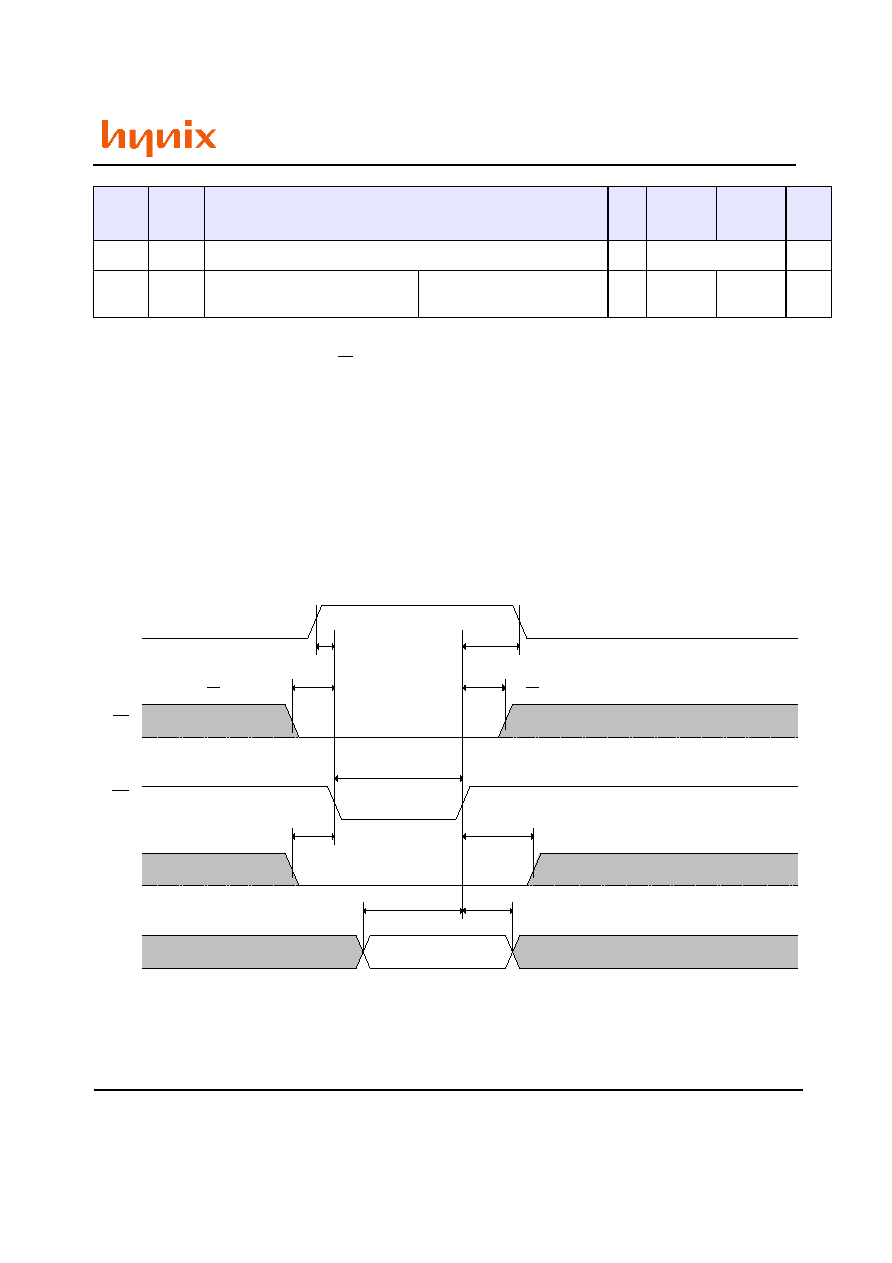
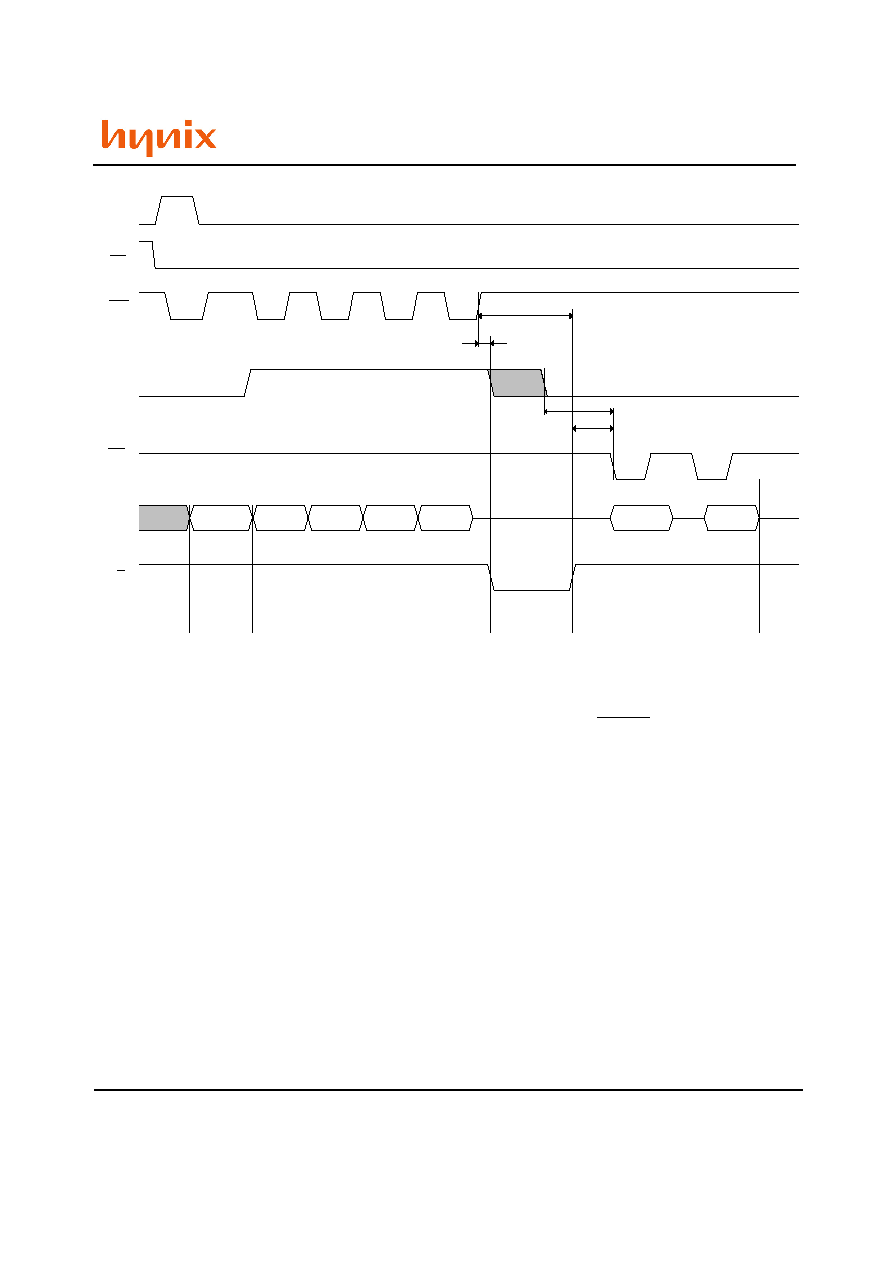
Figure 21. Command Latch AC Waveforms
Command
tCLHWL
(CLE Setup time)
tHWCLL
(CLE Hold time)
tELWL
(CE Setup time)
tWHEH
(CE Hold time)
tWLWH
tALLWL
(ALE Setup time)
tWHALH
(ALE Hold time)
tDVWH
(Data Setup time)
tWHDX
(Data Hold time)
CLE
ALE
I/O
CE
WE
Rev 0.6 / Oct. 2004
31
HY27SS(08/16)121M Series
HY27US(08/16)121M Series
512Mbit (64Mx8bit / 32Mx16bit) NAND Flash
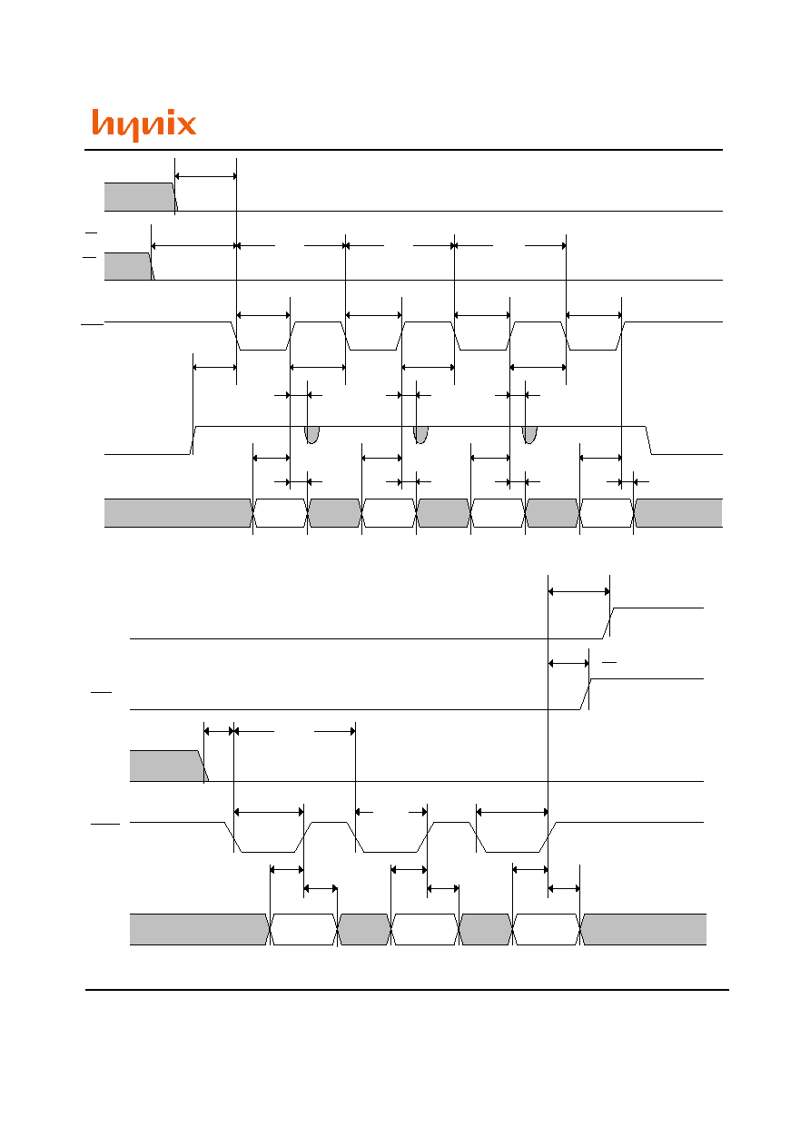
Figure 22. Address Latch AC Waveforms
Figure 23. Data Input Latch AC Waveforms
I/O
WE
CE
CLE
ALE
Address
cycle 1
Address
cycle 3
Address
cycle 2
Address
cycle 4
tCLLWL
(CLE Setup time)
tELWL
(CE Setup time)
tWLWL
tWLWL
tWLWL
tWLWH
tWLWH
tWLWH
tWLWH
tALHWL
(ALE Setup time)
tWHWL
tWHWL
tWHWL
tWHALL
(ALE Hold time)
tWHALL
tWHALL
tDVWH
(Data Setup time)
tDVWH
tDVWH
tDVWH
tWHDX
(Data Hold time)
tWHDX
tWHDX
tWHDX
I/O
WE
CE
Data In 0
Data In 1
Data In
Last
tWHCLH
(CLE Hold time)
tWHEH
(CE Hold time)
tWLWH
tWLWL
tALLWL
(ALE Setup time)
tWLWH
tWLWH
tDVWH
(Data Setup time)
tDVWH
tDVWH
tWHDX
(Data Hold time)
tWHDX
tWHDX
CLE
ALE
Rev 0.6 / Oct. 2004
32
HY27SS(08/16)121M Series
HY27US(08/16)121M Series
512Mbit (64Mx8bit / 32Mx16bit) NAND Flash
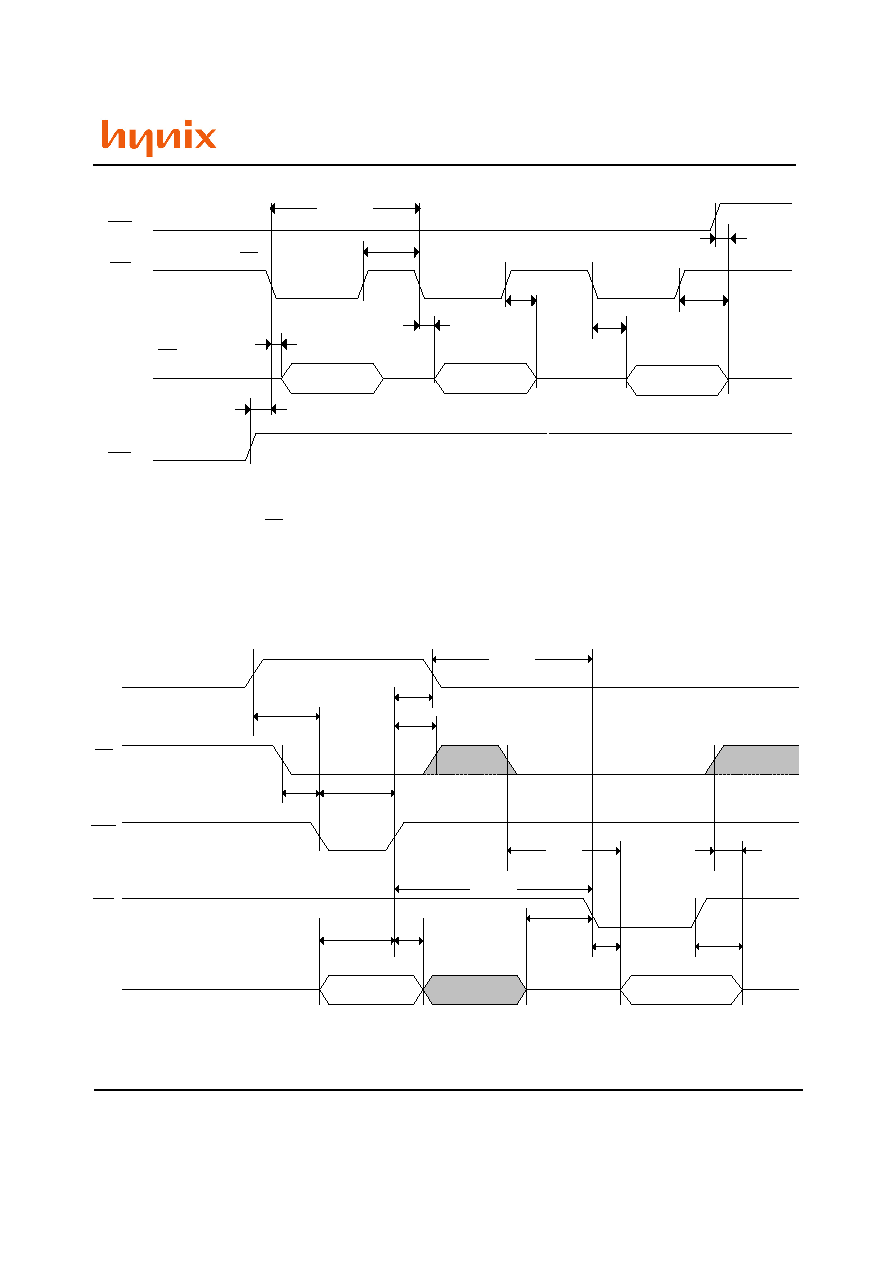
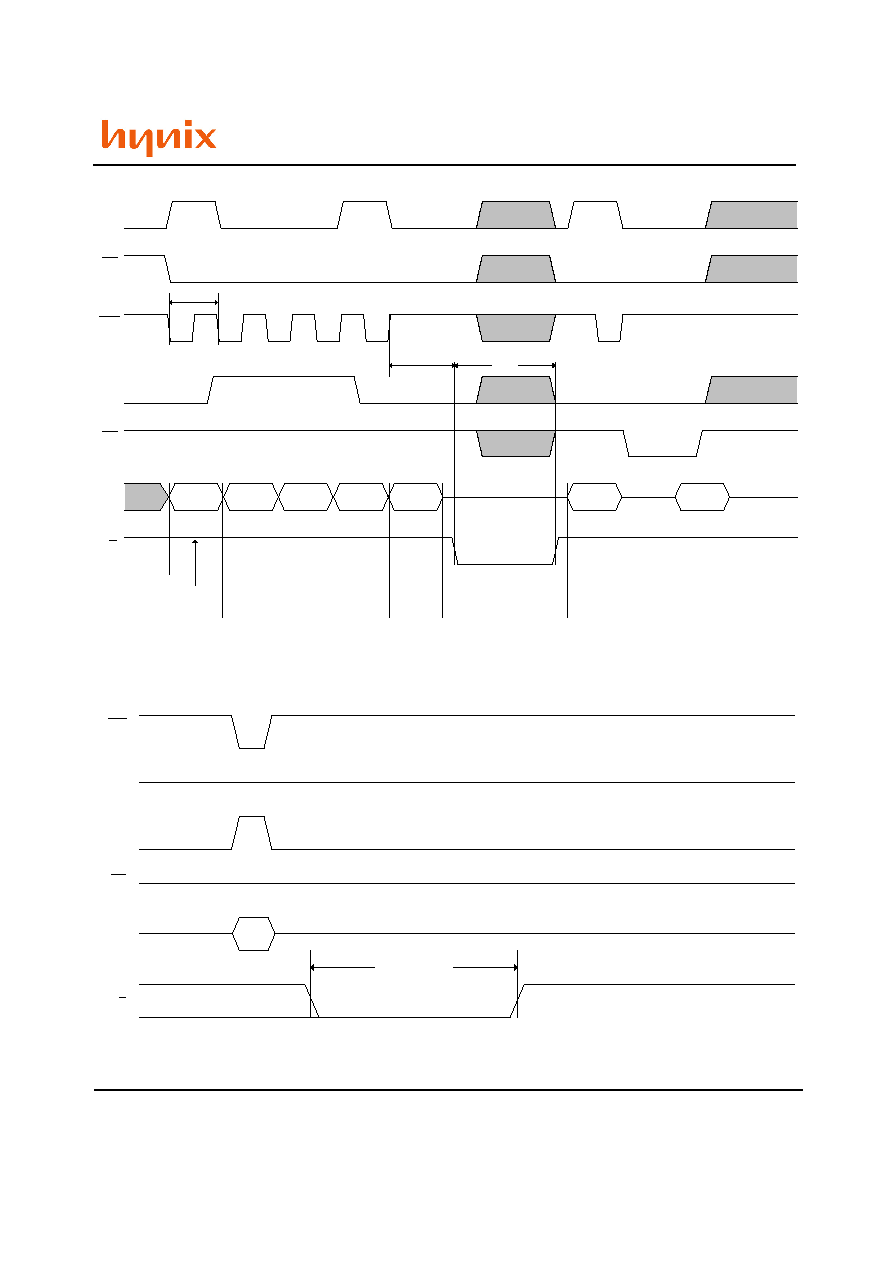
Note:1. CLE = Low, ALE = Low, WE = High.
Figure 24. Sequential Data Output after Read AC Waveforms
Figure 25. Read Status Register AC Waveform
I/O
RE
RB
Data Out
Data Out
Data Out
tRLRL
(Read Cycle time)
tEHQZ
tRHQZ
tRLQV
tRHQZ
tRLQV
tBHRL
tRHRL
(RE High Holdtime)
tRLQV
(RE Accesstime)
CE
I/O
RE
CE
WE
CLE
Status Register
Output
70h
tCLLRL
tWHCLL
tWHEH
tCLHWL
tELWL
tWLWH
tELQV
tWHRL
tEHQZ
tRHQZ
tRLQV
tDZRL
tDVWH
(Data Setup time)
tWHDX
(Data Hold time)
Rev 0.6 / Oct. 2004
33
HY27SS(08/16)121M Series
HY27US(08/16)121M Series
512Mbit (64Mx8bit / 32Mx16bit) NAND Flash
Note: Refer to table(To see Page 22) for the values of the manufacture and device codes.
Figure 26. Read Electronic Signature AC Waveform
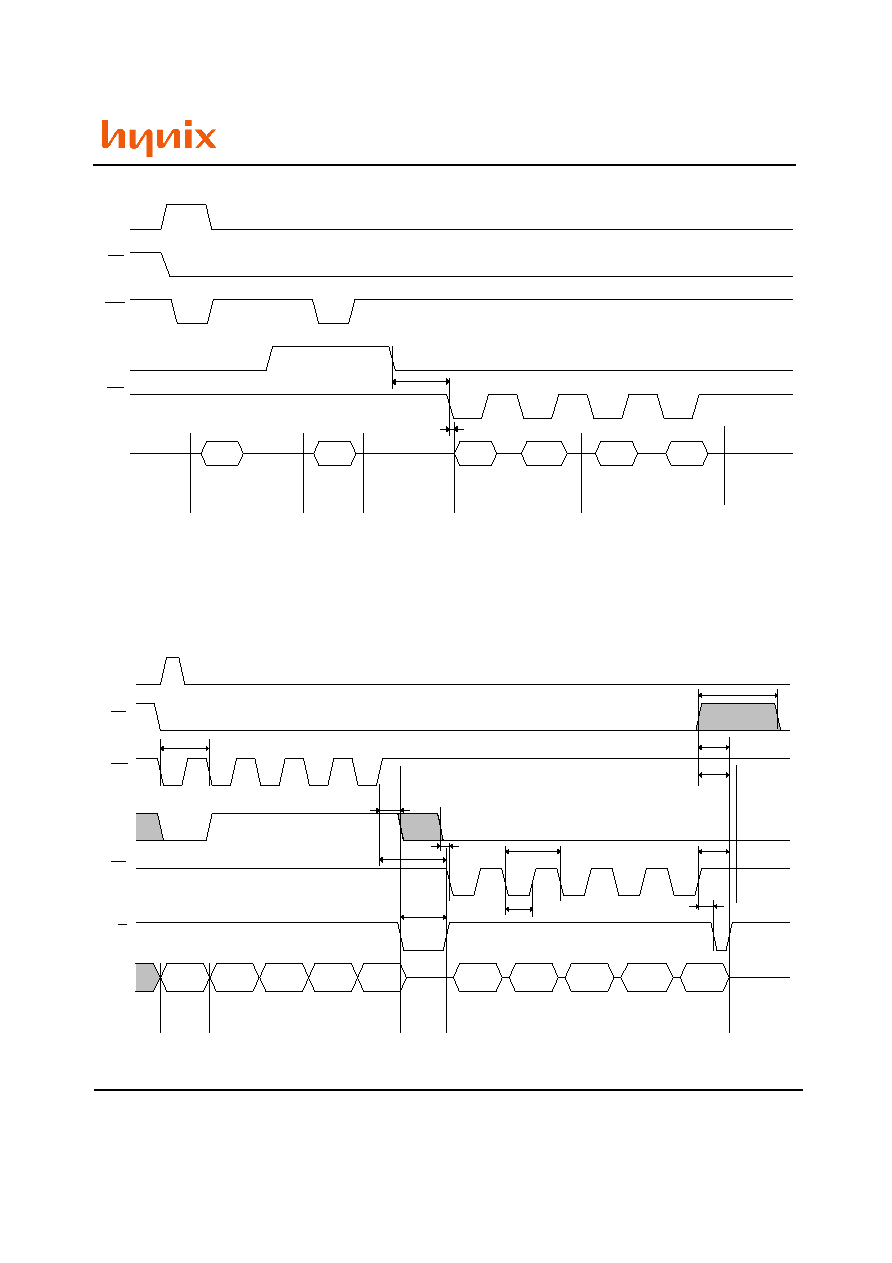
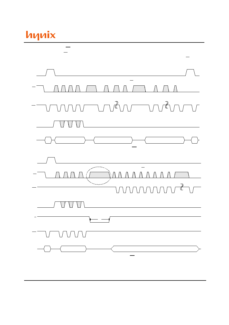
Figure 27. Read Read A/ Read B Operation AC Waveform
I/O
RE
CE
Man.
code
90h
Device
code
Don't
Care
Don't
Care
00h
WE
ALE
CLE
Read Electronic
Signature Command
1st Cycle
Address
Manufacturer and
Device Code
Reserved For
Future Use
tALLRL1
tRLQV
(Read ES Access time)
I/O
RE
CE
WE
ALE
CLE
RB
Busy
Data Output
from Address N to Last Byte or Word in Page
Data
N
Add.N
cycle 1
Add.N
cycle 2
Add.N
cycle 3
Add.N
cycle 4
00h or
01h
Data
N+1
Data
N+2
Data
Last
Address N Input
Command
Code
tEHEL
tWHWL
tWHBL
tWHBH
tALLRL2
tRLRL
(Read Cycle time)
tRHQZ
tRHBL
tRLRH
tBLBH1
tEHQZ
tEHBH
Rev 0.6 / Oct. 2004
34
HY27SS(08/16)121M Series
HY27US(08/16)121M Series
512Mbit (64Mx8bit / 32Mx16bit) NAND Flash
Note: 1. A0-A7 is the address in the Spare Memory area, where A0-A3 are valid and A4-A7 are don't care.
2. Only address cycle 4 is required.
Figure 28. Read C Operation, One Page AC Waveform
I/O
WE
CE
CLE
ALE
RE
RB
Add. M
cycle 1
50h
Data M
Add. M
cycle 2
Add. M
cycle 3
Add. M
cycle 4
Data
Last
tWHBH
tWHALL
tBHRL
tALLRL2
Command
Code
Address M Input
Busy
Data Output from M to
Last Byte or Word in Area C
Rev 0.6 / Oct. 2004
35
HY27SS(08/16)121M Series
HY27US(08/16)121M Series
512Mbit (64Mx8bit / 32Mx16bit) NAND Flash
Figure 29. Page Program AC Waveform
I/O
WE
CE
CLE
ALE
RE
RB
N
Last
10h
70h
SR0
tWLWL
(Write Cycle time)
tWLWL
tWLWL
tWHBL
tBLBH2
(Program Busy time)
Address Input
Data Input
Confirm
Code
Page
Program
Read Status
Register
80h
Add. N
cycle 1
Add. N
cycle 2
Add. N
cycle 3
Page Program
Setup Code
Rev 0.6 / Oct. 2004
36
HY27SS(08/16)121M Series
HY27US(08/16)121M Series
512Mbit (64Mx8bit / 32Mx16bit) NAND Flash
Figure 30. Block Erase AC Waveform
Figure 31. Reset AC Waveform
I/O
WE
CE
CLE
ALE
RE
RB
70h
SR0
60h
Add. N
cycle 1
Add. N
cycle 2
Add. N
cycle 3
D0h
tBLBH3
(Erase Busy time)
tWLWL
(Write Cycle time)
Block Erase
Setup Command
Block Address Input
Confirm
Code
Block Erase
Read Status Register
FFh
tBLBH4
(Reset Busy time)
ALE
I/O
RE
WE
CLE
RB
Rev 0.6 / Oct. 2004
37
HY27SS(08/16)121M Series
HY27US(08/16)121M Series
512Mbit (64Mx8bit / 32Mx16bit) NAND Flash
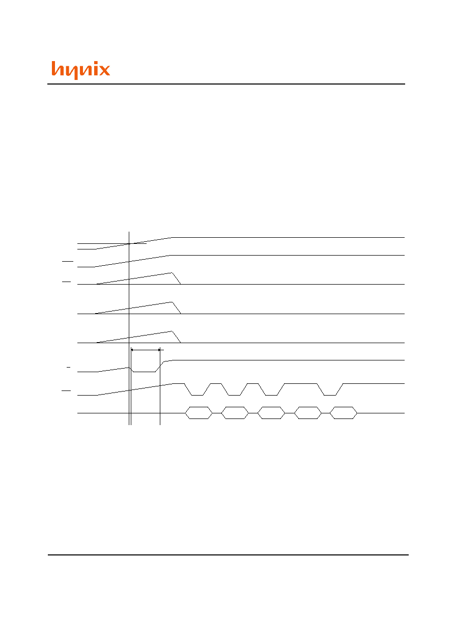
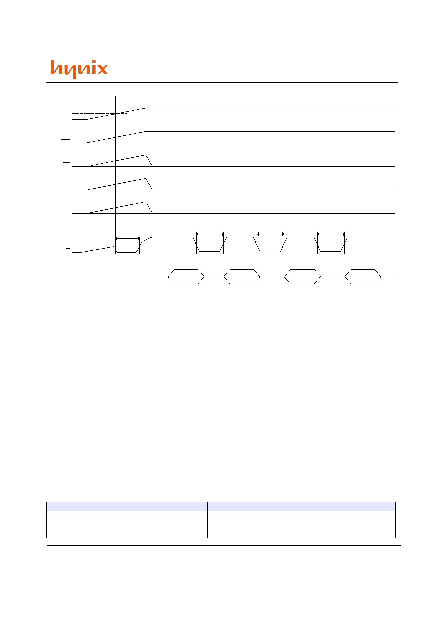
System Interface Using CE don't care
To simplify system interface, CE may be deasserted during data loading or sequential data-reading as shown below. So, it is possible
to connect NAND Flash to a microprocessor. The only function that was removed from standard NAND Flash to make CE don't care
read operation was disabling of the automatic sequential read function.
Figure 32. Program Operation with CE don't-care
.
Figure 33. Read Operation with CE don't-care.
CLE
ALE
I/Ox
CE
WE
CE don't-care
tR
00h
Start Add(4Cycle)
Data Output(sequential)
RE
R/B
If sequential row read enabled,
CE must be held low during tR.
CLE
CE don't-care
CE
WE
ALE
80h
Start Add(4Cycle)
Data Input
Data Input
10h
I/Ox
Rev 0.6 / Oct. 2004
38
HY27SS(08/16)121M Series
HY27US(08/16)121M Series
512Mbit (64Mx8bit / 32Mx16bit) NAND Flash
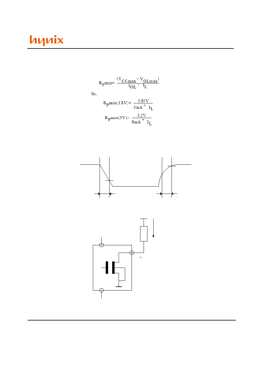
Ready/Busy Signal Electrical Characteristics
Figures 32, 33 and 34 show the electrical characteristics for the Ready/Busy signal. The value required for the resistor
R
P
can be calculated using the following equation:
where I
L
is the sum of the input currents of all the devices tied to the Ready/Busy signal. R
P
max is determined by the
maximum value of tr.
Figure 34. Ready/Busy AC Waveform
Figure 35. Ready/Busy Load Circuit
ready
V
OL
Vcc
V
OH
tr
tf
busy
Vcc
Device
Vss
Rp
ibusy
RB
Open Drain Output
Rev 0.6 / Oct. 2004
39
HY27SS(08/16)121M Series
HY27US(08/16)121M Series
512Mbit (64Mx8bit / 32Mx16bit) NAND Flash
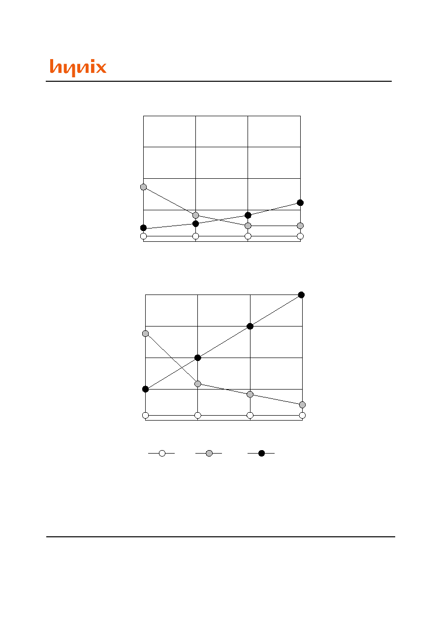
Figure 36. Resistor Value Waveform Timings for Ready/Busy Signal
400
300
200
100
0
1
2
3
4
1.7
1
2
3
4
1.7
1.7
1.7
1.7
30
60
90
120
0.85
0.57
0.43
Vcc=1.8, CL=30pF
Rp(K)
tr, tf(ns)
ib
usy(mA
)
400
300
200
100
0
1
2
3
4
3.6
1
2
3
4
3.6
3.6
2.4
3.6
100
1.2
0.8
400
200
300
0.6
Vcc=3.3, CL=100pF
Rp(K)
tr, tf(ns)
ib
usy(mA
)
tf
ibusy
tr
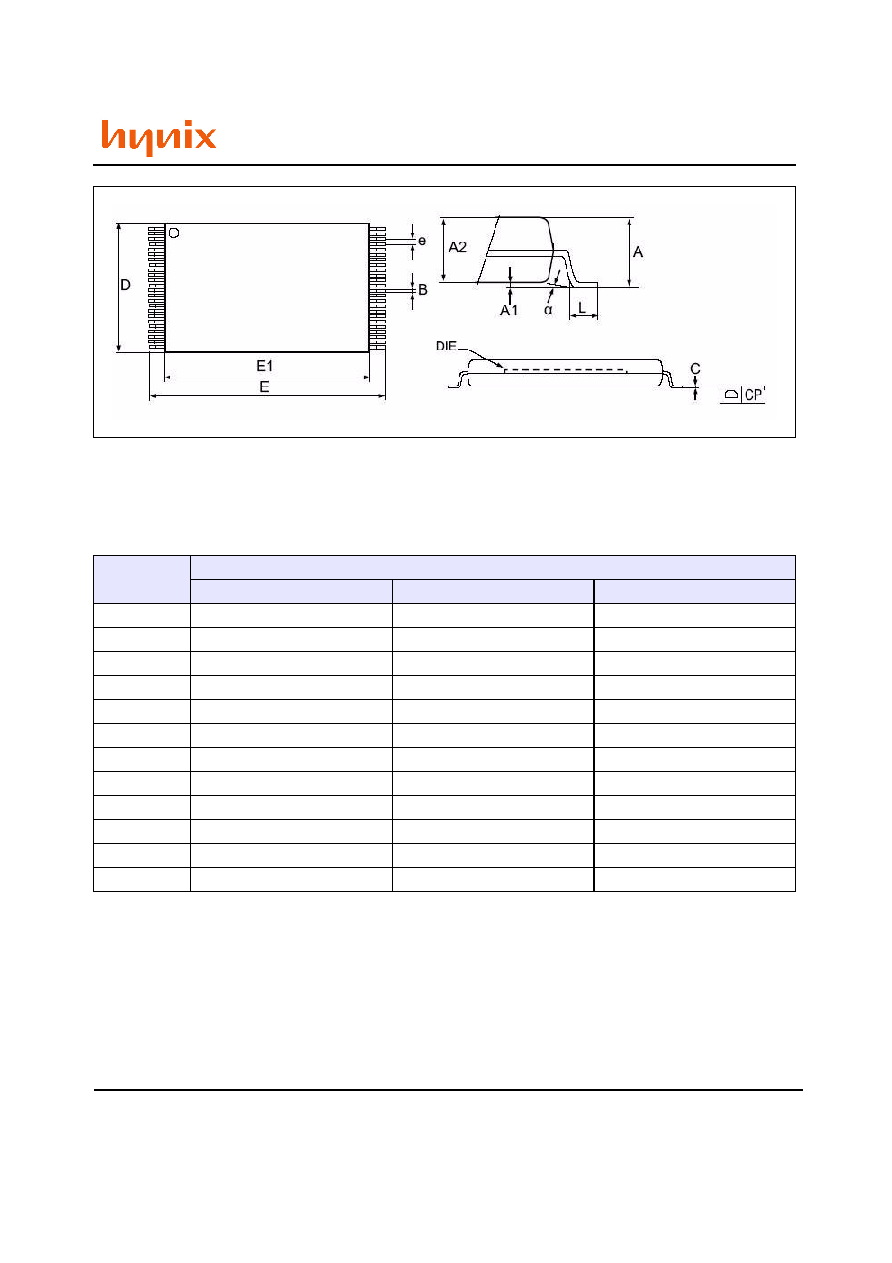
Rev 0.6 / Oct. 2004
40
HY27SS(08/16)121M Series
HY27US(08/16)121M Series
512Mbit (64Mx8bit / 32Mx16bit) NAND Flash
Table 16: 48-TSOP1 - 48-lead Plastic Thin Small Outline, 12 x 20mm, Package Mechanical Data
Symbol
millimeters
Min
Typ
Max
A
1.200
A1
0.050
0.150
A2
0.980
1.030
B
0.170
0.250
C
0.100
0.200
CP
0.050
D
11.910
12.000
12.120
E
19.900
20.000
20.100
E1
18.300
18.400
18.500
e
0.500
L
0.500
0.680
alpha
0
5
Figure 37. 48-TSOP1 - 48-lead Plastic Thin Small Outline, 12 x 20mm, Package Outline
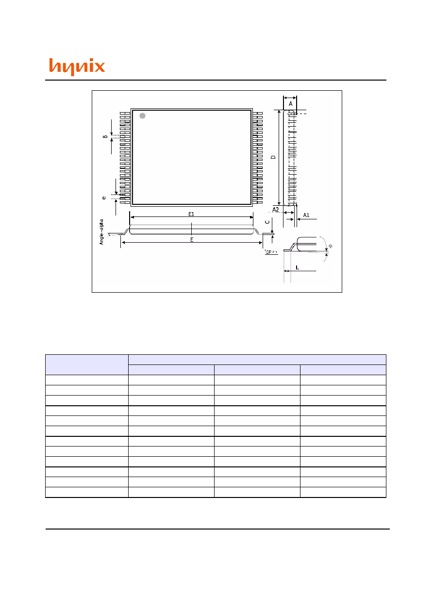
Rev 0.6 / Oct. 2004
41
HY27SS(08/16)121M Series
HY27US(08/16)121M Series
512Mbit (64Mx8bit / 32Mx16bit) NAND Flash
Table 17: 48-WSOP1 - 48-lead Plastic Thin Small Outline, 12 x 17mm, Package Mechanical Data
Symbol
millimeters
Min
Typ
Max
A
0.700
A1
0
0.080
A2
0.540
0.620
B
0.130
0.230
C
0.065
0.175
CP
0.050
D
11.910
12.000
12.120
D
16.900
17.000
17.100
E
15.300
15.400
15.500
e
0.500
L
0.450
0.750
alpha
0
Figure 38. 48-WSOP1 - 48-lead Plastic Very Very Thin Small Outline, 12 x 17mm, Package Outline
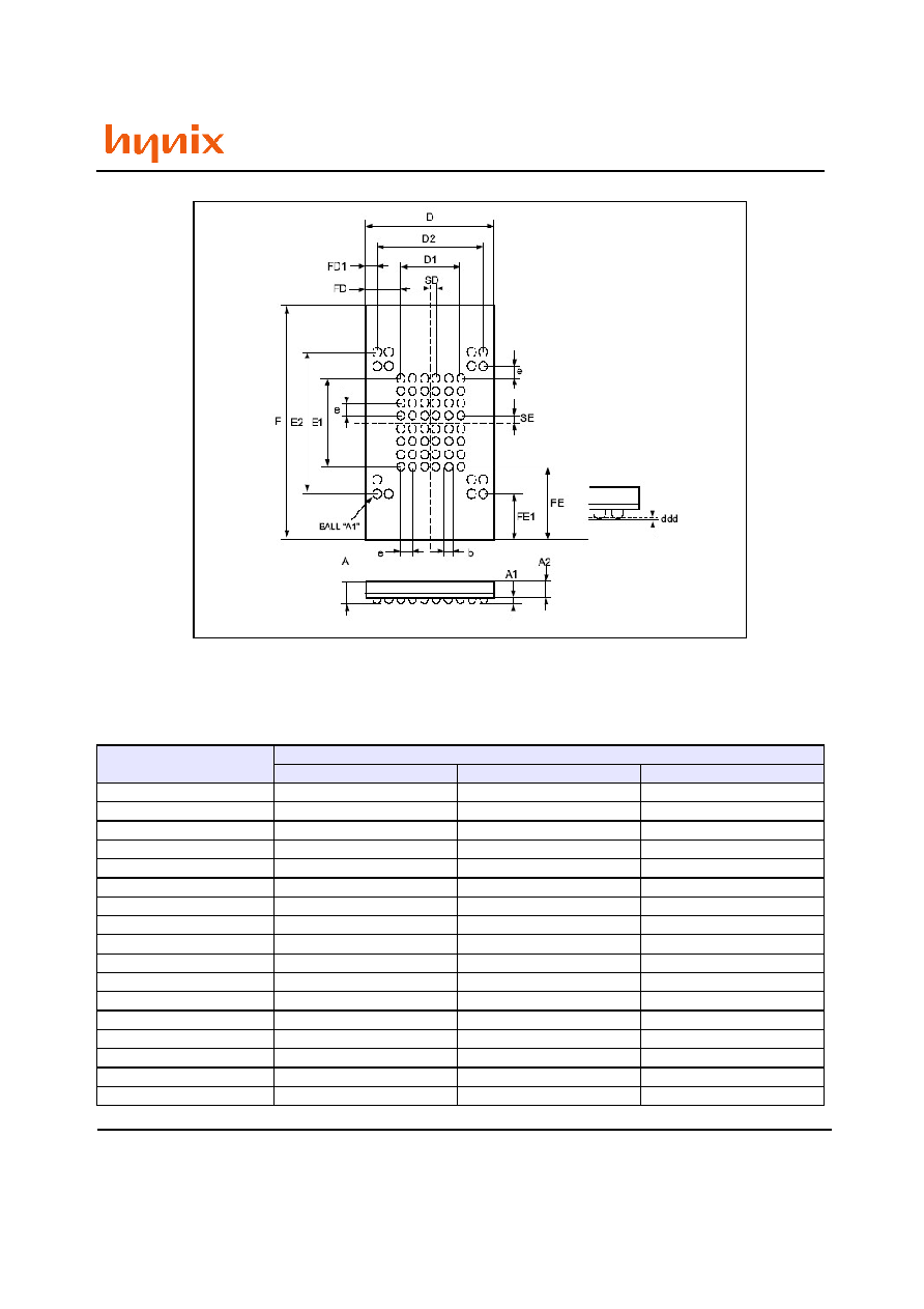
Rev 0.6 / Oct. 2004
42
HY27SS(08/16)121M Series
HY27US(08/16)121M Series
512Mbit (64Mx8bit / 32Mx16bit) NAND Flash
Table 17: 48-WSOP1 - 48-lead Plastic Thin Small Outline, 12 x 17mm, Package Mechanical Data
Symbol
millimeters
Min
Typ
Max
A
1.00
1.10
1.20
A1
0.21
0.26
0.31
A2
0.79
0.84
0.89
b
0.40
0.45
0.50
D
8.40
8.50
8.60
D1
4.00
D2
7.20
E
14.90
15.00
15.10
E1
5.60
E2
8.80
e
0.80
FD
2.25
FD1
0.65
FE
4.70
FE1
3.10
SD
0.40
SE
0.40
Figure 39. 63-FBGA - 8.5 x 15mm, 6x8 ball array 0.8mm pitch, Pakage Outline
Note: Drawing is not to scale.
Rev 0.6 / Oct. 2004
43
HY27SS(08/16)121M Series
HY27US(08/16)121M Series
512Mbit (64Mx8bit / 32Mx16bit) NAND Flash
MARKING INFORMATION
Package
Marking Example
TSOP1
/
WSOP1
/
FBGA
K
O
R
H
Y
2
7
x
S
x
x
1
2
1
M
x
x
x
x
Y
W
W
x
x
- hynix
- KOR
- HY27xSxx121mTxB
HY: HYNIX
27: NAND Flash
x: Power Supply
S: Classification
xx: Bit Organization
12: Density
1: Mode
M: Version
x: Package Type
x: Package Material
x: Operating Temperature
x: Bad Block
- Y: Year (ex: 4=year 2004, 05= year 2005)
- ww: Work Week (ex: 12= work week 12)
- xx: Process Code
Note
- Capital Letter
- Small Letter
: Hynix Symbol
: Origin Country
: U(2.7V~3.6V), S(1.7V~2.2V)
: Single Level Cell+Single Die
: 08(x8), 16(x16)
: 512Mb
: 1nCE & 1R/nB; CE don't care
: 1st Generation
: T(TSOP1), V(WSOP1), F(FBGA)
: Blank(Normal), P(Lead Free)
: C(0~70), E(-25~85)
I(-40~85)
: B(Included Bad Block), S(1~5 Bad Block),
P(All Good Block)
: Fixed Item
: Non-fixed Item
: Part Number