Äîêóìåíòàöèÿ è îïèñàíèÿ www.docs.chipfind.ru
This document is a general product description and is subject to change without notice. Hynix does not assume any responsibility for
use of circuits described. No patent licenses are implied.
Rev 0.7 / Oct. 2004
1
HY27SS(08/16)561M Series
HY27US(08/16)561M Series
256Mbit (32Mx8bit / 16Mx16bit) NAND Flash
Document Title
256Mbit (32Mx8bit / 16Mx16bit) NAND Flash Memory
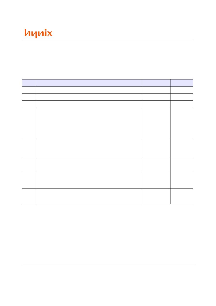
Revision History
No.
History
Draft Date
Remark
0.0
Initial Draft
Jul. 10. 2003
Preliminary
0.1
Renewal Product Group
Dec. 08. 2003
Preliminary
0.2
Append 1.8V Operation Product to Data sheet
Dec. 08. 2003
Preliminary
0.3
Insert Spare Enable function for GND Pin(#6)
- In case of Reading or Programming, GND Pin(#6) should be Low
or High.
- Change the test condition of Stand-by current-Refer to Table 13.
Change CSP Package name & thickness
- Name : VFBGA -> FBGA
- Thickness : 1.0mm(max) -> 1.2mm(max)
Mar. 08. 2004
Preliminary
0.4
1) Delete Cache Program Mode
2) Modify the description of Device Operations
- /CE Don't Care Enabled(Disabled) -> Sequential Row Read
Disabled(Enabled) (Page23)
Jun. 01. 2004
Preliminary
0.5
1) change FBGA dimension
: Thickness : 1.2mm(max) -> 1.0mm(max)
2) Edit Fig.33 read operation with CE don't care
Sep. 24. 2004
Preliminary
0.6
1) Change TSOP1,WSOP1,FBGA package dimension
- Change TSOP1,WSOP1,FBGA mechanical data
- Inches parameter has been excluded from the mechanical data table
Oct. 18. 2004
Preliminary
0.7
1) Change TSOP1, WSOP1, FBGA package dimension
2) Edit TSOP1, WSOP1 package figures
3) Change FBGA package figure
Oct. 20. 2004

This document is a general product description and is subject to change without notice. Hynix does not assume any responsibility for
use of circuits described. No patent licenses are implied.
Rev 0.7 / Oct. 2004
2
HY27SS(08/16)561M Series
HY27US(08/16)561M Series
256Mbit (32Mx8bit / 16Mx16bit) NAND Flash
FEATURES SUMMARY
HIGH DENSITY NAND FLASH MEMORIES
- Cost effective solutions for mass storage applications
NAND INTERFACE
- x8 or x16 bus width.
- Multiplexed Address/ Data
- Pinout compatibility for all densities
SUPPLY VOLTAGE
- 3.3V device: VCC = 2.7 to 3.6V : HY27USXX561M
- 1.8V device: VCC = 1.7 to 1.95V : HY27SSXX561M
Memory Cell Array
- 256Mbit = 528 Bytes x 32 Pages x 2,048 Blocks
PAGE SIZE
- x8 device : (512 + 16 spare) Bytes
: HY27US08561M
- x16 device: (256 + 8 spare) Words
: HY27US16561M
BLOCK SIZE
- x8 device: (16K + 512 spare) Bytes
- x16 device: (8K + 256 spare) Words
PAGE READ / PROGRAM
- Random access: 10us (max)
- Sequential access: 50ns (min)
- Page program time: 200us (typ)
COPY BACK PROGRAM MODE
- Fast page copy without external buffering
FAST BLOCK ERASE
- Block erase time: 2ms (Typ)
STATUS REGISTER
ELECTRONIC SIGNATURE
CHIP ENABLE DON'T CARE OPTION
- Simple interface with microcontroller
AUTOMATIC PAGE 0 READ AT POWER-UP
OPTION
- Boot from NAND support
- Automatic Memory Download
SERIAL NUMBER OPTION
HARDWARE DATA PROTECTION
- Program/Erase locked during Power transitions
DATA INTEGRITY
- 100,000 Program/Erase cycles
- 10 years Data Retention
PACKAGE
- HY27US(08/16)561M-T(P)
: 48-Pin TSOP1 (12 x 20 x 1.2 mm)
- HY27US(08/16)561M-T (Lead)
- HY27US(08/16)561M-TP (Lead Free)
- HY27US08561M-V(P)
: 48-Pin WSOP1 (12 x 17 x 0.7 mm)
- HY27US08561M-V (Lead)
- HY27US08561M-VP (Lead Free)
- HY27(U/S)S(08/16)561M-F(P)
: 63-Ball FBGA (9.0 x 11 x 1.0 mm)
- HY27US(08/16)561M-F (Lead)
- HY27US(08/16)561M-FP (Lead Free)
- HY27SS(08/16)561M-F (Lead)
- HY27SS(08/16)561M-FP (Lead Free)

Rev 0.7 / Oct. 2004
3
HY27SS(08/16)561M Series
HY27US(08/16)561M Series
256Mbit (32Mx8bit / 16Mx16bit) NAND Flash
DESCRIPTION
The HYNIX HY27(U/S)SXX561M series is a family of non-volatile Flash memories that uses NAND cell technology. The
devices operate 3.3V and 1.8V voltage supply. The size of a Page is either 528 Bytes (512 + 16 spare) or 264 Words
(256 + 8 spare) depending on whether the device has a x8 or x16 bus width.
The address lines are multiplexed with the Data Input/ Output signals on a multiplexed x8 or x16 Input/ Output bus.
This interface reduces the pin count and makes it possible to migrate to other densities without changing the footprint.
Each block can be programmed and erased over 100,000 cycles. To extend the lifetime of NAND Flash devices it is
strongly recommended to implement an Error Correction Code (ECC). A Write Protect pin is available to give a hard-
ware protection against program and erase operations.
The devices feature an open-drain Ready/Busy output that can be used to identify if the Program/ Erase/Read (PER)
Controller is currently active. The use of an open-drain output allows the Ready/ Busy pins from several memories to
be connected to a single pull-up resistor.
A Copy Back command is available to optimize the management of defective blocks. When a Page Program operation
fails, the data can be programmed in another page without having to resend the data to be programmed.
The devices are available in the following packages:
- 48-TSOP1 (12 x 20 x 1.2 mm)
- 48-WSOP1 (12 x 17 x 0.7 mm)
- 63-FBGA (9.0 x 11 x 1.0 mm, 6 x 8 ball array, 0.8mm pitch)
Three options are available for the NAND Flash family:
- Automatic Page 0 Read after Power-up, which allows the microcontroller to directly download the boot code from
page 0.
- Chip Enable Dont Care, which allows code to be directly downloaded by a microcontroller, as Chip Enable transitions
during the latency time do not stop the read operation.
- A Serial Number, which allows each device to be uniquely identified. The Serial Number options is subject to an NDA
(Non Disclosure Agreement) and so not described in the datasheet. For more details of this option contact your near-
est HYNIX Sales office.
Devices are shipped from the factory with Block 0 always valid and the memory content bits, in valid blocks, erased to
'1'.
Rev 0.7 / Oct. 2004
4
HY27SS(08/16)561M Series
HY27US(08/16)561M Series
256Mbit (32Mx8bit / 16Mx16bit) NAND Flash
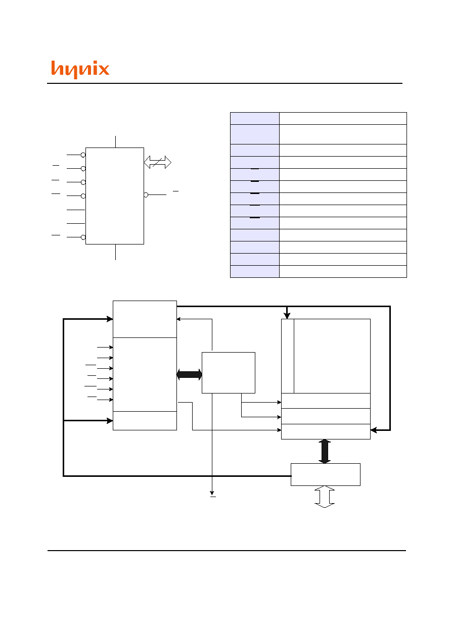
I/O
8-15
Data Input/Outputs for x16 Device
I/O
0-7
Data Input/Output, Address Inputs, or Com-
mand Inputs for x8 and x16 device
ALE
Address Latch Enable
CLE
Command Latch Enable
CE
Chip Enable
RE
Read Enable
RB
Read/Busy (open-drain output)
WE
Write Enable
WP
Write Protect
VCC
Supply Voltage
VSS
Ground
GND
GND Input for Spare Area Enable
NC
Not Connected Internally
Table 1: Signal Name
Figure 1: Logic Diagram
Figure 2. LOGIC BLOCK DIAGRAM
NAND
Flash
Vcc
Vss
ALE
CLE
CE
RE
WE
WP
I/O8-I/O15, x16
I/O0-I/O7, x8/x16
RB
GND
I/O Buffers &
Latches
Page Buffer
Cache Register
Y Decoder
NAND Flash
Memory Array
Address
Register/Counter
Command
Interface
Logic
Command Register
P/E/R
Controller,
High Voltage
Generator
X De
co
de
r
ALE
CLE
WE
CE
WP
RE
I/O0-I/O7, x8/x16
I/O8-I/O15, x16
RB
Rev 0.7 / Oct. 2004
5
HY27SS(08/16)561M Series
HY27US(08/16)561M Series
256Mbit (32Mx8bit / 16Mx16bit) NAND Flash
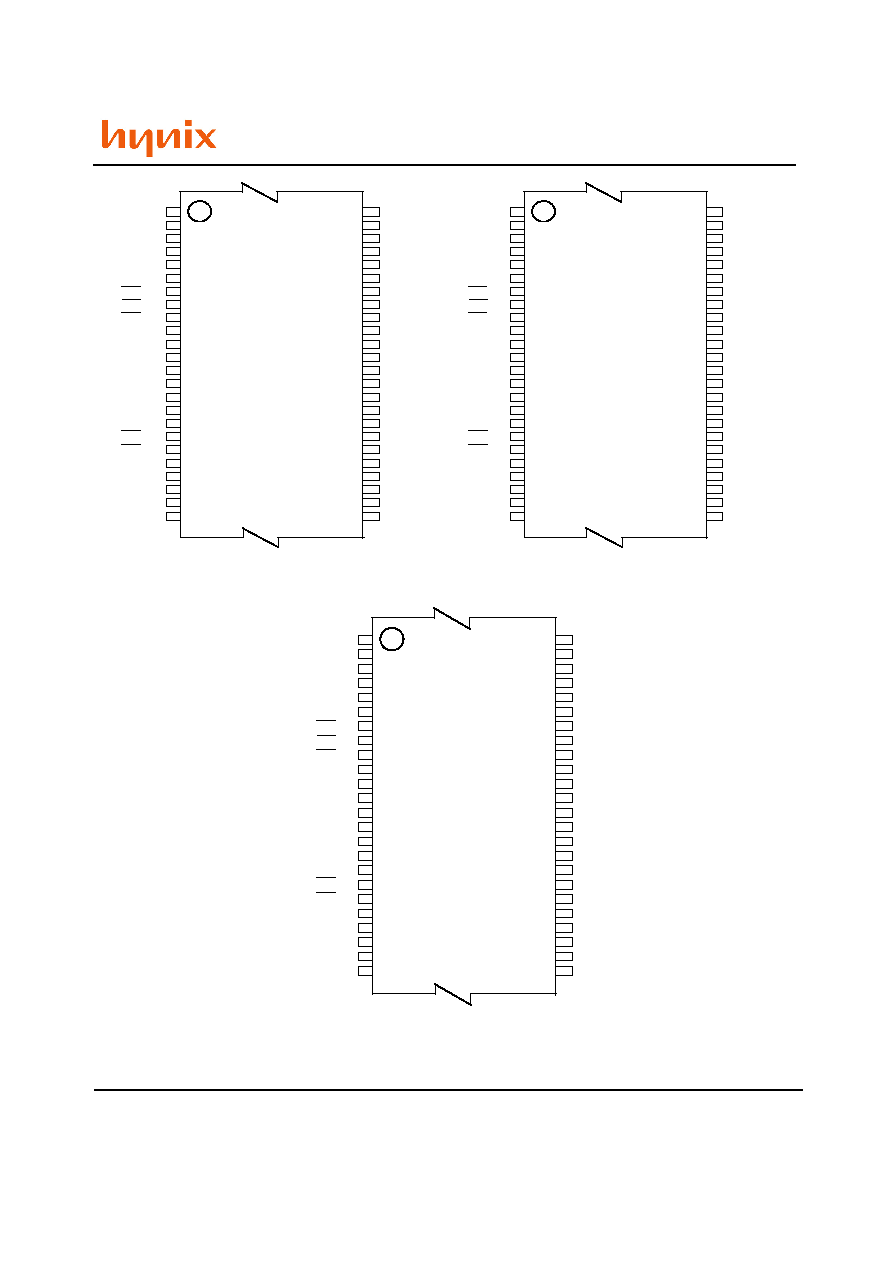
Figure 3. 48-TSOP1 Contactions, x8 and x16 Device
Figure 4. 48-WSOP1 Contactions, x8 Device
1
12
13
24
48
37
36
25
NC
NC
NC
NC
I/O7
I/O6
I/O5
I/O4
NC
NC
NC
Vcc
Vss
NC
NC
NC
I/O3
I/O2
I/O1
I/O0
NC
NC
NC
NC
NC
NC
NC
NC
NC
GND
CE
NC
NC
Vcc
Vss
NC
NC
CLE
ALE
NC
NC
NC
NC
NC
RB
RE
WE
WP
NAND Flash
(x8)
1
12
13
24
48
37
36
25
Vss
I/O15
I/O7
I/O14
I/O6
I/O13
I/O5
I/O12
I/O4
NC
NC
Vcc
NC
NC
NC
I/O11
I/O3
I/O10
I/O2
I/O9
I/O1
I/O8
I/O0
Vss
NC
NC
NC
NC
NC
GND
CE
NC
NC
Vcc
Vss
NC
NC
CLE
ALE
NC
NC
NC
NC
NC
RB
RE
WE
WP
NAND Flash
(x16)
1
12
13
24
48
37
36
25
NC
NC
NC
NC
I/O7
I/O6
I/O5
I/O4
NC
NC
NC
Vcc
Vss
NC
NC
NC
I/O3
I/O2
I/O1
I/O0
NC
NC
NC
NC
NC
NC
NC
NC
NC
GND
CE
NC
NC
Vcc
Vss
NC
NC
CLE
ALE
NC
NC
NC
NC
NC
RB
RE
WE
WP
NAND Flash
(x8)
1
12
13
24
48
37
36
25
NC
NC
NC
NC
I/O7
I/O6
I/O5
I/O4
NC
NC
NC
Vcc
Vss
NC
NC
NC
I/O3
I/O2
I/O1
I/O0
NC
NC
NC
NC
NC
NC
NC
NC
NC
GND
CE
NC
NC
Vcc
Vss
NC
NC
CLE
ALE
NC
NC
NC
NC
NC
RB
RB
RE
RE
WE
WE
WP
WP
NAND Flash
(x8)
1
12
13
24
48
37
36
25
Vss
I/O15
I/O7
I/O14
I/O6
I/O13
I/O5
I/O12
I/O4
NC
NC
Vcc
NC
NC
NC
I/O11
I/O3
I/O10
I/O2
I/O9
I/O1
I/O8
I/O0
Vss
NC
NC
NC
NC
NC
GND
CE
NC
NC
Vcc
Vss
NC
NC
CLE
ALE
NC
NC
NC
NC
NC
RB
RE
WE
WP
NAND Flash
(x16)
1
12
13
24
48
37
36
25
Vss
I/O15
I/O7
I/O14
I/O6
I/O13
I/O5
I/O12
I/O4
NC
NC
Vcc
NC
NC
NC
I/O11
I/O3
I/O10
I/O2
I/O9
I/O1
I/O8
I/O0
Vss
NC
NC
NC
NC
NC
GND
CE
NC
NC
Vcc
Vss
NC
NC
CLE
ALE
NC
NC
NC
NC
NC
RB
RB
RE
RE
WE
WE
WP
WP
NAND Flash
(x16)
1
12
13
24
48
37
36
25
NC
NC
NC
NC
I/O7
I/O6
I/O5
I/O4
NC
NC
NC
Vcc
Vss
NC
NC
NC
I/O3
I/O2
I/O1
I/O0
NC
NC
NC
NC
NC
NC
NC
NC
NC
GND
CE
NC
NC
Vcc
Vss
NC
NC
CLE
ALE
NC
NC
NC
NC
NC
RB
RE
WE
WP
NAND Flash
WSOP1
(x8)
1
12
13
24
48
37
36
25
NC
NC
NC
NC
I/O7
I/O6
I/O5
I/O4
NC
NC
NC
Vcc
Vss
NC
NC
NC
I/O3
I/O2
I/O1
I/O0
NC
NC
NC
NC
NC
NC
NC
NC
NC
GND
CE
NC
NC
Vcc
Vss
NC
NC
CLE
ALE
NC
NC
NC
NC
NC
RB
RB
RE
RE
WE
WE
WP
WP
NAND Flash
WSOP1
(x8)