KEY FEATURES
n
Single Power Supply Operation
-
Read, program, and erase operations
from 1.8 to 2.2 V (2.0V ± 10%)
-
Ideal for battery-powered applications
n
Simultaneous Read/Write Operations
-
Host system can program or erase in one
bank while simultaneously reading from any
sector in the other bank with zero latency
between read and write operations
n
High Performance
-
120 and 130 ns access time versions with
± 10% power supply and 30pF load
n
Ultra Low Power Consumption (Typical
Values)
-
Automatic sleep mode current: 200 nA
-
Standby mode current: 200 nA
-
Read current: 5 mA (at 5 MHz)
-
Program/erase current: 15 mA
n
Boot-Block Sector Architecture with 39
Sectors in Two Banks for Fast In-System
Code Changes
n
Secured Sector: An Extra 64 Kbyte Sector
that Can Be:
-
Factory locked and identifiable: 16 bytes
available for a secure, random factory-
programmed Electronic Serial Number
-
Customer lockable: Can be read, program-
med, or erased just like other sectors
n
Flexible Sector Architecture
-
Sector Protection allows locking of a
sector or sectors to prevent program or
erase operations within that sector
-
Temporary Sector Unprotect allows
changes in locked sectors (requires high
voltage on RESET# pin)
n
Automatic Erase Algorithm Erases Any
Combination of Sectors or the Entire Chip
n
Automatic Program Algorithm Writes and
Verifies Data at Specified Addresses
n
Compliant with Common Flash Memory
Interface (CFI) Specification
n
Minimum 100,000 Write Cycles per Sector
(1,000,000 cycles Typical)
n
Compatible with JEDEC Standards
-
Pinout and software compatible with
single-power supply Flash devices
-
Superior inadvertent write protection
Preliminary
Revision 1.3, April 2001
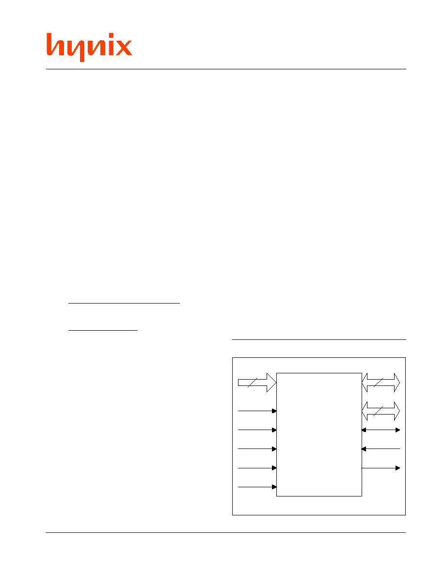
A[19:0]
20
C E #
O E #
R E S E T #
B Y T E #
W E #
8
7
DQ[7:0]
DQ[14:8]
DQ[15]/A[-1]
R Y / B Y #
W P # / A C C
LOGIC DIAGRAM
n
Data# Polling and Toggle Bits
-
Provide software confirmation of completion
of program or erase operations
n
Ready/Busy# Pin
-
Provides hardware confirmation of
completion of program or erase operations
n
Erase Suspend
-
Suspends an erase operation to allow
programming data to or reading data from
a sector in the same bank
-
Erase Resume can then be invoked to
complete the suspended erasure
n
Hardware Reset Pin (RESET#) Resets the
Device to Reading Array Data
n
WP#/ACC Input Pin
-
Write protect (WP#) function allows
hardware protection of two outermost boot
sectors, regardless of sector protect status
-
Acceleration (ACC) function provides
accelerated program times
n
Fast Program and Erase Times
-
Sector erase time: 1 sec typical
-
Byte/Word program time utilizing
Acceleration function: 13 µs typical
n
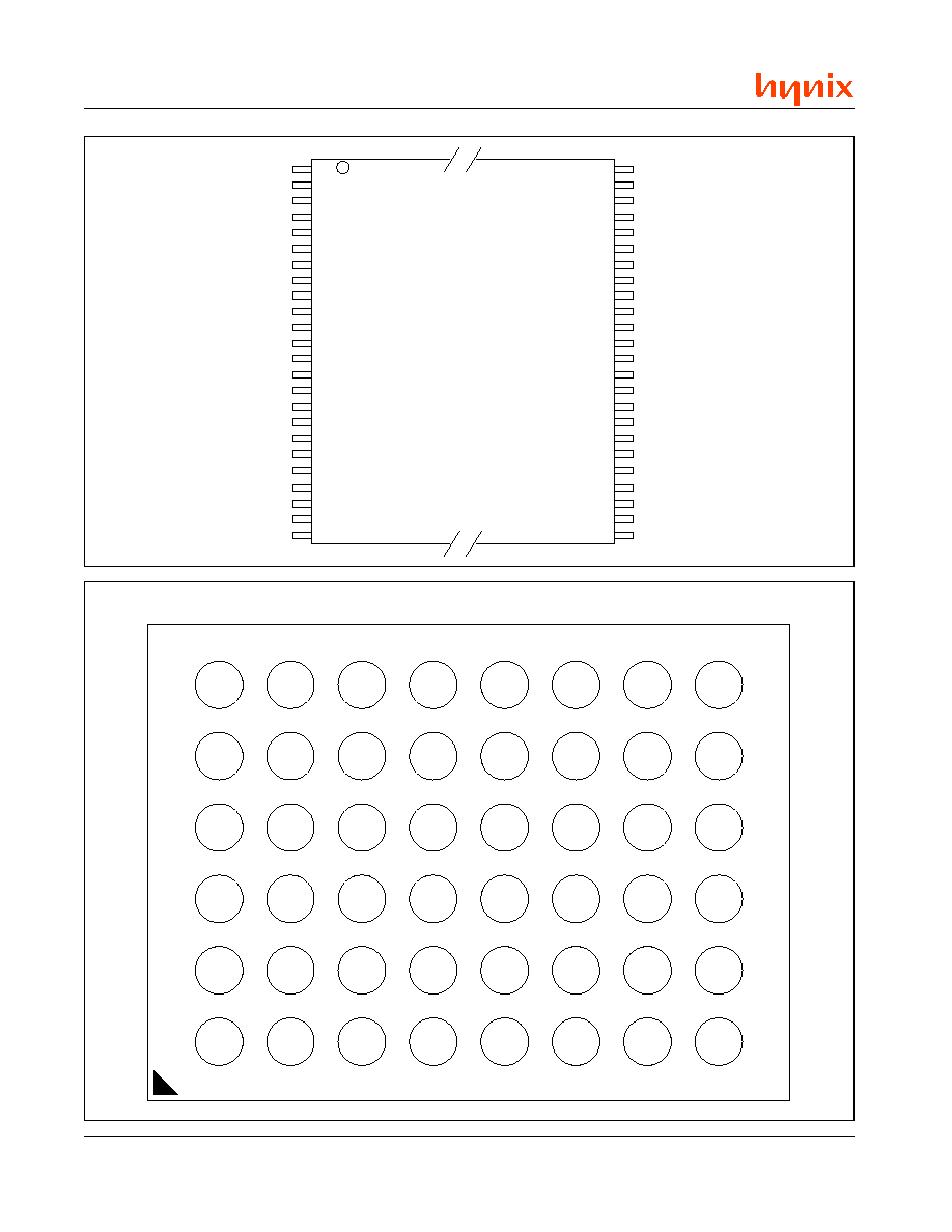
Space Efficient Packaging
-
48-pin TSOP and 48-ball FBGA packages
HY29DS162/HY29DS163
16 Megabit (2M x 8/1M x 16) Super-Low Voltage,
Dual Bank, Simultaneous Read/Write, Flash Memory
2
HY29DS162/HY29DS163
r1.3/Apr 01
GENERAL DESCRIPTION
The HY29DS162/HY29DS163 (HY29DS16x) is a
16 Mbit, 1.8 volt-only CMOS Flash memory orga-
nized as 2,097,152 (2M) bytes or 1,048,576 (1M)
words. The device is available in 48-pin TSOP
and 48-ball FBGA packages. Word-wide data
(x16) appears on DQ[15:0] and byte-wide (x8) data
appears on DQ[7:0].
The HY29DS16x Flash memory array is organized
into 39 sectors in two banks. Bank 1 contains
eight 8 Kbyte boot/parameter sectors and 3 or 7
larger sectors of 64 Kbytes each, depending on
the version of the device. Bank 2 contains the
rest of the memory array, organized as 28 or 24
sectors of 64 Kbytes:
The device features simultaneous read/write op-
eration which allows the host system to invoke a
program or erase operation in one bank and im-
mediately and simultaneously read data from the
other bank, except if that bank has any sectors
marked for erasure, with zero latency. This re-
leases the system from waiting for the completion
of program or erase operations, thus improving
overall system performance.
The HY29DS16x can be programmed and erased
in-system with a single 2.0 volt ± 10% V
CC
supply.
Internally generated and regulated voltages are
provided for program and erase operations, so that
the device does not require a higher voltage V
PP
power supply to perform those functions. The de-
vice can also be programmed in standard EPROM
programmers. Access times as low as 120 ns are
offered for timing compatibility with the zero wait
state requirements of high speed microproces-
sors. To eliminate bus contention, the HY29DS16x
has separate chip enable (CE#), write enable
(WE#) and output enable (OE#) controls.
The device is compatible with the JEDEC single-
power-supply Flash command set standard. Com-
mands are written to the command register using
standard microprocessor write timings, from where
they are routed to an internal state-machine that
controls the erase and programming circuits.
Device programming is performed a byte/word at
a time by executing the four-cycle Program Com-
mand write sequence. This initiates an internal
algorithm that automatically times the program
pulse widths and verifies proper cell margin. Faster
programming times can be achieved by placing
the HY29DS16x in the Unlock Bypass mode, which
requires only two write cycles to program data in-
stead of four.
The HY29DS16x's sector erase architecture al-
lows any number of array sectors, in one or both
banks, to be erased and reprogrammed without
affecting the data contents of other sectors. De-
vice erasure is initiated by executing the Erase
Command sequence. This initiates an internal al-
gorithm that automatically preprograms the sec-
tor before executing the erase operation. As dur-
ing programming cycles, the device automatically
times the erase pulse widths and verifies proper
cell margin. Hardware Sector Group Protection
optionally disables both program and erase op-
erations in any combination of the sector groups,
while Temporary Sector Group Unprotect, which
requires a high voltage on one pin, allows in-sys-
tem erasure and code changes in previously pro-
tected sector groups. Erase Suspend enables the
user to put erase on hold in a bank for any period
of time to read data from or program data to any
sector in that bank that is not selected for era-
sure. True background erase can thus be
achieved. Because the HY29DS16x features si-
multaneous read/write capability, there is no need
to suspend to read from a sector located within a
bank that does not contain sectors marked for era-
sure. The device is fully erased when shipped
from the factory.
Addresses and data needed for the programming
and erase operations are internally latched during
write cycles. The host system can detect comple-
tion of a program or erase operation by observing
the RY/BY# pin or by reading the DQ[7] (Data#
Polling) and DQ[6] (Toggle) status bits. Hardware
data protection measures include a low V
CC
de-
tector that automatically inhibits write operations
during power transitions.
After a program or erase cycle has been com-
pleted, or after assertion of the RESET# pin (which
terminates any operation in progress), the device
is ready to read data or to accept another com-
1
k
n
a
B
2
k
n
a
B
2
6
1
S
D
9
2
Y
H
W
K
4
/
B
K
8
x
8
W
K
2
3
/
B
K
4
6
x
3
W
K
2
3
/
B
K
4
6
x
8
2
3
6
1
S
D
9
2
Y
H
W
K
4
/
B
K
8
x
8
W
K
2
3
/
B
K
4
6
x
7
W
K
2
3
/
B
K
4
6
x
4
2
3
HY29DS162/HY29DS163
r1.3/Apr 01
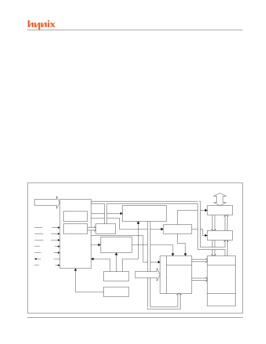
BLOCK DIAGRAM
STATE
CONTROL
W E #
C E #
R E S E T #
B Y T E #
C O M M A N D
R E G I S T E R
A[19:0], A[-1]
V
C C
D E T E C T O R
T I M E R
E R A S E V O L T A G E
G E N E R A T O R A N D
S E C T O R S W I T C H E S
P R O G R A M
V O L T A G E
G E N E R A T O R
ADDRESS LATCH
X - D E C O D E R
Y - D E C O D E R
16 Mb FLASH
M E M O R Y
A R R A Y
(2 Banks,
39 Sectors)
0.5 Mb FLASH
Security Sector
Y - G A T I N G
D A T A L A T C H
I/O BUFFERS
I/O CONTROL
RY/BY#
DQ[15:0]
CFI
C O N T R O L
CFI DATA
M E M O R Y
A[19:0], A[-1]
W P # / A C C
O E #
mand. Reading data out of the device is similar to
reading from other Flash or EPROM devices.
The Secured Sector is an extra 64 KByte sector
capable of being permanently locked at the fac-
tory or by customers. The Secured Indicator Bit
(accessed via the Electronic ID mode) is perma-
nently set to a 1 if the part is factory locked, and
permanently set to a 0 if customer lockable. This
way, customer lockable parts can never be used
to replace a factory locked part. Factory locked
parts provide several options. The Secured Sec-
tor may store a secure, random 16-byte ESN (Elec-
tronic Serial Number), customer code programmed
at the factory, or both. Customer Lockable parts
may utilize the Secured Sector as bonus space,
reading and writing like any other Flash sector, or
may permanently lock their own code there.
The WP#/ACC pin provides access to two func-
tions. The Write Protect function provides a hard-
ware method of protecting certain boot sectors
without using a high voltage. The Accelerate func-
tion speeds up programming operations, and is
intended primarily to allow faster manufacturing
throughput.
Two power-saving features are embodied in the
HY29DS16x. When addresses have been stable
for a specified amount of time, the device enters
the automatic sleep mode. The host can also place
the device into the standby mode. Power con-
sumption is greatly reduced in both these modes.
Common Flash Memory Interface (CFI)
To make Flash memories interchangeable and to
encourage adoption of new Flash technologies,
major Flash memory suppliers developed a flex-
ible method of identifying Flash memory sizes and
configurations in which all necessary Flash device
parameters are stored directly on the device.
Parameters stored include memory size, byte/word
configuration, sector configuration, necessary volt-
ages and timing information. This allows one set
of software drivers to identify and use a variety of
different, current and future Flash products. The
standard which details the software interface nec-
essary to access the device to identify it and to
determine its characteristics is the Common Flash
Memory Interface (CFI) Specification. The
HY29DS16x is fully compliant with this specification.