HY29F800_DS
KEY FEATURES
5 Volt Read, Program, and Erase
Minimizes system-level power requirements
High Performance
Access times as fast as 50 ns
Low Power Consumption
20 mA typical active read current in byte
mode, 28 mA typical in word mode
30 mA typical program/erase current
5 µA maximum CMOS standby current
Compatible with JEDEC Standards
Package, pinout and command-set
compatible with the single-supply Flash
device standard
Provides superior inadvertent write
protection
Sector Erase Architecture
Boot sector architecture with top and
bottom boot block options available
One 16 Kbyte, two 8 Kbyte, one 32 Kbyte
and seven 64 Kbyte sectors in byte mode
One 8 Kword, two 4 Kword, one 16 Kword
and seven 32 Kword sectors in word mode
A command can erase any combination of
sectors
Supports full chip erase
Erase Suspend/Resume
Temporarily suspends a sector erase
operation to allow data to be read from, or
programmed into, any sector not being
erased
Sector Protection
Any combination of sectors may be locked
to prevent program or erase operations
within those sectors
Temporary Sector Unprotect
Allows changes in locked sectors
(requires high voltage on RESET# pin)
Internal Erase Algorithm
Automatically erases a sector, any
combination of sectors, or the entire chip
Internal Programming Algorithm
Automatically programs and verifies data
at a specified address
Fast Program and Erase Times
Byte programming time: 7 µs typical
Sector erase time: 1.0 sec typical
Chip erase time: 11 sec typical
Data# Polling and Toggle Status Bits
Provide software confirmation of
completion of program or erase
operations
Ready/Busy# Output (RY/BY#)
Provides hardware confirmation of
completion of program and erase
operations
100,000 Program/Erase Cycles Minimum
Space Efficient Packaging
Available in industry-standard 44-pin
PSOP and 48-pin TSOP and reverse
TSOP packages
Preliminary
Revision 1.0, January 2002
GENERAL DESCRIPTION
The HY29F400A is a 4 Megabit, 5 volt only CMOS
Flash memory organized as 524,288 (512K) bytes
or 262,144 (256K) words. The device is offered in
industry-standard 44-pin PSOP and 48-pin TSOP
packages.
The HY29F400A can be programmed and erased
in-system with a single 5-volt V
CC
supply. Internally
generated and regulated voltages are provided for
program and erase operations, so that the device
does not require a high voltage power supply to
perform those functions. The device can also be
programmed in standard EPROM programmers.
Access times as fast as 55 ns over the full operat-
ing voltage range of 5.0 volts ± 10% are offered
for timing compatibility with the zero wait state re-
quirements of high speed microprocessors. A 55
ns version operating over 5.0 volts ± 5% is also
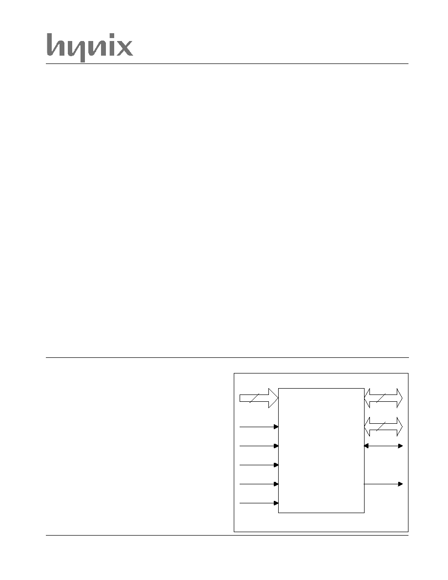
A[17:0]
18
CE#
OE#
RESET#
BYTE#
WE#
8
7
DQ[7:0]
DQ[14:8]
DQ[15]/A-1
RY/BY#
LOGIC DIAGRAM
HY29F400A
4 Megabit (512Kx8/256Kx16) 5 Volt-only Flash Memory
2
Rev. 1.0/Jan. 02
HY29F400A
available. To eliminate bus contention, the
HY29F400A has separate chip enable (CE#), write
enable (WE#) and output enable (OE#) controls.
The device is compatible with the JEDEC single
power-supply Flash command set standard. Com-
mands are written to the command register using
standard microprocessor write timings, from where
they are routed to an internal state-machine that
controls the erase and programming circuits. De-
vice programming is performed a byte or word at
a time by executing the four-cycle Program com-
mand. This initiates an internal algorithm that au-
tomatically times the program pulse widths and
verifies proper cell margin.
The HY29F400A's sector erase architecture allows
any number of array sectors to be erased and re-
programmed without affecting the data contents
of other sectors. Device erasure is initiated by ex-
ecuting the Erase command. This initiates an in-
ternal algorithm that automatically preprograms the
array (if it is not already programmed) before ex-
ecuting the erase operation. During erase cycles,
the device automatically times the erase pulse
widths and verifies proper cell margin.
To protect data in the device from accidental or
unauthorized attempts to program or erase the
device while it is in the system (e.g., by a virus),
the device has a Sector Protect function which
hardware write protects selected sectors. The
sector protect and unprotect features can be en-
abled in a PROM programmer. Temporary Sector
Unprotect, which requires a high voltage, allows
in-system erasure and code changes in previously
protected sectors.
Erase Suspend enables the user to put erase on
hold for any period of time to read data from, or
program data to, any sector that is not selected
for erasure. True background erase can thus be
achieved. The device is fully erased when shipped
from the factory.
Addresses and data needed for the programming
and erase operations are internally latched during
write cycles, and the host system can detect
completion of a program or erase operation by
observing the RY/BY# pin, or by reading the DQ[7]
(Data# Polling) and DQ[6] (Toggle) status bits.
Reading data from the device is similar to reading
from SRAM or EPROM devices. Hardware data
protection measures include a low V
CC
detector
that automatically inhibits write operations during
power transitions.
The host can place the device into the standby
mode. Power consumption is greatly reduced in
this mode.
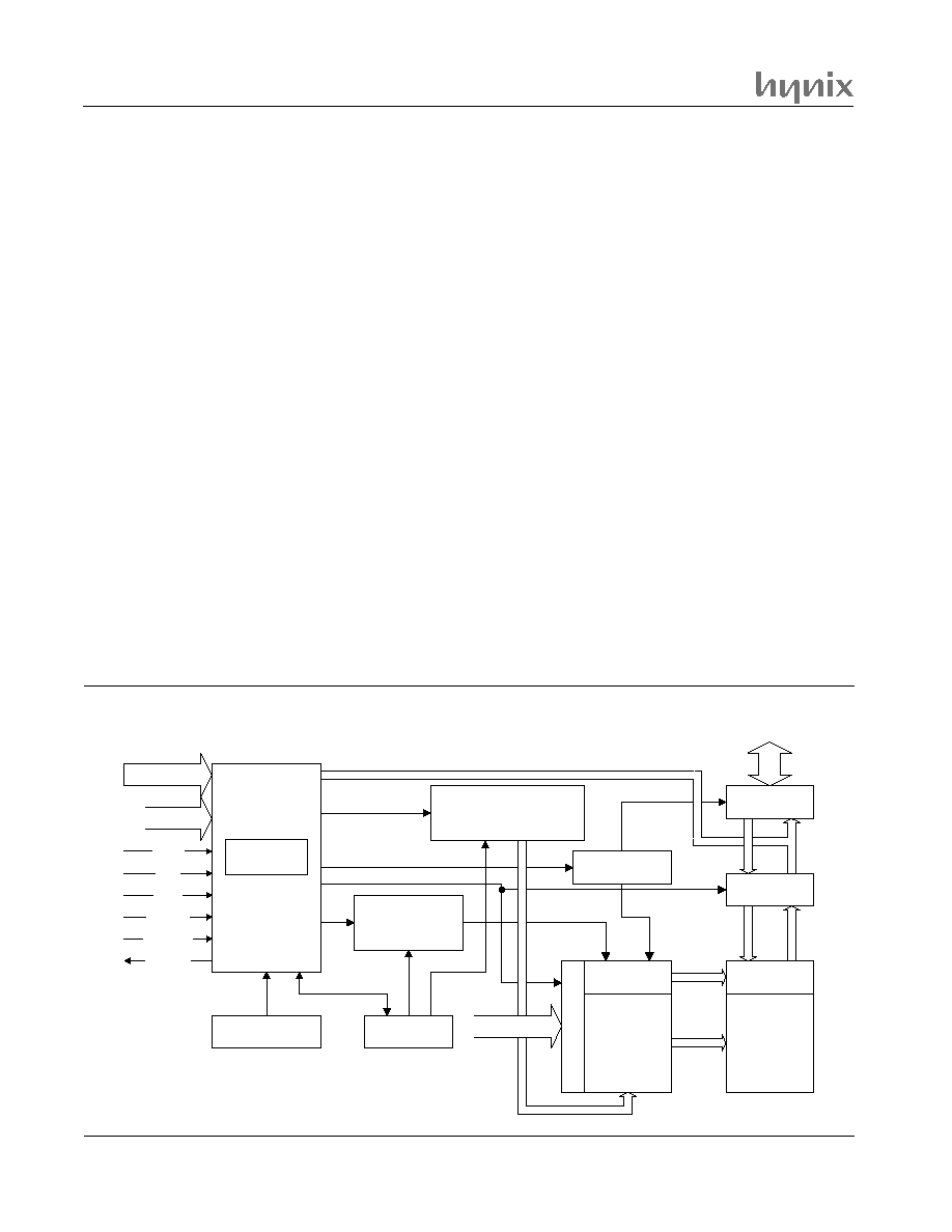
BLOCK DIAGRAM
STATE
CONTROL
WE#
CE#
OE#
BYTE#
COMMAND
REGISTER
DQ[15:0]
A[17:0], A-1
V
CC
DETECTOR
TIMER
ERASE VOLTAGE
GENERATOR AND
SECTOR SWITCHES
PROGRAM
VOLTAGE
GENERATOR
AD
D
R
ESS L
A
T
C
H
X-DECODER
Y-DECODER
4 Mb FLASH
MEMORY
ARRAY
Y-GATING
DATA LATCH
I/O BUFFERS
I/O CONTROL
RESET#
DQ[15:0]
A[17:0], A-1
RY/BY#
3
Rev. 1.0/Jan. 02
HY29F400A
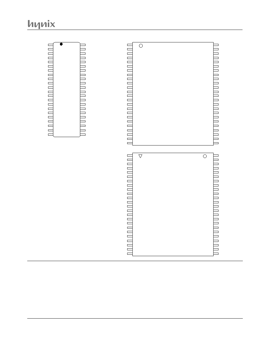
PIN CONFIGURATIONS
Standard
TSOP48
DQ7
DQ14
44
43
DQ6
DQ13
42
41
DQ5
DQ12
40
39
DQ4
V
CC
38
37
DQ11
DQ3
36
35
DQ10
DQ2
34
33
DQ9
DQ1
32
31
DQ8
DQ0
30
29
A16
BYTE#
48
47
V
SS
DQ15/A-1
46
45
OE#
V
SS
28
27
CE#
A0
26
25
A11
A10
5
6
A9
A8
7
8
NC
NC
9
10
WE#
RESET#
11
12
NC
NC
13
14
RY/BY#
NC
15
16
A17
A7
17
18
A6
A5
19
20
A15
A14
1
2
A13
A12
3
4
A4
A3
21
22
A2
A1
23
24
Reverse
TSOP48
44
43
42
41
40
39
38
37
36
35
34
33
32
31
30
29
48
47
46
45
28
27
26
25
5
6
7
8
9
10
11
12
13
14
15
16
17
18
19
20
1
2
3
4
21
22
23
24
A11
A10
A9
A8
NC
NC
WE#
RESET#
NC
NC
RY/BY#
NC
A17
A7
A6
A5
A15
A14
A13
A12
A4
A3
A2
A1
DQ7
DQ14
DQ6
DQ13
DQ5
DQ12
DQ4
V
CC
DQ11
DQ3
DQ10
DQ2
DQ9
DQ1
DQ8
DQ0
A16
BYTE#
V
SS
DQ15/A-1
OE#
V
SS
CE#
A0
A6
A5
5
6
A4
A3
7
8
A2
A1
9
10
A0
CE#
11
12
V
SS
OE#
13
14
DQ0
DQ8
15
16
DQ1
DQ9
17
18
DQ2
DQ10
19
20
DQ3
DQ11
21
22
NC
RY/BY#
1
2
A17
A7
3
4
A10
A11
40
39
A12
A13
38
37
A14
A15
36
35
A16
BYTE#
34
33
V
SS
DQ15/A-1
32
31
DQ7
DQ14
30
29
DQ6
DQ13
28
27
DQ5
DQ12
26
25
DQ4
V
CC
24
23
RESET#
WE#
44
43
A8
A9
42
41
PSOP44
CONVENTIONS
Unless otherwise noted, a positive logic (active
High) convention is assumed throughout this docu-
ment, whereby the presence at a pin of a higher,
more positive voltage (nominally 5VDC) causes
assertion of the signal. A `#' symbol following the
signal name, e.g., RESET#, indicates that the sig-
nal is asserted in a Low state (nominally 0 volts).
Whenever a signal is separated into numbered
bits, e.g., DQ[7], DQ[6], ..., DQ[0], the family of
bits may also be shown collectively, e.g., as
DQ[7:0].
The designation 0xNNNN (N = 0, 1, 2, . . . , 9, A, . . .
, E, F) indicates a number expressed in hexadeci-
mal notation. The designation 0bXXXX indicates a
number expressed in binary notation (X = 0, 1).
4
Rev. 1.0/Jan. 02
HY29F400A
SIGNAL DESCRIPTIONS
e
m
a
N
e
p
y
T
n
o
i
t
p
i
r
c
s
e
D
]
0
:
7
1
[
A
s
t
u
p
n
I
.
h
g
i
H
e
v
i
t
c
a
,
s
s
e
r
d
d
A
4
4
1
,
2
6
2
f
o
e
n
o
t
c
e
l
e
s
s
t
u
p
n
i
8
1
e
s
e
h
t
,
e
d
o
m
d
r
o
W
n
I
e
s
e
h
t
,
e
d
o
m
e
t
y
B
n
I
.
s
n
o
i
t
a
r
e
p
o
e
t
i
r
w
r
o
d
a
e
r
r
o
f
y
a
r
r
a
e
h
t
n
i
h
t
i
w
s
d
r
o
w
)
K
6
5
2
(
8
8
2
,
4
2
5
f
o
e
n
o
t
c
e
l
e
s
o
t
)
B
S
L
(
t
u
p
n
i
1
-
A
/
5
1
Q
D
e
h
t
h
t
i
w
d
e
n
i
b
m
o
c
e
r
a
s
t
u
p
n
i
.
s
n
o
i
t
a
r
e
p
o
e
t
i
r
w
r
o
d
a
e
r
r
o
f
y
a
r
r
a
e
h
t
n
i
h
t
i
w
s
e
t
y
b
)
K
2
1
5
(
,
]
1
-
[
A
/
]
5
1
[
Q
D
]
0
:
4
1
[
Q
D
s
t
u
p
t
u
O
/
s
t
u
p
n
I
e
t
a
t
s
-
i
r
T
h
g
i
H
e
v
i
t
c
a
,
s
u
B
a
t
a
D
h
t
a
p
a
t
a
d
t
i
b
-
6
1
a
e
d
i
v
o
r
p
s
n
i
p
e
s
e
h
t
,
e
d
o
m
d
r
o
W
n
I
.
h
t
a
p
a
t
a
d
t
i
b
-
8
n
a
e
d
i
v
o
r
p
]
0
:
7
[
Q
D
,
e
d
o
m
e
t
y
B
n
I
.
s
n
o
i
t
a
r
e
p
o
e
t
i
r
w
d
n
a
d
a
e
r
r
o
f
]
8
:
4
1
[
Q
D
.
t
u
p
n
i
s
s
e
r
d
d
a
e
t
y
b
t
i
b
-
9
1
e
h
t
f
o
B
S
L
e
h
t
s
a
d
e
s
u
s
i
]
1
-
[
A
/
]
5
1
[
Q
D
d
n
a
.
e
d
o
m
e
t
y
B
n
i
d
e
t
a
t
s
-
i
r
t
n
i
a
m
e
r
d
n
a
d
e
s
u
n
u
e
r
a
#
E
T
Y
B
t
u
p
n
I
.
w
o
L
e
v
i
t
c
a
,
e
d
o
M
e
t
y
B
.
e
c
i
v
e
d
e
h
t
f
o
n
o
i
t
a
r
u
g
i
f
n
o
c
d
r
o
W
/
e
t
y
B
e
h
t
s
l
o
r
t
n
o
C
.
e
d
o
m
d
r
o
W
s
t
c
e
l
e
s
h
g
i
H
,
e
d
o
m
e
t
y
B
s
t
c
e
l
e
s
w
o
L
#
E
C
t
u
p
n
I
.
w
o
L
e
v
i
t
c
a
,
e
l
b
a
n
E
p
i
h
C
r
o
m
o
r
f
a
t
a
d
d
a
e
r
o
t
d
e
t
r
e
s
s
a
e
b
t
s
u
m
t
u
p
n
i
s
i
h
T
e
h
t
d
n
a
d
e
t
a
t
s
-
i
r
t
s
i
s
u
b
a
t
a
d
e
h
t
,
h
g
i
H
n
e
h
W
.
A
0
0
4
F
9
2
Y
H
e
h
t
o
t
a
t
a
d
e
t
i
r
w
.
e
d
o
m
y
b
d
n
a
t
S
e
h
t
n
i
d
e
c
a
l
p
s
i
e
c
i
v
e
d
#
E
O
t
u
p
n
I
w
o
L
e
v
i
t
c
a
,
e
l
b
a
n
E
t
u
p
t
u
O
s
n
o
i
t
a
r
e
p
o
d
a
e
r
r
o
f
d
e
t
r
e
s
s
a
e
b
t
s
u
m
t
u
p
n
i
s
i
h
T
.
d
r
o
w
a
r
o
e
t
y
b
a
r
e
h
t
e
h
w
s
e
n
i
m
r
e
t
e
d
#
E
T
Y
B
.
s
n
o
i
t
a
r
e
p
o
e
t
i
r
w
r
o
f
d
e
t
a
g
e
n
d
n
a
e
r
a
e
c
i
v
e
d
e
h
t
m
o
r
f
s
t
u
p
t
u
o
a
t
a
d
,
h
g
i
H
n
e
h
W
.
n
o
i
t
a
r
e
p
o
d
a
e
r
e
h
t
g
n
i
r
u
d
d
a
e
r
s
i
.
e
t
a
t
s
e
c
n
a
d
e
p
m
i
h
g
i
h
e
h
t
n
i
d
e
c
a
l
p
e
r
a
s
n
i
p
s
u
b
a
t
a
d
e
h
t
d
n
a
d
e
l
b
a
s
i
d
#
E
W
t
u
p
n
I
.
w
o
L
e
v
i
t
c
a
,
e
l
b
a
n
E
e
t
i
r
W
d
n
a
m
m
o
c
r
o
s
d
n
a
m
m
o
c
f
o
g
n
i
t
i
r
w
s
l
o
r
t
n
o
C
A
.
y
a
r
r
a
y
r
o
m
e
m
e
h
t
f
o
s
r
o
t
c
e
s
e
s
a
r
e
r
o
a
t
a
d
m
a
r
g
o
r
p
o
t
r
e
d
r
o
n
i
s
e
c
n
e
u
q
e
s
#
E
O
d
n
a
w
o
L
s
i
#
E
C
e
l
i
h
w
d
e
t
r
e
s
s
a
s
i
#
E
W
n
e
h
w
e
c
a
l
p
s
e
k
a
t
n
o
i
t
a
r
e
p
o
e
t
i
r
w
e
t
i
r
w
e
h
t
g
n
i
r
u
d
n
e
t
t
i
r
w
s
i
d
r
o
w
a
r
o
e
t
y
b
a
r
e
h
t
e
h
w
s
e
n
i
m
r
e
t
e
d
#
E
T
Y
B
.
h
g
i
H
s
i
.
n
o
i
t
a
r
e
p
o
#
T
E
S
E
R
t
u
p
n
I
.
w
o
L
e
v
i
t
c
a
,
t
e
s
e
R
e
r
a
w
d
r
a
H
e
h
t
g
n
i
t
t
e
s
e
r
f
o
d
o
h
t
e
m
e
r
a
w
d
r
a
h
a
s
e
d
i
v
o
r
P
y
l
e
t
a
i
d
e
m
m
i
t
i
,
t
e
s
e
r
s
i
e
c
i
v
e
d
e
h
t
n
e
h
W
.
e
t
a
t
s
y
a
r
r
a
d
a
e
r
e
h
t
o
t
A
0
0
4
F
9
2
Y
H
e
t
i
r
w
/
d
a
e
r
ll
a
d
n
a
d
e
t
a
t
s
-
i
r
t
s
i
s
u
b
a
t
a
d
e
h
T
.
s
s
e
r
g
o
r
p
n
i
n
o
i
t
a
r
e
p
o
y
n
a
s
e
t
a
n
i
m
r
e
t
,
d
e
t
r
e
s
s
a
s
i
#
T
E
S
E
R
e
l
i
h
W
.
d
e
t
r
e
s
s
a
s
i
t
u
p
n
i
e
h
t
e
l
i
h
w
d
e
r
o
n
g
i
e
r
a
s
d
n
a
m
m
o
c
.
e
d
o
m
y
b
d
n
a
t
S
e
h
t
n
i
e
b
ll
i
w
e
c
i
v
e
d
e
h
t
#
Y
B
/
Y
R
t
u
p
t
u
O
n
i
a
r
D
n
e
p
O
.
s
u
t
a
t
S
y
s
u
B
/
y
d
a
e
R
n
i
s
i
d
n
a
m
m
o
c
e
s
a
r
e
r
o
e
t
i
r
w
a
r
e
h
t
e
h
w
s
e
t
a
c
i
d
n
I
e
h
t
f
o
e
g
d
e
g
n
i
s
i
r
e
h
t
r
e
t
f
a
d
il
a
v
s
i
#
Y
B
/
Y
R
.
d
e
t
e
l
p
m
o
c
n
e
e
b
s
a
h
r
o
s
s
e
r
g
o
r
p
s
i
e
c
i
v
e
d
e
h
t
e
l
i
h
w
w
o
L
s
n
i
a
m
e
r
t
I
.
e
c
n
e
u
q
e
s
d
n
a
m
m
o
c
a
f
o
e
s
l
u
p
#
E
W
l
a
n
i
f
d
a
e
r
o
t
y
d
a
e
r
s
i
t
i
n
e
h
w
h
g
i
H
s
e
o
g
d
n
a
,
g
n
i
s
a
r
e
r
o
a
t
a
d
g
n
i
m
m
a
r
g
o
r
p
y
l
e
v
i
t
c
a
.
a
t
a
d
y
a
r
r
a
V
C
C
-
-
.
y
l
p
p
u
s
r
e
w
o
p
)
l
a
n
i
m
o
n
(
t
l
o
v
-
5
V
S
S
-
-
.
d
n
u
o
r
g
l
a
n
g
i
s
d
n
a
r
e
w
o
P
5
Rev. 1.0/Jan. 02
HY29F400A
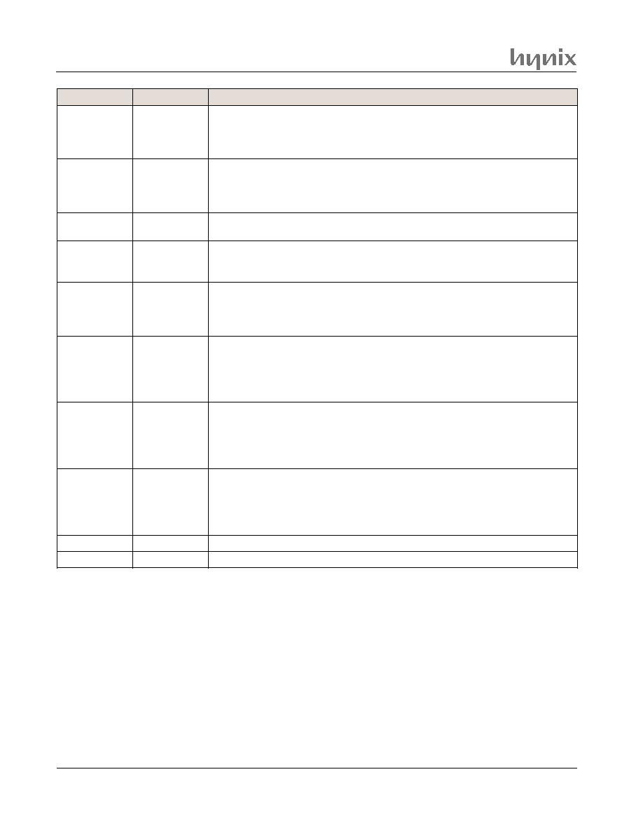
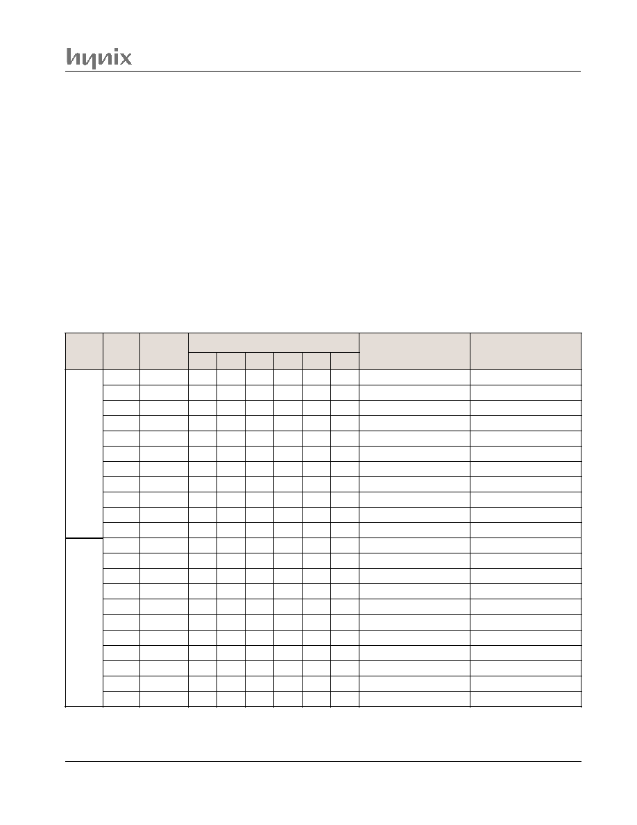
MEMORY ARRAY ORGANIZATION
The 4 Mbit Flash memory array is organized into
11 blocks called sectors (S0, S1, . . . , S10). A
sector is the smallest unit that can be erased and
which can be protected to prevent accidental or
unauthorized erasure. See the `Bus Operations'
and `Command Definitions' sections of this docu-
ment for additional information on these functions.
In the HY29F400A, four of the sectors, which com-
prise the boot block, vary in size from 8 to 32
Kbytes (4 to 16 Kwords), while the remaining
seven sectors are uniformly sized at 64 Kbytes
(32 Kwords). The boot block can be located at
the bottom of the address range (HY29F400AB)
or at the top of the address range (HY29F400AT).
Table 1. HY29F400A Memory Array Organization
Notes:
1. X indicates Don't Care.
2. Address in Byte Mode is A[17:-1].
3. Address in Word Mode is A[17:0].
BUS OPERATIONS
Device bus operations are initiated through the
internal command register, which consists of sets
of latches that store the commands, along with
the address and data information, if any, needed
to execute the specific command. The command
register itself does not occupy any addressable
memory location. The contents of the command
register serve as inputs to an internal state ma-
chine whose outputs control the operation of the
device. Table 2 lists the normal bus operations,
HY29F400A
T - T
op Boot Block
HY29F400AB - Bottom Boot Block
e
c
i
v
e
D
r
o
t
c
e
S
e
z
i
S
)
W
K
/
B
K
(
s
s
e
r
d
d
A
r
o
t
c
e
S
e
d
o
M
e
t
y
B
e
g
n
a
R
s
s
e
r
d
d
A
2
e
d
o
M
d
r
o
W
e
g
n
a
R
s
s
e
r
d
d
A
3
]
7
1
[
A
]
6
1
[
A
]
5
1
[
A
]
4
1
[
A
]
3
1
[
A
]
2
1
[
A
0
S
2
3
/
4
6
0
0
0
X
X
X
F
F
F
F
0
x
0
-
0
0
0
0
0
x
0
F
F
F
7
0
x
0
-
0
0
0
0
0
x
0
1
S
2
3
/
4
6
0
0
1
X
X
X
F
F
F
F
1
x
0
-
0
0
0
0
1
x
0
F
F
F
F
0
x
0
-
0
0
0
8
0
x
0
2
S
2
3
/
4
6
0
1
0
X
X
X
F
F
F
F
2
x
0
-
0
0
0
0
2
x
0
F
F
F
7
1
x
0
-
0
0
0
0
1
x
0
3
S
2
3
/
4
6
0
1
1
X
X
X
F
F
F
F
3
x
0
-
0
0
0
0
3
x
0
F
F
F
F
1
x
0
-
0
0
0
8
1
x
0
4
S
2
3
/
4
6
1
0
0
X
X
X
F
F
F
F
4
x
0
-
0
0
0
0
4
x
0
F
F
F
7
2
x
0
-
0
0
0
0
2
x
0
5
S
2
3
/
4
6
1
0
1
X
X
X
F
F
F
F
5
x
0
-
0
0
0
0
5
x
0
F
F
F
F
2
x
0
-
0
0
0
8
2
x
0
6
S
2
3
/
4
6
1
1
0
X
X
X
F
F
F
F
6
x
0
-
0
0
0
0
6
x
0
F
F
F
7
3
x
0
-
0
0
0
0
3
x
0
7
S
6
1
/
2
3
1
1
1
0
X
X
F
F
F
7
7
x
0
-
0
0
0
0
7
x
0
F
F
F
B
3
x
0
-
0
0
0
8
3
x
0
8
S
4
/
8
1
1
1
1
0
0
F
F
F
9
7
x
0
-
0
0
0
8
7
x
0
F
F
F
C
3
x
0
-
0
0
0
C
3
x
0
9
S
4
/
8
1
1
1
1
0
1
F
F
F
B
7
x
0
-
0
0
0
A
7
x
0
F
F
F
D
3
x
0
-
0
0
0
D
3
x
0
0
1
S
8
/
6
1
1
1
1
1
1
X
F
F
F
F
7
x
0
-
0
0
0
C
7
x
0
F
F
F
F
3
x
0
-
0
0
0
E
3
x
0
0
S
8
/
6
1
0
0
0
0
0
X
F
F
F
3
0
x
0
-
0
0
0
0
0
x
0
F
F
F
1
0
x
0
-
0
0
0
0
0
x
0
1
S
4
/
8
0
0
0
0
1
0
F
F
F
5
0
x
0
-
0
0
0
4
0
x
0
F
F
F
2
0
x
0
-
0
0
0
2
0
x
0
2
S
4
/
8
0
0
0
0
1
1
F
F
F
7
0
x
0
-
0
0
0
6
0
x
0
F
F
F
3
0
x
0
-
0
0
0
3
0
x
0
3
S
6
1
/
2
3
0
0
0
1
X
X
F
F
F
F
0
x
0
-
0
0
0
8
0
x
0
F
F
F
7
0
x
0
-
0
0
0
4
0
x
0
4
S
2
3
/
4
6
0
0
1
X
X
X
F
F
F
F
1
x
0
-
0
0
0
0
1
x
0
F
F
F
F
0
x
0
-
0
0
0
8
0
x
0
5
S
2
3
/
4
6
0
1
0
X
X
X
F
F
F
F
2
x
0
-
0
0
0
0
2
x
0
F
F
F
7
1
x
0
-
0
0
0
0
1
x
0
6
S
2
3
/
4
6
0
1
1
X
X
X
F
F
F
F
3
x
0
-
0
0
0
0
3
x
0
F
F
F
F
1
x
0
-
0
0
0
8
1
x
0
7
S
2
3
/
4
6
1
0
0
X
X
X
F
F
F
F
4
x
0
-
0
0
0
0
4
x
0
F
F
F
7
2
x
0
-
0
0
0
0
2
x
0
8
S
2
3
/
4
6
1
0
1
X
X
X
F
F
F
F
5
x
0
-
0
0
0
0
5
x
0
F
F
F
F
2
x
0
-
0
0
0
8
2
x
0
9
S
2
3
/
4
6
1
1
0
X
X
X
F
F
F
F
6
x
0
-
0
0
0
0
6
x
0
F
F
F
7
3
x
0
-
0
0
0
0
3
x
0
0
1
S
2
3
/
4
6
1
1
1
X
X
X
F
F
F
F
7
x
0
-
0
0
0
0
7
x
0
F
F
F
F
3
x
0
-
0
0
0
8
3
x
0
Table 1 defines the sector addresses and corre-
sponding address ranges for the top and bottom
boot block versions of the HY29F400A.