KEY FEATURES
n
Single Power Supply Operation
≠ Read, program and erase operations from
2.7 to 3.6 volts
≠ Ideal for battery-powered applications
n
High Performance
≠ 70, 80, 90 and 120 ns access time
versions
n
Ultra-low Power Consumption (Typical
Values At 5 Mhz)
≠ Automatic sleep mode current: 1 µA
≠ Standby mode current: 1 µA
≠ Read current: 9 mA
≠ Program/erase current: 20 mA
n
Flexible Sector Architecture:
≠ One 16 KB, two 8 KB, one 32 KB and
thirty-one 64 KB sectors in byte mode
≠ One 8 KW, two 4 KW, one 16 KW and
thirty-one 32 KW sectors in word mode
≠ Top or bottom boot block configurations
available
n
Sector Protection
≠ Allows locking of a sector or sectors to
prevent program or erase operations
within that sector
≠ Sectors lockable in-system or via
programming equipment
≠ Temporary Sector Unprotect allows
changes in locked sectors (requires high
voltage on RESET# pin)
n
Fast Program and Erase Times
≠ Sector erase time: 0.25 sec typical for
each sector
≠ Chip erase time: 8 sec typical
≠ Byte program time: 9
µ
s typical
n
Unlock Bypass Program Command
≠ Reduces programming time when issuing
multiple program command sequences
n
Automatic Erase Algorithm Preprograms
and Erases Any Combination of Sectors
or the Entire Chip
n
Erase Suspend/Erase Resume
≠ Suspends an erase operation to allow
reading data from, or programming data
to, a sector that is not being erased
≠ Erase Resume can then be invoked to
complete suspended erasure
n
Automatic Program Algorithm Writes and
Verifies Data at Specified Addresses
Preliminary
Revision 1.2, May 2001
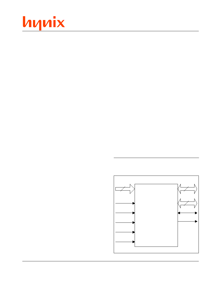
A[19:0]
2 0
C E #
O E #
R E S E T #
B Y T E #
W E #
8
7
D Q [ 7 : 0 ]
D Q [ 1 4 : 8 ]
D Q 1 5 / A - 1
R Y / B Y #
LOGIC DIAGRAM
n
100,000 Write Cycles per Sector Minimum
n
Data# Polling and Toggle Bits
≠ Provide software confirmation of
completion of program and erase
operations
n
Ready/Busy# Pin
≠ Provides hardware confirmation of
completion of program and erase
operations
n
Hardware Reset Pin (RESET#) Resets the
Device to Reading Array Data
n
Compliant With Common Flash Memory
Interface (CFI) Specification
≠ Flash device parameters stored directly
on the device
≠ Allows software driver to identify and use
a variety of different current and future
Flash products
n
Compatible With JEDEC standards
≠ Pinout and software compatible with
single-power supply Flash devices
≠ Superior inadvertent write protection
n
Space Efficient Packaging
≠ 48-pin TSOP and 48-ball FBGA packages
HY29LV160
16 Mbit (2M x 8/1M x 16) Low Voltage Flash Memory

2
Rev. 1.2/May 01
HY29LV160
GENERAL DESCRIPTION
The HY29LV160 is a 16 Mbit, 3 volt-only, CMOS
Flash memory organized as 2,097,152 (2M) bytes
or 1,048,576 (1M) words that is available in 48-
pin TSOP and 48-ball FBGA packages. Word-
wide data (x16) appears on DQ[15:0] and byte-
wide (x8) data appears on DQ[7:0].
The HY29LV160 can be programmed and erased
in-system with a single 3 volt V
CC
supply. Inter-
nally generated and regulated voltages are pro-
vided for program and erase operations, so that
the device does not require a higher voltage V
PP
power supply to perform those functions. The de-
vice can also be programmed in standard EPROM
programmers. Access times as low as 80 ns over
the full operating voltage range of 2.7 - 3.6 volts,
and 70 ns with a limited voltage range of 3.0 - 3.6
volts, are offered for timing compatibility with the
zero wait state requirements of high speed mi-
croprocessors. To eliminate bus contention, the
HY29LV160 has separate chip enable (CE#), write
enable (WE#) and output enable (OE#) controls.
The device is compatible with the JEDEC single-
power-supply Flash memory command set stan-
dard. Commands are written to the command reg-
ister using standard microprocessor write timings.
They are then routed to an internal state-machine
that controls the erase and programming circuits.
Device programming is performed a byte/word at
a time by executing the four-cycle Program Com-
mand write sequence. This initiates an internal al-
gorithm that automatically times the program pulse
widths and verifies proper cell margin. Faster pro-
gramming times can be achieved by placing the
HY29LV160 in the Unlock Bypass mode, which
requires only two write cycles to program data in-
stead of four.
The HY29LV160's sector erase architecture allows
any number of array sectors to be erased and re-
programmed without affecting the data contents
of other sectors. Device erasure is initiated by
executing the Erase Command sequence. This
initiates an internal algorithm that automatically
preprograms the array (if it is not already pro-
grammed) before executing the erase operation.
As during programming cycles, the device auto-
matically times the erase pulse widths and veri-
fies proper cell margin. Hardware Sector Protec-
tion optionally disables both program and erase
operations in any combination of the sectors of
the memory array, while Temporary Sector Un-
protect allows in-system erasure and code
changes in previously protected sectors. Erase
Suspend enables the user to put erase on hold for
any period of time to read data from, or program
data to, any sector that is not selected for era-
sure. True background erase can thus be
achieved. The device is fully erased when shipped
from the factory.
Addresses and data needed for the programming
and erase operations are internally latched during
write cycles, and the host system can detect
completion of a program or erase operation by
observing the RY/BY# pin, or by reading the DQ[7]
(Data# Polling) or DQ[6] (Toggle) status bits. Hard-
ware data protection measures include a low V
CC
detector that automatically inhibits write operations
during power transitions.
After a program or erase cycle has been com-
pleted, or after assertion of the RESET# pin (which
terminates any operation in progress), the device
is ready to read data or to accept another com-
mand. Reading data out of the device is similar to
reading from other Flash or EPROM devices.
Two power-saving features are embodied in the
HY29LV160. When addresses have been stable
for a specified amount of time, the device enters
Automatic Sleep mode. The host can also place
the device into Standby mode. Power consump-
tion is greatly reduced in both of these modes.
Common Flash Memory Interface (CFI)
To make Flash memories interchangeable and to
encourage adoption of new Flash technologies,
major Flash memory suppliers developed a flex-
ible method of identifying Flash memory sizes and
configurations in which all necessary Flash device
parameters are stored directly on the device.
Parameters stored include memory size, byte/word
configuration, sector configuration, necessary volt-
ages and timing information. This allows one set
of software drivers to identify and use a variety of
different current and future Flash products. The
standard which details the software interface nec-
essary to access the device to identify it and to
determine its characteristics is the Common Flash
Memory Interface (CFI) Specification. The
HY29LV160 is fully compliant with this specification.
3
Rev. 1.2/May 01
HY29LV160
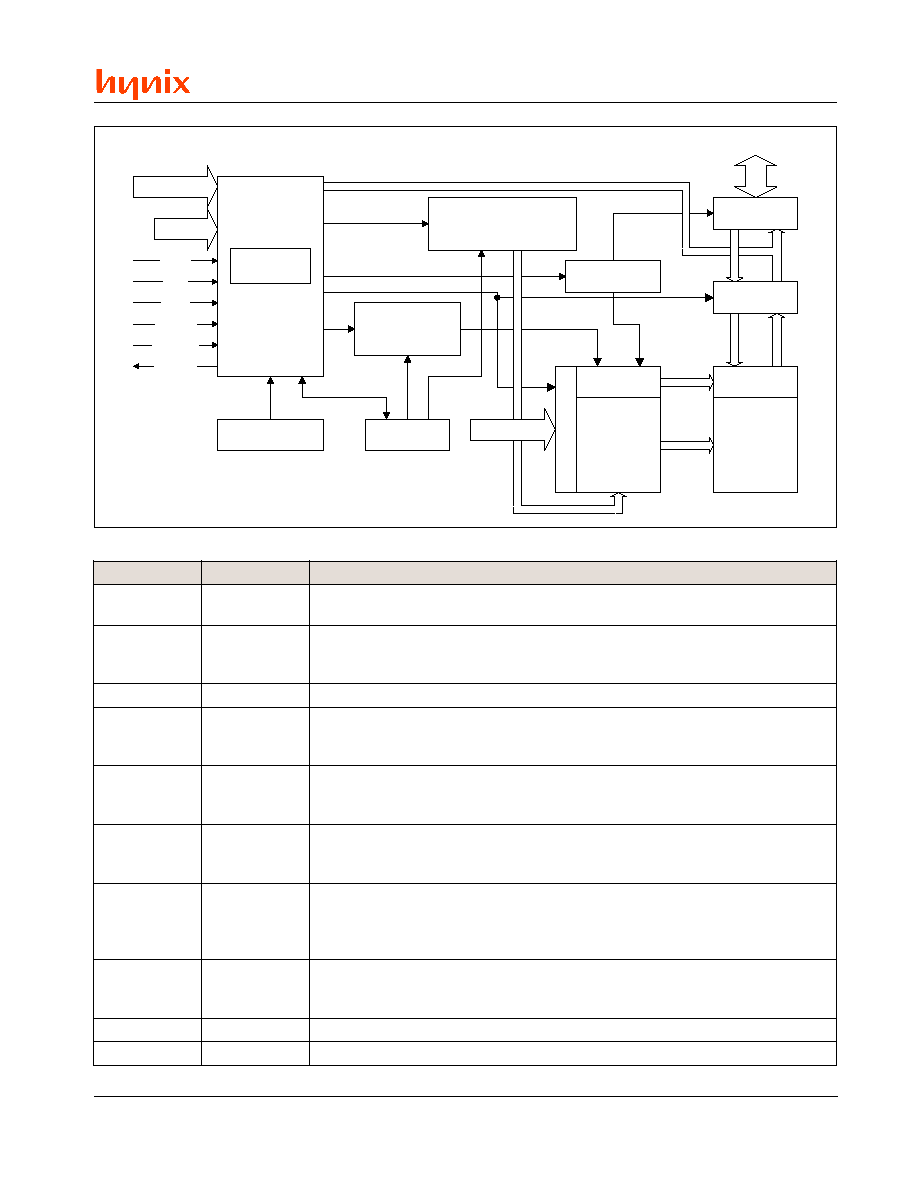
BLOCK DIAGRAM
STATE
C O N T R O L
W E #
C E #
OE#
BYTE#
C O M M A N D
R E G I S T E R
DQ[15:0]
A[19:0], A-1
V
C C
D E T E C T O R
T I M E R
E R A S E V O L T A G E
G E N E R A T O R A N D
S E C T O R S W I T C H E S
P R O G R A M
V O L T A G E
G E N E R A T O R
ADDRESS LATCH
X - D E C O D E R
Y - D E C O D E R
16 Mb FLASH
M E M O R Y
A R R A Y
Y-GATING
D A T A L A T C H
I/O BUFFERS
I/O CONTROL
R E S E T #
DQ[15:0]
A[19:0], A-1
RY/BY#
SIGNAL DESCRIPTIONS
e
m
a
N
e
p
y
T
n
o
i
t
p
i
r
c
s
e
D
]
0
:
9
1
[
A
s
t
u
p
n
I
.
h
g
i
H
e
v
i
t
c
a
,
s
s
e
r
d
d
A
n
i
t
u
p
n
i
]
1
-
[
A
/
]
5
1
[
Q
D
e
h
t
h
t
i
w
d
e
n
i
b
m
o
c
,
s
t
u
p
n
i
0
2
e
s
e
h
T
.
s
n
o
i
t
a
r
e
p
o
e
t
i
r
w
r
o
d
a
e
r
r
o
f
y
a
r
r
a
e
h
t
n
i
h
t
i
w
n
o
i
t
a
c
o
l
e
n
o
t
c
e
l
e
s
,
e
d
o
m
e
t
y
B
,
]
1
-
[
A
/
]
5
1
[
Q
D
]
0
:
4
1
[
Q
D
s
t
u
p
t
u
O
/
s
t
u
p
n
I
e
t
a
t
s
-
i
r
T
h
g
i
H
e
v
i
t
c
a
,
s
u
B
a
t
a
D
d
a
e
r
r
o
f
h
t
a
p
a
t
a
d
t
i
b
-
6
1
r
o
-
8
n
a
e
d
i
v
o
r
p
s
n
i
p
e
s
e
h
T
.
t
i
b
-
1
2
e
h
t
f
o
B
S
L
e
h
t
s
a
d
e
s
u
s
i
]
1
-
[
A
/
]
5
1
[
Q
D
,
e
d
o
m
e
t
y
B
n
I
.
s
n
o
i
t
a
r
e
p
o
e
t
i
r
w
d
n
a
.
e
d
o
m
e
t
y
B
n
i
d
e
t
a
t
s
-
i
r
t
n
i
a
m
e
r
d
n
a
d
e
s
u
n
u
e
r
a
]
8
:
4
1
[
Q
D
.
t
u
p
n
i
s
s
e
r
d
d
a
e
t
y
b
#
E
T
Y
B
t
u
p
n
I
.
w
o
L
e
v
i
t
c
a
,
e
d
o
M
e
t
y
B
.
e
d
o
m
d
r
o
W
s
t
c
e
l
e
s
h
g
i
H
,
e
d
o
m
e
t
y
B
s
t
c
e
l
e
s
w
o
L
#
E
C
t
u
p
n
I
.
w
o
L
e
v
i
t
c
a
,
e
l
b
a
n
E
p
i
h
C
r
o
m
o
r
f
a
t
a
d
d
a
e
r
o
t
d
e
t
r
e
s
s
a
e
b
t
s
u
m
t
u
p
n
i
s
i
h
T
e
h
t
d
n
a
d
e
t
a
t
s
-
i
r
t
s
i
s
u
b
a
t
a
d
e
h
t
,
h
g
i
H
n
e
h
W
.
0
6
1
V
L
9
2
Y
H
e
h
t
o
t
a
t
a
d
e
t
i
r
w
.
e
d
o
m
y
b
d
n
a
t
S
e
h
t
n
i
d
e
c
a
l
p
s
i
e
c
i
v
e
d
#
E
O
t
u
p
n
I
w
o
L
e
v
i
t
c
a
,
e
l
b
a
n
E
t
u
p
t
u
O
r
o
f
d
e
t
a
g
e
n
d
n
a
s
n
o
i
t
a
r
e
p
o
d
a
e
r
r
o
f
d
e
t
r
e
s
s
A
.
g
n
i
r
u
d
d
a
e
r
s
i
d
r
o
w
a
r
o
e
t
y
b
a
r
e
h
t
e
h
w
s
e
n
i
m
r
e
t
e
d
#
E
T
Y
B
.
s
n
o
i
t
a
r
e
p
o
e
t
i
r
w
.
n
o
i
t
a
r
e
p
o
d
a
e
r
e
h
t
#
E
W
t
u
p
n
I
.
w
o
L
e
v
i
t
c
a
,
e
l
b
a
n
E
e
t
i
r
W
s
e
c
n
e
u
q
e
s
d
n
a
m
m
o
c
r
o
s
d
n
a
m
m
o
c
f
o
g
n
i
t
i
r
w
s
l
o
r
t
n
o
C
n
o
i
t
a
r
e
p
o
e
t
i
r
w
A
.
y
a
r
r
a
y
r
o
m
e
m
e
h
t
f
o
s
r
o
t
c
e
s
e
s
a
r
e
r
o
a
t
a
d
m
a
r
g
o
r
p
o
t
r
e
d
r
o
n
i
h
g
i
H
s
i
#
E
O
d
n
a
w
o
L
s
i
#
E
C
e
li
h
w
d
e
t
r
e
s
s
a
s
i
#
E
W
n
e
h
w
e
c
a
l
p
s
e
k
a
t
.
#
T
E
S
E
R
t
u
p
n
I
.
w
o
L
e
v
i
t
c
a
,
t
e
s
e
R
e
r
a
w
d
r
a
H
e
h
t
g
n
i
t
t
e
s
e
r
f
o
d
o
h
t
e
m
e
r
a
w
d
r
a
h
a
s
e
d
i
v
o
r
P
y
l
e
t
a
i
d
e
m
m
i
t
i
,
t
e
s
e
r
s
i
e
c
i
v
e
d
e
h
t
n
e
h
W
.
e
t
a
t
s
y
a
r
r
a
d
a
e
r
e
h
t
o
t
0
6
1
V
L
9
2
Y
H
e
c
i
v
e
d
e
h
t
,
d
e
t
r
e
s
s
a
s
i
#
T
E
S
E
R
e
li
h
W
.
s
s
e
r
g
o
r
p
n
i
n
o
i
t
a
r
e
p
o
y
n
a
s
e
t
a
n
i
m
r
e
t
.
e
d
o
m
y
b
d
n
a
t
S
e
h
t
n
i
e
b
ll
i
w
#
Y
B
/
Y
R
t
u
p
t
u
O
n
i
a
r
D
n
e
p
O
.
s
u
t
a
t
S
y
s
u
B
/
y
d
a
e
R
n
i
s
i
d
n
a
m
m
o
c
e
s
a
r
e
r
o
e
t
i
r
w
a
r
e
h
t
e
h
w
s
e
t
a
c
i
d
n
I
y
l
e
v
i
t
c
a
s
i
e
c
i
v
e
d
e
h
t
e
li
h
w
w
o
L
s
n
i
a
m
e
R
.
d
e
t
e
l
p
m
o
c
n
e
e
b
s
a
h
r
o
s
s
e
r
g
o
r
p
.
a
t
a
d
y
a
r
r
a
d
a
e
r
o
t
y
d
a
e
r
s
i
t
i
n
e
h
w
h
g
i
H
s
e
o
g
d
n
a
,
g
n
i
s
a
r
e
r
o
a
t
a
d
g
n
i
m
m
a
r
g
o
r
p
V
C
C
-
-
.
y
l
p
p
u
s
r
e
w
o
p
)
l
a
n
i
m
o
n
(
t
l
o
v
-
3
V
S
S
-
-
.
d
n
u
o
r
g
l
a
n
g
i
s
d
n
a
r
e
w
o
P
4
Rev. 1.2/May 01
HY29LV160
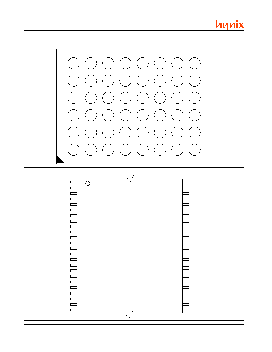
PIN CONFIGURATIONS
A 6
B 6
C 6
D 6
E 6
F 6
G 6
H 6
A 5
B 5
C 5
D 5
E 5
F 5
G 5
H 5
A 4
B 4
C 4
D 4
E 4
F 4
G 4
H 4
A 3
B 3
C 3
D 3
E 3
F 3
G 3
H 3
A 2
B 2
C 2
D 2
E 2
F 2
G 2
H 2
A 1
B 1
C 1
D 1
E 1
F 1
G 1
H 1
A [ 1 3 ]
A [ 1 2 ]
A [ 1 4 ]
A [ 1 5 ]
A [ 1 6 ]
B Y T E #
D Q [ 1 5 ] / A [ - 1 ]
V
S S
A[9]
A[8]
A[10]
A[11]
D Q [ 7 ]
D Q [ 1 4 ]
D Q [ 1 3 ]
D Q [ 6 ]
W E #
R E S E T #
N C
A [ 1 9 ]
D Q [ 5 ]
D Q [ 1 2 ]
V
C C
D Q [ 4 ]
R Y / B Y #
N C
A [ 1 8 ]
N C
D Q [ 2 ]
D Q [ 1 0 ]
D Q [ 1 1 ]
D Q [ 3 ]
A[7]
A[17]
A[6]
A[5]
D Q [ 0 ]
D Q [ 8 ]
D Q [ 9 ]
D Q [ 1 ]
A[3]
A[4]
A[2]
A[1]
A[0]
C E #
O E #
V
S S
48-Ball FBGA (Top View, Balls Facing Down)
TSOP48
A[11]
A[10]
5
6
A[9]
A[8]
7
8
A[19]
N C
9
10
W E #
RESET#
11
12
N C
N C
13
14
RY/BY#
A[18]
15
16
A[17]
A[7]
17
18
A[6]
A[5]
19
20
A[15]
A[14]
1
2
A[13]
A[12]
3
4
A[4]
A[3]
21
22
A[2]
A[1]
23
24
DQ[7]
DQ[14]
44
43
DQ[6]
DQ[13]
42
41
DQ[5]
DQ[12]
40
39
DQ[4]
V
C C
38
37
DQ[11]
DQ[3]
36
35
DQ[10]
DQ[2]
34
33
DQ[9]
DQ[1]
32
31
DQ[8]
DQ[0]
30
29
A[16]
BYTE#
48
47
V
S S
DQ[15]/A[-1]
46
45
O E #
V
S S
28
27
CE#
A[0]
26
25

5
Rev. 1.2/May 01
HY29LV160
CONVENTIONS
Unless otherwise noted, a positive logic (active
High) convention is assumed throughout this docu-
ment, whereby the presence at a pin of a higher,
more positive voltage (V
IH
) causes assertion of the
signal. A `#' symbol following the signal name, e.g.,
RESET#, indicates that the signal is asserted in
the Low state (V
IL
). See DC specifications for V
IH
and V
IL
values.
Whenever a signal is separated into numbered
bits, e.g., DQ[7], DQ[6], ..., DQ[0], the family of
bits may also be shown collectively, e.g., as
DQ[7:0].
The designation 0xNNNN (N = 0, 1, 2, . . . , 9, A, .
. . , E, F) indicates a number expressed in hexadeci-
mal notation. The designation 0bXXXX indicates a
number expressed in binary notation (X = 0, 1).
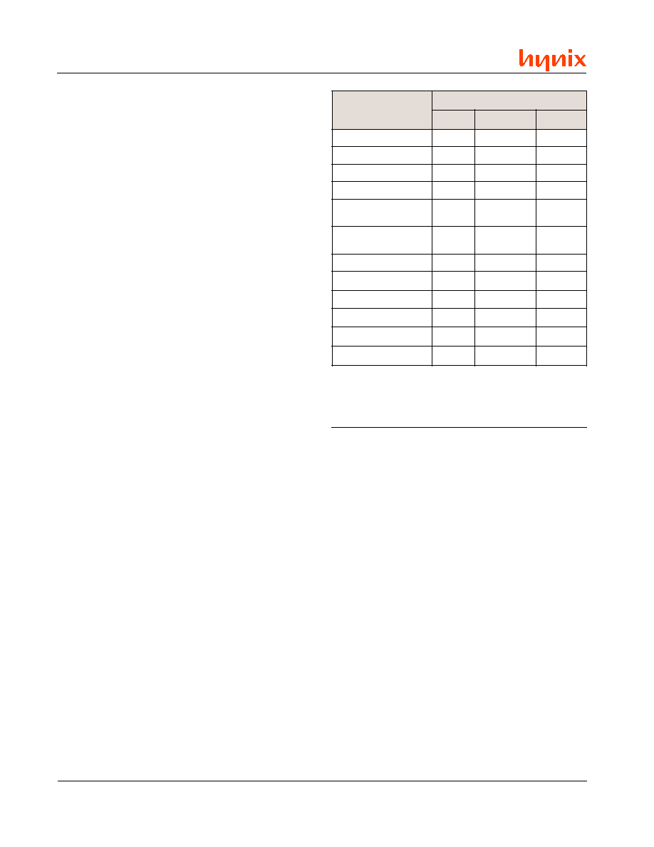
MEMORY ARRAY ORGANIZATION
The 16 Mbit Flash memory array is organized into
35 blocks called sectors (S0, S1, . . . , S34). A
sector is the smallest unit that can be erased and
that can be protected to prevent accidental or un-
authorized erasure. See the `Bus Operations' and
`Command Definitions' sections of this document
for additional information on these functions.
In the HY29LV160, four of the sectors, which com-
prise the boot block, vary in size from 8 to 32
Kbytes (4 to 16 Kwords), while the remaining 31
sectors are uniformly sized at 64 Kbytes (32
Kwords). The boot block can be located at the
bottom of the address range (HY29LV160B) or at
the top of the address range (HY29LV160T).
Tables 1 and 2 define the sector addresses and
corresponding address ranges for the top and bot-
tom boot block versions of the HY29LV160.
BUS OPERATIONS
Device bus operations are initiated through the
internal command register, which consists of sets
of latches that store the commands, along with
the address and data information, if any, needed
to execute the specific command. The command
register itself does not occupy any addressable
memory location. The contents of the command
register serve as inputs to an internal state ma-
chine whose outputs control the operation of the
device. Table 3 lists the normal bus operations,
the inputs and control levels they require, and the
resulting outputs. Certain bus operations require
a high voltage on one or more device pins. Those
are described in Table 4.
Read Operation
Data is read from the HY29LV160 by using stan-
dard microprocessor read cycles while placing the
byte or word address on the device's address in-
puts. The host system must drive the CE# and
OE# pins LOW and drive WE# high for a valid
read operation to take place. The BYTE# pin de-
termines whether the device outputs array data in
words (DQ[15:0]) or in bytes (DQ[7:0]).
The HY29LV160 is automatically set for reading
array data after device power-up and after a hard-
ware reset to ensure that no spurious alteration of
the memory content occurs during the power tran-
sition. No command is necessary in this mode to
obtain array data, and the device remains enabled
for read accesses until the command register con-
tents are altered.
This device features an Erase Suspend mode.
While in this mode, the host may read the array
data from any sector of memory that is not marked
for erasure. If the host reads from an address
within an erase-suspended (or erasing) sector, or
while the device is performing a byte or word pro-
gram operation, the device outputs status data
instead of array data. After completing an Auto-
matic Program or Automatic Erase algorithm within
a sector, that sector automatically returns to the
read array data mode. After completing a program-
ming operation in the Erase Suspend mode, the
system may once again read array data with the
same exception noted above.
The host must issue a hardware reset or the soft-
ware reset command to return a sector to the read
array data mode if DQ[5] goes high during a pro-
gram or erase cycle, or to return the device to the
read array data mode while it is in the Electronic
ID mode.
6
Rev. 1.2/May 01
HY29LV160
Table 1. HY29LV160T (Top Boot Block) Memory Array Organization
-
t
c
e
S
r
o
e
z
i
S
)
W
K
/
B
K
(
s
s
e
r
d
d
A
r
o
t
c
e
S
1
e
d
o
M
e
t
y
B
e
g
n
a
R
s
s
e
r
d
d
A
2
e
d
o
M
d
r
o
W
e
g
n
a
R
s
s
e
r
d
d
A
3
]
9
1
[
A
]
8
1
[
A
]
7
1
[
A
]
6
1
[
A
]
5
1
[
A
]
4
1
[
A
]
3
1
[
A
]
2
1
[
A
0
S
2
3
/
4
6
0
0
0
0
0
X
X
X
F
F
F
F
0
0
x
0
-
0
0
0
0
0
0
x
0
F
F
F
7
0
x
0
-
0
0
0
0
0
x
0
1
S
2
3
/
4
6
0
0
0
0
1
X
X
X
F
F
F
F
1
0
x
0
-
0
0
0
0
1
0
x
0
F
F
F
F
0
x
0
-
0
0
0
8
0
x
0
2
S
2
3
/
4
6
0
0
0
1
0
X
X
X
F
F
F
F
2
0
x
0
-
0
0
0
0
2
0
x
0
F
F
F
7
1
x
0
-
0
0
0
0
1
x
0
3
S
2
3
/
4
6
0
0
0
1
1
X
X
X
F
F
F
F
3
0
x
0
-
0
0
0
0
3
0
x
0
F
F
F
F
1
x
0
-
0
0
0
8
1
x
0
4
S
2
3
/
4
6
0
0
1
0
0
X
X
X
F
F
F
F
4
0
x
0
-
0
0
0
0
4
0
x
0
F
F
F
7
2
x
0
-
0
0
0
0
2
x
0
5
S
2
3
/
4
6
0
0
1
0
1
X
X
X
F
F
F
F
5
0
x
0
-
0
0
0
0
5
0
x
0
F
F
F
F
2
x
0
-
0
0
0
8
2
x
0
6
S
2
3
/
4
6
0
0
1
1
0
X
X
X
F
F
F
F
6
0
x
0
-
0
0
0
0
6
0
x
0
F
F
F
7
3
x
0
-
0
0
0
0
3
x
0
7
S
2
3
/
4
6
0
0
1
1
1
X
X
X
F
F
F
F
7
0
x
0
-
0
0
0
0
7
0
x
0
F
F
F
F
3
x
0
-
0
0
0
8
3
x
0
8
S
2
3
/
4
6
0
1
0
0
0
X
X
X
F
F
F
F
8
0
x
0
-
0
0
0
0
8
0
x
0
F
F
F
7
4
x
0
-
0
0
0
0
4
x
0
9
S
2
3
/
4
6
0
1
0
0
1
X
X
X
F
F
F
F
9
0
x
0
-
0
0
0
0
9
0
x
0
F
F
F
F
4
x
0
-
0
0
0
8
4
x
0
0
1
S
2
3
/
4
6
0
1
0
1
0
X
X
X
F
F
F
F
A
0
x
0
-
0
0
0
0
A
0
x
0
F
F
F
7
5
x
0
-
0
0
0
0
5
x
0
1
1
S
2
3
/
4
6
0
1
0
1
1
X
X
X
F
F
F
F
B
0
x
0
-
0
0
0
0
B
0
x
0
F
F
F
F
5
x
0
-
0
0
0
8
5
x
0
2
1
S
2
3
/
4
6
0
1
1
0
0
X
X
X
F
F
F
F
C
0
x
0
-
0
0
0
0
C
0
x
0
F
F
F
7
6
x
0
-
0
0
0
0
6
x
0
3
1
S
2
3
/
4
6
0
1
1
0
1
X
X
X
F
F
F
F
D
0
x
0
-
0
0
0
0
D
0
x
0
F
F
F
F
6
x
0
-
0
0
0
8
6
x
0
4
1
S
2
3
/
4
6
0
1
1
1
0
X
X
X
F
F
F
F
E
0
x
0
-
0
0
0
0
E
0
x
0
F
F
F
7
7
x
0
-
0
0
0
0
7
x
0
5
1
S
2
3
/
4
6
0
1
1
1
1
X
X
X
F
F
F
F
F
0
x
0
-
0
0
0
0
F
0
x
0
F
F
F
F
7
x
0
-
0
0
0
8
7
x
0
6
1
S
2
3
/
4
6
1
0
0
0
0
X
X
X
F
F
F
F
0
1
x
0
-
0
0
0
0
0
1
x
0
F
F
F
7
8
x
0
-
0
0
0
0
8
x
0
7
1
S
2
3
/
4
6
1
0
0
0
1
X
X
X
F
F
F
F
1
1
x
0
-
0
0
0
0
1
1
x
0
F
F
F
F
8
x
0
-
0
0
0
8
8
x
0
8
1
S
2
3
/
4
6
1
0
0
1
0
X
X
X
F
F
F
F
2
1
x
0
-
0
0
0
0
2
1
x
0
F
F
F
7
9
x
0
-
0
0
0
0
9
x
0
9
1
S
2
3
/
4
6
1
0
0
1
1
X
X
X
F
F
F
F
3
1
x
0
-
0
0
0
0
3
1
x
0
F
F
F
F
9
x
0
-
0
0
0
8
9
x
0
0
2
S
2
3
/
4
6
1
0
1
0
0
X
X
X
F
F
F
F
4
1
x
0
-
0
0
0
0
4
1
x
0
F
F
F
7
A
x
0
-
0
0
0
0
A
x
0
1
2
S
2
3
/
4
6
1
0
1
0
1
X
X
X
F
F
F
F
5
1
x
0
-
0
0
0
0
5
1
x
0
F
F
F
F
A
x
0
-
0
0
0
8
A
x
0
2
2
S
2
3
/
4
6
1
0
1
1
0
X
X
X
F
F
F
F
6
1
x
0
-
0
0
0
0
6
1
x
0
F
F
F
7
B
x
0
-
0
0
0
0
B
x
0
3
2
S
2
3
/
4
6
1
0
1
1
1
X
X
X
F
F
F
F
7
1
x
0
-
0
0
0
0
7
1
x
0
F
F
F
F
B
x
0
-
0
0
0
8
B
x
0
4
2
S
2
3
/
4
6
1
1
0
0
0
X
X
X
F
F
F
F
8
1
x
0
-
0
0
0
0
8
1
x
0
F
F
F
7
C
x
0
-
0
0
0
0
C
x
0
5
2
S
2
3
/
4
6
1
1
0
0
1
X
X
X
F
F
F
F
9
1
x
0
-
0
0
0
0
9
1
x
0
F
F
F
F
C
x
0
-
0
0
0
8
C
x
0
6
2
S
2
3
/
4
6
1
1
0
1
0
X
X
X
F
F
F
F
A
1
x
0
-
0
0
0
0
A
1
x
0
F
F
F
7
D
x
0
-
0
0
0
0
D
x
0
7
2
S
2
3
/
4
6
1
1
0
1
1
X
X
X
F
F
F
F
B
1
x
0
-
0
0
0
0
B
1
x
0
F
F
F
F
D
x
0
-
0
0
0
8
D
x
0
8
2
S
2
3
/
4
6
1
1
1
0
0
X
X
X
F
F
F
F
C
1
x
0
-
0
0
0
0
C
1
x
0
F
F
F
7
E
x
0
-
0
0
0
0
E
x
0
9
2
S
2
3
/
4
6
1
1
1
0
1
X
X
X
F
F
F
F
D
1
x
0
-
0
0
0
0
D
1
x
0
F
F
F
F
E
x
0
-
0
0
0
8
E
x
0
0
3
S
2
3
/
4
6
1
1
1
1
0
X
X
X
F
F
F
F
E
1
x
0
-
0
0
0
0
E
1
x
0
F
F
F
7
F
x
0
-
0
0
0
0
F
x
0
1
3
S
6
1
/
2
3
1
1
1
1
1
0
X
X
F
F
F
7
F
1
x
0
-
0
0
0
0
F
1
x
0
F
F
F
B
F
x
0
-
0
0
0
8
F
x
0
2
3
S
4
/
8
1
1
1
1
1
1
0
0
F
F
F
9
F
1
x
0
-
0
0
0
8
F
1
x
0
F
F
F
C
F
x
0
-
0
0
0
C
F
x
0
3
3
S
4
/
8
1
1
1
1
1
1
0
1
F
F
F
B
F
1
x
0
-
0
0
0
A
F
1
x
0
F
F
F
D
F
x
0
-
0
0
0
D
F
X
0
4
3
S
8
/
6
1
1
1
1
1
1
1
1
X
F
F
F
F
F
1
x
0
-
0
0
0
C
F
1
x
0
F
F
F
F
F
x
0
-
0
0
0
E
F
x
0
Notes:
1. `X' indicates don't care.
2. `0xN. . . N' indicates an address in hexadecimal notation.
3. The address range in byte mode is A[19:0, -1]. The address range in word mode is A[19:0].
7
Rev. 1.2/May 01
HY29LV160
Table 2. HY29LV160B (Bottom Boot Block) Memory Array Organization
Notes:
1. `X' indicates don't care.
2. `0xN. . . N' indicates an address in hexadecimal notation.
3. The address range in byte mode is A[19:0, -1]. The address range in word mode is A[19:0].
-
t
c
e
S
r
o
e
z
i
S
)
W
K
/
B
K
(
s
s
e
r
d
d
A
r
o
t
c
e
S
1
e
d
o
M
e
t
y
B
e
g
n
a
R
s
s
e
r
d
d
A
2
e
d
o
M
d
r
o
W
e
g
n
a
R
s
s
e
r
d
d
A
3
]
9
1
[
A
]
8
1
[
A
]
7
1
[
A
]
6
1
[
A
]
5
1
[
A
]
4
1
[
A
]
3
1
[
A
]
2
1
[
A
0
S
8
/
6
1
0
0
0
0
0
0
0
X
F
F
F
3
0
0
x
0
-
0
0
0
0
0
0
x
0
F
F
F
1
0
x
0
-
0
0
0
0
0
x
0
1
S
4
/
8
0
0
0
0
0
0
1
0
F
F
F
5
0
0
x
0
-
0
0
0
4
0
0
x
0
F
F
F
2
0
x
0
-
0
0
0
2
0
x
0
2
S
4
/
8
0
0
0
0
0
0
1
1
F
F
F
7
0
0
x
0
-
0
0
0
6
0
0
x
0
F
F
F
3
0
x
0
-
0
0
0
3
0
X
0
3
S
6
1
/
2
3
0
0
0
0
0
1
X
X
F
F
F
F
0
0
x
0
-
0
0
0
8
0
0
x
0
F
F
F
7
0
x
0
-
0
0
0
4
0
x
0
4
S
2
3
/
4
6
0
0
0
0
1
X
X
X
F
F
F
F
1
0
x
0
-
0
0
0
0
1
0
x
0
F
F
F
F
0
x
0
-
0
0
0
8
0
x
0
5
S
2
3
/
4
6
0
0
0
1
0
X
X
X
F
F
F
F
2
0
x
0
-
0
0
0
0
2
0
x
0
F
F
F
7
1
x
0
-
0
0
0
0
1
x
0
6
S
2
3
/
4
6
0
0
0
1
1
X
X
X
F
F
F
F
3
0
x
0
-
0
0
0
0
3
0
x
0
F
F
F
F
1
x
0
-
0
0
0
8
1
x
0
7
S
2
3
/
4
6
0
0
1
0
0
X
X
X
F
F
F
F
4
0
x
0
-
0
0
0
0
4
0
x
0
F
F
F
7
2
x
0
-
0
0
0
0
2
x
0
8
S
2
3
/
4
6
0
0
1
0
1
X
X
X
F
F
F
F
5
0
x
0
-
0
0
0
0
5
0
x
0
F
F
F
F
2
x
0
-
0
0
0
8
2
x
0
9
S
2
3
/
4
6
0
0
1
1
0
X
X
X
F
F
F
F
6
0
x
0
-
0
0
0
0
6
0
x
0
F
F
F
7
3
x
0
-
0
0
0
0
3
x
0
0
1
S
2
3
/
4
6
0
0
1
1
1
X
X
X
F
F
F
F
7
0
x
0
-
0
0
0
0
7
0
x
0
F
F
F
F
3
x
0
-
0
0
0
8
3
x
0
1
1
S
2
3
/
4
6
0
1
0
0
0
X
X
X
F
F
F
F
8
0
x
0
-
0
0
0
0
8
0
x
0
F
F
F
7
4
x
0
-
0
0
0
0
4
x
0
2
1
S
2
3
/
4
6
0
1
0
0
1
X
X
X
F
F
F
F
9
0
x
0
-
0
0
0
0
9
0
x
0
F
F
F
F
4
x
0
-
0
0
0
8
4
x
0
3
1
S
2
3
/
4
6
0
1
0
1
0
X
X
X
F
F
F
F
A
0
x
0
-
0
0
0
0
A
0
x
0
F
F
F
7
5
x
0
-
0
0
0
0
5
x
0
4
1
S
2
3
/
4
6
0
1
0
1
1
X
X
X
F
F
F
F
B
0
x
0
-
0
0
0
0
B
0
x
0
F
F
F
F
5
x
0
-
0
0
0
8
5
x
0
5
1
S
2
3
/
4
6
0
1
1
0
0
X
X
X
F
F
F
F
C
0
x
0
-
0
0
0
0
C
0
x
0
F
F
F
7
6
x
0
-
0
0
0
0
6
x
0
6
1
S
2
3
/
4
6
0
1
1
0
1
X
X
X
F
F
F
F
D
0
x
0
-
0
0
0
0
D
0
x
0
F
F
F
F
6
x
0
-
0
0
0
8
6
x
0
7
1
S
2
3
/
4
6
0
1
1
1
0
X
X
X
F
F
F
F
E
0
x
0
-
0
0
0
0
E
0
x
0
F
F
F
7
7
x
0
-
0
0
0
0
7
x
0
8
1
S
2
3
/
4
6
0
1
1
1
1
X
X
X
F
F
F
F
F
0
x
0
-
0
0
0
0
F
0
x
0
F
F
F
F
7
x
0
-
0
0
0
8
7
x
0
9
1
S
2
3
/
4
6
1
0
0
0
0
X
X
X
F
F
F
F
0
1
x
0
-
0
0
0
0
0
1
x
0
F
F
F
7
8
x
0
-
0
0
0
0
8
x
0
0
2
S
2
3
/
4
6
1
0
0
0
1
X
X
X
F
F
F
F
1
1
x
0
-
0
0
0
0
1
1
x
0
F
F
F
F
8
x
0
-
0
0
0
8
8
x
0
1
2
S
2
3
/
4
6
1
0
0
1
0
X
X
X
F
F
F
F
2
1
x
0
-
0
0
0
0
2
1
x
0
F
F
F
7
9
x
0
-
0
0
0
0
9
x
0
2
2
S
2
3
/
4
6
1
0
0
1
1
X
X
X
F
F
F
F
3
1
x
0
-
0
0
0
0
3
1
x
0
F
F
F
F
9
x
0
-
0
0
0
8
9
x
0
3
2
S
2
3
/
4
6
1
0
1
0
0
X
X
X
F
F
F
F
4
1
x
0
-
0
0
0
0
4
1
x
0
F
F
F
7
A
x
0
-
0
0
0
0
A
x
0
4
2
S
2
3
/
4
6
1
0
1
0
1
X
X
X
F
F
F
F
5
1
x
0
-
0
0
0
0
5
1
x
0
F
F
F
F
A
x
0
-
0
0
0
8
A
x
0
5
2
S
2
3
/
4
6
1
0
1
1
0
X
X
X
F
F
F
F
6
1
x
0
-
0
0
0
0
6
1
x
0
F
F
F
7
B
x
0
-
0
0
0
0
B
x
0
6
2
S
2
3
/
4
6
1
0
1
1
1
X
X
X
F
F
F
F
7
1
x
0
-
0
0
0
0
7
1
x
0
F
F
F
F
B
x
0
-
0
0
0
8
B
x
0
7
2
S
2
3
/
4
6
1
1
0
0
0
X
X
X
F
F
F
F
8
1
x
0
-
0
0
0
0
8
1
x
0
F
F
F
7
C
x
0
-
0
0
0
0
C
x
0
8
2
S
2
3
/
4
6
1
1
0
0
1
X
X
X
F
F
F
F
9
1
x
0
-
0
0
0
0
9
1
x
0
F
F
F
F
C
x
0
-
0
0
0
8
C
x
0
9
2
S
2
3
/
4
6
1
1
0
1
0
X
X
X
F
F
F
F
A
1
x
0
-
0
0
0
0
A
1
x
0
F
F
F
7
D
x
0
-
0
0
0
0
D
x
0
0
3
S
2
3
/
4
6
1
1
0
1
1
X
X
X
F
F
F
F
B
1
x
0
-
0
0
0
0
B
1
x
0
F
F
F
F
D
x
0
-
0
0
0
8
D
x
0
1
3
S
2
3
/
4
6
1
1
1
0
0
X
X
X
F
F
F
F
C
1
x
0
-
0
0
0
0
C
1
x
0
F
F
F
7
E
x
0
-
0
0
0
0
E
x
0
2
3
S
2
3
/
4
6
1
1
1
0
1
X
X
X
F
F
F
F
D
1
x
0
-
0
0
0
0
D
1
x
0
F
F
F
F
E
x
0
-
0
0
0
8
E
x
0
3
3
S
2
3
/
4
6
1
1
1
1
0
X
X
X
F
F
F
F
E
1
x
0
-
0
0
0
0
E
1
x
0
F
F
F
7
F
x
0
-
0
0
0
0
F
x
0
4
3
S
2
3
/
4
6
1
1
1
1
1
X
X
X
F
F
F
F
F
1
x
0
-
0
0
0
0
F
1
x
0
F
F
F
F
F
x
0
-
0
0
0
8
F
x
0
8
Rev. 1.2/May 01
HY29LV160
Table 3. HY29LV160 Normal Bus Operations
1
Notes:
1. L = V
IL
, H = V
IH
, X = Don't Care (L or H), D
OUT
= Data Out, D
IN
= Data In. See DC Characteristics for voltage levels.
2. Address is A[19:0, -1] in Byte Mode and A[19:0] in Word Mode.
3. DQ[15] is the A[-1] input in Byte Mode (BYTE# = L).
n
o
i
t
a
r
e
p
O
#
E
C
#
E
O
#
E
W
#
T
E
S
E
R
s
s
e
r
d
d
A
2
]
0
:
7
[
Q
D
]
8
:
5
1
[
Q
D
3
H
=
#
E
T
Y
B
L
=
#
E
T
Y
B
d
a
e
R
L
L
H
H
A
N
I
D
T
U
O
D
T
U
O
Z
-
h
g
i
H
e
t
i
r
W
L
H
L
H
A
N
I
D
N
I
D
N
I
Z
-
h
g
i
H
e
l
b
a
s
i
D
t
u
p
t
u
O
L
H
H
H
X
Z
-
h
g
i
H
Z
-
h
g
i
H
Z
-
h
g
i
H
y
b
d
n
a
t
S
l
a
m
r
o
N
#
E
C
H
X
X
H
X
Z
-
h
g
i
H
Z
-
h
g
i
H
Z
-
h
g
i
H
y
b
d
n
a
t
S
p
e
e
D
#
E
C
V
C
C
V
3
.
0
±
X
X
V
C
C
V
3
.
0
±
X
Z
-
h
g
i
H
Z
-
h
g
i
H
Z
-
h
g
i
H
t
e
s
e
R
e
r
a
w
d
r
a
H
)
y
b
d
n
a
t
S
l
a
m
r
o
N
(
X
X
X
L
X
Z
-
h
g
i
H
Z
-
h
g
i
H
Z
-
h
g
i
H
t
e
s
e
R
e
r
a
w
d
r
a
H
)
y
b
d
n
a
t
S
p
e
e
D
(
X
X
X
V
S
S
V
3
.
0
±
X
Z
-
h
g
i
H
Z
-
h
g
i
H
Z
-
h
g
i
H
Table 4. HY29LV160 Bus Operations Requiring High Voltage
1, 2
Notes:
1. L = V
IL
, H = V
IH
, X = Don't Care (L OR H). See DC Characteristics for voltage levels.
2. Address bits not specified are Don't Care.
3. See text and Appendix A for additional information.
4. SA = Sector Address. See Tables 1 and 2.
5. DQ[15] is the A[-1] input in Byte Mode (BYTE# = L).
6. Normal read, write and output disable operations are used in this mode. See Table 3.
n
o
i
t
a
r
e
p
O
3
#
E
C
#
E
O
#
E
W
#
T
E
S
E
R
]
2
1
:
9
1
[
A
]
9
[
A
]
6
[
A
]
1
[
A
]
0
[
A
]
0
:
7
[
Q
D
]
8
:
5
1
[
Q
D
#
E
T
Y
B
H
=
#
E
T
Y
B
L
=
5
t
c
e
t
o
r
P
r
o
t
c
e
S
L
H
L
V
D
I
A
S
4
X
L
H
L
D
N
I
X
X
t
c
e
t
o
r
p
n
U
r
o
t
c
e
S
L
H
L
V
D
I
X
X
H
H
L
D
N
I
X
X
r
o
t
c
e
S
y
r
a
r
o
p
m
e
T
t
c
e
t
o
r
p
n
U
6
-
-
-
-
-
-
V
D
I
-
-
-
-
-
-
-
-
-
-
-
-
-
-
-
-
e
d
o
C
r
e
r
u
t
c
a
f
u
n
a
M
L
L
H
H
X
V
D
I
L
L
L
D
A
x
0
X
Z
-
h
g
i
H
e
c
i
v
e
D
e
d
o
C
B
0
6
1
V
L
9
2
Y
H
L
L
H
H
X
V
D
I
L
L
H
9
4
x
0
2
2
x
0
Z
-
h
g
i
H
T
0
6
1
V
L
9
2
Y
H
4
C
x
0
n
o
i
t
c
e
t
o
r
P
r
o
t
c
e
S
n
o
i
t
a
c
i
f
i
r
e
V
L
L
H
H
A
S
4
V
D
I
L
H
L
=
0
0
x
0
d
e
t
c
e
t
o
r
p
n
U
X
Z
-
h
g
i
H
=
1
0
x
0
d
e
t
c
e
t
o
r
P

9
Rev. 1.2/May 01
HY29LV160
Write Operation
Certain operations, including programming data
and erasing sectors of memory, require the host
to write a command or command sequence to the
HY29LV160. Writes to the device are performed
by placing the byte or word address on the device's
address inputs while the data to be written is input
on DQ[15:0] (BYTE# = High) or DQ[7:0] (BYTE#
= Low). The host system must drive the CE# and
WE# pins Low and drive OE# High for a valid write
operation to take place. All addresses are latched
on the falling edge of WE# or CE#, whichever
happens later. All data is latched on the rising edge
of WE# or CE#, whichever happens first.
The "Device Commands" section of this data sheet
provides details on the specific device commands
implemented in the HY29LV160.
Standby Operation
When the system is not reading or writing to the
device, it can place the HY29LV160 in the Standby
mode. In this mode, current consumption is greatly
reduced, and the data bus outputs are placed in
the high impedance state, independent of the OE#
input. The Standby mode can be invoked using
two methods.
The device enters the CE# Deep Standby mode
when the CE# and RESET# pins are both held at
V
CC
± 0.3V. Note that this is a more restricted
voltage range than V
IH
. If both CE# and RESET#
are held at V
IH
, but not within V
CC
± 0.3V, the de-
vice will be in the CE# Normal Standby mode, but
the standby current will be greater.
The device enters the RESET# Deep Standby
mode when the RESET# pin is held at V
SS
± 0.3V.
If RESET# is held at V
IL
but not within V
SS
± 0.3V,
the device will be in the RESET# Normal Standby
mode, but the standby current will be greater. See
Reset Operation for additional information.
The device requires standard access time (t
CE
) for
read access when the device is in either of the
standby modes, before it is ready to read data. If
the device is deselected during erasure or pro-
gramming, it continues to draw active current until
the operation is completed.
Sleep Mode
The sleep mode automatically minimizes device
power consumption. This mode is automatically
entered when addresses remain stable for t
ACC
+
30 ns (typical) and is independent of the state of
the CE#, WE#, and OE# control signals. Stan-
dard address access timings provide new data
when addresses are changed. While in sleep
mode, output data is latched and always available
to the system.
NOTE: Sleep mode is entered only when the device is
in read mode. It is not entered if the device is executing
an automatic algorithm, if it is in erase suspend mode,
or during receipt of a command sequence.
Output Disable Operation
When the OE# input is at V
IH
, output data from the
device is disabled and the data bus pins are placed
in the high impedance state.
Reset Operation
The RESET# pin provides a hardware method of
resetting the device to reading array data. When
the RESET# pin is driven low for the minimum
specified period, the device immediately termi-
nates any operation in progress, tri-states the data
bus pins, and ignores all read/write commands for
the duration of the RESET# pulse. The device also
resets the internal state machine to reading array
data. If an operation was interrupted by the as-
sertion of RESET#, it should be reinitiated once
the device is ready to accept another command
sequence to ensure data integrity.
Current is reduced for the duration of the RESET#
pulse as described in the Standby Operation sec-
tion above.
If RESET# is asserted during a program or erase
operation, the RY/BY# pin remains Low (busy) until
the internal reset operation is complete, which re-
quires a time of t
READY
(during Automatic Algo-
rithms). The system can thus monitor RY/BY# to
determine when the reset operation completes,
and can perform a read or write operation t
RB
after
RY/BY# goes High. If RESET# is asserted when
a program or erase operation is not executing (RY/
BY# pin is High), the reset operation is completed
within a time of t
RP
. In this case, the host can per-
form a read or write operation t
RH
after the RE-
SET# pin returns High .
The RESET# pin may be tied to the system reset
signal. Thus, a system reset would also reset the
device, enabling the system to read the boot-up
firmware from the Flash memory.
10
Rev. 1.2/May 01
HY29LV160
Sector Protect Operation
The hardware sector protection feature disables
both program and erase operations in any sector
or combination of sectors. This function can be
implemented either in-system or by using program-
ming equipment.
The method intended for programming equipment
requires a high voltage (V
ID
) on address pin A[9]
and the control pins. Refer to the Appendix at the
end of this document for additional information.
The in-system method requires V
ID
only on the
RESET# pin and uses standard microprocessor
bus cycle timing to implement sector protection.
The flow chart in Figure 1 illustrates the algorithm.
The HY29LV160 is shipped with all sectors un-
protected. It is possible to determine whether a
sector is protected or unprotected. See the Elec-
tronic ID Mode section for details.
Sector Unprotect Operation
The hardware sector unprotection feature re-en-
ables both program and erase operations in pre-
viously protected sectors. This function can be
implemented either in-system or by using program-
ming equipment. Note that to unprotect any sec-
S T A R T
R E S E T # = V
ID
Wait 1 us
Write 0x60 to device
Write 0x60 to Address
Wait 150 us
Write 0x40 to Address
R e a d f r o m A d d r e s s
Data = 0x01?
Protect Another
Sector?
Y E S
T R Y C N T = 2 5 ?
N O
I n c r e m e n t T R Y C N T
N O
Y E S
DEVICE FAILURE
Y E S
N O
R E S E T # = V
IH
W r i t e R e s e t C o m m a n d
SECTOR PROTECT
C O M P L E T E
T R Y C N T = 1
Set Address:
A[19:12] = Sector to Protect
A[6] = 0, A[1] = 1, A[0] = 0
Figure 1. Sector Protect Algorithm
tor, all unprotected sectors must first be protected
prior to the first sector unprotect write cycle. Also,
the unprotect procedure will cause all sectors to
become unprotected, thus, sectors that require
protection must be protected again after the un-
protect procedure is run.
The method intended for programming equipment
requires a high voltage (V
ID
) on address pin A[9]
and the control pins. Refer to the Appendix for
additional information.
The in-system method requires V
ID
only on the
RESET# pin and uses standard microprocessor
bus cycle timing to implement sector unprotection.
The flow chart in Figure 2 illustrates the algorithm.
Temporary Sector Unprotect Operation
This feature allows temporary unprotection of pre-
viously protected sectors to allow changing the
data in-system. Sector Unprotect mode is activated
by setting the RESET# pin to V
ID
. While in this
mode, formerly protected sectors can be pro-
grammed or erased by invoking the appropriate
commands (see Device Commands section).
Once V
ID
is removed from RESET#, all the previ-
ously protected sectors are protected again. Fig-
ure 3 illustrates the algorithm.
11
Rev. 1.2/May 01
HY29LV160
S T A R T
(Note: All sectors must be
protected prior to
unprotecting any sector)
T R Y C N T = 1
S N U M = 0
R E S E T # = V
ID
Wait 1 us
Write 0x60 to device
Write 0x60 to Address
Set Address:
A[19:12] = Sector SNUM
A[6] = 1, A]1] = 1, A]0] = 0
Write 0x40 to Address
R e a d f r o m A d d r e s s
Data = 0x00?
S N U M = 3 4 ?
Y E S
T R Y C N T = 1 0 0 0 ?
N O
I n c r e m e n t T R Y C N T
N O
Y E S
DEVICE FAILURE
Y E S
N O
R E S E T # = V
IH
W r i t e R e s e t C o m m a n d
SECTOR UNPROTECT
C O M P L E T E
S N U M = S N U M + 1
W a i t 1 5 m s
Set Address:
A[6] = 1, A]1] = 1, A]0] = 0
Figure 2. Sector Unprotect Algorithm
S T A R T
R E S E T # = V
ID
(All protected sectors
b e c o m e u n p r o t e c t e d )
Perform Program or Erase
Operations
R E S E T # = V
IH
(All previously protected
sectors return to protected
state)
T E M P O R A R Y S E C T O R
U N P R O T E C T C O M P L E T E
Figure 3. Temporary Sector Unprotect
Algorithm
Electronic ID Operation (High Voltage Method)
The Electronic ID mode provides manufacturer and
device identification and sector protection verifi-
cation through codes output on DQ[15:0]. This
mode is intended primarily for programming equip-
ment to automatically match a device to be pro-
grammed with its corresponding programming al-
gorithm.
Two methods are provided for accessing the Elec-
tronic ID data. The first requires V
ID
on address
pin A[9], with additional requirements for obtain-
ing specific data items listed in Table 4. The Elec-
tronic ID data can also be obtained by the host
through specific commands issued via the com-
mand register, as described in the `Device Com-
mands' section of this data sheet.
While in the high-voltage Electronic ID mode, the
system may read at specific addresses to obtain
certain device identification and status informa-
tion:
A read cycle at address 0xXXX00 retrieves the
manufacturer code.
A read cycle at address 0xXXX01 in Word
mode or 0xXXX02 in Byte mode returns the
device code.
A read cycle containing a sector address (SA)
in A[19:12] and the address 0x02 in Word mode
or 0x04 in Byte mode, returns 0x01 if that sec-
tor is protected, or 0x00 if it is unprotected.
12
Rev. 1.2/May 01
HY29LV160
DEVICE COMMANDS
Device operations are initiated by writing desig-
nated address and data command sequences into
the device. Addresses are latched on the falling
edge of WE# or CE#, whichever happens later.
Data is latched on the rising edge of WE# or CE#,
whichever happens first.
A command sequence is composed of one, two
or three of the following sub-segments: an unlock
cycle, a command cycle and a data cycle. Table
5 summarizes the composition of the valid com-
mand sequences implemented in the HY29LV160,
and these sequences are fully described in Table
6 and in the sections that follow.
Writing incorrect address and data values or writ-
ing them in the improper sequence resets the
HY29LV160 to the Read mode.
Reading Data
The device automatically enters the Read mode
after device power-up, after the RESET# input is
asserted and upon the completion of certain com-
mands. Commands are not required to retrieve
data in this mode. See Read Operation section
for additional information.
Reset Command
Writing the Reset command resets the sectors to
the Read or Erase-Suspend mode. Address bits
are don't cares for this command.
As described above, a Reset command is not nor-
mally required to begin reading array data. How-
ever, a Reset command must be issued in order
to read array data in the following cases:
∑
If the device is in the Electronic ID mode, a
Reset command must be written to return to
the Read mode. If the device was in the Erase
Suspend mode when the device entered the
Electronic ID mode, writing the Reset command
returns the device to the Erase Suspend mode.
Note: When in the Electronic ID bus operation mode,
the device returns to the Read mode when V
ID
is re-
moved from the A[9] pin. The Reset command is not
required in this case.
∑
If the device is in the CFI Query mode, a Reset
command must be written to return to the ar-
ray Read mode.
d
n
a
m
m
o
C
e
c
n
e
u
q
e
S
s
e
l
c
y
C
s
u
B
f
o
r
e
b
m
u
N
k
c
o
l
n
U
d
n
a
m
m
o
C
a
t
a
D
t
e
s
e
R
0
1
0
d
a
e
R
0
0
1
e
t
o
N
m
a
r
g
o
r
P
d
r
o
W
/
e
t
y
B
2
1
1
s
s
a
p
y
B
k
c
o
l
n
U
2
1
0
s
s
a
p
y
B
k
c
o
l
n
U
t
e
s
e
R
0
1
1
s
s
a
p
y
B
k
c
o
l
n
U
m
a
r
g
o
r
P
d
r
o
W
/
e
t
y
B
0
1
1
e
s
a
r
E
p
i
h
C
4
1
1
e
s
a
r
E
r
o
t
c
e
S
4
1
)
2
e
t
o
N
(
1
d
n
e
p
s
u
S
e
s
a
r
E
0
1
0
e
m
u
s
e
R
e
s
a
r
E
0
1
0
D
I
c
i
n
o
r
t
c
e
l
E
2
1
3
e
t
o
N
y
r
e
u
Q
I
F
C
0
1
4
e
t
o
N
Notes:
1. Any number of Flash array read cycles are permitted.
2. Additional data cycles may follow. See text.
3. Any number of Electronic ID read cycles are permitted.
4. Any number of CFI data read cycles are permitted.
Table 5. Composition of Command Sequences
∑
If DQ[5] (Exceeded Time Limit) goes High dur-
ing a program or erase operation, a Reset com-
mand must be invoked to return the sectors to
the Read mode (or to the Erase Suspend mode
if the device was in Erase Suspend when the
Program command was issued).
The Reset command may also be used to abort
certain command sequences:
∑
In a Sector Erase or Chip Erase command se-
quence, the Reset command may be written
at any time before erasing actually begins, in-
cluding, for the Sector Erase command, be-
tween the cycles that specify the sectors to be
erased (see Sector Erase command descrip-
tion). This aborts the command and resets the
device to the Read mode. Once erasure be-
gins, however, the device ignores the Reset
command until the operation is complete.
∑
In a Program command sequence, the Reset
command may be written between the se-
quence cycles before programming actually be-
gins. This aborts the command and resets the
device to the Read mode, or to the Erase Sus-
pend mode if the Program command sequence
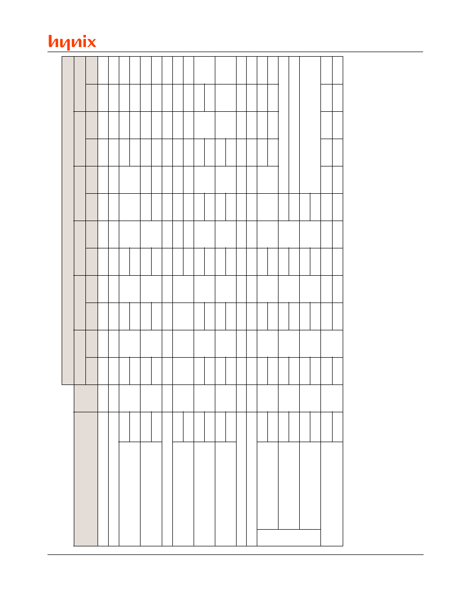
13
Rev. 1.2/May 01
HY29LV160
Table 6. HY29LV160 Command Sequences
Legend:
X = Don
'
t Care
PA = Address of the data to be programmed
RA = Memory address of data to be read
PD = Data to be programmed at address PA
RD
=
Data
read
from
location
RA
during
the
read
operation
SA = Sector address of sector to be erased or verified (see Note 3 and
Tables 1 and 2).
Notes:
See next page for notes.
Electronic ID
6
s
e
l
c
y
C
s
u
B
3
,
2
,
1
e
c
n
e
u
q
e
S
d
n
a
m
m
o
C
e
t
i
r
W
s
e
l
c
y
C
t
s
r
i
F
d
n
o
c
e
S
d
r
i
h
T
h
t
r
u
o
F
h
t
f
i
F
h
t
x
i
S
d
d
A
a
t
a
D
d
d
A
a
t
a
D
d
d
A
a
t
a
D
d
d
A
a
t
a
D
d
d
A
a
t
a
D
d
d
A
a
t
a
D
d
a
e
R0
A
RD
R
t
e
s
e
R
7
1X
X
X0
F
m
a
r
g
o
r
P
l
a
m
r
o
N
d
r
o
W
4
5
5
5
A
A
A
A
2
5
5
5
5
5
0
AA
PD
P
e
t
y
BA
A
A5
5
5A
A
A
s
s
a
p
y
B
k
c
o
l
n
U
d
r
o
W
3
5
5
5
A
A
A
A
2
5
5
5
5
5
0
2
e
t
y
BA
A
A5
5
5A
A
A
t
e
s
e
R
s
s
a
p
y
B
k
c
o
l
n
U2
X
X
X0
9X
X
X0
0
m
a
r
g
o
r
P
s
s
a
p
y
B
k
c
o
l
n
U
9
d
r
o
W
2X
X
X0
AA
PD
P
e
t
y
B
e
s
a
r
E
p
i
h
C
d
r
o
W
6
5
5
5
A
A
A
A
2
5
5
5
5
5
0
8
5
5
5
A
A
A
A
2
5
5
5
5
5
0
1
e
t
y
BA
A
A5
5
5A
A
AA
A
A5
5
5A
A
A
e
s
a
r
E
r
o
t
c
e
S
d
r
o
W
6
5
5
5
A
A
A
A
2
5
5
5
5
5
0
8
5
5
5
A
A
A
A
2
5
5A
S0
3
e
t
y
BA
A
A5
5
5A
A
AA
A
A5
5
5
d
n
e
p
s
u
S
e
s
a
r
E
4
1X
X
X0
B
e
m
u
s
e
R
e
s
a
r
E
5
1X
X
X0
3
e
d
o
C
r
e
r
u
t
c
a
f
u
n
a
M
d
r
o
W
3
5
5
5
A
A
A
A
2
5
5
5
5
5
0
90
0
XD
A
e
t
y
BA
A
A5
5
5A
A
A
e
d
o
C
e
c
i
v
e
D
d
r
o
W
3
5
5
5
A
A
A
A
2
5
5
5
5
5
0
9
1
0
X)
t
o
o
B
m
o
t
t
o
B
(
9
4
2
2
,
)
t
o
o
B
p
o
T
(
4
C
2
2
e
t
y
BA
A
A5
5
5A
A
A2
0
X)
t
o
o
B
m
o
t
t
o
B
(
9
4
,
)
t
o
o
B
p
o
T
(
4
C
y
f
i
r
e
V
t
c
e
t
o
r
P
r
o
t
c
e
S
d
r
o
W
3
5
5
5
A
A
A
A
2
5
5
5
5
5
0
9
2
0
X
)
A
S
(
r
o
t
c
e
S
d
e
t
c
e
t
o
r
p
n
U
=
0
0
r
o
t
c
e
S
d
e
t
c
e
t
o
r
P
=
1
0
e
t
y
BA
A
A5
5
5A
A
A4
0
X
)
A
S
(
)
I
F
C
(
e
c
a
f
r
e
t
n
I
h
s
a
l
F
n
o
m
m
o
C
y
r
e
u
Q
8
d
r
o
W
1
5
5
0
8
9
e
t
y
BA
A
0

14
Rev. 1.2/May 01
HY29LV160
Notes for Table 6:
1. All values are in hexadecimal. DQ[15:8] are don't care for unlock and command cycles.
2. All bus cycles are write operations unless otherwise noted.
3. Address is A[10:0] in Word mode and A[10:0, -1] in Byte mode. A[19:11] are don't care except as follows:
∑
For RA and PA, A[19:11] are the upper address bits of the byte to be read or programmed.
∑
For the sixth cycle of Sector Erase, SA = A[19:12] are the sector address of the sector to be erased.
∑
For the fourth cycle of Sector Protect Verify, SA = A[19:12] are the sector address of the sector to be verified.
4. The Erase Suspend command is valid only during a sector erase operation. The system may read and program in non-
erasing sectors, or enter the Electronic ID mode, while in the Erase Suspend mode.
5. The Erase Resume command is valid only during the Erase Suspend mode.
6. The fourth bus cycle is a read cycle.
7. The command is required only to return to the Read mode when the device is in the Electronic ID command mode or in
the CFI Query mode. It must also be issued to return to read mode if DQ[5] goes High during a program or erase
operation. It is not required for normal read operations.
8
This command is valid only when the device is in Read mode or in Electronic ID mode.
9. The Unlock Bypass command is required prior to the Unlock Bypass Program command.
is written while the device is in the Erase Sus-
pend mode. Once programming begins, how-
ever, the device ignores the Reset command
until the operation is complete.
∑
The Reset command may be written between
the cycles in an Electronic ID command se-
quence to abort that command. As described
above, once in the Electronic ID mode, the
Reset command must be written to return to
the array Read mode.
Program Command
The system programs the device a word or byte
at a time by issuing the appropriate four-cycle pro-
gram command sequence as shown in Table 6.
The sequence begins by writing two unlock cycles,
followed by the program setup command and,
lastly, the program address and data. This ini-
tiates the Automatic Program algorithm which au-
tomatically provides internally generated program
pulses and verifies the programmed cell margin.
The host is not required to provide further con-
trols or timings during this operation. When the
Automatic Program algorithm is complete, the de-
vice returns to the array Read mode (or to the
Erase Suspend mode if the device was in Erase
Suspend when the Program command was is-
sued). Several methods are provided to allow the
host to determine the status of the programming
operation, as described in the Write Operation
Status section.
Commands written to the device during execution
of the Automatic Program algorithm are ignored.
Note that a hardware reset immediately terminates
the programming operation. To ensure data in-
tegrity, the aborted Program command sequence
should be reinitiated once the reset operation is
complete.
Programming is allowed in any sequence. Only
erase operations can convert a stored "0" to a "1".
Thus, a bit cannot be programmed from a "0" back
to a "1". Attempting to do so may halt the opera-
tion and set DQ[5] to "1", or cause the Data# Poll-
ing algorithm to indicate the operation was suc-
cessful. However, a succeeding read will show
that the data is still "0".
Figure 4 illustrates the programming procedure.
Unlock Bypass/Bypass Program/Bypass Reset
Commands
Unlock bypass provides a faster method for the
host system to program the device. As shown in
Table 6, the Unlock Bypass command sequence
consists of two unlock write cycles followed by a
third write cycle containing the Unlock Bypass
command, 0x20. In the Unlock Bypass mode, a
two-cycle Unlock Bypass Program command se-
quence is used instead of the standard four-cycle
Program sequence to invoke a programming op-
eration. The first cycle in this sequence contains
the Unlock Bypass Program command, 0xA0, and
the second cycle specifies the program address
and data, thus eliminating the initial two unlock
cycles required in the standard Program command
sequence Additional data is programmed in the
same manner.
During the Unlock Bypass mode, only the Unlock
Bypass program and Unlock Bypass Reset com-
mands are valid. To exit the Unlock Bypass mode,
the host must issue the two-cycle Unlock Bypass
Reset command sequence shown in Table 6. The
device then returns to the array Read mode.
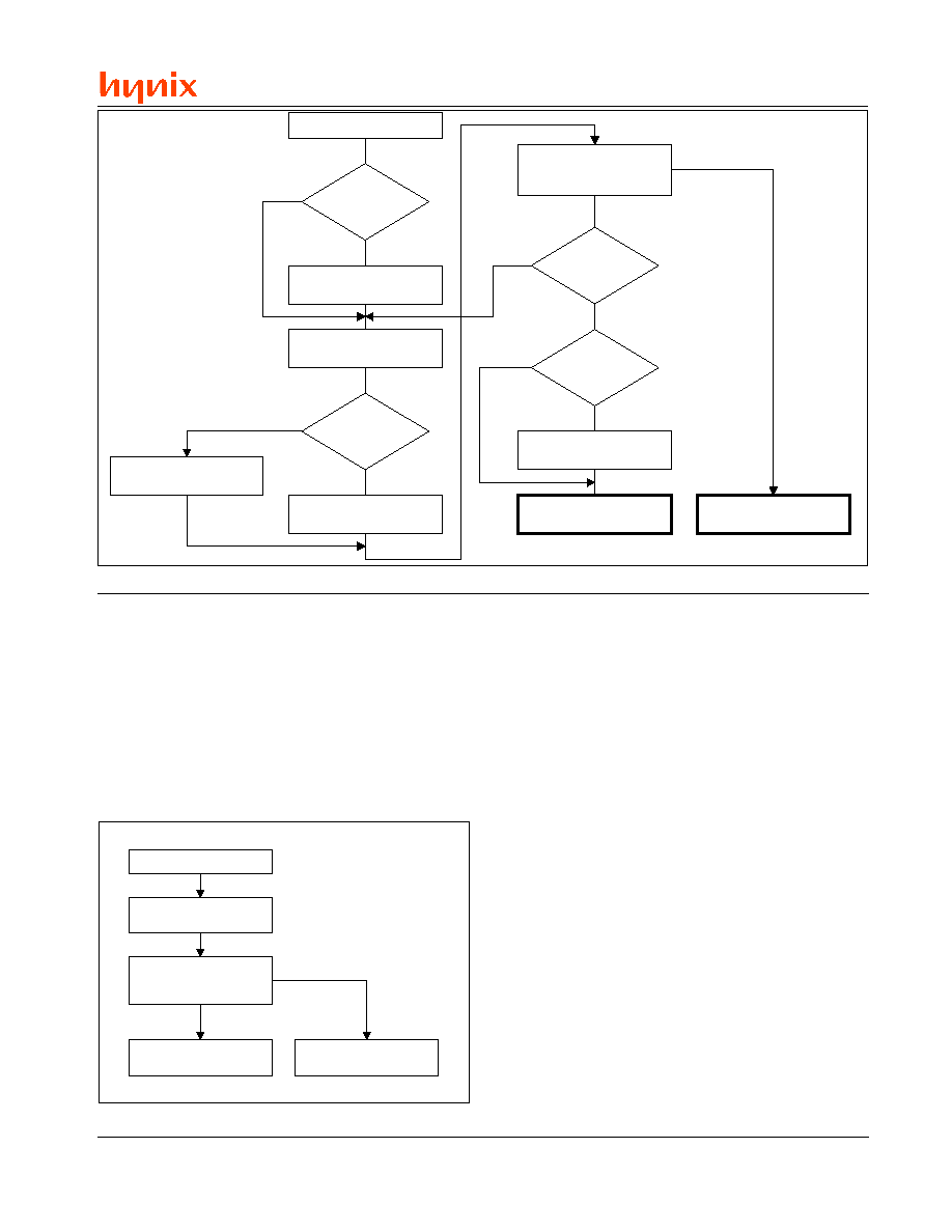
15
Rev. 1.2/May 01
HY29LV160
Chip Erase Command
The Chip Erase command sequence consists of
two unlock cycles, followed by a set-up command,
two additional unlock cycles and then the Chip
Erase command. This sequence invokes the Au-
tomatic Erase algorithm which automatically
preprograms and verifies the entire memory for
an all zero data pattern prior to electrical erase.
The host system is not required to provide any
controls or timings during these operations.
Figure 4. Normal and Unlock Bypass Programming Procedures
Figure 5. Chip Erase Procedure
START
I s s u e C H I P E R A S E
C o m m a n d S e q u e n c e
Check Erase Status
(See Write Operation Status
Section)
CHIP ERASE COMPLETE
GO TO
E R R O R R E C O V E R Y
DQ[5] Error Exit
Normal Exit
Commands written to the device during execution
of the Automatic Erase algorithm are ignored. Note
that a hardware reset immediately terminates the
chip erase operation. To ensure data integrity,
the aborted Chip Erase command sequence
should be reissued once the reset operation is
complete.
When the Automatic Erase algorithm is complete,
the device returns to the array Read mode. Sev-
eral methods are provided to allow the host to
determine the status of the erase operation, as
described in the Write Operation Status section.
Figure 5 illustrates the chip erase procedure.
Sector Erase Command
The Sector Erase command sequence consists
of two unlock cycles, followed by the Erase com-
mand, two additional unlock cycles and then the
sector erase data cycle, which specifies the sec-
tor to be erased. As described later in this sec-
tion, multiple sectors can be specified for erasure
with a single command sequence. During sector
erase, all specified sectors are erased sequen-
tially. The data in sectors not specified for era-
sure, as well as the data in any protected sectors,
S T A R T
Enable Fast
Programming?
I s s u e U N L O C K B Y P A S S
C o m m a n d
Y E S
N O
Unlock Bypass
M o d e ?
I s s u e U N L O C K B Y P A S S
P R O G R A M C o m m a n d
I s s u e N O R M A L P R O G R A M
C o m m a n d
Check Programming Status
(See Write Operation Status
Section)
Y E S
N O
Last Word/Byte
D o n e ?
Y E S
N O
Setup Next Address/Data for
Program Operation
Y E S
N O
Unlock Bypass
M o d e ?
I s s u e U N L O C K B Y P A S S
R E S E T C o m m a n d
P R O G R A M M I N G
C O M P L E T E
G O T O E R R O R
R E C O V E R Y P R O C E D U R E
DQ[5] Error Exit
Programming Verified
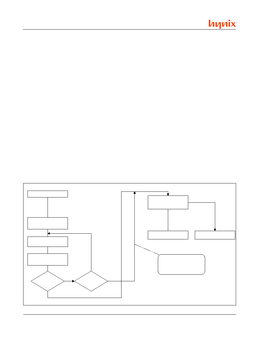
16
Rev. 1.2/May 01
HY29LV160
even if specified for erasure, is not affected by the
sector erase operation.
The Sector Erase command sequence starts the
Automatic Erase algorithm, which preprograms
and verifies the specified unprotected sectors for
an all zero data pattern prior to electrical erase.
The device then provides the required number of
internally generated erase pulses and verifies cell
erasure within the proper cell margins. The host
system is not required to provide any controls or
timings during these operations.
After the sector erase data cycle (the sixth bus
cycle) of the command sequence is issued, a sec-
tor erase time-out of 50 µs, measured from the
rising edge of the final WE# pulse in that bus cycle,
begins. During this time-out window, an additional
sector erase data cycle, specifying the sector ad-
dress of another sector to be erased, may be writ-
ten into an internal sector erase buffer. This buffer
may be loaded in any sequence, and the number
of sectors specified may be from one sector to all
sectors. The only restriction is that the time be-
tween these additional data cycles must be less
than 50 µs, otherwise erasure may begin before
the last data cycle is accepted. To ensure that all
data cycles are accepted, it is recommended that
host processor interrupts be disabled during the
START
YES
Erase An
Additional Sector?
Check Erase Status
(See Write Operation Status
Section)
Setup First (or Next) Sector
Address for Erase Operation
ERASE COMPLETE
Write First Five Cycles of
S E C T O R E R A S E
Command Sequence
Write Last Cycle (SA/0x30)
of SECTOR ERASE
Command Sequence
Sector Erase
Time-out (DQ[3])
Expired?
N O
YES
N O
GO TO
E R R O R R E C O V E R Y
DQ[5] Error Exit
Normal Exit
Sectors which require erasure
but which were not specified in
this erase cycle must be erased
later using a new command
sequence
Figure 6. Sector Erase Procedure
time that the additional cycles are being issued
and then be re-enabled afterwards.
If all sectors specified for erasing are protected,
the device returns to reading array data after ap-
proximately 100 µs. If at least one specified sec-
tor is not protected, the erase operation erases
the unprotected sectors, and ignores the command
for the sectors that are protected.
The system can monitor DQ[3] to determine if the
50 µs sector erase time-out has expired, as de-
scribed in the Write Operation Status section. If
the time between additional sector erase data
cycles can be insured to be less than the time-
out, the system need not monitor DQ[3].
Any command other than Sector Erase or Erase
Suspend during the time-out period resets the
device to reading array data. The system must
then rewrite the command sequence, including any
additional sector erase data cycles. Once the sec-
tor erase operation itself has begun, only the Erase
Suspend command is valid. All other commands
are ignored.
As for the Chip Erase command, note that a hard-
ware reset immediately terminates the sector
erase operation. To ensure data integrity, the

17
Rev. 1.2/May 01
HY29LV160
aborted Sector Erase command sequence should
be reissued once the reset operation is complete.
When the Automatic Erase algorithm terminates,
the device returns to the array Read mode. Sev-
eral methods are provided to allow the host to de-
termine the status of the erase operation, as de-
scribed in the Write Operation Status section.
Figure 6 illustrates the Sector Erase procedure.
Erase Suspend/Erase Resume Commands
The Erase Suspend command allows the system
to interrupt a sector erase operation to read data
from, or program data in, any sector not being
erased. The command causes the erase opera-
tion to be suspended in all sectors specified for
erasure. This command is valid only during the
sector erase operation, including during the 50 µs
time-out period at the end of the command se-
quence, and is ignored if it is issued during chip
erase or programming operations.
The HY29LV160 requires a maximum of 20 µs to
suspend the erase operation if the Erase Suspend
command is issued during sector erasure. How-
ever, if the command is written during the time-
out, the time-out is terminated and the erase op-
eration is suspended immediately. Once the erase
operation has been suspended, the system can
read array data from or program data to any sec-
tor not specified for erasure. Normal read and
write timings and command definitions apply.
Reading at any address within erase-suspended
sectors produces status data on DQ[7:0]. The host
can use DQ[7], or DQ[6] and DQ[2] together, to
determine if a sector is actively erasing or is erase-
suspended. See the Write Operation Status sec-
tion for information on these status bits.
After an erase-suspended program operation is
complete, the host can initiate another program-
ming operation (or read operation) within non-sus-
pended sectors. The host can determine the sta-
tus of a program operation during the Erase-Sus-
pended state just as in the standard programming
operation.
The host may also write the Electronic ID or CFI
Query command sequences when the device is
in the Erase Suspend mode. The device allows
reading Electronic ID and CFI codes even at ad-
dresses within erasing sectors, since the codes
are not stored in the memory array. When the
device exits the Electronic ID mode or the CFI
Query mode, the device reverts to the Erase Sus-
pend mode, and is ready for another valid opera-
tion. See Electronic ID and CFI Query Mode sec-
tions for more information.
The system must write the Erase Resume com-
mand to exit the Erase Suspend mode and con-
tinue the sector erase operation. Further writes of
the Resume command are ignored. Another Erase
Suspend command can be written after the de-
vice has resumed erasing.
Electronic ID Command
The Electronic ID mode provides manufacturer and
device identification and sector protection verifi-
cation through identifier codes output on DQ[7:0].
This mode is intended primarily for programming
equipment to automatically match a device to be
programmed with its corresponding programming
algorithm.
Two methods are provided for accessing the Elec-
tronic ID data. The first requires V
ID
on address
pin A[9], as described previously in the Device
Operations section.
The Electronic ID data can also be obtained by
the host by invoking the Electronic ID command,
as shown in Table 6. This method does not re-
quire V
ID
. The Electronic ID command sequence
may be issued while the device is in the Read
mode or in the Erase Suspend Read mode, that
is, except while programming or erasing.
The Electronic ID command sequence is initiated
by writing two unlock cycles, followed by the Elec-
tronic ID command. The device then enters the
Electronic ID mode, and the system may read at
any address any number of times, without initiat-
ing another command sequence.
∑
A read cycle at address 0xXXX00 retrieves the
manufacturer code.
∑
A read cycle at address 0xXXX01 in Word
mode or 0xXXX02 in Byte mode returns the
device code.
∑
A read cycle containing a sector address (SA)
in A[19:12] and the address 0x02 in A[7:0] in
Word mode (or 0x04 in A[6:0, -1] in Byte mode)
returns 0x01 if that sector is protected, or 0x00
if it is unprotected.
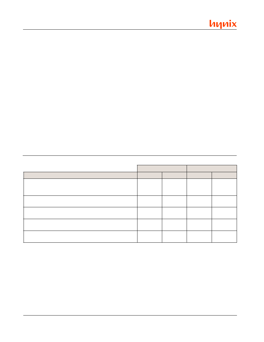
18
Rev. 1.2/May 01
HY29LV160
The system must write the Reset command to exit
the Electronic ID mode and return to reading ar-
ray data.
Query Command and Common Flash Inter-
face (CFI) Mode
The HY29LV160 is capable of operating in the
Common Flash Interface (CFI) mode. This mode
allows the host system to determine the manufac-
turer of the device, its operating parameters, its
configuration and any special command codes that
the device may accept. With this knowledge, the
system can optimize its use of the chip by using
appropriate timeout values, optimal voltages and
commands necessary to use the chip to its full
advantage.
Two commands are employed in association with
CFI mode. The first places the device in CFI mode
(Query command) and the second takes it out of
CFI mode (Reset command). These are described
in Table 6.
The single cycle Query command is valid only
when the device is in the Read mode, including
during Erase Suspend and Standby states and
while in Electronic ID mode, but is ignored other-
wise. Read cycles at appropriate addresses while
in the Query mode provide CFI data as described
later in this section. Write cycles are ignored, ex-
cept for the Reset command.
The Reset command returns the device from the
CFI mode to the array Read mode, or to the Erase
Suspend mode if the device was in that mode prior
to entering CFI mode, or to the Electronic ID mode
if the device was in that mode prior to entering
CFI mode. The command is valid only when the
device is in the CFI mode and as otherwise de-
scribed for the normal Reset command.
Tables 7 - 10 specify the data provided by the
HY29LV160 during CFI mode. Data at unspeci-
fied addresses reads out as 0x00. Note that a
value of 0x00 for a data item normally indicates
that the function is not supported. All values in
these tables are in hexadecimal.
e
d
o
M
d
r
o
W
e
d
o
M
e
t
y
B
n
o
i
t
p
i
r
c
s
e
D
s
s
e
r
d
d
A
a
t
a
D
s
s
e
r
d
d
A
a
t
a
D
"
Y
R
Q
"
g
n
i
r
t
s
I
I
C
S
A
e
u
q
i
n
u
-
y
r
e
u
Q
0
1
1
1
2
1
1
5
0
0
2
5
0
0
9
5
0
0
0
2
2
2
4
2
1
5
2
5
9
5
D
I
e
c
a
f
r
e
t
n
i
l
o
r
t
n
o
c
d
n
a
t
e
s
d
n
a
m
m
o
c
r
o
d
n
e
v
y
r
a
m
i
r
P
e
d
o
c
3
1
4
1
2
0
0
0
0
0
0
0
6
2
8
2
2
0
0
0
e
l
b
a
t
y
r
e
u
q
d
e
d
n
e
t
x
e
m
h
t
i
r
o
g
l
a
y
r
a
m
i
r
p
r
o
f
s
s
e
r
d
d
A
5
1
6
1
0
4
0
0
0
0
0
0
A
2
C
2
0
4
0
0
D
I
e
c
a
f
r
e
t
n
i
l
o
r
t
n
o
c
d
n
a
t
e
s
d
n
a
m
m
o
c
r
o
d
n
e
v
e
t
a
n
r
e
t
l
A
)
e
n
o
n
(
e
d
o
c
7
1
8
1
0
0
0
0
0
0
0
0
E
2
0
3
0
0
0
0
e
l
b
a
t
y
r
e
u
q
d
e
d
n
e
t
x
e
m
h
t
i
r
o
g
l
a
y
r
a
d
n
o
c
e
s
r
o
f
s
s
e
r
d
d
A
)
e
n
o
n
(
9
1
A
1
0
0
0
0
0
0
0
0
2
3
4
3
0
0
0
0
Table 7. CFI Mode: Identification Data Values
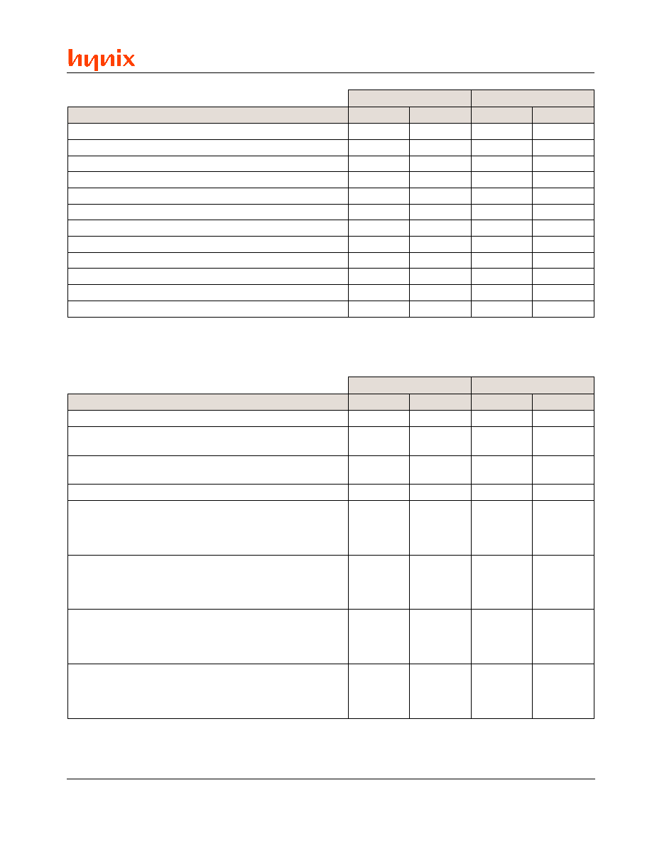
19
Rev. 1.2/May 01
HY29LV160
e
d
o
M
d
r
o
W
e
d
o
M
e
t
y
B
n
o
i
t
p
i
r
c
s
e
D
s
s
e
r
d
d
A
a
t
a
D
s
s
e
r
d
d
A
a
t
a
D
V
C
C
)
V
7
.
2
(
m
u
m
i
n
i
m
,
y
l
p
p
u
s
B
1
7
2
0
0
6
3
7
2
V
C
C
)
V
6
.
3
(
m
u
m
i
x
a
m
,
y
l
p
p
u
s
C
1
6
3
0
0
8
3
6
3
V
P
P
)
e
n
o
n
(
m
u
m
i
n
i
m
,
y
l
p
p
u
s
D
1
0
0
0
0
A
3
0
0
V
P
P
)
e
n
o
n
(
m
u
m
i
x
a
m
,
y
l
p
p
u
s
E
1
0
0
0
0
C
3
0
0
2
(
e
t
i
r
w
e
t
y
b
/
d
r
o
w
e
l
g
n
i
s
r
o
f
t
u
o
e
m
i
t
l
a
c
i
p
y
T
N
)
s
µ
F
1
4
0
0
0
E
3
4
0
2
(
e
t
i
r
w
r
e
f
f
u
b
e
z
i
s
m
u
m
i
x
a
m
r
o
f
t
u
o
e
m
i
t
l
a
c
i
p
y
T
N
)
s
µ
0
2
0
0
0
0
0
4
0
0
2
(
e
s
a
r
e
k
c
o
l
b
l
a
u
d
i
v
i
d
n
i
r
o
f
t
u
o
e
m
i
t
l
a
c
i
p
y
T
N
)
s
m
1
2
A
0
0
0
2
4
A
0
2
(
e
s
a
r
e
p
i
h
c
ll
u
f
r
o
f
t
u
o
e
m
i
t
l
a
c
i
p
y
T
N
)
s
m
2
2
F
0
0
0
4
4
F
0
2
(
e
t
i
r
w
e
t
y
b
/
d
r
o
w
e
l
g
n
i
s
r
o
f
t
u
o
e
m
i
t
m
u
m
i
x
a
M
N
)
p
y
T
x
3
2
5
0
0
0
6
4
5
0
2
(
e
t
i
r
w
r
e
f
f
u
b
e
z
i
s
m
u
m
i
x
a
m
r
o
f
t
u
o
e
m
i
t
m
u
m
i
x
a
M
N
)
p
y
T
x
4
2
0
0
0
0
8
4
0
0
2
(
e
s
a
r
e
k
c
o
l
b
l
a
u
d
i
v
i
d
n
i
r
o
f
t
u
o
e
m
i
t
m
u
m
i
x
a
M
N
)
p
y
T
x
5
2
4
0
0
0
A
4
3
0
)
d
e
t
r
o
p
p
u
s
t
o
n
(
e
s
a
r
e
p
i
h
c
ll
u
f
r
o
f
t
u
o
e
m
i
t
m
u
m
i
x
a
M
6
2
0
0
0
0
C
4
0
0
Table 8. CFI Mode: System Interface Data Values
e
d
o
M
d
r
o
W
e
d
o
M
e
t
y
B
n
o
i
t
p
i
r
c
s
e
D
s
s
e
r
d
d
A
a
t
a
D
s
s
e
r
d
d
A
a
t
a
D
2
(
e
z
i
s
e
c
i
v
e
D
N
)
s
e
t
y
b
7
2
5
1
0
0
E
4
5
1
e
d
o
c
e
c
a
f
r
e
t
n
i
e
c
i
v
e
d
h
s
a
l
F
)
6
1
x
/
8
x
s
u
o
n
o
r
h
c
n
y
s
a
=
2
0
(
8
2
9
2
2
0
0
0
0
0
0
0
0
5
2
5
2
0
0
0
t
o
n
(
e
t
i
r
w
e
t
y
b
-
i
t
l
u
m
n
i
s
e
t
y
b
f
o
r
e
b
m
u
n
m
u
m
i
x
a
M
)
d
e
t
r
o
p
p
u
s
A
2
B
2
0
0
0
0
0
0
0
0
4
5
6
5
0
0
0
0
s
n
o
i
g
e
r
k
c
o
l
b
e
s
a
r
e
f
o
r
e
b
m
u
N
C
2
4
0
0
0
8
5
4
0
n
o
i
t
a
m
r
o
f
n
i
1
n
o
i
g
e
r
k
c
o
l
b
e
s
a
r
E
1
-
n
o
i
g
e
r
n
i
s
k
c
o
l
b
f
o
#
=
]
D
2
,
E
2
[
s
e
t
y
b
-
6
5
2
f
o
s
e
l
p
i
t
l
u
m
n
i
e
z
i
s
=
]
F
2
,
0
3
[
D
2
E
2
F
2
0
3
0
0
0
0
0
0
0
0
0
4
0
0
0
0
0
0
A
5
C
5
E
5
0
6
0
0
0
0
0
4
0
0
n
o
i
t
a
m
r
o
f
n
i
2
n
o
i
g
e
r
k
c
o
l
b
e
s
a
r
E
1
3
2
3
3
3
4
3
1
0
0
0
0
0
0
0
0
2
0
0
0
0
0
0
2
6
4
6
6
6
8
6
1
0
0
0
0
2
0
0
n
o
i
t
a
m
r
o
f
n
i
3
n
o
i
g
e
r
k
c
o
l
b
e
s
a
r
E
5
3
6
3
7
3
8
3
0
0
0
0
0
0
0
0
0
8
0
0
0
0
0
0
A
6
C
6
E
6
0
7
0
0
0
0
0
8
0
0
n
o
i
t
a
m
r
o
f
n
i
4
n
o
i
g
e
r
k
c
o
l
b
e
s
a
r
E
9
3
A
3
B
3
C
3
E
1
0
0
0
0
0
0
0
0
0
0
1
0
0
0
2
7
4
7
6
7
8
7
E
1
0
0
0
0
1
0
Table 9. CFI Mode: Device Geometry Data Values
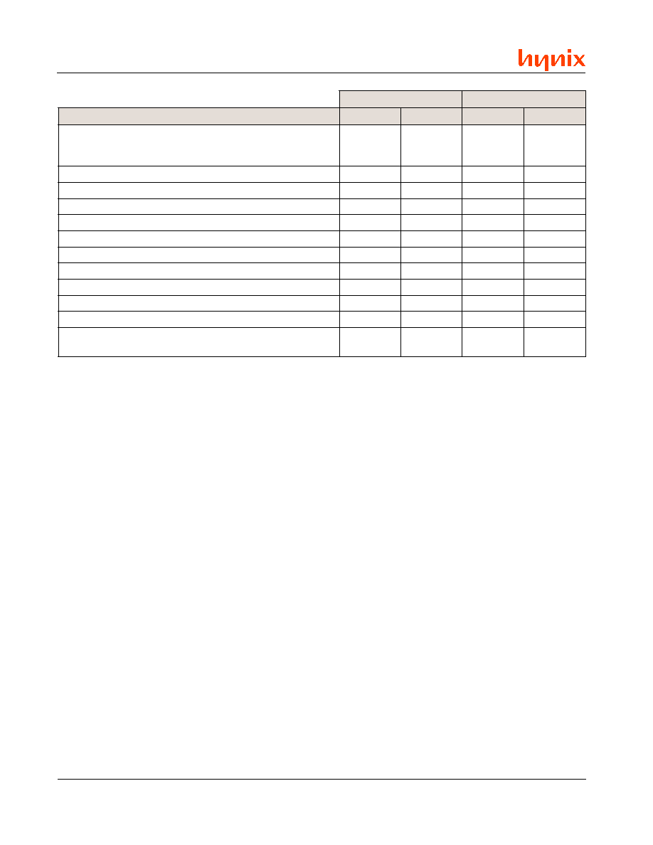
20
Rev. 1.2/May 01
HY29LV160
e
d
o
M
d
r
o
W
e
d
o
M
e
t
y
B
n
o
i
t
p
i
r
c
s
e
D
s
s
e
r
d
d
A
a
t
a
D
s
s
e
r
d
d
A
a
t
a
D
"
I
R
P
"
g
n
i
r
t
s
I
I
C
S
A
e
u
q
i
n
u
-
y
r
e
u
Q
0
4
1
4
2
4
0
5
0
0
2
5
0
0
9
4
0
0
0
8
2
8
4
8
0
5
2
5
9
4
I
I
C
S
A
,
r
e
b
m
u
n
n
o
i
s
r
e
v
r
o
j
a
M
3
4
1
3
0
0
6
8
1
3
I
I
C
S
A
,
r
e
b
m
u
n
n
o
i
s
r
e
v
r
o
n
i
M
4
4
0
3
0
0
8
8
0
3
k
c
o
l
n
u
e
v
i
t
i
s
n
e
s
s
s
e
r
d
d
A
)
d
e
r
i
u
q
e
r
t
o
n
=
1
,
d
e
r
i
u
q
e
r
=
0
(
5
4
0
0
0
0
A
8
0
0
d
n
e
p
s
u
s
e
s
a
r
E
e
t
i
r
w
d
n
a
d
a
e
r
o
t
=
2
(
)
6
4
2
0
0
0
C
8
2
0
t
c
e
t
o
r
p
r
o
t
c
e
S
)
p
u
o
r
g
/
s
r
o
t
c
e
s
f
o
#
=
N
(
7
4
1
0
0
0
E
8
1
0
t
c
e
t
o
r
p
n
u
r
o
t
c
e
s
y
r
a
r
o
p
m
e
T
)
d
e
t
r
o
p
p
u
s
=
1
(
8
4
1
0
0
0
0
9
1
0
e
m
e
h
c
s
t
c
e
t
o
r
p
n
u
/
t
c
e
t
o
r
p
r
o
t
c
e
S
)
d
o
h
t
e
m
A
0
0
8
V
L
9
2
m
A
=
4
(
9
4
4
0
0
0
2
9
4
0
n
o
i
t
a
r
e
p
o
W
/
R
s
u
o
e
n
a
t
l
u
m
i
S
)
d
e
t
r
o
p
p
u
s
t
o
n
=
0
(
A
4
0
0
0
0
4
9
0
0
e
p
y
t
e
d
o
m
t
s
r
u
B
)
d
e
t
r
o
p
p
u
s
t
o
n
=
0
(
B
4
0
0
0
0
6
9
0
0
e
p
y
t
e
d
o
m
e
g
a
P
)
d
e
t
r
o
p
p
u
s
t
o
n
=
0
(
C
4
0
0
0
0
8
9
0
0
n
o
i
s
r
e
v
t
o
o
b
m
o
t
t
o
b
/
p
o
T
)
t
o
o
B
p
o
T
=
B
T
,
t
o
o
B
m
o
t
t
o
B
=
B
B
(
D
4
)
B
B
(
2
0
0
0
)
B
T
(
3
0
0
0
A
9
)
B
B
(
2
0
)
B
T
(
3
0
Table 10. CFI Mode: Vendor-Specific Extended Query Data Values
WRITE OPERATION STATUS
The HY29LV160 provides a number of facilities to
determine the status of a program or erase op-
eration. These are the RY/BY# (Ready/Busy#)
pin and certain bits of a status word which can be
read from the device during the programming and
erase operations. Table 11 summarizes the sta-
tus indications and further detail is provided in the
subsections which follow.
RY/BY# - Ready/Busy#
RY/BY# is an open-drain output pin that indicates
whether a programming or erase Automatic Algo-
rithm is in progress or has completed. A pull-up
resistor to V
CC
is required for proper operation. RY/
BY# is valid after the rising edge of the final WE#
pulse in the corresponding command sequence.
If the output is Low (busy), the device is actively
erasing or programming, including programming
while in the Erase Suspend mode. If the output is
High (ready), the device has completed the op-
eration and is ready to read array data in the nor-
mal or Erase Suspend modes, or it is in the
Standby mode.
DQ[7] - Data# Polling
The Data# ("Data Bar") Polling bit, DQ[7], indicates
to the host system whether an Automatic Algo-
rithm is in progress or completed, or whether the
device is in Erase Suspend mode. Data# Polling
is valid after the rising edge of the final WE# pulse
in the Program or Erase command sequence.
The system must do a read at the program ad-
dress to obtain valid programming status informa-
tion on this bit. While a programming operation is
in progress, the device outputs the complement
of the value programmed to DQ[7]. When the pro-
gramming operation is complete, the device out-
puts the value programmed to DQ[7]. If a pro-
gram operation is attempted within a protected
sector, Data# Polling on DQ[7] is active for ap-
proximately 1 µs, then the device returns to read-
ing array data.
The host must read at an address within any non-
protected sector specified for erasure to obtain
valid erase status information on DQ[7]. During
an erase operation, Data# Polling produces a "0"
on DQ[7]. When the erase operation is complete,
or if the device enters the Erase Suspend mode,
Data# Polling produces a "1" on DQ[7]. If all sec-
tors selected for erasing are protected, Data#
Polling on DQ[7] is active for approximately 100
µs, then the device returns to reading array data.
If at least one selected sector is not protected, the
erase operation erases the unprotected sectors,
and ignores the command for the specified sec-
tors that are protected.
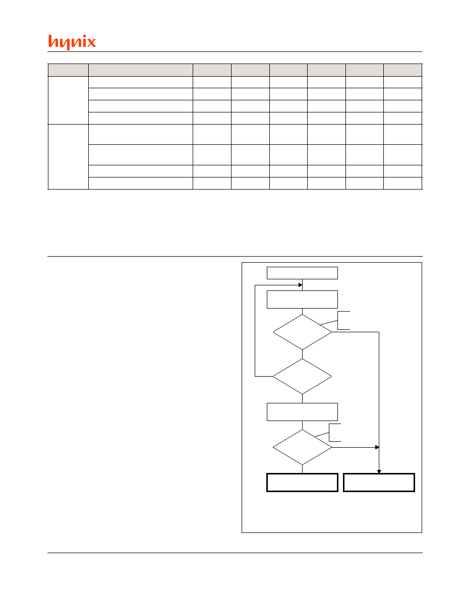
21
Rev. 1.2/May 01
HY29LV160
When the system detects that DQ[7] has changed
from the complement to true data (or "0" to "1" for
erase), it should do an additional read cycle to read
valid data from DQ[7:0]. This is because DQ[7]
may change asynchronously with respect to the
other data bits while Output Enable (OE#) is as-
serted low.
Figure 7 illustrates the Data# Polling test algorithm.
DQ[6] - Toggle Bit I
Toggle Bit I on DQ[6] indicates whether an Auto-
matic Program or Erase algorithm is in progress
or complete, or whether the device has entered
the Erase Suspend mode. Toggle Bit I may be
read at any address, and is valid after the rising
edge of the final WE# pulse in the Program or
Erase command sequence, including during the
sector erase time-out. The system may use ei-
ther OE# or CE# to control the read cycles.
Successive read cycles at any address during an
Automatic Program algorithm operation (including
programming while in Erase Suspend mode)
cause DQ[6] to toggle. DQ[6] stops toggling when
the operation is complete. If a program address
falls within a protected sector, DQ[6] toggles for
approximately 1 µs after the program command
sequence is written, then returns to reading array
data.
Table 11. Write and Erase Operation Status Summary
Notes:
1. A valid address is required when reading status information. See text for additional information.
2. DQ[5] status switches to a `1' when a program or erase operation exceeds the maximum timing limit.
3. A `1' during sector erase indicates that the 50 µs time-out has expired and active erasure is in progress. DQ[3] is not
applicable to the chip erase operation.
4. Equivalent to `No Toggle' because data is obtained in this state.
5. Data (DQ[7:0]) = 0xFF immediately after erasure.
6. Programming can be done only in a non-suspended sector (a sector not specified for erasure).
e
d
o
M
n
o
i
t
a
r
e
p
O
]
7
[
Q
D
1
]
6
[
Q
D
]
5
[
Q
D
]
3
[
Q
D
]
2
[
Q
D
1
#
Y
B
/
Y
R
l
a
m
r
o
N
s
s
e
r
g
o
r
p
n
i
g
n
i
m
m
a
r
g
o
r
P
#
]
7
[
Q
D
e
l
g
g
o
T
1
/
0
2
A
/
N
A
/
N
0
d
e
t
e
l
p
m
o
c
g
n
i
m
m
a
r
g
o
r
P
a
t
a
D
a
t
a
D
4
a
t
a
D
a
t
a
D
a
t
a
D
1
s
s
e
r
g
o
r
p
n
i
e
s
a
r
E
0
e
l
g
g
o
T
1
/
0
2
1
3
e
l
g
g
o
T
0
d
e
t
e
l
p
m
o
c
e
s
a
r
E
5
a
t
a
D
a
t
a
D
4
a
t
a
D
a
t
a
D
a
t
a
D
4
1
e
s
a
r
E
d
n
e
p
s
u
S
d
e
d
n
e
p
s
u
s
e
s
a
r
e
n
i
h
t
i
w
d
a
e
R
r
o
t
c
e
s
1
e
l
g
g
o
t
o
N
0
A
/
N
e
l
g
g
o
T
1
e
s
a
r
e
-
n
o
n
n
i
h
t
i
w
d
a
e
R
r
o
t
c
e
s
d
e
d
n
e
p
s
u
s
a
t
a
D
a
t
a
D
a
t
a
D
a
t
a
D
a
t
a
D
1
s
s
e
r
g
o
r
p
n
i
g
n
i
m
m
a
r
g
o
r
P
6
#
]
7
[
Q
D
e
l
g
g
o
T
1
/
0
2
A
/
N
A
/
N
0
d
e
t
e
l
p
m
o
c
g
n
i
m
m
a
r
g
o
r
P
6
a
t
a
D
a
t
a
D
4
a
t
a
D
a
t
a
D
a
t
a
D
1
START
Read DQ[7:0]
at Valid Address (Note 1)
DQ[7] = Data?
N O
YES
P R O G R A M / E R A S E
C O M P L E T E
DQ[5] = 1?
N O
YES
Test for DQ[7] = 1?
for Erase Operation
Read DQ[7:0]
at Valid Address (Note 1)
DQ[7] = Data?
(Note 2)
N O
YES
Test for DQ[7] = 1?
for Erase Operation
P R O G R A M / E R A S E
EXCEEDED TIME ERROR
Notes:
1. During programming , the program address. During sector erase , an
address within any non-protected sector specified for erasure. During
chip erase , an address within any non-protected sector.
2. Recheck DQ[7] since it may change asynchronously to DQ[5].
Figure 7. Data# Polling Test Algorithm
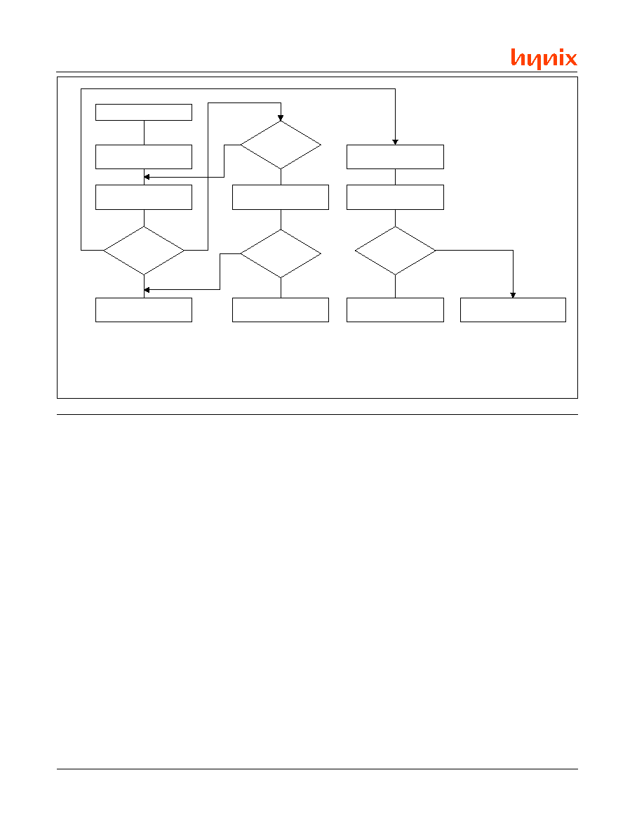
22
Rev. 1.2/May 01
HY29LV160
While the Automatic Erase algorithm is operating,
successive read cycles at any address cause
DQ[6] to toggle. DQ[6] stops toggling when the
erase operation is complete or when the device is
placed in the Erase Suspend mode. The host may
use DQ[2] to determine which sectors are erasing
or erase-suspended (see below). After an Erase
command sequence is written, if all sectors se-
lected for erasing are protected, DQ[6] toggles for
approximately 100 µs, then returns to reading ar-
ray data. If at least one selected sector is not
protected, the Automatic Erase algorithm erases
the unprotected sectors, and ignores the selected
sectors that are protected.
DQ[2] - Toggle Bit II
Toggle Bit II, DQ[2], when used with DQ[6], indi-
cates whether a particular sector is actively eras-
ing or whether that sector is erase-suspended.
Toggle Bit II is valid after the rising edge of the
final WE# pulse in the command sequence. The
device toggles DQ[2] with each OE# or CE# read
cycle.
Read DQ[7:0]
at Valid Address (Note 1)
DQ[6] Toggled?
N O
(Note 3)
Y E S
PROGRAM/ERASE
C O M P L E T E
DQ[5] = 1?
N O
Y E S
Read DQ[7:0]
at Valid Address (Note 1)
DQ[6] Toggled?
(Note 2)
N O
Y E S
PROGRAM/ERASE
EXCEEDED TIME ERROR
Notes:
1. During programming, the program address.
During sector erase, an address within any sector scheduled for erasure.
2. Recheck DQ[6] since toggling may stop at the same time as DQ[5] changes from 0 to 1.
3. Use this path if testing for Program/Erase status.
4. Use this path to test whether sector is in Erase Suspend mode.
Read DQ[7:0]
at Valid Address (Note 1)
START
Read DQ[7:0]
DQ[2] Toggled?
N O
SECTOR BEING READ
IS IN ERASE SUSPEND
Read DQ[7:0]
Y E S
N O
(Note 4)
SECTOR BEING READ
IS NOT IN ERASE SUSPEND
Figure 8. Toggle Bit I and II Test Algorithm
DQ[2] toggles when the host reads at addresses
within sectors that have been specified for era-
sure, but cannot distinguish whether the sector is
actively erasing or is erase-suspended. DQ[6],
by comparison, indicates whether the device is ac-
tively erasing or is in Erase Suspend, but cannot
distinguish which sectors are specified for erasure.
Thus, both status bits are required for sector and
mode information.
Figure 8 illustrates the operation of Toggle Bits I
and II.
DQ[5] - Exceeded Timing Limits
DQ[5] is set to a `1' when the program or erase
time has exceeded a specified internal pulse count
limit. This is a failure condition that indicates that
the program or erase cycle was not successfully
completed. DQ[5] status is valid only while DQ[7]
or DQ[6] indicate that the Automatic Algorithm is
in progress.
The DQ[5] failure condition will also be signaled if
the host tries to program a `1' to a location that is
previously programmed to `0', since only an erase
operation can change a `0' to a `1'.

23
Rev. 1.2/May 01
HY29LV160
For both of these conditions, the host must issue
a Reset command to return the device to the Read
mode.
DQ[3] - Sector Erase Timer
After writing a Sector Erase command sequence,
the host may read DQ[3] to determine whether or
not an erase operation has begun. When the
sector erase time-out expires and the sector erase
operation commences, DQ[3] switches from a `0'
to a `1'. Refer to the "Sector Erase Command"
section for additional information. Note that the
sector erase timer does not apply to the Chip Erase
command.
After the initial Sector Erase command sequence
is issued, the system should read the status on
DQ[7] (Data# Polling) or DQ[6] (Toggle Bit I) to
ensure that the device has accepted the command
sequence, and then read DQ[3]. If DQ[3] is a `1',
the internally controlled erase cycle has begun and
all further sector erase data cycles or commands
(other than Erase Suspend) are ignored until the
erase operation is complete. If DQ[3] is a `0', the
device will accept a sector erase data cycle to mark
an additional sector for erasure. To ensure that
the data cycles have been accepted, the system
software should check the status of DQ[3] prior to
and following each subsequent sector erase data
cycle. If DQ[3] is high on the second status check,
the last data cycle might not have been accepted.
HARDWARE DATA PROTECTION
The HY29LV160 provides several methods of pro-
tection to prevent accidental erasure or program-
ming which might otherwise be caused by spuri-
ous system level signals during V
CC
power-up and
power-down transitions, or from system noise.
These methods are described in the sections that
follow.
Command Sequences
Commands that may alter array data require a
sequence of cycles as described in Table 6. This
provides data protection against inadvertent writes.
Low V
CC
Write Inhibit
To protect data during V
CC
power-up and power-
down, the device does not accept write cycles
when V
CC
is less than V
LKO
(typically 2.4 volts). The
command register and all internal program/erase
circuits are disabled, and the device resets to the
Read mode. Writes are ignored until V
CC
is greater
than V
LKO
. The system must provide the proper
signals to the control pins to prevent unintentional
writes when V
CC
is greater than V
LKO
.
Write Pulse "Glitch" Protection
Noise pulses of less than 5 ns (typical) on OE#,
CE# or WE# do not initiate a write cycle.
Logical Inhibit
Write cycles are inhibited by asserting any one of
the following conditions: OE# = V
IL
, CE# = V
IH
, or
WE# = V
IH
. To initiate a write cycle, CE# and WE#
must be a logical zero while OE# is a logical one.
Power-Up Write Inhibit
If WE# = CE# = V
IL
and OE# = V
IH
during power
up, the device does not accept commands on the
rising edge of WE#. The internal state machine is
automatically reset to the Read mode on power-
up.
Sector Protection
Additional data protection is provided by the
HY29LV160's sector protect feature, described
previously, which can be used to protect sensitive
areas of the Flash array from accidental or unau-
thorized attempts to alter the data.
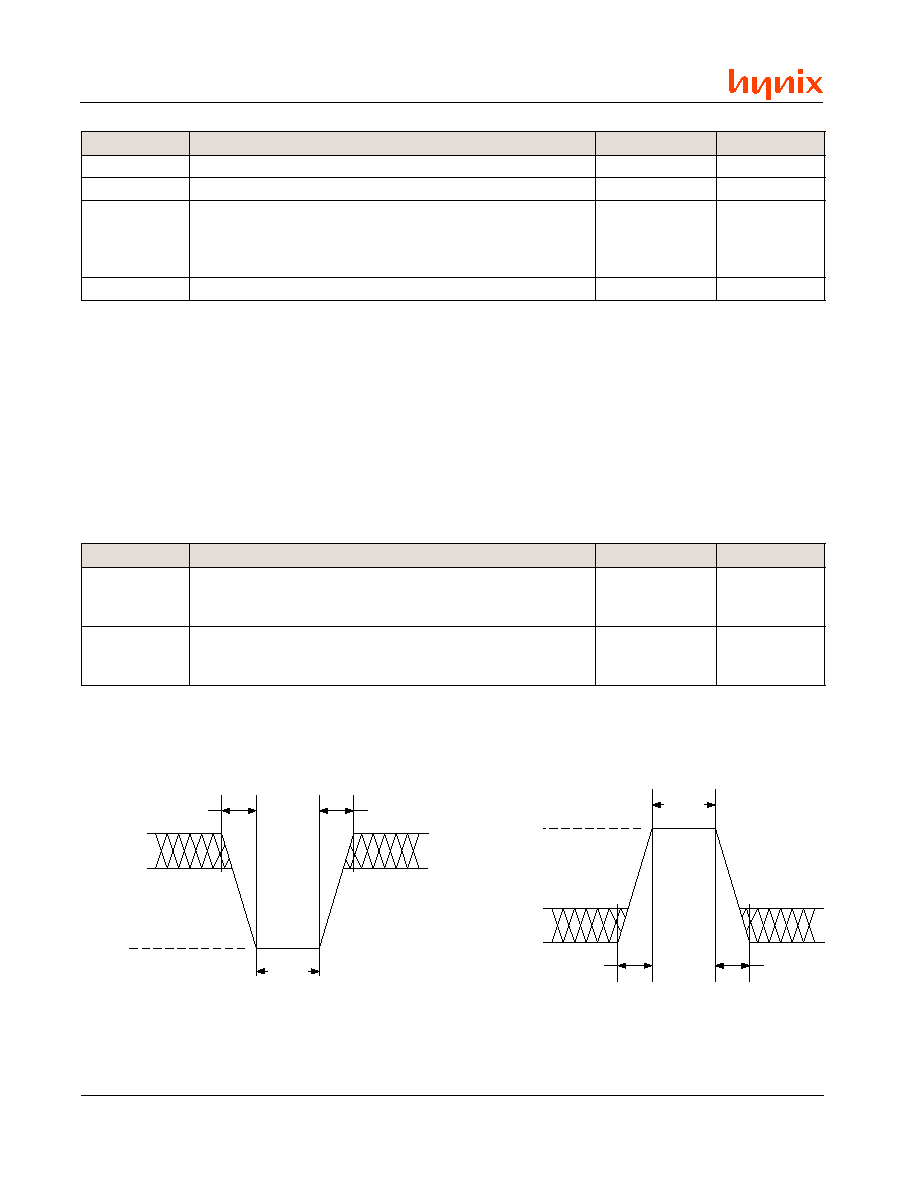
24
Rev. 1.2/May 01
HY29LV160
ABSOLUTE MAXIMUM RATINGS
4
l
o
b
m
y
S
r
e
t
e
m
a
r
a
P
e
u
l
a
V
t
i
n
U
T
G
T
S
e
r
u
t
a
r
e
p
m
e
T
e
g
a
r
o
t
S
0
5
1
+
o
t
5
6
-
C
∫
T
S
A
I
B
d
e
il
p
p
A
r
e
w
o
P
h
t
i
w
e
r
u
t
a
r
e
p
m
e
T
t
n
e
i
b
m
A
5
2
1
+
o
t
5
5
-
C
∫
V
2
N
I
V
o
t
t
c
e
p
s
e
R
h
t
i
w
n
i
P
n
o
e
g
a
t
l
o
V
S
S
:
C
C
V
1
#
T
E
S
E
R
,
#
E
O
,
]
9
[
A
2
s
n
i
P
r
e
h
t
O
ll
A
1
0
.
4
+
o
t
5
.
0
-
5
.
2
1
+
o
t
5
.
0
-
V
o
t
5
.
0
-
C
C
5
.
0
+
V
V
V
I
S
O
t
n
e
r
r
u
C
t
i
u
c
r
i
C
t
r
o
h
S
t
u
p
t
u
O
3
0
0
2
A
m
Notes:
1. Minimum DC voltage on input or I/O pins is ≠0.5 V. During voltage transitions, input or I/O pins may undershoot V
SS
to
-2.0V for periods of up to 20 ns. See Figure 9. Maximum DC voltage on input or I/O pins is V
CC
+ 0.5 V. During voltage
transitions, input or I/O pins may overshoot to V
CC
+2.0 V for periods up to 20 ns. See Figure 10.
2. Minimum DC input voltage on pins A[9], OE#, and RESET# is -0.5 V. During voltage transitions, A[9], OE#, and RESET#
may undershoot V
SS
to ≠2.0 V for periods of up to 20 ns. See Figure 9. Maximum DC input voltage on pin A[9] is +12.5
V which may overshoot to 14.0 V for periods up to 20 ns.
3. No more than one output at a time may be shorted to V
SS
. Duration of the short circuit should be less than one second.
4. Stresses above those listed under "Absolute Maximum Ratings" may cause permanent damage to the device. This is a
stress rating only; functional operation of the device at these or any other conditions above those indicated in the
operational sections of this data sheet is not implied. Exposure of the device to absolute maximum rating conditions for
extended periods may affect device reliability.
RECOMMENDED OPERATING CONDITIONS
1
l
o
b
m
y
S
r
e
t
e
m
a
r
a
P
e
u
l
a
V
t
i
n
U
T
A
:
e
r
u
t
a
r
e
p
m
e
T
g
n
i
t
a
r
e
p
O
t
n
e
i
b
m
A
s
e
c
i
v
e
D
e
r
u
t
a
r
e
p
m
e
T
l
a
i
c
r
e
m
m
o
C
s
e
c
i
v
e
D
e
r
u
t
a
r
e
p
m
e
T
l
a
i
r
t
s
u
d
n
I
0
7
+
o
t
0
5
8
+
o
t
0
4
-
C
∫
C
∫
V
C
C
:
e
g
a
t
l
o
V
y
l
p
p
u
S
g
n
i
t
a
r
e
p
O
s
n
o
i
s
r
e
V
V
2
1
-
d
n
a
V
0
9
-
,
0
7
-
s
n
o
i
s
r
e
V
r
e
h
t
O
ll
A
6
.
3
+
o
t
0
.
3
+
6
.
3
+
o
t
7
.
2
+
V
V
Notes:
1. Recommended Operating Conditions define those limits between which the functionality of the device is guaranteed.
2.0 V
V
C C
+ 0.5 V
V
C C
+ 2.0 V
20 ns
20 ns
20 ns
Figure 9. Maximum Undershoot Waveform
Figure 10. Maximum Overshoot Waveform
0.8 V
- 0.5 V
- 2.0 V
20 ns
20 ns
20 ns
25
Rev. 1.2/May 01
HY29LV160
DC CHARACTERISTICS
r
e
t
e
m
a
r
a
P
n
o
i
t
p
i
r
c
s
e
D
p
u
t
e
S
t
s
e
T
2
n
i
M
p
y
T
x
a
M
t
i
n
U
I
I
L
t
n
e
r
r
u
C
d
a
o
L
t
u
p
n
I
V
N
I
V
=
S
S
V
o
t
C
C
0
.
1
±
A
µ
I
T
I
L
t
n
e
r
r
u
C
d
a
o
L
t
u
p
n
I
]
9
[
A
V
5
.
2
1
=
]
9
[
A
5
3
A
µ
I
O
L
t
n
e
r
r
u
C
e
g
a
k
a
e
L
t
u
p
t
u
O
V
T
U
O
V
=
S
S
V
o
t
C
C
0
.
1
±
A
µ
I
1
C
C
V
C
C
t
n
e
r
r
u
C
d
a
e
R
e
v
i
t
c
A
1
V
=
#
E
C
L
I
,
V
=
#
E
O
H
I
,
e
d
o
M
e
t
y
B
z
H
M
5
9
6
1
A
m
z
H
M
1
2
4
A
m
V
=
#
E
C
L
I
,
V
=
#
E
O
H
I
,
e
d
o
M
d
r
o
W
z
H
M
5
9
6
1
A
m
z
H
M
1
2
4
A
m
I
2
C
C
V
C
C
t
n
e
r
r
u
C
e
t
i
r
W
e
v
i
t
c
A
4
,
3
V
=
#
E
C
L
I
,
V
=
#
E
O
H
I
0
3
0
5
A
m
I
3
C
C
V
C
C
p
e
e
D
d
e
ll
o
r
t
n
o
C
#
E
C
t
n
e
r
r
u
C
y
b
d
n
a
t
S
V
=
#
E
C
C
C
,
V
3
.
0
±
V
=
#
T
E
S
E
R
C
C
V
3
.
0
±
1
5
A
µ
I
4
C
C
V
C
C
p
e
e
D
d
e
ll
o
r
t
n
o
C
#
T
E
S
E
R
t
n
e
r
r
u
C
y
b
d
n
a
t
S
V
=
#
T
E
S
E
R
S
S
V
3
.
0
±
1
5
A
µ
I
5
C
C
e
d
o
M
p
e
e
l
S
c
i
t
a
m
o
t
u
A
t
n
e
r
r
u
C
,
5
V
H
I
V
=
C
C
,
V
3
.
0
±
V
L
I
V
=
S
S
V
3
.
0
±
1
5
A
µ
I
6
C
C
V
C
C
l
a
m
r
o
N
d
e
ll
o
r
t
n
o
C
#
E
C
t
n
e
r
r
u
C
y
b
d
n
a
t
S
2
V
=
#
T
E
S
E
R
=
#
E
C
H
I
1
A
m
I
7
C
C
V
C
C
d
e
ll
o
r
t
n
o
C
#
T
E
S
E
R
t
n
e
r
r
u
C
y
b
d
n
a
t
S
l
a
m
r
o
N
2
V
=
#
T
E
S
E
R
L
I
1
A
m
V
L
I
e
g
a
t
l
o
V
w
o
L
t
u
p
n
I
5
.
0
-
8
.
0
V
V
H
I
e
g
a
t
l
o
V
h
g
i
H
t
u
p
n
I
x
7
.
0
V
C
C
V
C
C
3
.
0
+
V
V
D
I
d
n
a
D
I
c
i
n
o
r
t
c
e
l
E
r
o
f
e
g
a
t
l
o
V
t
c
e
t
o
r
p
n
U
r
o
t
c
e
S
y
r
a
r
o
p
m
e
T
V
C
C
V
3
.
3
=
5
.
1
1
5
.
2
1
V
V
L
O
e
g
a
t
l
o
V
w
o
L
t
u
p
t
u
O
V
C
C
V
=
C
C
,
n
i
M
I
L
O
A
m
0
.
4
=
5
4
.
0
V
V
1
H
O
e
g
a
t
l
o
V
h
g
i
H
t
u
p
t
u
O
V
C
C
V
=
C
C
,
n
i
M
I
H
O
A
m
0
.
2
-
=
x
5
8
.
0
V
C
C
V
V
2
H
O
V
C
C
V
=
C
C
,
n
i
M
I
H
O
0
0
1
-
=
A
µ
V
C
C
4
.
0
-
V
V
O
K
L
V
w
o
L
C
C
e
g
a
t
l
o
V
t
u
o
k
c
o
L
4
3
.
2
5
.
2
V
Notes:
1. The I
CC
current is listed is typically less than 2 mA/MHz with OE# at V
IH
. Typical V
CC
is 3.0 V.
2. All specifications are tested with V
CC
= V
CC
Max unless otherwise noted.
3. I
CC
active while the Automatic Erase or Automatic Program algorithm is in progress.
4. Not 100% tested.
5. Automatic sleep mode is enabled when addresses remain stable for t
ACC
+ 30 ns (typical).
26
Rev. 1.2/May 01
HY29LV160
0
500
1000
1500
2000
2500
3000
3500
4000
0
5
10
15
20
Time in ns
Supply Current in mA
DC CHARACTERISTICS
Zero Power Flash
Figure 11. I
CC1
Current vs. Time (Showing Active and Automatic Sleep Currents)
Note: Addresses are switching at 1 MHz.
Figure 12. Typical I
CC1
Current vs. Frequency
Note: T = 25 ∞C.
1
2
3
4
5
6
0
2
4
6
1 0
Frequency in MHz
Supply Current in mA
8
2.7 V
3.6 V
27
Rev. 1.2/May 01
HY29LV160
TEST CONDITIONS
Table 12. Test Specifications
Figure 13. Test Setup
Measurement Level
1.5 V Output
Input 1.5 V
0.0 V
3.0 V
Figure 14. Input Waveforms and Measurement Levels
t
s
e
T
n
o
i
t
i
d
n
o
C
0
7
-
0
8
-
0
9
-
2
1
-
t
i
n
U
d
a
o
L
t
u
p
t
u
O
e
t
a
G
L
T
T
1
C
(
e
c
n
a
t
i
c
a
p
a
C
d
a
o
L
t
u
p
t
u
O
L
)
0
3
0
0
1
F
p
s
e
m
i
T
ll
a
F
d
n
a
e
s
i
R
t
u
p
n
I
5
s
n
l
e
v
e
L
w
o
L
l
a
n
g
i
S
t
u
p
n
I
0
.
0
V
l
e
v
e
L
h
g
i
H
l
a
n
g
i
S
t
u
p
n
I
0
.
3
V
t
n
e
m
e
r
u
s
a
e
M
g
n
i
m
i
T
w
o
L
l
e
v
e
L
l
a
n
g
i
S
5
.
1
V
t
n
e
m
e
r
u
s
a
e
M
g
n
i
m
i
T
h
g
i
H
l
e
v
e
L
l
a
n
g
i
S
5
.
1
V
6.2
K O h m
C
L
2.7
K O h m
+ 3.3V
D E V I C E
U N D E R
T E S T
All diodes
are
1 N 3 0 6 4
or
equivalent
M
R
O
F
E
V
A
W
S
T
U
P
N
I
S
T
U
P
T
U
O
y
d
a
e
t
S
L
o
t
H
m
o
r
f
g
n
i
g
n
a
h
C
H
o
t
L
m
o
r
f
g
n
i
g
n
a
h
C
d
e
t
t
i
m
r
e
P
e
g
n
a
h
C
y
n
A
,
e
r
a
C
t
'
n
o
D
n
w
o
n
k
n
U
e
t
a
t
S
,
g
n
i
g
n
a
h
C
y
l
p
p
A
t
o
N
s
e
o
D
e
t
a
t
S
e
c
n
a
d
e
p
m
I
h
g
i
H
s
i
e
n
il
r
e
t
n
e
C
)
Z
h
g
i
H
(
KEY TO SWITCHING WAVEFORMS
Note: Timing measurements are made at the reference
levels specified above regardless of where the illustrations
in the timing diagrams appear to indicate the measurement
is made
28
Rev. 1.2/May 01
HY29LV160
AC CHARACTERISTICS
Read Operations
Notes:
1. Not 100% tested.
2. See Figure 13 and Table 12 for test conditions.
Addresses Stable
t
R C
t
A C C
Output Valid
t
O E
t
C E
t
O E H
t
O H
t
D F
RY/BY#
0 V
R E S E T #
Outputs
W E #
O E #
C E #
Addresses
Figure 15. Read Operation Timings
r
e
t
e
m
a
r
a
P
n
o
i
t
p
i
r
c
s
e
D
p
u
t
e
S
t
s
e
T
n
o
i
t
p
O
d
e
e
p
S
t
i
n
U
C
E
D
E
J
d
t
S
0
7
-
0
8
-
0
9
-
2
1
-
t
V
A
V
A
t
C
R
e
m
i
T
e
l
c
y
C
d
a
e
R
1
n
i
M
0
7
0
8
0
9
0
2
1
s
n
t
V
Q
V
A
t
C
C
A
y
a
l
e
D
t
u
p
t
u
O
o
t
s
s
e
r
d
d
A
V
=
#
E
C
L
I
V
=
#
E
O
L
I
x
a
M
0
7
0
8
0
9
0
2
1
s
n
t
V
Q
L
E
t
E
C
y
a
l
e
D
t
u
p
t
u
O
o
t
e
l
b
a
n
E
p
i
h
C
V
=
#
E
O
L
I
x
a
M
0
7
0
8
0
9
0
2
1
s
n
t
Z
Q
H
E
t
F
D
Z
h
g
i
H
t
u
p
t
u
O
o
t
e
l
b
a
n
E
p
i
h
C
1
x
a
M
5
2
5
2
0
3
0
3
s
n
t
V
Q
L
G
t
E
O
y
a
l
e
D
t
u
p
t
u
O
o
t
e
l
b
a
n
E
t
u
p
t
u
O
V
=
#
E
C
L
I
x
a
M
0
3
0
3
5
3
0
5
s
n
t
Z
Q
H
G
t
F
D
Z
h
g
i
H
t
u
p
t
u
O
o
t
e
l
b
a
n
E
t
u
p
t
u
O
1
x
a
M
5
2
5
2
0
3
0
3
s
n
t
H
E
O
e
l
b
a
n
E
t
u
p
t
u
O
e
m
i
T
d
l
o
H
1
d
a
e
R
n
i
M
0
s
n
d
n
a
e
l
g
g
o
T
g
n
il
l
o
P
#
a
t
a
D
n
i
M
0
1
s
n
t
X
Q
X
A
t
H
O
#
E
C
,
s
e
s
s
e
r
d
d
A
m
o
r
f
e
m
i
T
d
l
o
H
t
u
p
t
u
O
t
s
r
i
F
s
r
u
c
c
O
r
e
v
e
h
c
i
h
W
,
#
E
O
r
o
1
n
i
M
0
s
n
29
Rev. 1.2/May 01
HY29LV160
AC CHARACTERISTICS
Hardware Reset (RESET#)
Notes:
1. Not 100% tested.
2. See Figure 13 and Table 12 for test conditions.
Figure 16. RESET# Timings
Reset Timings NOT During Automatic Algorithms
Reset Timings During Automatic Algorithms
R Y / B Y #
0 V
t
R P
t
Ready
C E # , O E #
R E S E T #
t
R H
R Y / B Y #
t
R P
t
Ready
C E # , O E #
R E S E T #
t
R B
r
e
t
e
m
a
r
a
P
n
o
i
t
p
i
r
c
s
e
D
p
u
t
e
S
t
s
e
T
n
o
i
t
p
O
d
e
e
p
S
t
i
n
U
C
E
D
E
J
d
t
S
0
7
-
0
8
-
0
9
-
2
1
-
t
Y
D
A
E
R
c
i
t
a
m
o
t
u
A
g
n
i
r
u
D
(
w
o
L
n
i
P
#
T
E
S
E
R
e
t
i
r
W
r
o
d
a
e
R
o
t
)
s
m
h
t
i
r
o
g
l
A
1
x
a
M
0
2
s
µ
t
Y
D
A
E
R
c
i
t
a
m
o
t
u
A
g
n
i
r
u
D
T
O
N
(
w
o
L
n
i
P
#
T
E
S
E
R
e
t
i
r
W
r
o
d
a
e
R
o
t
)
s
m
h
t
i
r
o
g
l
A
1
x
a
M
0
0
5
s
n
t
P
R
h
t
d
i
W
e
s
l
u
P
#
T
E
S
E
R
n
i
M
0
0
5
s
n
t
H
R
d
a
e
R
e
r
o
f
e
B
e
m
i
T
h
g
i
H
#
T
E
S
E
R
1
n
i
M
0
5
s
n
t
D
P
R
e
d
o
M
y
b
d
n
a
t
S
o
t
w
o
L
#
T
E
S
E
R
x
a
M
0
2
s
µ
t
B
R
e
m
i
T
y
r
e
v
o
c
e
R
#
Y
B
/
Y
R
n
i
M
0
s
n
30
Rev. 1.2/May 01
HY29LV160
AC CHARACTERISTICS
Word/Byte Configuration (BYTE#)
r
e
t
e
m
a
r
a
P
n
o
i
t
p
i
r
c
s
e
D
n
o
i
t
p
O
d
e
e
p
S
t
i
n
U
C
E
D
E
J
d
t
S
0
7
-
0
8
-
0
9
-
2
1
-
t
L
F
L
E
w
o
L
g
n
i
h
c
t
i
w
S
#
E
T
Y
B
o
t
#
E
C
x
a
M
5
s
n
t
H
F
L
E
h
g
i
H
g
n
i
h
c
t
i
w
S
#
E
T
Y
B
o
t
#
E
C
x
a
M
5
s
n
t
Z
Q
L
F
Z
-
h
g
i
H
t
u
p
t
u
O
o
t
w
o
L
g
n
i
h
c
t
i
w
S
#
E
T
Y
B
x
a
M
5
2
5
2
0
3
0
3
s
n
t
V
Q
H
F
e
v
i
t
c
A
t
u
p
t
u
O
o
t
h
g
i
H
g
n
i
h
c
t
i
w
S
#
E
T
Y
B
n
i
M
0
7
0
8
0
9
0
2
1
s
n
Data Output DQ[14:0]
Data Output DQ[7:0]
Data Output DQ[7:0]
Data Output DQ[14:0]
Output DQ[15]
Address Input A-1
Address Input A-1
Data Output DQ[15]
t
E L F L
t
E L F H
t
F H Q V
t
F L Q Z
C E #
O E #
B Y T E #
DQ[14:0]
DQ[15]/A-1
B Y T E #
DQ[14:0]
DQ[15]/A-1
B Y T E #
switching
from word to
byte mode
B Y T E #
switching
from byte to
word mode
Figure 17. BYTE# Timings for Read Operations
Figure 18. BYTE# Timings for Write Operations
t
S E T
(t
A S
)
t
H O L D
(t
A H
)
Falling edge of the last WE# signal
C E #
W E #
B Y T E #
Note: Refer to the Program/Erase Operations table for t
AS
and t
AH
specifications.
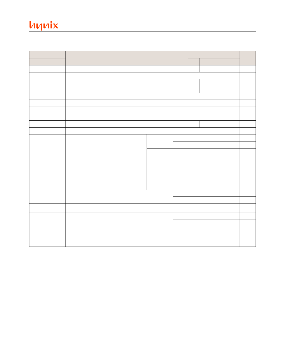
31
Rev. 1.2/May 01
HY29LV160
AC CHARACTERISTICS
Program and Erase Operations
Notes:
1. Not 100% tested.
2. Typical program and erase times assume the following conditions: 25 ∞C, V
CC
= 3.0 volts, 100,000 cycles. In addition,
programming typicals assume a checkerboard pattern. Maximum program and erase times are under worst case condi-
tions of 90 ∞C, V
CC
= 2.7 volts (3.0 volts for - 70 version), 100,000 cycles.
3. Excludes system-level overhead, which is the time required to execute the four-bus-cycle sequence for the program
command. See Table 6 for further information on command sequences.
4. Excludes 0x00 programming prior to erasure. In the preprogramming step of the Automatic Erase algorithm, all bytes
are programmed to 0x00 before erasure.
5. The typical chip programming time is considerably less than the maximum chip programming time listed since most
bytes/words program faster than the maximum programming times specified. The device sets DQ[5] = 1 only If the
maximum byte/word program time specified is exceeded. See Write Operation Status section for additional information.
r
e
t
e
m
a
r
a
P
n
o
i
t
p
i
r
c
s
e
D
n
o
i
t
p
O
d
e
e
p
S
t
i
n
U
C
E
D
E
J
d
t
S
0
7
-
0
8
-
0
9
-
2
1
-
t
V
A
V
A
t
C
W
e
m
i
T
e
l
c
y
C
e
t
i
r
W
1
n
i
M
0
7
0
8
0
9
0
2
1
s
n
t
L
W
V
A
t
S
A
e
m
i
T
p
u
t
e
S
s
s
e
r
d
d
A
n
i
M
0
s
n
t
X
A
L
W
t
H
A
e
m
i
T
d
l
o
H
s
s
e
r
d
d
A
n
i
M
5
4
5
4
5
4
0
5
s
n
t
H
W
V
D
t
S
D
e
m
i
T
p
u
t
e
S
a
t
a
D
n
i
M
5
3
5
3
5
4
0
5
s
n
t
X
D
H
W
t
H
D
e
m
i
T
d
l
o
H
a
t
a
D
n
i
M
0
s
n
t
L
W
H
G
t
L
W
H
G
e
t
i
r
W
e
r
o
f
e
B
e
m
i
T
y
r
e
v
o
c
e
R
d
a
e
R
n
i
M
0
s
n
t
L
W
L
E
t
S
C
e
m
i
T
p
u
t
e
S
#
E
C
n
i
M
0
s
n
t
H
E
H
W
t
H
C
e
m
i
T
d
l
o
H
#
E
C
n
i
M
0
s
n
t
H
W
L
W
t
P
W
h
t
d
i
W
e
s
l
u
P
e
t
i
r
W
n
i
M
5
3
5
3
5
3
0
5
s
n
t
L
W
H
W
t
H
P
W
h
g
i
H
h
t
d
i
W
e
s
l
u
P
e
t
i
r
W
n
i
M
0
3
s
n
t
1
H
W
H
W
t
1
H
W
H
W
n
o
i
t
a
r
e
p
O
g
n
i
m
m
a
r
g
o
r
P
3
,
2
,
1
e
d
o
M
e
t
y
B
p
y
T
9
s
µ
x
a
M
0
0
3
s
µ
e
d
o
M
d
r
o
W
p
y
T
8
1
s
µ
x
a
M
0
0
5
s
µ
n
o
i
t
a
r
e
p
O
g
n
i
m
m
a
r
g
o
r
P
p
i
h
C
5
,
3
,
2
,
1
e
d
o
M
e
t
y
B
p
y
T
8
1
c
e
s
x
a
M
4
5
c
e
s
e
d
o
M
d
r
o
W
p
y
T
8
1
c
e
s
x
a
M
4
5
c
e
s
t
2
H
W
H
W
t
2
H
W
H
W
n
o
i
t
a
r
e
p
O
e
s
a
r
E
r
o
t
c
e
S
4
,
2
,
1
p
y
T
5
2
.
0
c
e
s
x
a
M
5
c
e
s
t
3
H
W
H
W
t
3
H
W
H
W
n
o
i
t
a
r
e
p
O
e
s
a
r
E
p
i
h
C
4
,
2
,
1
p
y
T
8
c
e
s
e
c
n
a
r
u
d
n
E
e
l
c
y
C
m
a
r
g
o
r
P
d
n
a
e
s
a
r
E
1
p
y
T
0
0
0
,
0
0
0
,
1
s
e
l
c
y
c
n
i
M
0
0
0
,
0
0
1
s
e
l
c
y
c
t
S
C
V
V
C
C
e
m
i
T
p
u
t
e
S
1
n
i
M
0
5
s
µ
t
B
R
#
Y
B
/
Y
R
m
o
r
f
e
m
i
T
y
r
e
v
o
c
e
R
n
i
M
0
s
n
t
Y
S
U
B
y
a
l
e
D
#
Y
B
/
Y
R
o
t
h
g
i
H
#
E
W
n
i
M
0
9
s
n
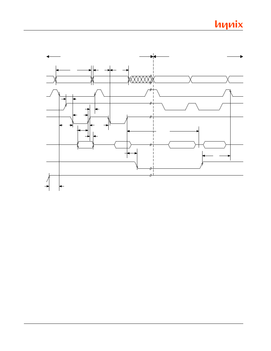
32
Rev. 1.2/May 01
HY29LV160
AC CHARACTERISTICS
Notes:
1. PA = Program Address, PD = Program Data, D
OUT
is the true data at the program address.
2. Commands shown are for Word mode operation.
3. V
CC
shown only to illustrate t
VCS
measurement references. It cannot occur as shown during a valid command sequence.
Figure 19. Program Operation Timings
Addresses
C E #
t
W C
0x555
P A
P A
PA
O E #
t
A S
t
A H
t
W P H
t
W P
t
G H W L
t
C S
W E #
Data
t
D S
t
D H
0xA0
P D
Status
t
W H W H 1
RY/BY#
t
B U S Y
t
R B
t
V C S
V
C C
Program Command Sequence (last two cycles)
Read Status Data (last two cycles)
D
O U T
t
C H
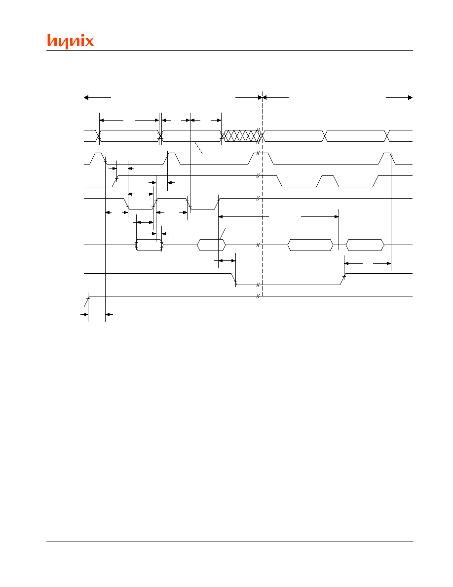
33
Rev. 1.2/May 01
HY29LV160
AC CHARACTERISTICS
Notes:
1. SA =Sector Address (for sector erase), VA = Valid Address for reading status data (see Write Operation Status section),
D
OUT
is the true data at the read address.(0xFF after an erase operation).
2. Commands shown are for Word mode operation.
3. V
CC
shown only to illustrate t
VCS
measurement references. It cannot occur as shown during a valid command sequence.
Figure 20. Sector/Chip Erase Operation Timings
Addresses
C E #
t
W C
0 x 2 A A
V A
V A
SA
O E #
t
A S
t
A H
t
W P H
t
W P
t
G H W L
t
C S
t
C H
W E #
Data
t
D S
t
D H
0x55
0x30
Status
D
O U T
t
W H W H 2
or
t
W H W H 3
RY/BY#
t
B U S Y
t
R B
t
V C S
V
C C
Erase Command Sequence (last two cycles)
Read Status Data (last two cycles)
Address = 0x555
for chip erase
Data = 0x10
for chip erase
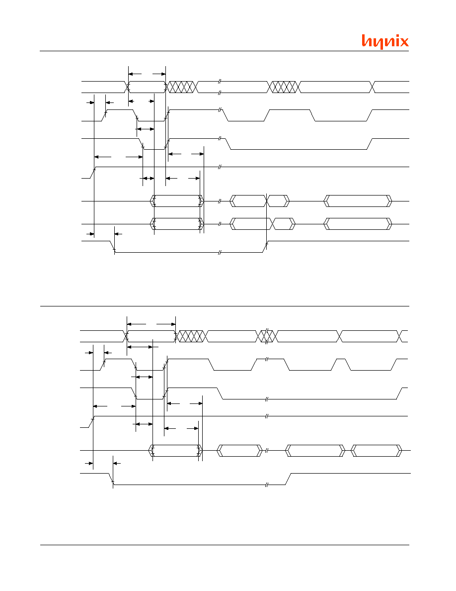
34
Rev. 1.2/May 01
HY29LV160
AC CHARACTERISTICS
Notes:
1. VA = Valid Address for reading Toggle Bits (DQ[2], DQ[6]) status data (see Write Operation Status section).
2. Illustration shows first two status read cycles after command sequence, last status read cycle and array data read cycle.
Figure 22. Toggle Polling Timings (During Automatic Algorithms)
t
B U S Y
t
C H
t
O E
t
C E
t
R C
C o m p l e m e n t
C o m p l e m e n t
T r u e
Valid Data
Status Data
Status Data
D a t a
Valid Data
RY/BY#
DQ[6:0]
DQ[7]
W E #
O E #
C E #
Addresses
V A
V A
V A
t
A C C
t
O E H
t
O H
t
D F
Notes:
1. VA = Valid Address for reading Data# Polling status data (see Write Operation Status section).
2. Illustration shows first status cycle after command sequence, last status read cycle and array data read cycle.
Figure 21. Data# Polling Timings (During Automatic Algorithms)
t
B U S Y
t
C H
t
O E
t
C E
t
R C
Valid Status
Valid Status
Valid Status
RY/BY#
DQ[6], [2]
W E #
O E #
C E #
Addresses
V A
V A
V A
t
O E H
t
O H
t
D F
V A
(second read)
(first read)
(stops toggling)
Valid Data
t
A C C
35
Rev. 1.2/May 01
HY29LV160
AC CHARACTERISTICS
Notes:
1. The system may use CE# or OE# to toggle DQ[2] and DQ[6]. DQ[2] toggles only when read at an address within an
erase-suspended sector.
Figure 23. DQ[2] and DQ[6] Operation
r
e
t
e
m
a
r
a
P
n
o
i
t
p
i
r
c
s
e
D
n
o
i
t
p
O
d
e
e
p
S
t
i
n
U
C
E
D
E
J
d
t
S
0
7
-
0
8
-
0
9
-
2
1
-
t
R
D
I
V
V
D
I
t
c
e
t
o
r
p
n
U
r
o
t
c
e
S
y
r
a
r
o
p
m
e
T
r
o
f
e
m
i
T
n
o
i
t
i
s
n
a
r
T
1
n
i
M
0
0
5
s
n
t
P
S
R
r
o
f
e
m
i
T
p
u
t
e
S
#
T
E
S
E
R
t
c
e
t
o
r
p
n
U
r
o
t
c
e
S
y
r
a
r
o
p
m
e
T
n
i
M
4
s
µ
t
T
S
R
V
t
c
e
t
o
r
P
r
o
t
c
e
S
m
e
t
s
y
S
-
n
I
r
o
f
e
m
i
T
p
u
t
e
S
#
T
E
S
E
R
t
c
e
t
o
r
p
n
U
d
n
a
n
i
M
1
s
µ
t
T
O
R
P
e
m
i
T
t
c
e
t
o
r
P
r
o
t
c
e
S
m
e
t
s
y
S
-
n
I
x
a
M
0
5
1
s
µ
t
R
P
N
U
e
m
i
T
t
c
e
t
o
r
p
n
U
r
o
t
c
e
S
m
e
t
s
y
S
-
n
I
x
a
M
5
1
s
m
In-System Sector Protect and Unprotect, Temporary Sector Unprotect
Notes:
1. Not 100% tested.
Figure 24. Temporary Sector Unprotect Timings
E r a s e
C o m p l e t e
W E #
DQ[6]
DQ[2]
Enter Automatic
E r a s e
E r a s e
E r a s e
S u s p e n d
R e a d
Enter Erase
S u s p e n d
P r o g r a m
E r a s e
S u s p e n d
P r o g r a m
E r a s e
S u s p e n d
R e a d
E r a s e
R e s u m e
E r a s e
E r a s e
S u s p e n d
t
V I D R
RY/BY#
W E #
C E #
R E S E T #
V
ID
0 or 3V
t
R S P
t
V I D R
0 or 3V
36
Rev. 1.2/May 01
HY29LV160
V
ID
V
IH
R E S E T #
Don't Care
Valid *
Valid *
Valid *
SA, A[6],
A[1], A[0]
0x60
0x60
0x40
Status
Data
C E #
W E #
O E #
t
V R E S
t
P R O T
Sector Protect/Unprotect
Verify
t
U N P R
Note: For Sector Protect, A[6] = 0, A[1] = 1, A[0] = 0. For Sector Unprotect, A[6] = 1, A[1] = 1, A[0] = 0.
Figure 25. In-System Sector Protect and Unprotect Timings
AC CHARACTERISTICS
37
Rev. 1.2/May 01
HY29LV160
AC CHARACTERISTICS
Alternate CE# Controlled Erase/Program Operations
Notes:
1. Not 100% tested.
2. Typical program and erase times assume the following conditions: 25 ∞C, V
CC
= 3.0 volts, 100,000 cycles. In addition,
programming typicals assume a checkerboard pattern. Maximum program and erase times are under worst case condi-
tions of 90 ∞C, V
CC
= 2.7 volts (3.0 volts for 70 ns version), 100,000 cycles.
3. Excludes system-level overhead, which is the time required to execute the four-bus-cycle sequence for the program
command. See Table 6 for further information on command sequences.
4. Excludes 0x00 programming prior to erasure. In the preprogramming step of the Automatic Erase algorithm, all bytes
are programmed to 0x00 before erasure.
5. The typical chip programming time is considerably less than the maximum chip programming time listed since most
bytes program faster than the maximum programming times specified. The device sets DQ[5] = 1 only If the maximum
byte program time specified is exceeded. See Write Operation Status section for additional information.
r
e
t
e
m
a
r
a
P
n
o
i
t
p
i
r
c
s
e
D
n
o
i
t
p
O
d
e
e
p
S
t
i
n
U
C
E
D
E
J
d
t
S
0
7
-
0
8
-
0
9
-
2
1
-
t
V
A
V
A
t
C
W
e
m
i
T
e
l
c
y
C
e
ti
r
W
1
n
i
M
0
7
0
8
0
9
0
2
1
s
n
t
L
E
V
A
t
S
A
e
m
i
T
p
u
t
e
S
s
s
e
r
d
d
A
n
i
M
0
s
n
t
X
A
L
E
t
H
A
e
m
i
T
d
l
o
H
s
s
e
r
d
d
A
n
i
M
5
4
5
4
5
4
0
5
s
n
t
H
E
V
D
t
S
D
e
m
i
T
p
u
t
e
S
a
t
a
D
n
i
M
5
3
5
3
5
4
0
5
s
n
t
X
D
H
E
t
H
D
e
m
i
T
d
l
o
H
a
t
a
D
n
i
M
0
s
n
t
L
E
H
G
t
L
E
H
G
e
ti
r
W
e
r
o
f
e
B
e
m
i
T
y
r
e
v
o
c
e
R
d
a
e
R
n
i
M
0
s
n
t
L
E
L
W
t
S
W
e
m
i
T
p
u
t
e
S
#
E
W
n
i
M
0
s
n
t
H
W
H
E
t
H
W
e
m
i
T
d
l
o
H
#
E
W
n
i
M
0
s
n
t
H
E
L
E
t
P
C
h
t
d
i
W
e
s
l
u
P
#
E
C
n
i
M
5
3
5
3
5
3
0
5
s
n
t
L
E
H
E
t
H
P
C
h
g
i
H
h
t
d
i
W
e
s
l
u
P
#
E
C
n
i
M
0
3
s
n
t
1
H
W
H
W
t
1
H
W
H
W
n
o
i
t
a
r
e
p
O
g
n
i
m
m
a
r
g
o
r
P
3
,
2
,
1
e
d
o
M
e
t
y
B
p
y
T
9
s
µ
x
a
M
0
0
3
s
µ
d
r
o
W
e
d
o
M
p
y
T
8
1
s
µ
x
a
M
0
0
5
s
µ
n
o
i
t
a
r
e
p
O
g
n
i
m
m
a
r
g
o
r
P
p
i
h
C
5
,
3
,
2
,
1
e
d
o
M
e
t
y
B
p
y
T
8
1
c
e
s
x
a
M
4
5
c
e
s
d
r
o
W
e
d
o
M
p
y
T
8
1
c
e
s
x
a
M
4
5
c
e
s
t
2
H
W
H
W
t
2
H
W
H
W
n
o
i
t
a
r
e
p
O
e
s
a
r
E
r
o
t
c
e
S
4
,
2
,
1
p
y
T
5
2
.
0
c
e
s
x
a
M
5
c
e
s
t
3
H
W
H
W
t
3
H
W
H
W
n
o
i
t
a
r
e
p
O
e
s
a
r
E
p
i
h
C
4
,
2
,
1
p
y
T
8
c
e
s
e
c
n
a
r
u
d
n
E
e
l
c
y
C
m
a
r
g
o
r
P
d
n
a
e
s
a
r
E
1
p
y
T
0
0
0
,
0
0
0
,
1
s
e
l
c
y
c
n
i
M
0
0
0
,
0
0
1
s
e
l
c
y
c
t
Y
S
U
B
y
a
l
e
D
#
Y
B
/
Y
R
o
t
#
E
C
n
i
M
0
9
s
n
38
Rev. 1.2/May 01
HY29LV160
AC CHARACTERISTICS
0x555 for Program
0x2AA for Erase
PA for Program
SA for Sector Erase
0x555 for Chip Erase
t
W S
t
R H
t
W H
C E #
O E #
Addresses
t
W C
V A
t
A S
t
A H
W E #
Data
RY/BY#
t
D S
Status
D
O U T
t
B U S Y
t
W H W H 1
or t
W H W H 2
or t
W H W H 3
t
D H
0xA0 for Program
0x55 for Erase
PD for Program
0x30 for Sector Erase
0x10 for Chip Erase
R E S E T #
t
C P
t
C P H
t
G H E L
Notes:
1.
PA = program address, PD = program data, VA = Valid Address for reading program or erase status (see Write
Operation Status section), D
OUT
= array data read at VA.
2.
Illustration shows the last two cycles of the program or erase command sequence and the last status read cycle.
3.
Word mode addressing shown.
4.
RESET# shown only to illustrate t
RH
measurement references. It cannot occur as shown during a valid command
sequence.
Figure 26. Alternate CE# Controlled Write Operation Timings
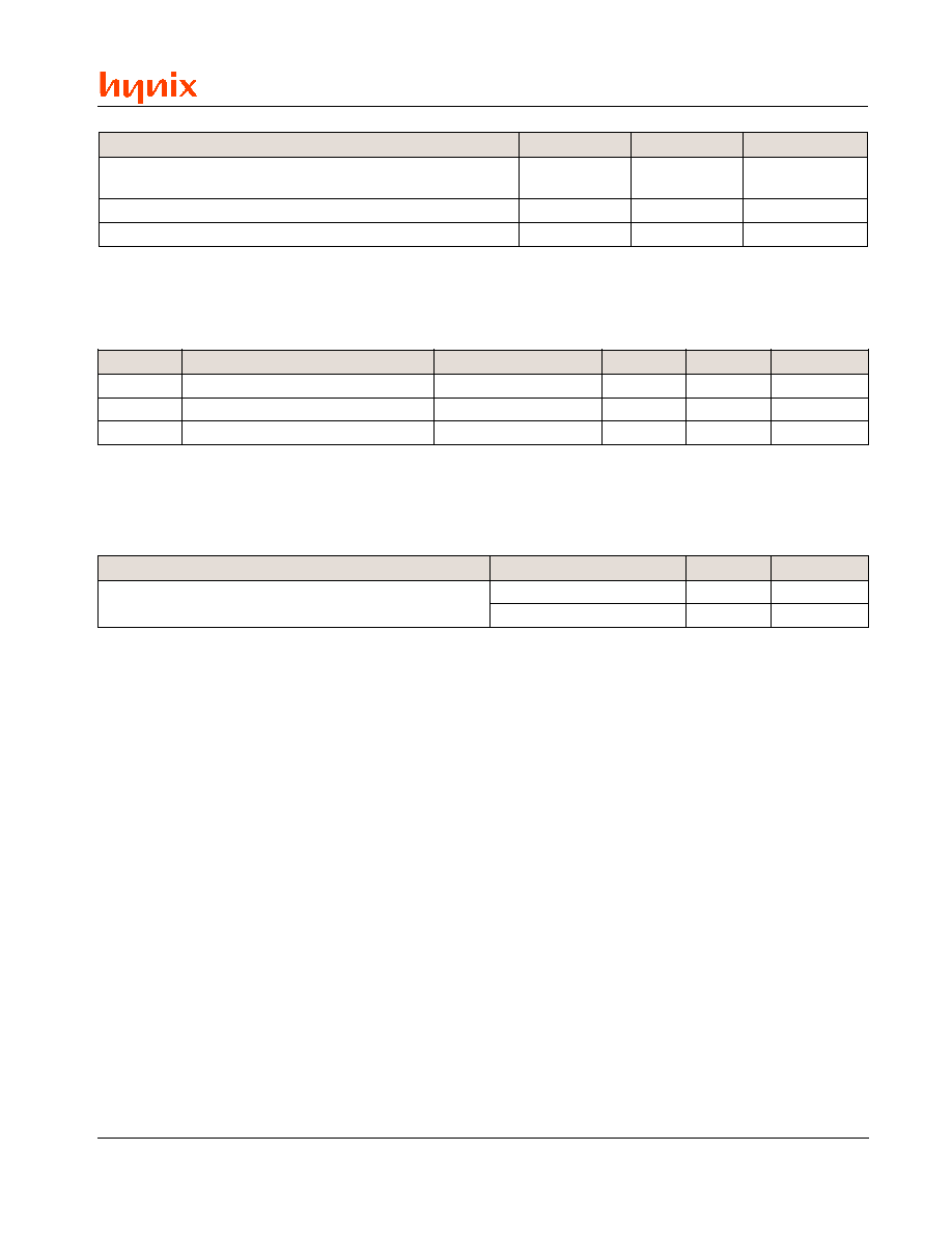
39
Rev. 1.2/May 01
HY29LV160
Latchup Characteristics
Notes:
1. Includes all pins except V
CC
. Test conditions: V
CC
= 3.0V, one pin at a time.
TSOP Pin Capacitance
Notes:
1. Sampled, not 100% tested.
2. Test conditions: T
A
= 25 ∫C, f = 1.0 MHz.
n
o
i
t
p
i
r
c
s
e
D
m
u
m
i
n
i
M
m
u
m
i
x
a
M
t
i
n
U
V
o
t
t
c
e
p
s
e
r
h
t
i
w
e
g
a
t
l
o
v
t
u
p
n
I
S
S
O
/
I
t
p
e
c
x
e
s
n
i
p
ll
a
n
o
)
#
T
E
S
E
R
d
n
a
#
E
O
,
]
9
[
A
g
n
i
d
u
l
c
n
i
(
s
n
i
p
0
.
1
-
5
.
2
1
V
V
o
t
t
c
e
p
s
e
r
h
t
i
w
e
g
a
t
l
o
v
t
u
p
n
I
S
S
s
n
i
p
O
/
I
ll
a
n
o
0
.
1
-
V
C
C
0
.
1
+
V
V
C
C
t
n
e
r
r
u
C
0
0
1
-
0
0
1
A
m
l
o
b
m
y
S
r
e
t
e
m
a
r
a
P
p
u
t
e
S
t
s
e
T
p
y
T
x
a
M
t
i
n
U
C
N
I
e
c
n
a
t
i
c
a
p
a
C
t
u
p
n
I
V
N
I
0
=
6
5
.
7
F
p
C
T
U
O
e
c
n
a
t
i
c
a
p
a
C
t
u
p
t
u
O
V
T
U
O
0
=
5
.
8
2
1
F
p
C
2
N
I
e
c
n
a
t
i
c
a
p
a
C
n
i
P
l
o
r
t
n
o
C
V
N
I
0
=
5
.
7
9
F
p
Data Retention
r
e
t
e
m
a
r
a
P
s
n
o
i
t
i
d
n
o
C
t
s
e
T
m
u
m
i
n
i
M
t
i
n
U
e
m
i
T
n
o
i
t
n
e
t
e
R
a
t
a
D
n
r
e
t
t
a
P
m
u
m
i
n
i
M
C
∫
0
5
1
0
1
s
r
a
e
Y
C
∫
5
2
1
0
2
s
r
a
e
Y
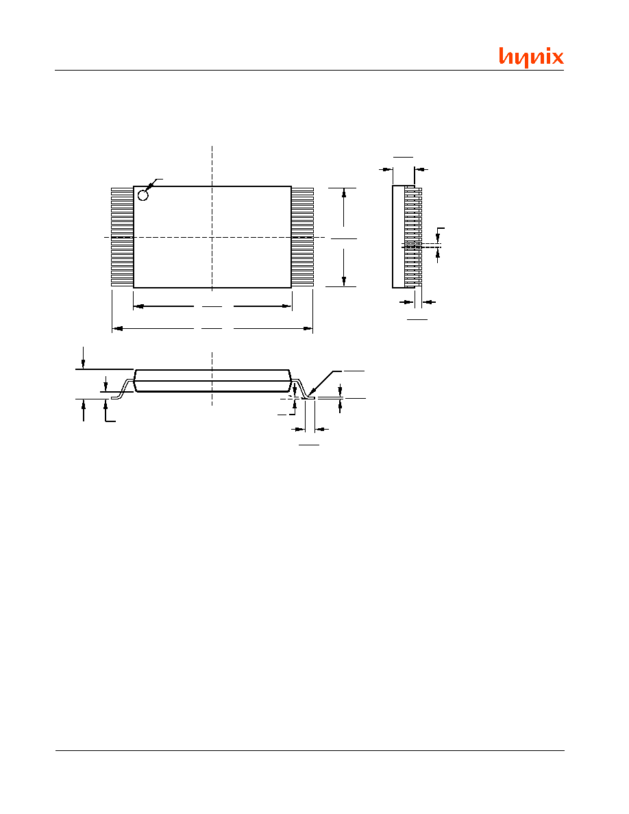
40
Rev. 1.2/May 01
HY29LV160
PACKAGE DRAWINGS
Physical Dimensions
TSOP48 - 48-pin Thin Small Outline Package (measurements in millimeters)
18.30
18.50
Pin 1 ID
11.90
12.10
0.25MM (0.0098") BSC
1.20
MAX
1
24
48
25
19.80
20.20
0.50 BSC
0.95
1.05
0.50
0.70
0
5
o
o
0.10
0.21
0.08
0.20
0.05
0.15
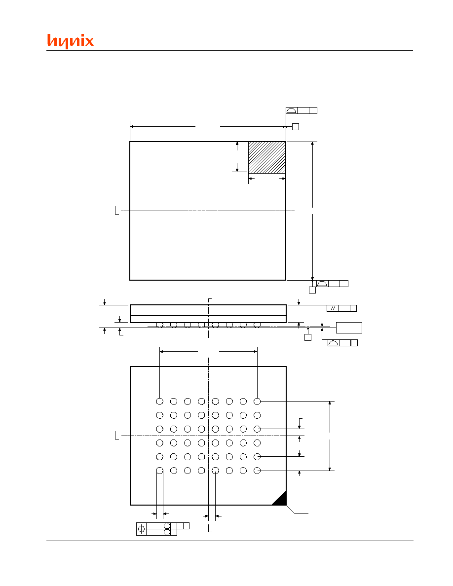
41
Rev. 1.2/May 01
HY29LV160
PACKAGE DRAWINGS
Physical Dimensions
FBGA48 - 48-Ball Fine-Pitch Ball Grid Array, 8 x 9 mm (measurements in millimeters)
Note: Unless otherwise specified, tolerance = ± 0.05
1.10
M A X
0.20
MIN
C
C
0.08
0.76
TYP
C
0.10
Seating
Plane
A1 CORNER
INDEX AREA
9.00 ± 0.10
8.00 ± 0.10
A
B
C
0.10
C
0.10
C
C
2.10 ± 0.10
1.80
± 0.10
Pin A1
Index Mark
4.00 BSC
5.60 BSC
A
B
C
D
E
F
G
H
6
5
4
3
2
1
0.40
B S C
0.80 TYP
0.40
B S C
0.30 ± 0.05
ÿ
ÿ 0.15
M
C A B
ÿ 0.08
M
C
C
C
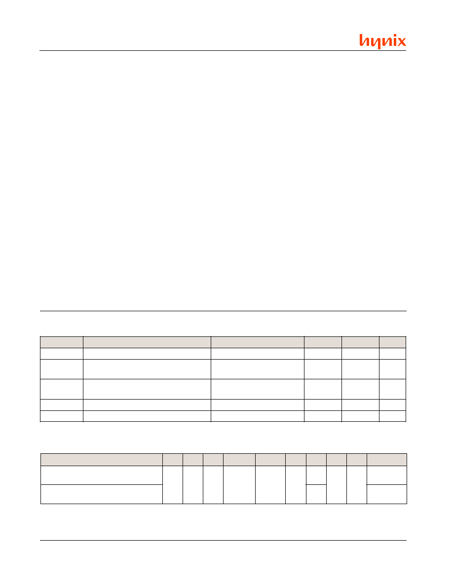
42
Rev. 1.2/May 01
HY29LV160
SECTOR PROTECTION/UNPROTECTION
USING PROGRAMMING EQUIPMENT
In addition to in-situ sector protection/unprotec-
tion, described in the Bus Operations section, the
HY29LV160 is capable of performing the same
functions using programming equipment. This
appendix describes the procedures and provides
specifications for these functions.
Sector Protect
The hardware sector protection feature disables
both program and erase operations in any sector
or combination of sectors.
The method intended for programming equipment
requires a high voltage (V
ID
) on address pin A[9]
and the OE# pin. The flow chart in Figure A1 il-
lustrates the algorithm, and timing specifications
and waveforms are provided at the end of this sec-
tion. When implementing the algorithm, note that
V
CC
must be applied to the device before applying
V
ID
, and V
ID
should be removed before removing
V
CC
from the device.
Programming of the protection circuitry begins on
the falling edge of WE# and is terminated on the
APPENDIX
rising edge of the same pulse. Verification of pro-
tection is done as described in the Electronic ID
Mode section and shown in the flow chart.
The HY29LV160 is shipped with all sectors un-
protected.
Sector Unprotect
The hardware sector unprotection feature re-en-
ables both program and erase operations in pre-
viously protected sectors. Note that to unprotect
any sector, all unprotected sectors must first be
protected prior to the first sector unprotect write
cycle.
The method intended for programming equipment
requires a high voltage (V
ID
) on address pin A[9]
and the OE# pin. The flow chart in Figure A2 illus-
trates the algorithm, and timing specifications and
waveforms are given at the end of this section.
When implementing the algorithm, note that V
CC
must be applied to the device before applying V
ID
,
and V
ID
should be removed before removing V
CC
from the device.
DC CHARACTERISTICS
Sector Protection and Unprotection Using Programming Equipment
r
e
t
e
m
a
r
a
P
n
o
i
t
p
i
r
c
s
e
D
s
n
o
i
t
i
d
n
o
C
t
s
e
T
n
i
M
x
a
M
t
i
n
U
V
C
C
y
l
p
p
u
S
r
e
w
o
P
g
n
i
t
a
r
e
p
O
0
.
3
6
.
3
V
V
D
I
t
c
e
t
o
r
p
n
U
,
t
c
e
t
o
r
P
r
o
t
c
e
S
r
o
f
e
g
a
t
l
o
V
y
f
i
r
e
V
d
n
a
V
C
C
V
0
.
3
=
5
.
1
1
5
.
2
1
V
I
T
I
L
t
n
e
r
r
u
C
d
a
o
L
t
u
p
n
I
e
g
a
t
l
o
V
h
g
i
H
)
#
E
O
,
]
9
[
A
(
V
C
C
V
=
C
C
x
a
M
V
5
.
2
1
=
#
E
O
=
]
9
[
A
5
3
A
µ
V
L
I
e
g
a
t
l
o
V
w
o
L
t
u
p
n
I
5
.
0
-
8
.
0
V
V
H
I
e
g
a
t
l
o
V
h
g
i
H
t
u
p
n
I
0
.
2
V
C
C
5
.
0
+
V
n
o
i
t
a
r
e
p
O
#
E
C
#
E
O
#
E
W
#
T
E
S
E
R
]
2
1
:
9
1
[
A
]
9
[
A
]
6
[
A
]
1
[
A
]
0
[
A
]
0
:
7
[
Q
D
n
o
i
t
a
c
i
f
i
r
e
V
t
c
e
t
o
r
P
r
o
t
c
e
S
L
L
H
H
r
o
t
c
e
S
s
s
e
r
d
d
A
V
D
I
L
H
L
1
0
x
0
n
o
i
t
a
c
i
f
i
r
e
V
t
c
e
t
o
r
p
n
U
r
o
t
c
e
S
H
0
0
x
0
Sector Protection and Unprotection Verification Using Programming Equipment
1
Notes:
1. L = V
IL
, H = V
IH
.
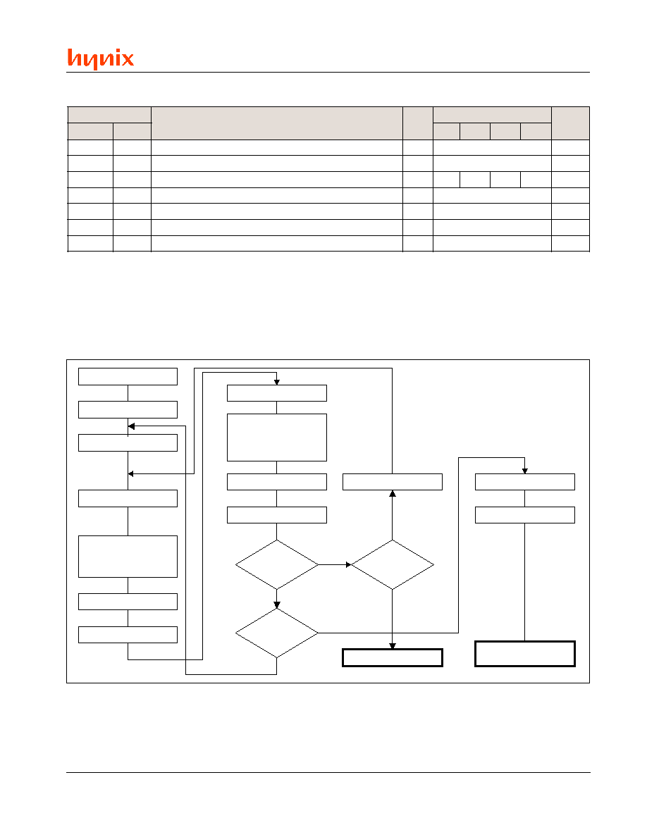
43
Rev. 1.2/May 01
HY29LV160
S T A R T
Set TRYCNT = 1
A9 = OE# = V
ID
Set Address:
A[19:12] = Sector to Protect
CE# = A[6] = A]0] = V
IL
RESET# = A[1] = V
IH
Wait 4 us
WE# = V
IL
Wait 150 us
A[9] = V
ID
A[19:12] = Sector to Protect
OE# = CE# = V
IL
A[6] = A[0] = V
IL
WE# = RESET# = A[1] = V
IH
Read Data
Data = 0x01?
Protect Another
Sector?
YES
TRYCNT = 25?
N O
Increment TRYCNT
N O
YES
DEVICE FAILURE
YES
N O
Remove V
ID
from A[9]
Write Reset Command
SECTOR PROTECT
C O M P L E T E
APPLY V
C C
Wait 4 us
Figure A1. Sector Protection Using Programming Equipment
r
e
t
e
m
a
r
a
P
n
o
i
t
p
i
r
c
s
e
D
n
o
i
t
p
O
d
e
e
p
S
t
i
n
U
C
E
D
E
J
d
t
S
0
7
-
0
8
-
0
9
-
2
1
-
t
R
D
I
V
e
m
i
T
n
o
i
t
i
s
n
a
r
T
e
g
a
t
l
o
V
1
n
i
M
0
0
5
s
n
t
T
S
e
m
i
T
p
u
t
e
S
e
g
a
t
l
o
V
n
i
M
4
s
µ
t
E
O
y
a
l
e
D
t
u
p
t
u
O
o
t
e
l
b
a
n
E
t
u
p
t
u
O
x
a
M
0
3
0
3
5
3
0
5
s
n
t
1
P
P
W
n
o
i
t
a
r
e
p
O
t
c
e
t
o
r
P
r
o
t
c
e
S
r
o
f
h
t
d
i
W
e
s
l
u
P
e
t
i
r
W
n
i
M
0
5
1
s
µ
t
2
P
P
W
n
o
i
t
a
r
e
p
O
t
c
e
t
o
r
p
n
U
r
o
t
c
e
S
r
o
f
h
t
d
i
W
e
s
l
u
P
e
t
i
r
W
n
i
M
5
1
s
m
t
P
S
E
O
e
v
i
t
c
A
#
E
W
o
t
e
m
i
T
p
u
t
e
S
#
E
O
1
n
i
M
4
s
µ
t
P
S
C
e
v
i
t
c
A
#
E
W
o
t
e
m
i
T
p
u
t
e
S
#
E
C
1
n
i
M
4
s
µ
AC CHARACTERISTICS
Sector Protection and Unprotection Using Programming Equipment
Notes:
1. Not 100% tested.
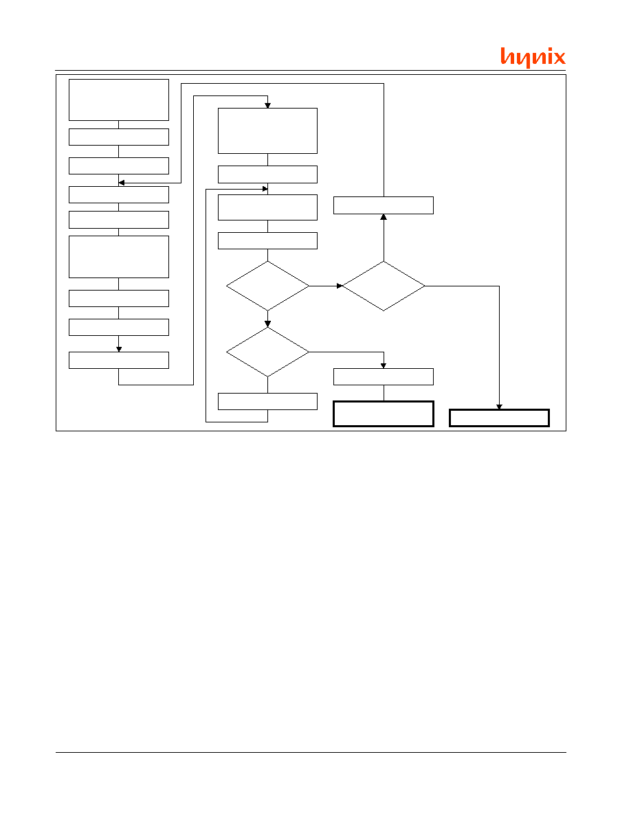
44
Rev. 1.2/May 01
HY29LV160
S T A R T
N O T E : A l l s e c t o r s m u s t b e
previously protected. See
Figure A1.
S e t T R Y C N T = 1
S E T A [ 9 ] = O E # = V
ID
S E T
C E # = A [ 0 ] = V
IL
R E S E T # = A [ 1 ] = A [ 6 ] = V
IH
W a i t 4 u s
W E # = V
IL
W a i t 1 5 m s
S E T
A[9] = V
ID
O E # = C E # = A [ 0 ] = V
IL
W E # = V
IH
R E S E T # = A [ 1 ] = A [ 6 ] = V
IH
R e a d D a t a
D a t a = 0 x 0 0 ?
N S E C = 3 4 ?
Y E S
T R Y C N T = 1 0 0 0 ?
N O
I n c r e m e n t T R Y C N T
N O
Y E S
DEVICE FAILURE
N O
Y E S
R e m o v e V
ID
from A[9]
SECTOR UNPROTECT
C O M P L E T E
A P P L Y V
C C
W a i t 4 u s
S E T S e c t o r A d d r e s s :
A [ 1 9 : 1 2 ] = S e c t o r N S E C
N S E C = N S E C + 1
S E T N S E C = 0
Figure A2. Sector Unprotect Using Programming Equipment
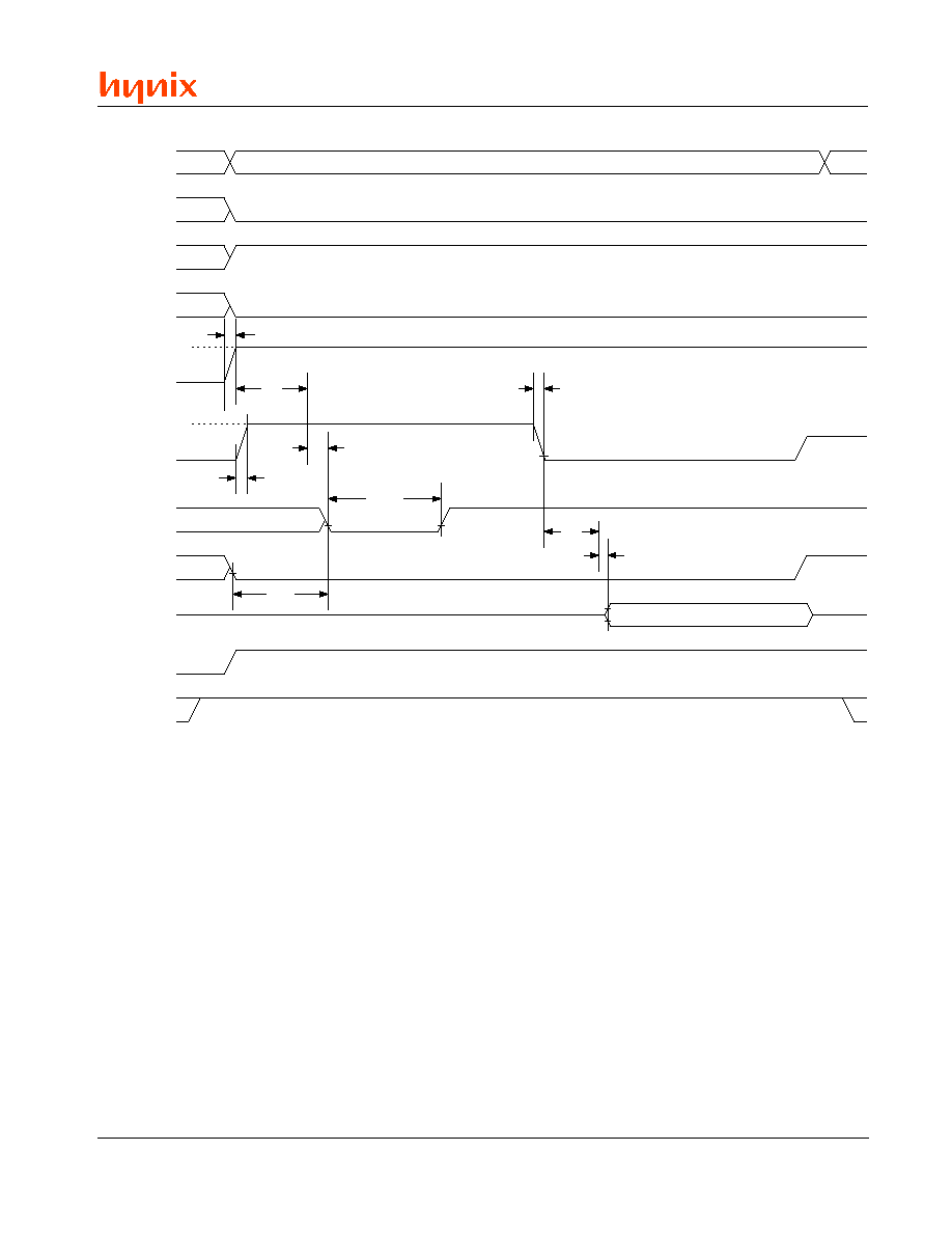
45
Rev. 1.2/May 01
HY29LV160
AC CHARACTERISTICS
Figure A3. Timings for Sector Protection Using Programming Equipment
V
C C
R E S E T #
Data
C E #
W E #
O E #
A[9]
A[6]
A[1]
A[0]
A[19:12]
V
ID
V
ID
S A
X
S A
Y
0x01
t
O E
t
S T
t
V I D R
t
V I D R
t
V I D R
t
O E S P
t
W P P 1
t
C S P
t
S T
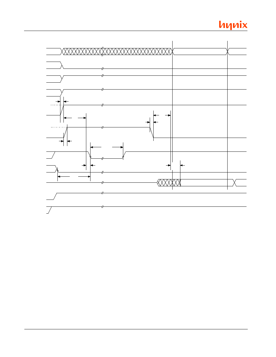
46
Rev. 1.2/May 01
HY29LV160
AC CHARACTERISTICS
Figure A4. Timings for Sector Unprotect Using Programming Equipment
V
C C
R E S E T #
Data
C E #
W E #
O E #
A[9]
A[6]
A[1]
A[0]
A[19:12]
V
I D
V
I D
S A
0
S A
1
0x00
t
V I D R
t
V I D R
t
V I D R
t
O E S P
t
W P P 2
t
C S P
t
S T
t
S T
t
O E
47
Rev. 1.2/May 01
HY29LV160
ORDERING INFORMATION
Hynix products are available in several speeds, packages and operating temperature ranges. The
ordering part number is formed by combining a number of fields, as indicated below. Refer to the `Valid
Combinations' table, which lists the configurations that are planned to be supported in volume. Please
contact your local Hynix representative or distributor to confirm current availability of specific configura-
tions and to determine if additional configurations have been released.
VALID COMBINATIONS
d
e
e
p
S
d
n
a
e
g
a
k
c
a
P
A
G
B
F
P
O
S
T
e
r
u
t
a
r
e
p
m
e
T
s
n
0
7
s
n
0
8
s
n
0
9
s
n
0
2
1
s
n
0
7
s
n
0
8
s
n
0
9
s
n
0
2
1
s
t
l
o
V
6
.
3
-
7
.
2
=
e
g
a
t
l
o
V
g
n
i
t
a
r
e
p
O
l
a
i
c
r
e
m
m
o
C
-
-
0
8
-
F
0
9
-
F
2
1
-
F
-
-
0
8
-
T
0
9
-
T
2
1
-
T
l
a
i
r
t
s
u
d
n
I
-
-
I
0
8
-
F
I
0
9
-
F
I
2
1
-
F
-
-
I
0
8
-
T
I
0
9
-
T
I
2
1
-
T
s
t
l
o
V
6
.
3
-
0
.
3
=
e
g
a
t
l
o
V
g
n
i
t
a
r
e
p
O
l
a
i
c
r
e
m
m
o
C
0
7
-
F
-
-
-
-
-
-
0
7
-
T
-
-
V
0
9
-
T
V
2
1
-
T
l
a
i
r
t
s
u
d
n
I
I
0
7
-
F
-
-
-
-
-
-
I
0
7
-
T
-
-
-
-
-
-
Note:
1. The complete part number is formed by appending the Boot Block Location code and the suffix shown in the table to the
Device Number. For example, the part number for a 90 ns, Industrial temperature range device in the TSOP package
with the top boot block option is HY29LV160TT-90I.
0
6
1
V
L
9
2
Y
H
X
X
-
X
X
X
S
N
O
I
T
C
U
R
T
S
N
I
L
A
I
C
E
P
S
E
G
N
A
R
E
R
U
T
A
R
E
P
M
E
T
=
k
n
a
l
B
=
I
)
C
∞
0
7
+
o
t
0
(
l
a
i
c
r
e
m
m
o
C
)
C
∞
5
8
+
o
t
0
4
-
(
l
a
i
r
t
s
u
d
n
I
N
O
I
T
P
O
D
E
E
P
S
=
0
7
=
0
8
=
0
9
=
2
1
s
n
0
7
s
n
0
8
s
n
0
9
s
n
0
2
1
E
P
Y
T
E
G
A
K
C
A
P
=
T
=
F
)
P
O
S
T
(
e
g
a
k
c
a
P
e
n
il
t
u
O
ll
a
m
S
n
i
h
T
n
i
P
-
8
4
m
m
9
x
8
,
)
A
G
B
F
(
y
a
r
r
A
d
i
r
G
ll
a
B
h
c
t
i
P
-
e
n
i
F
ll
a
B
-
8
4
N
O
I
T
A
C
O
L
K
C
O
L
B
T
O
O
B
=
T
=
B
n
o
i
t
p
O
k
c
o
l
B
t
o
o
B
p
o
T
n
o
i
t
p
O
k
c
o
l
B
t
o
o
B
m
o
t
t
o
B
R
E
B
M
U
N
E
C
I
V
E
D
=
0
6
1
V
L
9
2
Y
H
r
o
t
c
e
S
y
l
n
O
-
t
l
o
V
3
S
O
M
C
)
6
1
x
M
1
/
8
x
M
2
(
t
i
b
a
g
e
M
6
1
y
r
o
m
e
M
h
s
a
l
F
e
s
a
r
E

48
Rev. 1.2/May 01
HY29LV160
Important Notice
© 2001 by Hynix Semiconductor America. All rights reserved.
No part of this document may be copied or reproduced in any
form or by any means without the prior written consent of Hynix
Semiconductor Inc. or Hynix Semiconductor America (collec-
tively "Hynix").
The information in this document is subject to change without
notice. Hynix shall not be responsible for any errors that may
appear in this document and makes no commitment to update
or keep current the information contained in this document.
Hynix advises its customers to obtain the latest version of the
device specification to verify, before placing orders, that the
information being relied upon by the customer is current.
Devices sold by Hynix are covered by warranty and patent
indemnification provisions appearing in Hynix Terms and Con-
ditions of Sale only. Hynix makes no warranty, express, statu-
tory, implied or by description, regarding the information set
forth herein or regarding the freedom of the described devices
from intellectual property infringement. Hynix makes no war-
ranty of merchantability or fitness for any purpose.
Hynix's products are not authorized for use as critical compo-
nents in life support devices or systems unless a specific writ-
ten agreement pertaining to such intended use is executed
between the customer and Hynix prior to use. Life support
devices or systems are those which are intended for surgical
implantation into the body, or which sustain life whose failure
to perform, when properly used in accordance with instruc-
tions for use provided in the labeling, can be reasonably ex-
pected to result in significant injury to the user.
d
r
o
c
e
R
n
o
i
s
i
v
e
R
.
v
e
R
e
t
a
D
s
l
i
a
t
e
D
2
.
1
1
0
/
5
.
t
a
m
r
o
f
x
i
n
y
H
o
t
e
g
n
a
h
C
.
n
o
i
t
c
e
s
s
n
o
i
t
a
r
u
g
i
f
n
o
C
n
i
P
n
i
w
e
i
v
A
G
B
F
f
o
n
o
i
t
p
i
r
c
s
e
d
d
e
t
c
e
r
r
o
C
.
s
n
o
i
t
p
o
e
c
i
v
e
d
V
2
1
-
d
n
a
V
0
9
-
d
e
d
d
A
.
n
o
i
t
p
o
e
r
u
t
a
r
e
p
m
e
t
d
e
d
n
e
t
x
E
d
e
v
o
m
e
R
Memory Sales and Marketing Division
Flash Memory Business Unit
Hynix Semiconductor Inc.
Hynix Semiconductor America Inc.
10 Fl., Hynix Youngdong Building
3101 North First Street
89, Daechi-dong
San Jose, CA 95134
Kangnam-gu
USA
Seoul, Korea
Telephone: (408) 232-8800
Telephone: +82-2-580-5000
Fax: (408) 232-8805
Fax: +82-2-3459-3990
http://www.us.hynix.com
http://www.hynix.com