H Y 5 7 V 6 4 1 6 2 0 H G
4 Banks x 1M x 16Bit Synchronous DRAM
This document is a general product description and is subject to change without notice. Hyundai Electronics does not assume any responsibility for use of
circuits described. No patent licenses are implied.
Rev. 0.5/Jun.01
D E S C R IP T IO N
The Hynix HY57V641620HG is a 67,108,864-bit CMOS Synchronous DRAM, ideally suited for the main memory applications which
require large memory density and high bandwidth. HY57V641620HG is organized as 4banks of 1,048,576x16.
HY57V641620HG is offering fully synchronous operation referenced to a positive edge of the clock. All inputs and outputs are synchro-
nized with the rising edge of the clock input. The data paths are internally pipelined to achieve very high bandwidth. All input and output
voltage levels are compatible with LVTTL.
Programmable options include the length of pipeline (Read latency of 2 or 3), the number of consecutive read or write cycles initiated
by a single control command (Burst length of 1,2,4,8 or Full page), and the burst count sequence(sequential or interleave). A burst of
read or write cycles in progress can be terminated by a burst terminate command or can be interrupted and replaced by a new burst
read or write command on any cycle. (This pipelined design is not restricted by a `2N` rule.)
F E A T U R E S
∑
Single 3.3
±
0 . 3 V p o w e r s u p p l y
N o t e )
∑
A l l d e v i c e p i n s a r e c o m p a t i b l e w i t h L V T T L i n t e r f a c e
∑
J E D E C s t a n d a r d 4 0 0 m i l 5 4 p i n T S O P - I I w i t h 0 . 8 m m
o f p i n p i t c h
∑
A l l i n p u t s a n d o u t p u t s r e f e r e n c e d t o p o s i t i v e e d g e o f
s y s t e m c l o c k
∑
D a t a m a s k f u n c t i o n b y U D Q M o r L D Q M
∑
I n t e r n a l f o u r b a n k s o p e r a t i o n
∑
A u t o r e f r e s h a n d s e l f r e f r e s h
∑
4 0 9 6 r e f r e s h c y c l e s / 6 4 m s
∑
P r o g r a m m a b l e B u r s t L e n g t h a n d B u r s t T y p e
- 1 , 2 , 4 , 8 o r F u l l p a g e f o r S e q u e n t i a l B u r s t
- 1 , 2 , 4 o r 8 f o r I n t e r l e a v e B u r s t
∑
P r o g r a m m a b l e C A S L a t e n c y ; 2 , 3 C l o c k s
O R D E R IN G IN F O R M A T IO N
N o t e : V D D ( M in ) o f H Y 5 7 V 6 4 1 6 2 0 H G ( L ) T - 5 /5 5 / 6 i s 3 . 1 3 5 V
P a r t N o .
C l o c k F r e q u e n c y
P o w e r
Organization
Interface
P a c k a g e
H Y 5 7 V 6 4 1 6 2 0 H G T - 5 / 5 5 / 6 / 7
2 0 0 / 1 8 3 / 1 6 6 / 1 4 3 M H z
N o r m a l
4 B a n k s x 1 M b i t s
x 1 6
L V T T L
4 0 0 m i l 5 4 p i n T S O P I I
H Y 5 7 V 6 4 1 6 2 0 H G T - K
1 3 3 M H z
H Y 5 7 V 6 4 1 6 2 0 H G T - H
1 3 3 M H z
H Y 5 7 V 6 4 1 6 2 0 H G T - 8
1 2 5 M H z
H Y 5 7 V 6 4 1 6 2 0 H G T - P
1 0 0 M H z
H Y 5 7 V 6 4 1 6 2 0 H G T - S
1 0 0 M H z
H Y 5 7 V 6 4 1 6 2 0 H G L T - 5 / 5 5 / 6 / 7
2 0 0 / 1 8 3 / 1 6 6 / 1 4 3 M H z
L o w p o w e r
H Y 5 7 V 6 4 1 6 2 0 H G L T - K
1 3 3 M H z
H Y 5 7 V 6 4 1 6 2 0 H G L T - H
1 3 3 M H z
H Y 5 7 V 6 4 1 6 2 0 H G L T - 8
1 2 5 M H z
H Y 5 7 V 6 4 1 6 2 0 H G L T - P
1 0 0 M H z
H Y 5 7 V 6 4 1 6 2 0 H G L T - S
1 0 0 M H z
H Y 5 7 V 6 4 1 6 2 0 H G
R e v . 0 . 5 / J u n . 0 1
2
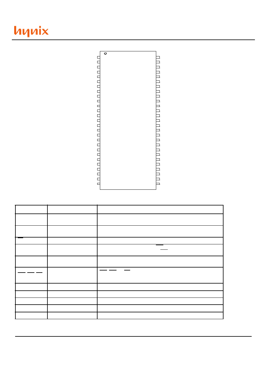
P IN C O N F IG U R A T IO N
P IN D E S C R IP T IO N
PIN
P I N N A M E
D E S C R I P T I O N
C L K
C l o c k
T h e s y s t e m c l o c k i n p u t . A l l o t h e r i n p u t s a r e r e g i s t e r e d t o t h e S D R A M o n t h e
r i s i n g e d g e o f C L K
C K E
C l o c k E n a b l e
C o n t r o l s i n t e r n a l c l o c k s i g n a l a n d w h e n d e a c t i v a t e d , t h e S D R A M w i l l b e o n e
o f t h e s t a t e s a m o n g p o w e r d o w n , s u s p e n d o r s e l f r e f r e s h
C S
C h i p S e l e c t
E n a b l e s o r d i s a b l e s a l l i n p u t s e x c e p t C L K , C K E a n d D Q M
B A 0 , B A 1
B a n k A d d r e s s
S e l e c t s b a n k t o b e a c t i v a t e d d u r i n g R A S activity
S e l e c t s b a n k t o b e r e a d / w r i t t e n d u r i n g C A S activity
A 0 ~ A 1 1
A d d r e s s
R o w A d d r e s s : R A 0 ~ R A 1 1 , C o l u m n A d d r e s s : C A 0 ~ C A 7
A u t o - p r e c h a r g e f l a g : A 1 0
R A S , C A S, W E
R o w A d d r e s s S t r o b e ,
C o l u m n A d d r e s s S t r o b e ,
W r i t e E n a b l e
R A S , C A S a n d W E d e f i n e t h e o p e r a t i o n
R e f e r f u n c t i o n t r u t h t a b l e f o r d e t a i l s
L D Q M , U D Q M
D a t a I n p u t / O u t p u t M a s k
C o n t r o l s o u t p u t b u f f e r s i n r e a d m o d e a n d m a s k s i n p u t d a t a i n w r i t e m o d e
D Q 0 ~ D Q 1 5
D a t a I n p u t / O u t p u t
M u l t i p l e x e d d a t a i n p u t / o u t p u t p i n
V
D D
/V
S S
P o w e r S u p p l y / G r o u n d
P o w e r s u p p l y f o r i n t e r n a l c i r c u i t s a n d i n p u t b u f f e r s
V
D D Q
/V
S S Q
D a t a O u t p u t P o w e r / G r o u n d
P o w e r s u p p l y f o r o u t p u t b u f f e r s
N C
N o C o n n e c t i o n
N o c o n n e c t i o n
V SS
D Q 1 5
V SSQ
D Q 1 4
D Q 1 3
V DDQ
D Q 1 2
D Q 1 1
V SSQ
D Q 1 0
DQ9
V DDQ
DQ8
V SS
N C
UDQM
CLK
CKE
N C
A11
A 9
A 8
A 7
A 6
A 5
A 4
V SS
1
2
3
4
5
6
7
8
9
1 0
1 1
1 2
1 3
1 4
1 5
1 6
1 7
1 8
1 9
2 0
2 1
2 2
2 3
2 4
2 5
2 6
2 7
5 4
5 3
5 2
5 1
5 0
4 9
4 8
4 7
4 6
4 5
4 4
4 3
4 2
4 1
4 0
3 9
3 8
3 7
3 6
3 5
3 4
3 3
3 2
3 1
3 0
2 9
2 8
VDD
DQ0
VDDQ
DQ1
DQ2
VSSQ
DQ3
DQ4
VDDQ
DQ5
DQ6
VSSQ
DQ7
VDD
L D Q M
/ W E
/CAS
/RAS
/ C S
BA0
BA1
A10/AP
A 0
A 1
A 2
A 3
VDD
54pin TSOP II
400mil x 875mil
0.8mm pin pitch
H Y 5 7 V 6 4 1 6 2 0 H G
R e v . 0 . 5 / J u n . 0 1
3
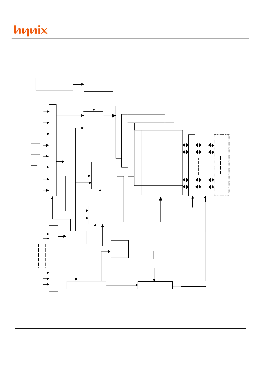
F U N C T IO N A L B L O C K D IA G R A M
1 M b i t x 4 b a n k s x 1 6 I / O S y n c h r o n o u s D R A M
X decoders
State Machine
A 0
A 1
A 1 1
B A 0
B A 1
Address buffers
A d d r e s s
R e g i s t e r s
M o d e R e g i s t e r s
R o w
P r e
D e c o d e r s
C o l u m n
P r e
D e c o d e r s
C o l u m n A d d
C o u n t e r
R o w a c t i v e
C o l u m n
A c t i v e
B u r s t
C o u n t e r
D a t a O u t C o n t r o l
C A S L a t e n c y
I n t e r n a l R o w
c o u n t e r
D Q 0
D Q 1
D Q 1 4
D Q 1 5
r e f r e s h
S e l f r e f r e s h l o g i c
& t i m e r
P i p e L i n e C o n t r o l
I/O Buffer & Logic
B a n k S e l e c t
Sense AMP & I/O Gate
C L K
C K E
C S
R A S
C A S
W E
U D Q M
L D Q M
1 M x 1 6 B a n k 3
X decoders
X decoders
M e m o r y
Cell
A r r a y
Y d e c o d e r s
X decoders
1 M x 1 6 B a n k 0
1 M x 1 6 B a n k 1
1 M x 1 6 B a n k 2
H Y 5 7 V 6 4 1 6 2 0 H G
R e v . 0 . 5 / J u n . 0 1
4
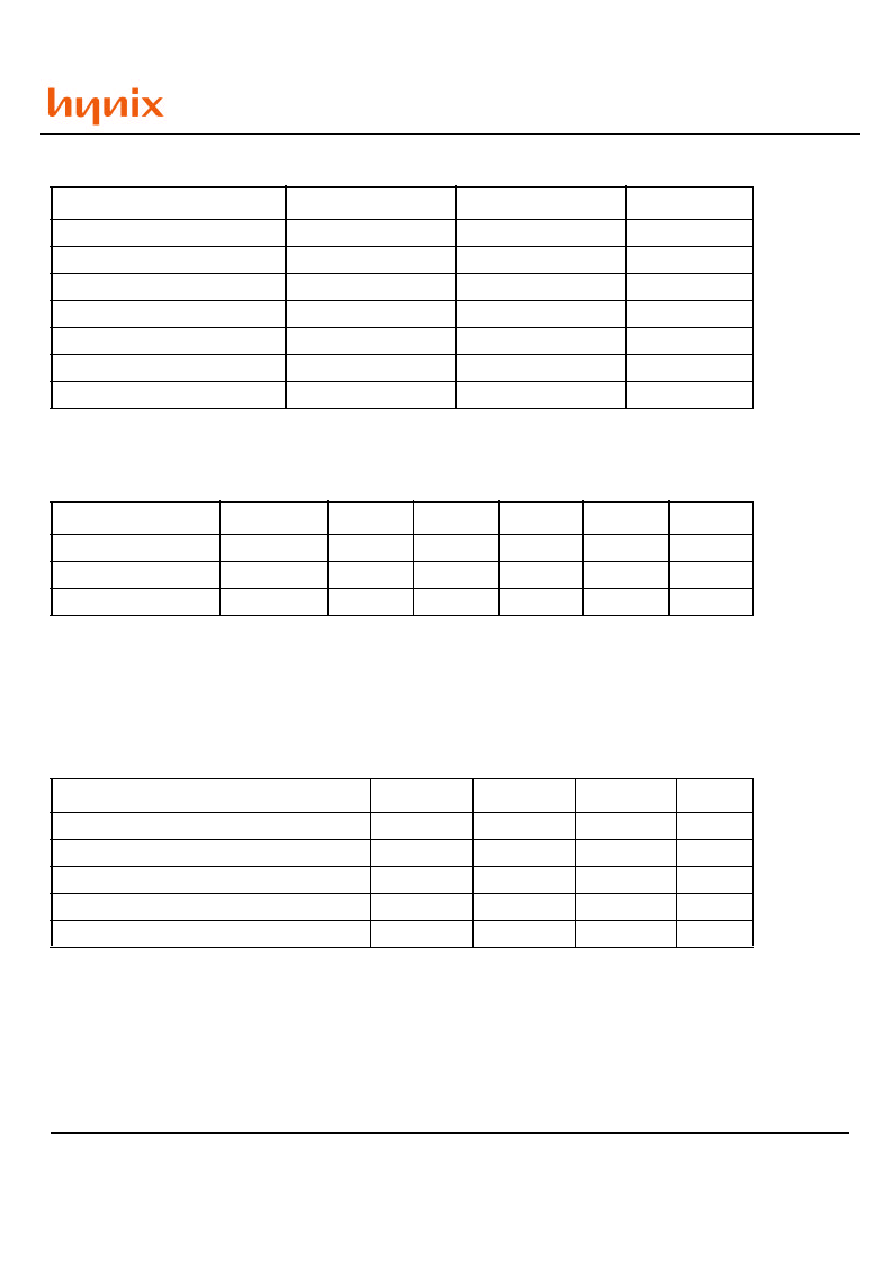
A B S O L U T E M A X IM U M R A T IN G S
N o te :
O p e r a t i o n a t a b o v e a b s o l u t e m a x i m u m r a t i n g c a n a d v e r s e l y a f f e c t d e v i c e r e l i a b i l i t y
D C O P E R A T IN G C O N D IT IO N
( T A = 0 t o 7 0
∞
C
)
N o te :
1 . A l l v o l t a g e s a r e r e f e r e n c e d t o V
S S
= 0 V
2 . V D D ( m i n ) o f H Y 5 7 V 6 4 1 6 2 0 H G ( L ) T - 5 / 5 5 / 6 i s 3 . 1 3 5 V
3.V
I H
( m a x ) i s a c c e p t a b l e 5 . 6 V A C p u l s e w i d t h w i t h
3 n s o f d u r a t i o n
4.V
I L
( m i n ) i s a c c e p t a b l e - 2 . 0 V A C p u l s e w i d t h w i t h
3 n s o f d u r a t i o n
A C O P E R A T IN G C O N D IT IO N
( T A = 0 t o 7 0
∞
C
, V
D D
= 3 . 3
±
0 . 3 V
Note2
, V
S S
= 0 V )
N o te :
1 . O u t p u t l o a d t o m e a s u r e a c c e s s t i m e i s e q u i v a l e n t t o t w o T T L g a t e s a n d o n e c a p a c i t o r ( 5 0 p F )
F o r d e t a i l s , r e f e r t o A C / D C o u t p u t c i r c u i t
2 . V D D ( m i n ) o f H Y 5 7 V 6 4 1 6 2 0 H G ( L ) T - 5 / 5 5 / 6 i s 3 . 1 3 5 V
P a r a m e t e r
S y m b o l
R a t i n g
U n i t
A m b i e n t T e m p e r a t u r e
T
A
0 ~ 7 0
∞
C
S t o r a g e T e m p e r a t u r e
T
S T G
- 5 5 ~ 1 2 5
∞
C
V o l t a g e o n A n y P i n r e l a t i v e t o V
S S
V
I N
, V
O U T
- 1 . 0 ~ 4 . 6
V
V o l t a g e o n V
D D
relative to V
S S
V
D D ,
V
D D Q
- 1 . 0 ~ 4 . 6
V
S h o r t C i r c u i t O u t p u t C u r r e n t
I
O S
5 0
m A
P o w e r D i s s i p a t i o n
P
D
1
W
S o l d e r i n g T e m p e r a t u r e
T i m e
T
S O L D E R
2 6 0
1 0
∞
C
S e c
P a r a m e t e r
S y m b o l
M in
T y p .
M a x
U n it
N o te
P o w e r S u p p l y V o l t a g e
V
D D
, V
D D Q
3.0
3.3
3.6
V
1,2
I n p u t H i g h V o l t a g e
V
I H
2.0
3.0
V
D D Q
+ 2 . 0
V
1,3
I n p u t L o w V o l t a g e
V
I L
V
S S Q
- 2 . 0
0
0.8
V
1,4
P a r a m e t e r
S y m b o l
V a l u e
U n it
N o t e
A C I n p u t H i g h / L o w L e v e l V o l t a g e
V
I H
/ V
IL
2.4/0.4
V
I n p u t T i m i n g M e a s u r e m e n t R e f e r e n c e L e v e l V o l t a g e
Vtrip
1.4
V
I n p u t R i s e / F a l l T i m e
tR / tF
1
n s
O u t p u t T i m i n g M e a s u r e m e n t R e f e r e n c e L e v e l
V o u t r e f
1.4
V
O u t p u t L o a d C a p a c i t a n c e f o r A c c e s s T i m e M e a s u r e m e n t
C L
5 0
p F
1
H Y 5 7 V 6 4 1 6 2 0 H G
R e v . 0 . 5 / J u n . 0 1
5
C A P A C IT A N C E
( T A = 2 5
∞
C
, f = 1 M H z )
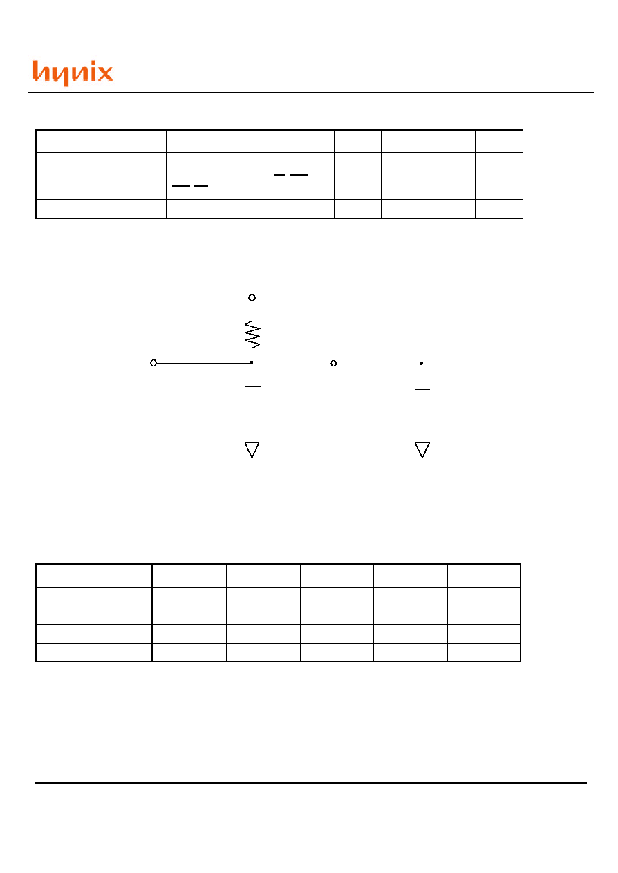
O U T P U T L O A D C IR C U IT
D C C H A R A C T E R IS T IC S I
( T A = 0 t o 7 0
∞
C
, V
D D
= 3 . 3
±
0 . 3 V
Note3
)
N o te :
1.V
I N
= 0 t o 3 . 6 V , A l l o t h e r p i n s a r e n o t t e s t e d u n d e r V
IN
= 0 V
2 . D
O U T
i s d i s a b l e d , V
O U T
= 0 t o 3 . 6
P a r a m e t e r
P in
S y m b o l
M in
M a x
U n i t
I n p u t c a p a c i t a n c e
C L K
C
I1
2
4
p F
A 0 ~ A 1 1 , B A 0 , B A 1 , C K E , C S , R A S ,
C A S , W E , U D Q M , L D Q M
CI
2
2.5
5
p F
D a t a i n p u t / o u t p u t c a p a c i t a n c e
D Q 0 ~ D Q 1 5
C
I/O
2
6.5
p F
P a r a m e t e r
S y m b o l
M i n .
M a x
U n i t
N o t e
I n p u t L e a k a g e C u r r e n t
I
L I
-1
1
u A
1
O u t p u t L e a k a g e C u r r e n t
I
L O
-1
1
u A
2
O u t p u t H i g h V o l t a g e
V
O H
2.4
-
V
I
O H
= - 4 m A
O u t p u t L o w V o l t a g e
V
O L
-
0.4
V
I
O L
= + 4 m A
Vtt=1.4V
RT=250
50pF
Output
50 pF
Output
D C O u t p u t L o a d C i r c u i t
A C O u t p u t L o a d C i r c u i t