This document is a general product description and is subject to change without notice. Hynix does not assume any responsibility for
use of circuits described. No patent licenses are implied.
Rev. 0.3 / Sep. 2004
1
HY57V643220D(L/S)T(P) Series
4Banks x 512K x 32bits Synchronous DRAM
Document Title
4Bank x 512K x 32bits Synchronous DRAM
Revision History
Revision
No.
History
Draft Date
Remark
0.1
Initial Draft
May. 2004
Preliminary
0.2
Removed Preliminary
July 2004
0.3
1. Updated Output Load Capacitance for Access Time Measurement CL = 30pF
in AC OPERATING TEST CONDITION
2. Updated the tolerance zone of the leads and the description of the package
type in PACKAGE DIMENSION
Sep. 2004
This document is a general product description and is subject to change without notice. Hynix does not assume any responsibility for
use of circuits described. No patent licenses are implied.
Rev. 0.3 / Sep. 2004
2
HY57V643220D(L/S)T(P) Series
4Banks x 512K x 32bits Synchronous DRAM
DESCRIPTION
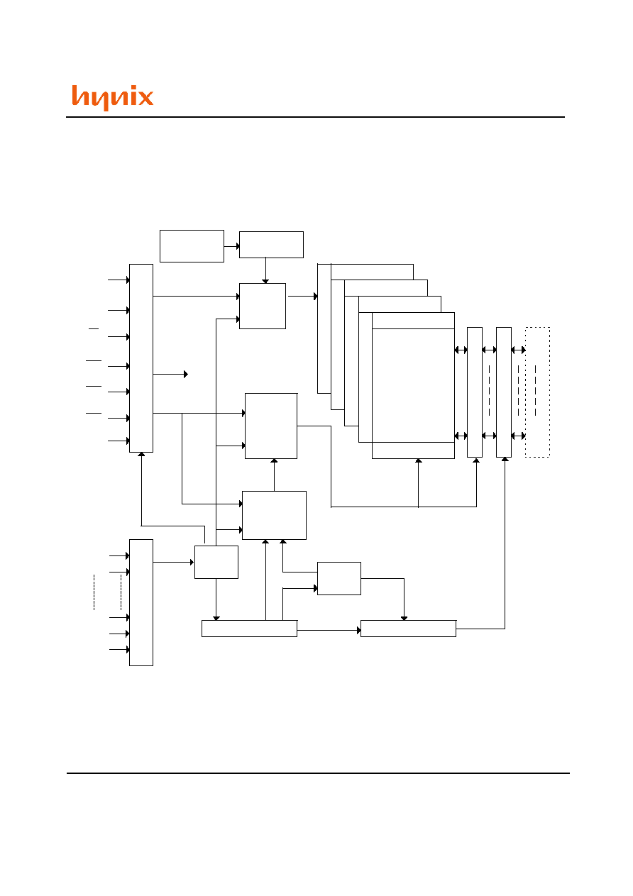
The Hynix HY57V643220D(L/S)T(P) series is a 67,108,864bit CMOS Synchronous DRAM, ideally suited for the memory
applications which require wide data I/O and high bandwidth. HY57V643220D(L/S)T(P) is organized as 4banks of
524,228x32.
HY57V643220D(L/S)T(P) is offering fully synchronous operation referenced to a positive edge of the clock. All inputs
and outputs are synchronized with the rising edge of the clock input. The data paths are internally pipelined to achieve
very high bandwidth. All input and output voltage levels are compatible with LVTTL.
Programmable options include the length of pipeline (Read latency of 2 or 3), the number of consecutive read or write
cycles initiated by a single control command (Burst length of 1,2,4,8 or full page), and the burst count sequence(se-
quential or interleave). A burst of read or write cycles in progress can be terminated by a burst terminate command or
can be interrupted and replaced by a new burst read or write command on any cycle. (This pipelined design is not re-
stricted by a '2N' rule)
FEATURES
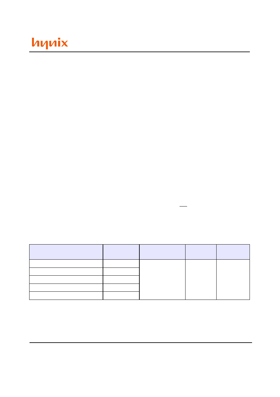
ORDERING INFORMATION
Note
1. HY57V643220DT(P) Series : Normal Power
2. HY57V643220DLT(P) Series : Low Power
3. HY57V643220DST(P) Series : Super Low Power
4. HY57V643220D(L/S)T Series : Leaded
5. HY57V643220D(L/S)TP Series : Lead Free
Part No.
Clock
Frequency
Organization
Interface
Package
HY57V643220D(L/S)T(P)-45
222MHz
4Banks x 512Kbits
x32
LVTTL
86pin TSOP-II
(Lead Free)
HY57V643220D(L/S)T(P)-5
200MHz
HY57V643220D(L/S)T(P)-55
183MHz
HY57V643220D(L/S)T(P)-6
166MHz
HY57V643220D(L/S)T(P)-7
143MHz
�
Voltage : VDD, VDDQ 3.3V supply voltage
�
All device pins are compatible with LVTTL interface
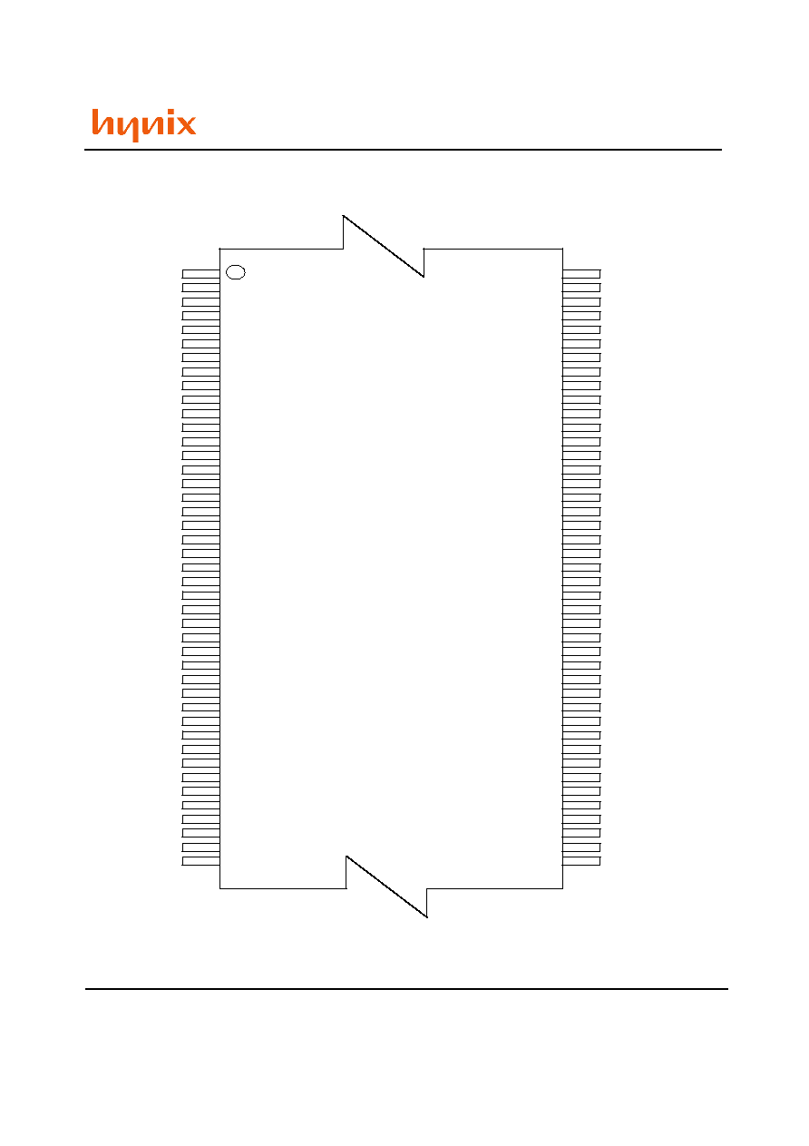
� JEDEC standard 400mil 86pin TSOP-II with 0.5mm of
pin pitch
�
All inputs and outputs referenced to positive edge of
system clock
�
Data mask function by DQM 0, 1, 2 and DQM 3
�
Internal four banks operation
�
Auto refresh and self refresh
�
4096 Refresh cycles / 64ms
�
Programmable Burst Length and Burst Type
- 1, 2, 4, 8 or full page for Sequential Burst
- 1, 2, 4 or 8 for Interleave Burst
�
Programmable CAS Latency ; 2, 3 Clocks
�
Burst Read Single Write operation
Rev. 0.3 / Sep. 2004
4
HY57V643220D(L/S)T(P) Series
4Banks x 512K x 32bits Synchronous DRAM
Pin FUNCTION DESCRIPTIONS
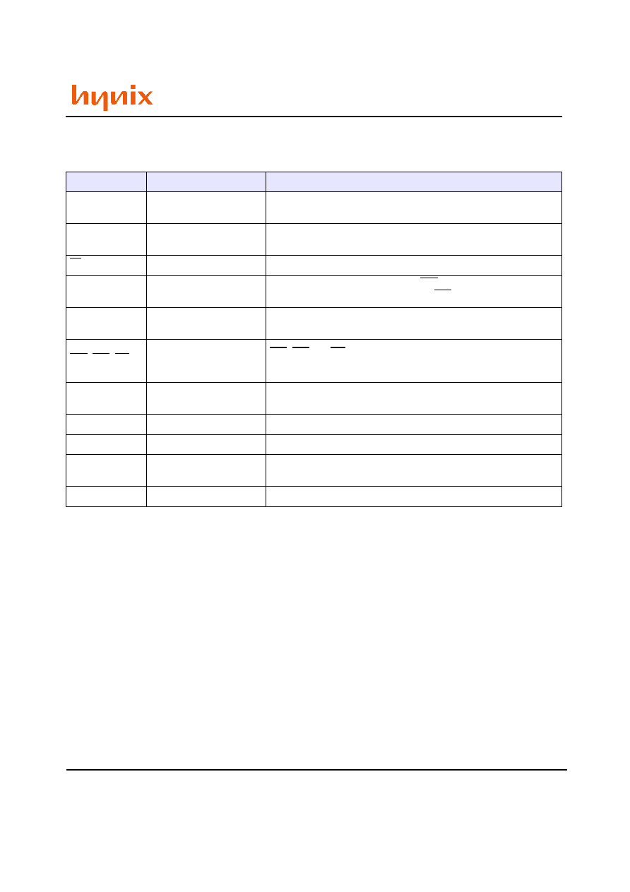
Pin
Pin Name
DESCRIPTION
CLK
Clock
The system clock input. All other inputs are registered to the
SDRAM on the rising edge of CLK.
CKE
Clock Enable
Controls internal clock signal and when deactivated, the SDRAM will
be one of the states among power down, suspend or self refresh
CS
Chip Select
Enables or disables all inputs except CLK, CKE and DQM
BA0, BA1
Bank Address
Selects bank to be activated during RAS activity
Selects bank to be read/written during CAS activity
A0 ~ A10
Address
Row Address : RA0 ~ RA10, Column Address : CA0 ~ CA7
Auto-precharge flag : A10
RAS, CAS, WE
Row Address Strobe,
Column Address Strobe,
Write Enable
RAS, CAS and WE define the operation
Refer function truth table for details
DQM0~3
Data Input/Output Mask
Controls output buffers in read mode and masks input data in write
mode
DQ0 ~ DQ31
Data Input/Output
Multiplexed data input / output pin
VDD/VSS
Power Supply/Ground
Power supply for internal circuits and input buffers
VDDQ/VSSQ
Data Output Power/
Ground
Power supply for output buffers
NC
No Connection
No connection