HY5DU281622DT-6 (Rev 0.2).fm

HY5DU281622DT-6
128M(8Mx16) DDR SDRAM
HY5DU281622DT
This document is a general product description and is subject to change without notice. Hynix Electronics does not assume any
responsibility for use of circuits described. No patent licenses are implied.
Rev. 0.2/ Nov. 02

Rev. 0.2 / Nov. 02
2
HY5DU281622DT-6
Revision History
2. Revision 0.2 (Nov. 02)
1) Defined DC spec.
1. Revision 0.1 (Sep. 02)
1) Defined Preliminary Specification
DESCRIPTION
The Hynix HY5DU281622 is a 134,217,728-bit CMOS Double Data Rate(DDR) Synchronous DRAM, ideally suited for the
point-to-point applications which requires high bandwidth.
The Hynix 8Mx16 DDR SDRAMs offer fully synchronous operations referenced to both rising and falling edges of the
clock. While all addresses and control inputs are latched on the rising edges of the CK (falling edges of the /CK), Data,
Data strobes and Write data masks inputs are sampled on both rising and falling edges of it. The data paths are inter-
nally pipelined and 2-bit prefetched to achieve very high bandwidth. All input and output voltage levels are compatible
with SSTL_2.
FEATURES
�
V
DD
, V
DDQ
= 2.5V +/- 5%
�
All inputs and outputs are compatible with SSTL_2
interface
�
JEDEC standard 400mil 66pin TSOP-II with 0.65mm
pin pitch
�
Fully differential clock inputs (CK, /CK) operation
�
Double data rate interface
�
Source synchronous - data transaction aligned to
bidirectional data strobe (DQS)
�
x16 device has 2 bytewide data strobes (LDQS,
UDQS) per each x8 I/O
�
Data outputs on DQS edges when read (edged DQ)
Data inputs on DQS centers when write (centered
DQ)
�
Data(DQ) and Write masks(DM) latched on the both
rising and falling edges of the data strobe
�
All addresses and control inputs except Data, Data
strobes and Data masks latched on the rising edges
of the clock
�
Write mask byte controls by LDM and UDM
�
Programmable /CAS Latency 3 supported
�
Programmable Burst Length 2 / 4 / 8 with both
sequential and interleave mode
�
Internal 4 bank operations with single pulsed /RAS
�
Auto refresh and self refresh supported
�
4096 refresh cycles / 64ms
�
Full and Half strength driver option controlled by
EMRS
ORDERING INFORMATION
Part No.
Power Supply
Clock
Frequency
Max Data Rate
interface
Package
HY5DU281622DT-6
V
DD/
V
DDQ
=2.5V
166MHz
333Mbps/pin
SSTL_2
400mil 66pin
TSOP-II
HY5DU281622DT-6
Rev. 0.2 / Nov. 02 3
PRELIMINARY
Rev. 0.2 / Nov. 02
4
HY5DU281622DT-6
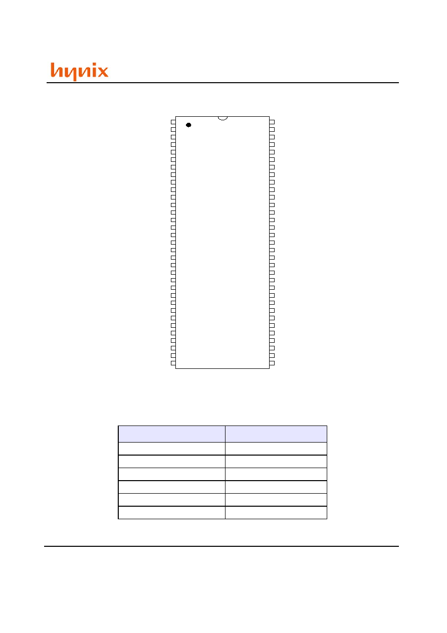
PIN CONFIGURATION
ROW and COLUMN ADDRESS TABLE
Items
8Mx16
Organization
2M x 16 x 4banks
Row Address
A0 ~ A11
Column Address
A0 ~ A8
Bank Address
BA0, BA1
Auto Precharge Flag
A10
Refresh
4K
400mil X 875mil
66 Pin TSOP-II
0.65mm Pin Pitch
TOP VIEW
V
DD
DQ0
VDDQ
DQ1
DQ2
V
SSQ
DQ3
DQ4
V
DDQ
DQ5
DQ6
V
SSQ
DQ7
NC
V
DDQ
LDQS
NC
V
DD
NC
LDM
/WE
/CAS
/RAS
/CS
NC
BA0
BA1
A10/AP
A0
A1
A2
A3
V
DD
V
SS
DQ15
V
SSQ
DQ14
DQ13
V
DDQ
DQ12
DQ11
V
SSQ
DQ10
DQ9
V
DDQ
DQ8
NC
V
SSQ
UDQS
NC
V
REF
V
SS
UDM
/CLK
CLK
CKE
NC
NC
A11
A9
A8
A7
A6
A5
A4
V
SS
1
2
3
4
5
6
7
8
9
10
11
12
13
14
15
16
17
18
19
20
21
22
23
24
25
26
27
28
29
30
31
32
33
66
65
64
63
62
61
60
59
58
57
56
55
54
53
52
51
50
49
48
47
46
45
44
43
42
41
40
39
38
37
36
35
34
Rev. 0.2 / Nov. 02
5
HY5DU281622DT-6
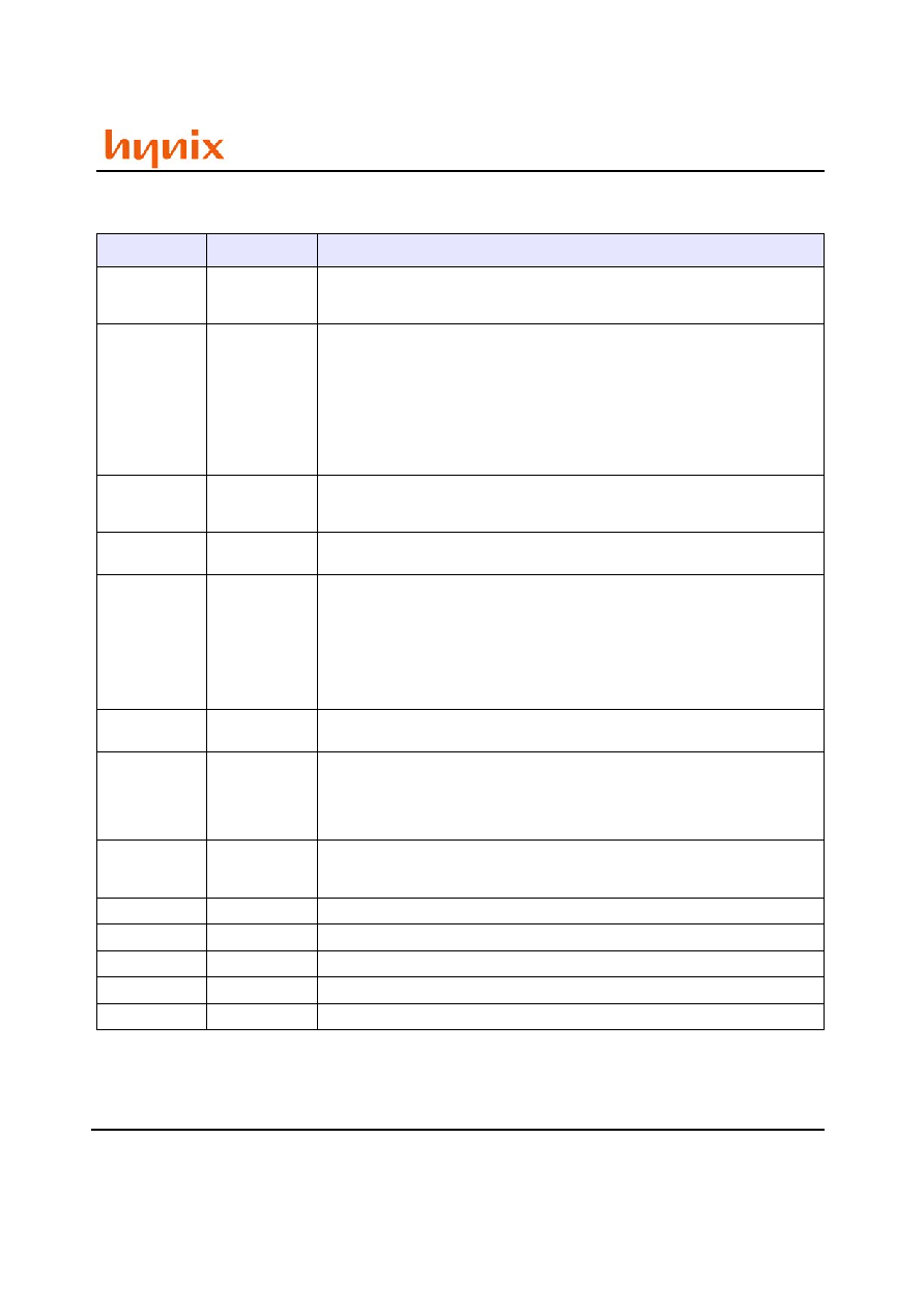
PIN DESCRIPTION
PIN
TYPE
DESCRIPTION
CK, /CK
Input
Clock: CK and /CK are differential clock inputs. All address and control input signals are
sampled on the crossing of the positive edge of CK and negative edge of /CK. Output
(read) data is referenced to the crossings of CK and /CK (both directions of crossing).
CKE
Input
Clock Enable: CKE HIGH activates, and CKE LOW deactivates internal clock signals, and
device input buffers and output drivers. Taking CKE LOW provides PRECHARGE POWER
DOWN and SELF REFRESH operation (all banks idle), or ACTIVE POWER DOWN (row
ACTIVE in any bank). CKE is synchronous for POWER DOWN entry and exit, and for SELF
REFRESH entry. CKE is asynchronous for SELF REFRESH exit, and for output disable. CKE
must be maintained high throughout READ and WRITE accesses. Input buffers, excluding
CK, /CK and CKE are disabled during POWER DOWN. Input buffers, excluding CKE are
disabled during SELF REFRESH. CKE is an SSTL_2 input, but will detect an LVCMOS LOW
level after Vdd is applied.
/CS
Input
Chip Select : Enables or disables all inputs except CK, /CK, CKE, DQS and DM. All com-
mands are masked when CS is registered high. CS provides for external bank selection on
systems with multiple banks. CS is considered part of the command code.
BA0, BA1
Input
Bank Address Inputs: BA0 and BA1 define to which bank an ACTIVE, Read, Write or PRE-
CHARGE command is being applied.
A0 ~ A11
Input
Address Inputs: Provide the row address for ACTIVE commands, and the column address
and AUTO PRECHARGE bit for READ/WRITE commands, to select one location out of the
memory array in the respective bank. A10 is sampled during a precharge command to
determine whether the PRECHARGE applies to one bank (A10 LOW) or all banks (A10
HIGH). If only one bank is to be precharged, the bank is selected by BA0, BA1. The
address inputs also provide the op code during a MODE REGISTER SET command. BA0
and BA1 define which mode register is loaded during the MODE REGISTER SET command
(MRS or EMRS).
/RAS, /CAS, /WE
Input
Command Inputs: /RAS, /CAS and /WE (along with /CS) define the command being
entered.
LDM, UDM
Input
Input Data Mask: DM(LDM,UDM) is an input mask signal for write data. Input data is
masked when DM is sampled HIGH along with that input data during a WRITE access.
DM is sampled on both edges of DQS. Although DM pins are input only, the DM loading
matches the DQ and DQS loading. LDM corresponds to the data on DQ0-Q7; UDM corre-
sponds to the data on DQ8-Q15.
LDQS, UDQS
I/O
Data Strobe: Output with read data, input with write data. Edge aligned with read data,
centered in write data. Used to capture write data. LDQS corresponds to the data on
DQ0-Q7; UDQS corresponds to the data on DQ8-Q15.
DQ0 ~ DQ15
I/O
Data input / output pin : Data Bus
V
DD
/V
SS
Supply
Power supply for internal circuits and input buffers.
V
DDQ
/V
SSQ
Supply
Power supply for output buffers for noise immunity.
V
REF
Supply
Reference voltage for inputs for SSTL interface.
NC
NC
No connection.