
HY5DU283222AQ
128M(4Mx32) DDR SDRAM
HY5DU283222AQ
Revision 0.1
April 2003
Rev. 0.1 / Apr. 2003
This document is a general product description and is subject to change without notice.

Rev. 0.1 / Apr. 2003
2
HY5DU283222AQ
128Mb (4Mx32) Double Data Rate SDRAM
Revision History
1. Revision 0.1 (Apr. 2003)
1) Preliminary

Rev. 0.1 / Apr. 2003
3
HY5DU283222AQ
128Mb (4Mx32) Double Data Rate SDRAM
CONTENTS
1. 4Mx32 DDR SDRAM Brief Information -------------------------------------------------------------------
4
1.1 Description
1.2 Feature
1.3 Ordering Information
2. Pin & PKG Information ---------------------------------------------------------------------------------------
5
2.1 Pin Configuration
2.2 Pin Description
2.3 PKG Physical Dimension
3. Functional Block Diagram -----------------------------------------------------------------------------------
8
4. Command Truth Table ----------------------------------------------------------------------------------------
9
4.1 Simplified Command Truth Table
4.2 Write Mask Truth Table
4.3 Operation Command Truth Table
4.4 CKE Function Truth Table
5. Function Description ----------------------------------------------------------------------------------------
16
5.1 Simplified State Diagram
5.2 Power up sequence and Device Initialization
5.3 MRS/EMRS definition
5.4 Device Operation
6. Absolute Maximum Rating --------------------------------------------------------------------------------
34
7. DC Operating Condition -------------------------------------------------------------------------------------
34
8. DC Characteristics --------------------------------------------------------------------------------------------
35
9. AC Operating Test Condition ------------------------------------------------------------------------------
36
10. AC Characteristics ------------------------------------------------------------------------------------------
37
11. Input /Output Capacitance & Output Load Circuit ----------------------------------------------
39
12. Timing Diagram ---------------------------------------------------------------------------------------------
40
DESCRIPTION
The Hynix HY5DU283222 is a 134,217,728-bit CMOS Double Data Rate(DDR) Synchronous DRAM, ideally suited for
the point-to-point applications which requires high bandwidth.
The Hynix 4Mx32 DDR SDRAMs offer fully synchronous operations referenced to both rising and falling edges of the
clock. While all addresses and control inputs are latched on the rising edges of the CK (falling edges of the /CK), Data,
Data strobes and Write data masks inputs are sampled on both rising and falling edges of it. The data paths are inter-
nally pipelined and 2-bit prefetched to achieve very high bandwidth. All input and output voltage levels are compatible
with SSTL_2.
FEATURES
�
V
DD
, V
DDQ
= 2.5V
� 5%
�
All inputs and outputs are compatible with SSTL_2
interface
�
JEDEC standard 20mm x 14mm 100pin LQFP with
0.65mm pin pitch
�
Fully differential clock inputs (CK, /CK) operation
�
Double data rate interface
�
Source synchronous - data transaction aligned to
bidirectional data strobe (DQS)
�
Data outputs on DQS edges when read (edged DQ)
Data inputs on DQS centers when write (centered
DQ)
�
Data(DQ) and Write masks(DM) latched on the both
rising and falling edges of the data strobe
�
All addresses and control inputs except Data, Data
strobes and Data masks latched on the rising edges
of the clock
�
Write mask byte controls by DM (DM0 ~ DM3)
�
Programmable CAS Latency 3 and 4 supported
�
Programmable Burst Length 2 / 4 / 8 with both
sequential and interleave mode
�
Internal 4 bank operations with single pulsed RAS
�
tRAS Lock-Out function supported
�
Auto refresh and self refresh supported
�
4096 refresh cycles / 32ms
�
Half strength and Matched Impedance driver option
controlled by EMRS
ORDERING INFORMATION
Part No.
Power Supply
Clock
Frequency
Max Data Rate
interface
Package
HY5DU283222AQ-33
V
DD/
V
DDQ
= 2.5V
300MHz
600Mbps/pin
SSTL_2
20mm x 14mm
100pin LQFP
HY5DU283222AQ-36
275MHz
550Mbps/pin
HY5DU283222AQ-4
250MHz
500Mbps/pin
HY5DU283222AQ-5
200MHz
400Mbps/pin
HY5DU283222AQ
128Mb (4Mx32) Double Data Rate SDRAM
PRELIMINARY
Rev. 0.1 / Apr. 2003 4
Rev. 0.1 / Apr. 2003
5
HY5DU283222AQ
128Mb (4Mx32) Double Data Rate SDRAM
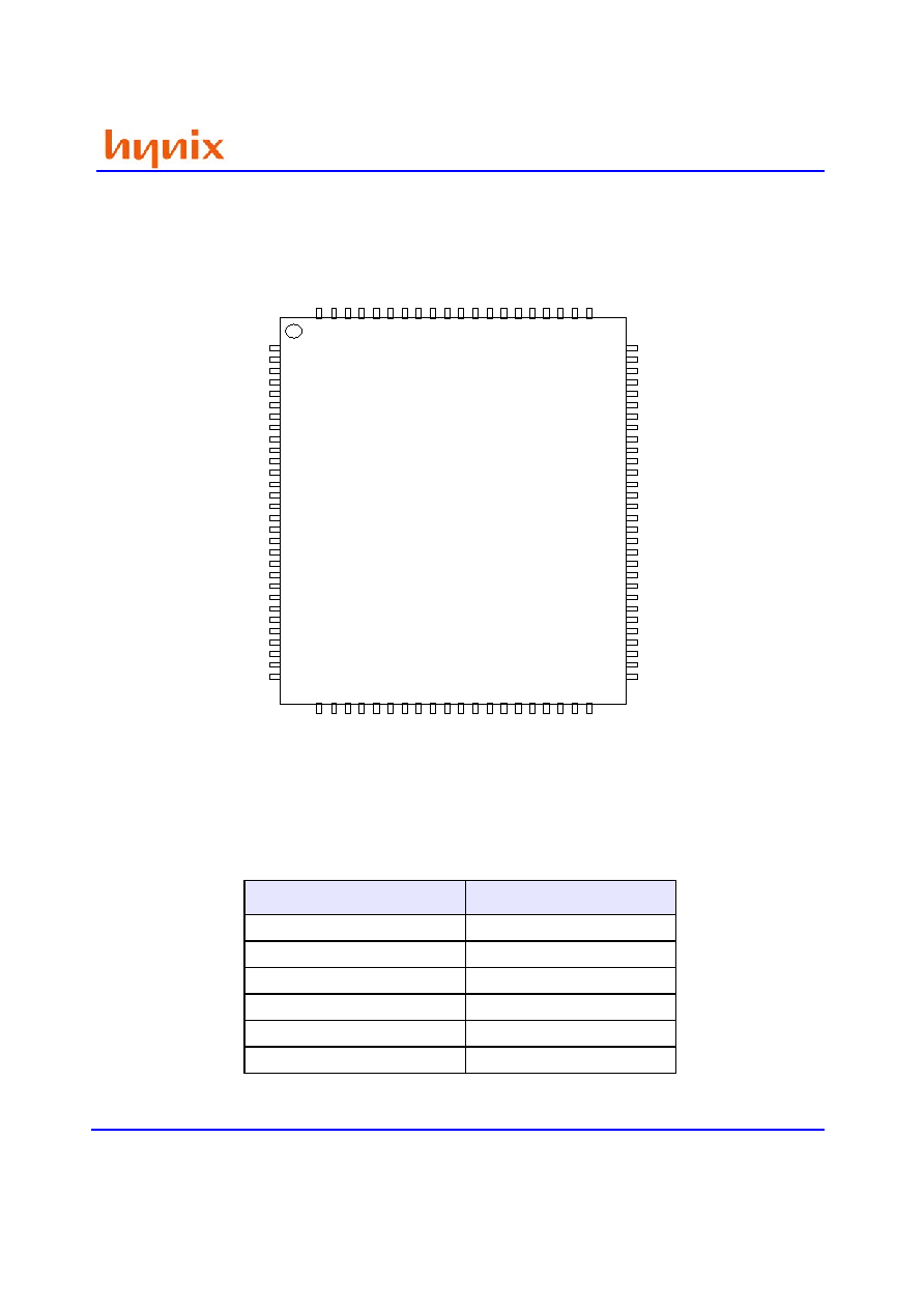
PIN CONFIGURATION
ROW and COLUMN ADDRESS TABLE
Items
4Mx32
Organization
1M x 32 x 4banks
Row Address
A0 ~ A11
Column Address
A0 ~ A7
Bank Address
BA0, BA1
Auto Precharge Flag
A8
Refresh
4K
20mm x 14mm
100Pin QFP
0.65mm Pitch
DQ3
VDDQ
DQ4
DQ5
VSSQ
DQ6
DQ7
VDDQ
DQ16
DQ17
VSSQ
DQ18
DQ19
VDDQ
VDD
VSS
DQ20
DQ21
VSSQ
DQ22
DQ23
VDDQ
DM0
DM2
/WE
/CAS
/RAS
/CS
BA0
BA1
31
32
33
34
35
36
37
38
39
40
41
42
43
44
45
46
47
48
49
50
A0
A1
A2
A3
VDD
A10
A11
NC
NC
NC
NC
NC
NC
NC
A9
VS
S
A4
A5
A6
A7
1
2
3
4
5
6
7
8
9
10
11
12
13
14
15
16
17
18
19
20
21
22
23
24
25
26
27
28
29
30
DQ28
VDDQ
DQ27
DQ26
VSSQ
DQ25
DQ24
VDDQ
DQ15
DQ14
VSSQ
DQ13
DQ12
VDDQ
VSS
VDD
DQ11
DQ10
VSSQ
DQ9
DQ8
VDDQ
VREF
DM3
DM1
CLK
/CLK
CKE
DSF, MCL
A8/AP
80
79
78
77
76
75
74
73
72
71
70
69
68
67
66
65
64
63
62
61
60
59
58
57
56
55
54
53
52
51
100
99
98
97
96
95
94
93
92
91
90
89
88
87
86
85
84
83
82
81
DQ2
VSS
Q
DQ
1
DQ
0
VDD
VDDQ
DQS
NC
VSS
Q
NC
NC
NC
NC
NC
VDDQ
VSS
DQ
3
1
DQ
3
0
V
SSQ
DQ
2
9
TOP VIEW